EP4495998A2 - Auf vorrichtungen mit breiter bandlücke (wbg) basierende dreistufige aktivneutralpunktgeklemmte (anpc) leistungsmodulentwürfe - Google Patents
Auf vorrichtungen mit breiter bandlücke (wbg) basierende dreistufige aktivneutralpunktgeklemmte (anpc) leistungsmodulentwürfe Download PDFInfo
- Publication number
- EP4495998A2 EP4495998A2 EP24185225.0A EP24185225A EP4495998A2 EP 4495998 A2 EP4495998 A2 EP 4495998A2 EP 24185225 A EP24185225 A EP 24185225A EP 4495998 A2 EP4495998 A2 EP 4495998A2
- Authority
- EP
- European Patent Office
- Prior art keywords
- power module
- semiconductor switch
- gate driving
- gate
- dies
- Prior art date
- Legal status (The legal status is an assumption and is not a legal conclusion. Google has not performed a legal analysis and makes no representation as to the accuracy of the status listed.)
- Pending
Links
Images

















Classifications
-
- H—ELECTRICITY
- H10—SEMICONDUCTOR DEVICES; ELECTRIC SOLID-STATE DEVICES NOT OTHERWISE PROVIDED FOR
- H10W—GENERIC PACKAGES, INTERCONNECTIONS, CONNECTORS OR OTHER CONSTRUCTIONAL DETAILS OF DEVICES COVERED BY CLASS H10
- H10W90/00—Package configurations
-
- H—ELECTRICITY
- H02—GENERATION; CONVERSION OR DISTRIBUTION OF ELECTRIC POWER
- H02M—APPARATUS FOR CONVERSION BETWEEN AC AND AC, BETWEEN AC AND DC, OR BETWEEN DC AND DC, AND FOR USE WITH MAINS OR SIMILAR POWER SUPPLY SYSTEMS; CONVERSION OF DC OR AC INPUT POWER INTO SURGE OUTPUT POWER; CONTROL OR REGULATION THEREOF
- H02M7/00—Conversion of AC power input into DC power output; Conversion of DC power input into AC power output
- H02M7/003—Constructional details, e.g. physical layout, assembly, wiring or busbar connections
-
- H—ELECTRICITY
- H02—GENERATION; CONVERSION OR DISTRIBUTION OF ELECTRIC POWER
- H02M—APPARATUS FOR CONVERSION BETWEEN AC AND AC, BETWEEN AC AND DC, OR BETWEEN DC AND DC, AND FOR USE WITH MAINS OR SIMILAR POWER SUPPLY SYSTEMS; CONVERSION OF DC OR AC INPUT POWER INTO SURGE OUTPUT POWER; CONTROL OR REGULATION THEREOF
- H02M7/00—Conversion of AC power input into DC power output; Conversion of DC power input into AC power output
- H02M7/42—Conversion of DC power input into AC power output without possibility of reversal
- H02M7/44—Conversion of DC power input into AC power output without possibility of reversal by static converters
- H02M7/48—Conversion of DC power input into AC power output without possibility of reversal by static converters using discharge tubes with control electrode or semiconductor devices with control electrode
- H02M7/483—Converters with outputs that each can have more than two voltages levels
- H02M7/487—Neutral point clamped inverters
Definitions
- Embodiments relate generally to power modules, and, more specifically, to WBG power modules/devices.
- Electric power components including but not limited to integrated circuits for power applications in connection with electric vehicle (EV) systems or non-vehicle systems, are susceptible to generate excessive heat and high temperature during operation.
- EV electric vehicle
- existing power modules may be based on traditional silicon devices and suffer from high power loop inductance and high gate loop inductance.
- Existing structures and layouts may not be suitable or optimal for WBG based power modules/devices such as those used in electric vehicle propulsion operations.
- the power ratings of traction motors are increasing from tens of kW to hundreds of kW and the voltages of battery packs are also increasing from 400V to 800V, which call for EV traction inverters with a rated power of 100kW or higher at a DC bus voltage of 800V. Meanwhile, the targeted power density of the EV traction inverter listed by U.S.
- DRIVE Driving Research and Innovation for Vehicle efficiency and Energy sustainability
- GaN HEMT high-electron-mobility twransistor
- DRIVE Driving Research and Innovation for Vehicle efficiency and Energy sustainability
- GaN HEMT high-electron-mobility twransistor
- fast switching speed and low switching loss that can result in smaller heatsinks and footprints, and smaller passives by switching at higher switching frequency.
- high-current GaN devices are rated at -650V, making them unfit to undertake 800Vdc directly using a two-level (2L) topology.
- 2L two-level
- power modules can be implemented with a three-level (3L) topology instead.
- a power module comprises: an upper arm structure that includes a first semiconductor switch, a second semiconductor switch and a first diode; a lower arm structure that includes a third semiconductor switch, a fourth semiconductor switch and a second diode; a first gate driving board, attached with the upper arm, wherein the first gate driving board includes a first gate driver connected to a first gate of the first semiconductor switch and a second gate driver connected to a second gate of the second semiconductor switch; a second gate driving board, attached with the lower arm, wherein the second gate driving board includes a third gate driver connected to a third gate of the third semiconductor switch and a fourth gate driver connected to a fourth gate of the fourth semiconductor switch.
- a power module comprises: an upper arm structure that includes a first semiconductor switch, a second semiconductor switch and a fifth semiconductor switch; a lower arm structure that includes a third semiconductor switch, a fourth semiconductor switch and a sixth semiconductor switch; a first gate driving board, attached with the upper arm, wherein the first gate driving board includes a first gate driver connected to a first gate of the first semiconductor switch, a second gate driver connected to a second gate of the second semiconductor switch, and a third gate driver connected to a fifth gate of the fifth semiconductor switch; a second gate driving board, attached with the lower arm, wherein the second gate driving board includes a third gate driver connected to a third gate of the third semiconductor switch, a fourth gate driver connected to a fourth gate of the fourth semiconductor switch, and a sixth gate driver connected to a sixth gate of the sixth semiconductor switch.
- Embodiments are directed to relatively low power-loop inductance, relatively low gate-drive-loop inductance, relatively low semiconductor junction-to-coolant thermal resistance and relatively low-profile power modules/devices, as compared with existing power modules/devices.
- a power module as described herein may implement a three-level neutral point clamped (3L NPC) topology or design with ultra-fast wide-band-gap (WBG) semiconductor such as gallium nitride (GaN) (e.g., vertical GaN, lateral GaN, etc.).
- 3L NPC three-level neutral point clamped
- WBG wide-band-gap
- GaN gallium nitride
- Example advantages and/or benefits provided by some or all the embodiments as described herein include, but are not necessarily limited to only: relatively low power loop inductance; integrated gate driving circuits (controlling the operations and/or operational states of semiconductor switches such as GaN-based switches); relatively low gate loop inductance; symmetrical layout with scalable (e.g., with a total number of semiconductor switches such as GaN-based switches, etc.) design; distributed terminals for balanced current sharing among (e.g., spatially, etc.) paralleled dies (containing/including semiconductor switches); decoupling capacitors on the power terminals; double-sided cooling; mechanically robust; support for Flex PCB (as well as non-Flex PCB) interconnection of gate driving circuits and/or semiconductor switches.
- An example module/device assembly process flow for assembling an NPC power module may include, but is not necessarily limited to only, any, some or all of the following steps.
- the module/device assembly process flow may include Step 1, in which (two) daughter substrates and semiconductor switches/diodes therewith are sintered to (two) mother substrates, respectively, as shown in FIG. 1A and FIG. 1B .
- the semiconductor switches/diodes may then be electrically interconnected through wire bonding.
- GaN devices or switches used herein may be of a lateral type with active regions such as gate, drain and source being all at one side. Under techniques as described herein, these GaN devices or switches can be assembled or packaged with vertical arrangement of peripheral circuits such as bus bars. Wire bonds may be used to bond all these active regions to the DBC first.
- the DBC can be connected to other bus bars in any manners convenient for the assembly. As illustrated in FIG.
- a switch gate as described herein may be at the same side of source, for example both facing upwards. Wires may be bonded directly from the gate and source to the gate driver boards. Additionally, optionally or alternatively, some or all techniques as described herein can be implemented with other switch types such as vertical devices/switches, SiC/Si devices/switches, which may have both gate and source facing up.
- FIG. 1A depicts a first mother substrate to which one or more first daughter substrates - mounted or disposed with first dies for Q2a, Q2b, D5a, D5b, Q1a and Q1b - are sintered.
- FIG. 1B depicts a second mother substrate to which one or more second daughter substrates - mounted or disposed with second dies for Q3a, Q3b, D6a, D6b, Q4a and Q4b - are sintered.
- each semiconductor switch/diode as described herein may be formed by one or more separate dies electrically connected in parallel.
- the dies Q1a and Q1b may be electrically connected in parallel and form a semiconductor switch Q1.
- the dies Q2a and Q2b may be electrically connected in parallel and form a semiconductor switch Q2.
- the dies Q3a and Q3b may be electrically connected in parallel and form a semiconductor switch Q3.
- the dies Q4a and Q4b may be electrically connected in parallel and form a semiconductor switch Q4.
- the dies D5a and D5b may be electrically connected in parallel and form a diode D5.
- the dies D6a and D6b may be electrically connected in parallel and form a diode D6.
- the module/device assembly process flow for assembling an NPC power module may include Step 2, in which (two) gate drive boards are assembled or attached to the (two) mother substrates, respectively, as shown in FIG. 2A and FIG. 2B .
- the gate drive boards may include gate driver ICs for some or all of the semiconductor switches. Gate pads of some or all of the semiconductor switches may be electrically connected with the gate driver ICs on the gate drive boards.
- a first gate drive board is assembled or attached to the first mother substrate of FIG. 1A .
- the first gate drive board includes a first gate driver IC for the semiconductor switch Q2 and a second gate driver IC for the semiconductor switch Q1. Gate pads of the semiconductor switch Q2 may be electrically connected with the first gate driver IC, whereas gate pads of the semiconductor switch Q1 may be electrically connected with the second gate driver IC.
- a second gate drive board is assembled or attached to the second mother substrate of FIG. 1B .
- the second gate drive board includes a third gate driver IC for the semiconductor switch Q3 and a fourth gate driver IC for the semiconductor switch Q4. Gate pads of the semiconductor switch Q3 may be electrically connected with the third gate driver IC, whereas gate pads of the semiconductor switch Q4 may be electrically connected with the fourth gate driver IC.
- the module/device assembly process flow for assembling an NPC power module may include Step 3, in which posts such as copper or conductive posts, a (e.g., single, etc.) neutral terminal, and so are mounted, attached, or otherwise disposed with one or both of the two mother substrates.
- posts such as copper or conductive posts, a (e.g., single, etc.) neutral terminal, and so are mounted, attached, or otherwise disposed with one or both of the two mother substrates.
- posts namely, post 2 is mounted, attached or otherwise disposed with the second mother substrate of FIG. 2B
- posts 1 and 3 are mounted, attached or otherwise disposed with the first mother substrate of FIG. 2A .
- the first and second mother substrates of FIG. 1A and FIG. 2B with the posts are then assembled with foil such as copper or conductive foil, etc., to form an electrically and/or mechanically interconnected module/device.
- the second mother substrate of FIG. 2B serves as an upper arm or board along a spatial direction represented by Z
- the first substrate of FIG. 2A serves as a lower arm or board along the same spatial direction (Z).
- the spatial direction (Z) may form a three-dimensional Cartesian coordinate system with two other spatial directions represented by X and Y (perpendicular to each other and Z), respectively.
- Both the first and second mother substrates may be (e.g., exactly, substantially, etc.) of a planar shape along the X and Y spatial directions as illustrated in FIG. 1A .
- the electrically and/or mechanically interconnected module/device may be assembled by placing or moving the upper arm/board downward or toward the lower arm/board, (1) until post 1 disposed with the lower arm/board is in actual (e.g., physical, mechanical, electrical, etc.) contact with the upper arm/board and (2) until post 2 disposed with the upper arm/board is in actual (e.g., physical, mechanical, electrical, etc.) contact with the foil, post 3 disposed with the lower arm/board and any intervening physical (e.g., thermally and/or electrically conductive, thermally and/or electrically insulating, etc.) materials.
- any intervening physical e.g., thermally and/or electrically conductive, thermally and/or electrically insulating, etc.
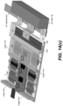
- the module/device assembly process flow for assembling an NPC power module may include Step 4, in which other parts such as other terminals (e.g., DC+, DC-, neutral point or terminal, etc.) may be assembled into the module/device from Step 3 to form the module/device of FIG. 4A ; and Step 5, in which decoupling capacitors may be assembled into the module/device from Step 4 to form the (e.g., final, functional, power switch, power inverter, to be attached with cooling plates on the upper and lower surfaces of the module, etc.) module/device of FIG. 5A .
- Step 4 in which other parts such as other terminals (e.g., DC+, DC-, neutral point or terminal, etc.) may be assembled into the module/device from Step 3 to form the module/device of FIG. 4A ; and Step 5, in which decoupling capacitors may be assembled into the module/device from Step 4 to form the (e.g., final, functional, power switch, power inverter, to be attached with
- FIG. 6A and FIG. 7A illustrate example short commutation loops and long commutation loops when the power module operates in first operational/switching states (corresponding to two first different quadrants in four quadrants) and second different operational/switching states (corresponding to two second different quadrants in four quadrants), respectively.
- Each of these commutation loops represents a specific DC electric current flow through a number of specific components such as specific semiconductor switches/diodes in the NPC power module.
- the specific DC electric current flow in the corresponding commutation loop can be effectuated by using gate driver ICs to set gates of the semiconductor switches to specific gate states.
- FIG. 6A(a) - along with FIG. 7A (a) - illustrates two short commutation loops (e.g., sharing or being clamped to the same neural terminal, etc.) formed when the power module operates in the first operational/switching states or quadrants.
- FIG. 6A(b) - along with FIG. 7A (b) - illustrates two long commutation loops (e.g., sharing or being clamped to the same neural terminal, etc.) formed when the power module operates in the second operational/switching states or quadrants.
- Flux cancelling is one of effective methods to reduce the loop inductance. By maximizing the negative mutual inductance, the total loop inductance is minimized. As illustrated in F IG. 6A and FIG. 7A , the forward current paths and the backward current paths of both the short and long commutation loops are fully overlapped, so that the magnetic flux can be canceled to the maximum extent. Additionally, optionally or alternatively, in operational scenarios in which wire-bonding connection is replaced by copper or conductive foil connection, the distance between the two mother substrates (e.g., DBCs, etc.) and the distance between the neutral terminal and mother substrates (DBCs in the present example) can be further shortened. Consequently, the loop inductances can be further reduced.
- the two mother substrates e.g., DBCs, etc.
- DBCs neutral terminal and mother substrates
- Gate driving electric currents flowing through the gate driver ICs integrated with (e.g., gate lines of, etc.) the semiconductor switches may be relatively small as compared with power loop electric currents flowing in the power loops illustrated in FIG. 6A and FIG. 7A .
- the gate driving electric currents may generate magnetic fluxes and hence generate (e.g., relatively low, etc.) gate driving loop inductances.
- the gate driving loop inductances can be minimized by the shorting (conductive or copper) trace length(s) and/or by implementing flux cancellation by concurrent gate driving loops with opposite loop directions.
- a symmetrical layout and scalable design may be used to arrange semiconductor switches and gate driving ICs.
- two dies e.g., Q1a and Q1b, etc.
- the gate driving board on which the gate driving ICs are mounted or attached may be placed in the middle of the mother substrates in the power module.
- both the power loops and gate driving loops can be made symmetrical.
- One of the prominent benefits under techniques as described herein is balanced current sharing among the parallel dies of each of the semiconductor switches while the power module is in operation.
- the power module design as described herein is also scalable with two or more dies in parallel (or parallelized) for each semiconductor switch to increase the overall power rating or capacity of the power module.
- One or more sets of gate driving circuits or ICs can be used accordingly.
- One or more gate driving boards can also be at on one or both sides (e.g., upper and/or lower side(s) in the X-Y plane of each of the mother substrates, etc.) of the power module.
- the symmetry of the gate driving loops may be lost or may not be maintained while the symmetry of the power loop can be maintained.
- physical materials or substrate(s) (e.g., directly, etc.) underneath the gate driving board need not to be those of direct bonded copper (DBC), which may reduce or lower costs for DBC in the power module.
- DBC direct bonded copper
- FIG. 2C illustrates an example gate driving board placed on one side (in the X-Y plane) of a mother substrate of the power module
- FIG. 2D illustrates an example gate driving board placed on both sides (in the X-Y plane) of a mother substrate of the power module.
- physical materials or substrate(s) (e.g., directly, etc.) underneath each of these gate driving boards in FIG. 2C and FIG. 2D may not be those of direct bonded copper (DBC).
- DBC direct bonded copper
- Distributed terminals such as wide DC bus terminals can be used for some or all positive, negative and neutral terminals to help achieve balanced current sharing among parallel dies of each of some or all semiconductor switch in the power module. These terminals can be specifically designed or spatially structured for mounting two sets of decoupling capacitors as well as providing mechanical support for the power module.
- Decoupling capacitors are mounted on the (e.g., distributed, etc.) DC or power terminals away from the heat sources which are semiconductor devices/switches/ICs. At the same time, these capacitors can be cooled by cold plates attached with the power module to keep relatively low capacitor temperature to increase their service times. In addition, such a design facilitates replacement operations for some or all of decoupling capacitors after the power module is deployed in the field, as these capacitors may represent one of common failure points for power module operations.
- Those decoupling capacitors can be horizontally or vertically mounted on the wide power terminals. For example, as illustrated in FIG. 5A , decoupling capacitors may be horizontally mounted on the distributed terminals. Also as illustrated in FIG. 5B , decoupling capacitors may be vertically mounted on the distributed terminals.
- Cooling plates may be used to keep the power module at a relatively low operational temperature.
- Some or all of the semiconductor devices/switches/ICs in the power module can be mounted on or in physical/thermal contact with one or both of two mother substrates such as direct bonded copper (DBC) substrates.
- two mother substrates such as direct bonded copper (DBC) substrates.
- DBC direct bonded copper
- one or both of those mother substrates can be in (e.g., direct, etc.) thermal or physical contact with one or more cooling plates to extract or dissipate heat generated by semiconductor switches/diodes and/or by other components of the power module in operation.
- FIG. 8A illustrates two example cooling plates used to sandwich the mother substrates of the power module in between.
- the power module is double-sided cooled, which can be used to support or achieve high-power density and compact design for the power module.
- Top and bottom substrates in the power module/device includes conductive (e.g., rigid, etc.) copper blocks/posts, which function as both as part of electrical paths in operation as well as mechanical support.
- conductive e.g., rigid, etc.
- FIG. 9A there are three mechanical or copper supports in the power module/device.
- the first copper support is located in the front end (DC link side) of the power module/device.
- the second copper support is located in the middle of the power module/device.
- the third support is located in the back end (AC output side) of the power module/device.
- the DC+, DC- and N (neutral) terminals can be laminated copper bars with a thin layer of insulation material, such as Kapton tapes inserted between any two of those terminal bus bars. Additionally, optionally or alternatively, areas underneath the decoupling capacitors can be solid (materials) to provide mechanical or structural support. Hence, mechanical pressure from the cold plates sandwiching (the upper and lower mother substrates of) the power module/device can be well balanced as compared with other approaches that do not implement techniques as described herein.
- pads of some or all of the semiconductor switches in the power module/device can be connected through bond wires. Additionally, optionally or alternatively, the semiconductor switches or their pads can be interconnected through other electrically and/or thermally conductive metal plates to shrink the clearance or spacing of substrates.
- the gate driving circuit or IC components can be mounted on a rigid PCB.
- the gate driving circuits can be connected with gate pads of the semiconductor devices by bond wires.
- the PCB can be rigid/flex PCB with the components on the rigid part; the semiconductor switches and gate driving circuits can be connected by the flex part.
- a power module comprises: an upper arm structure that includes a first semiconductor switch, a second semiconductor switch and a first diode; a lower arm structure that includes a third semiconductor switch, a fourth semiconductor switch and a second diode; a first gate driving board, attached with the upper arm, the first gate driving board including a first gate driver connected to a first gate of the first semiconductor switch and a second gate driver connected to a second gate of the second semiconductor switch; a second gate driving board, attached with the lower arm, the second gate driving board including a third gate driver connected to a third gate of the third semiconductor switch and a fourth gate driver connected to a fourth gate of the fourth semiconductor switch.
- first electric currents of equal magnitudes flow in two short commutation loops when the power module operates in first operational states.
- second electric currents of equal magnitudes flow in two long commutation loops when the power module operates in second operational states.
- the upper arm structure includes a first mother substrate to which the first diode is directly attached; the lower arm structure includes a second mother substrate to which the second diode is directly attached.
- the first semiconductor switch, the second semiconductor switch and the first diode on the upper arm structure form a spatial symmetry with the third semiconductor switch, the fourth semiconductor switch and the second diode on the lower arm structure.
- the power module further comprises: a direct current (DC) positive terminal (DC+); a DC negative terminal (DC-).
- DC direct current
- DC+ direct current positive terminal
- DC- DC negative terminal
- spatial planes of the lower and upper arm structures are parallel to each other; the DC+ and DC- are vertically arranged relative to the spatial planes of the lower and upper arm structures.
- spatial planes of the lower and upper arm structures are parallel to each other; the DC+ and DC- are horizontally arranged relative to the spatial planes of the lower and upper arm structures.
- the first, second, third and fourth semiconductor switches include a first vertical Gallium Nitrate (GaN) switch disposed on the upper arm structure and a second vertical GaN switch disposed on the lower arm structure; the first and second vertical GaN switches form a spatial symmetry to each other.
- GaN vertical Gallium Nitrate
- the first, second, third and fourth semiconductor switches include a first lateral Gallium Nitrate (GaN) switch disposed on the upper arm structure and a second lateral GaN switch disposed on the lower arm structure; the first and second lateral GaN switches form a spatial symmetry to each other.
- GaN Gallium Nitrate
- each of the first, second, third and fourth semiconductor switches includes two semiconductor switch dies.
- the first and second gate driving boards include a gate driving board that is centrally located in between the two semiconductor switch dies; the gate driving board includes a first gate driving circuit connected to a first die of the two semiconductor switch dies and a second gate driving circuit connected to a second die of the two semiconductor switch dies.
- the first and second gate driving boards include a gate driving board that is centrally located on a same side of the two semiconductor switch dies; wherein the gate driving board includes a first gate driving circuit connected to a first die of the two semiconductor switch dies and a second gate driving circuit connected to a second die of the two semiconductor switch dies.
- the first and second gate driving boards include a gate driving board having a first gate driving board portion located at a first side of the two semiconductor switch dies and a second gate driving board portion located at a second different side of the two semiconductor switch dies; the first gate driving board portion includes a first gate driving circuit connected to a first die of the two semiconductor switch dies; the second gate driving board portion includes a second gate driving circuit connected to a second die of the two semiconductor switch dies.
- the power module further comprises: an alternate current (AC) terminal.
- AC alternate current
- the AC terminal is located on a first side plane formed between the upper and lower art structures; a direct current (DC) positive terminal (DC+), a DC negative terminal (DC-), and a neutral terminal (N) of the power module are located on a second opposing plane formed between the upper and lower art structures.
- DC direct current
- DC+ DC positive terminal
- DC- DC negative terminal
- N neutral terminal
- the DC+ and the N are electrically connected with a first group of decoupling capacitors; the DC- and the N are electrically connected with a second group of decoupling capacitors.
- the power module further comprises: two or more posts mechanically attached to the upper and lower arm structures.
- the upper arm structure is attached to a first cooling plate on a first side of the power module; the lower arm structure is attached to a second different cooling plate on a second opposing side of the power module.
- one or more of the first, second, third and fourth semiconductor switches and the first and second diodes are attached to one or more of two mother substrates of the upper and lower arm structures by way of one or more daughter substrates.
- three level ANPC (3L ANPC) topology with WBG devices may be implemented by directly mounting semiconductor devices on a printed circuit board (PCB).
- PCB printed circuit board
- One benefit from these ANPC devices may be to better balance power loss distributions over time in realtime field operations as compared with the NPC devices.
- the thermal performance of such an approach and the electric current carrying capability of PCBs are relatively low. Hence, a supported power level of such an approach may be limited to relatively low power applications.
- Embodiments are directed to relatively low power-loop inductance, relatively low gate-drive-loop inductance, relatively low semiconductor junction-to-coolant thermal resistance and relatively low-profile power modules/devices, as compared with existing power modules/devices.
- a power module as described herein may implement a three-level active neutral point clamped (ANPC) topology or design with ultra-fast WBG semiconductor such as gallium nitride (GaN).
- ANPC active neutral point clamped
- GaN gallium nitride
- Example advantages and/or benefits provided by some or all the embodiments as described herein include, but are not necessarily limited to only: relatively low power loop inductance; integrated gate driving circuits (with semiconductor switches such as GaN-based switches); relatively low gate loop inductance; symmetrical layout with scalable (e.g., with a total number of semiconductor switches such as GaN-based switches, etc.) design; distributed terminals for balanced current sharing among (e.g., spatially, etc.) paralleled dies (containing/including semiconductor switches); decoupling capacitors on the power terminals; double-sided cooling; mechanically robust; stacking substrates design; support for Flex PCB (as well as non-Flex PCB) interconnection of gate driving circuits and/or semiconductor switches.
- An example module/device assembly process flow for assembling an ANPC power module may include, but is not necessarily limited to only, any, some or all of the following steps.
- the module/device assembly process flow may include Step 1, in which (two) daughter substrates and dies for semiconductor switches therewith are sintered to (two) mother substrates, respectively, as shown in FIG. 1C and FIG. 1D .
- the semiconductor switches or dies containing the semiconductor switches may then be electrically interconnected through wire bonding.
- GaN devices or switches used herein may be of a lateral type with active regions such as gate, drain and source being all at one side. Under techniques as described herein, these GaN devices or switches can be assembled or packaged with vertical arrangement of peripheral circuits such as bus bars. Wire bonds may be used to bond all these active regions to the DBC first.
- the DBC can be connected to other bus bars in any manners convenient for the assembly. As illustrated in FIG.
- a switch gate as described herein may be at the same side of source, for example both facing upwards. Wires may be bonded directly from the gate and source to the gate driver boards. Additionally, optionally or alternatively, some or all techniques as described herein can be implemented with other switch types such as vertical devices/switches, SiC/Si devices/switches, which may have both gate and source facing up.
- FIG. 1C depicts a first mother substrate to which one or more first daughter substrates - mounted or disposed with first dies Q2a and Q2b, Q5a, Q5b, Q1a and Q1b - are sintered.
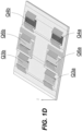
- FIG. 1D depicts a second mother substrate to which one or more second daughter substrates - mounted or disposed with second dies for Q3a, Q3b, Q6a, Q6b, Q4a and Q4b - are sintered.
- each semiconductor switch as described herein may be formed by one or more separate dies electrically connected in parallel.
- the dies Q1a and Q1b may be electrically connected in parallel and form a semiconductor switch Q1.
- the dies Q2a and Q2b may be electrically connected in parallel and form a second semiconductor switch Q2.
- the dies Q3a and Q3b may be electrically connected in parallel and form a semiconductor switch Q3.
- the dies Q4a and Q4b may be electrically connected in parallel and form a second semiconductor switch Q4.
- the dies Q5a and Q5b may be electrically connected in parallel and form a semiconductor switch Q5.
- the dies Q6a and Q6b may be electrically connected in parallel and form a semiconductor switch Q6.
- the module/device assembly process flow for assembling an ANPC power module may include Step 2, in which (two) gate drive boards are assembled or attached to the (two) mother substrates, respectively, as shown in FIG. 2E and FIG. 2F .
- the gate drive boards may include gate driver ICs for some or all of the semiconductor switches. Gate pads of some or all of the semiconductor switches may be electrically connected with the gate driver ICs on the gate drive boards.
- a first gate drive board is assembled or attached to the first mother substrate of FIG. 1C .
- the first gate drive board includes a first gate driver IC for the semiconductor switch Q2, a second gate driver IC for the semiconductor switch Q1, and a fifth gate driver IC for the semiconductor switch Q5.
- Gate pads of the semiconductor switch Q2 may be electrically connected with the first gate driver IC.
- Gate pads of the semiconductor switch Q1 may be electrically connected with the second gate driver IC.
- Gate pads of the semiconductor switch Q5 may be electrically connected with the fifth gate driver IC.
- a second gate drive board is assembled or attached to the second mother substrate of FIG. 1D .
- the second gate drive board includes a third gate driver IC for the semiconductor switch Q3, a fourth gate driver IC for the semiconductor switch Q4, and a sixth gate driver IC for the semiconductor switch Q6.
- Gate pads of the semiconductor switch Q3 may be electrically connected with the third gate driver IC.
- Gate pads of the semiconductor switch Q4 may be electrically connected with the fourth gate driver IC.
- Gate pads of the semiconductor switch Q6 may be electrically connected with the sixth gate driver IC.
- the module/device assembly process flow for assembling an ANPC power module may include Step 3, in which posts such as copper posts conductive posts, a (e.g., single, etc.) neutral terminal, and so are mounted, attached, or otherwise disposed with one or both of the two mother substrates.
- posts such as copper posts conductive posts, a (e.g., single, etc.) neutral terminal, and so are mounted, attached, or otherwise disposed with one or both of the two mother substrates.
- posts namely, post 2 is mounted, attached or otherwise disposed with the second mother substrate of FIG. 2F
- posts 1 and 3 are mounted, attached or otherwise disposed with the first mother substrate of FIG. 2E .
- the first and second mother substrates of FIG. 2E and FIG. 2F with the posts are then assembled with foil such as copper or conductive foil, etc., to form an electrically and/or mechanically interconnected module/device.
- the second mother substrate of FIG. 2F serves as an upper arm or board along a spatial direction represented by Z
- the first substrate of FIG. 2E serves as a lower arm or board along the same spatial direction (Z).
- the spatial direction (Z) may form a three-dimensional Cartesian coordinate system with two other spatial directions represented by X and Y (perpendicular to each other and Z), respectively.
- Both the first and second mother substrates may be (e.g., exactly, substantially, etc.) of a planar shape along the X and Y spatial directions as illustrated in FIG. 1C .
- the electrically and/or mechanically interconnected module/device may be assembled by placing or moving the upper arm/board downward or toward the lower arm/board, (1) until post 1 disposed with the lower arm/board is in actual (e.g., physical, mechanical, electrical, etc.) contact with the upper arm/board and (2) until post 2 disposed with the upper arm/board is in actual (e.g., physical, mechanical, electrical, etc.) contact with the foil, post 3 disposed with the lower arm/board and any intervening physical (e.g., thermally and/or electrically conductive, thermally and/or electrically insulating, etc.) materials.
- any intervening physical e.g., thermally and/or electrically conductive, thermally and/or electrically insulating, etc.
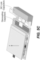
- the module/device assembly process flow for assembling an ANPC power module may include Step 4, in which other parts such as other terminals (e.g., DC+, DC-, neutral point or terminal, etc.) may be assembled into the module/device from Step 3 to form the module/device of FIG. 4B ; and Step 5, in which decoupling capacitors and DC link capacitors may be assembled into the module/device from Step 4 to form the (e.g., final, functional, power switch, power inverter, to be attached with cooling plates on the upper and lower surfaces of the module, etc.) module/device of FIG. 5C .
- Step 4 in which other parts such as other terminals (e.g., DC+, DC-, neutral point or terminal, etc.) may be assembled into the module/device from Step 3 to form the module/device of FIG. 4B ; and Step 5, in which decoupling capacitors and DC link capacitors may be assembled into the module/device from Step 4 to form the (e.g., final, functional, power
- FIG. 6B and FIG. 7B illustrate example short commutation loops and long commutation loops when the power module operates in first operational/switching states (corresponding to two first different quadrants in four quadrants) and second different operational/switching states (corresponding to two second different quadrants in four quadrants), respectively.
- Each of these commutation loops represents a specific DC electric current flow through a number of specific components such as specific semiconductor switches in the ANPC power module.
- the specific DC electric current flow in the corresponding commutation loop can be effectuated by using gate driver ICs to set gates of the semiconductor switches to specific gate states.
- FIG. 6B(a) - along with FIG. 7B (a) - illustrates two short commutation loops (e.g., sharing or being clamped to the same neural terminal, etc.) formed when the power module operates in the first operational/switching states or quadrants.
- FIG. 6B(b) - along with FIG. 7B (b) - illustrates two long commutation loops (e.g., sharing or being clamped to the same neural terminal, etc.) formed when the power module operates in the second operational/switching states or quadrants.
- Flux cancelling is one of effective methods to reduce the loop inductance. By maximizing the negative mutual inductance, the total loop inductance is minimized. As illustrated in FIG. 6B and FIG. 7B , the forward current paths and the backward current paths of both the short and long commutation loops are fully overlapped, so that the magnetic flux can be canceled to the maximum extent. Additionally, optionally or alternatively, in operational scenarios in which wire-bonding connection is replaced by copper or conductive foil connection, the distance between the two mother substrates (e.g., DBCs, etc.) and the distance between the neutral terminal and mother substrates (DBCs in the present example) can be further shortened. Consequently, the loop inductances can be further reduced.
- the two mother substrates e.g., DBCs, etc.
- DBCs neutral terminal and mother substrates
- Gate driving electric currents flowing through the gate driver ICs integrated with (e.g., gate lines of, etc.) the semiconductor switches may be relatively small as compared with power loop electric currents flowing in the power loops illustrated in FIG. 6B and FIG. 7B .
- the gate driving electric currents may generate magnetic fluxes and hence generate (e.g., relatively low, etc.) gate driving loop inductances.
- the gate driving loop inductances can be minimized by the shorting (conductive or copper) trace length(s) and/or by implementing flux cancellation by concurrent gate driving loops with opposite loop directions.
- a symmetrical layout and scalable design may be used to arrange semiconductor switches and gate driving ICs.
- two dies e.g., Q1a and Q1b, etc.
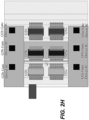
- the gate driving board on which the gate driving ICs are mounted or attached may be placed in the middle of the mother substrates in the power module.
- both the power loops and gate driving loops can be made symmetrical.
- One of the prominent benefits under techniques as described herein is balanced current sharing among the parallel dies of each of the semiconductor switches while the power module is in operation.
- the power module design as described herein is also scalable with two or more dies in parallel (or parallelized) for each semiconductor switch to increase the overall power rating or capacity of the power module.
- One or more sets of gate driving circuits or ICs can be used accordingly.
- One or more gate driving boards can also be at on one or both sides (e.g., upper and/or lower side(s) in the X-Y plane of each of the mother substrates, etc.) of the power module.
- the symmetry of the gate driving loops may be lost or may not be maintained while the symmetry of the power loop can be maintained.
- physical materials or substrate(s) (e.g., directly, etc.) underneath the gate driving board need not to be those of direct bonded copper (DBC), which may reduce or lower costs for DBC in the power module.
- DBC direct bonded copper
- FIG. 2G illustrates an example gate driving board placed on one side (in the X-Y plane) of a mother substrate of the power module
- FIG. 2H illustrates an example gate driving board placed on both sides (in the X-Y plane) of a mother substrate of the power module.
- Physical materials or substrate(s) (e.g., directly, etc.) underneath each of these gate driving boards in FIG. 2G and FIG. 2H need not to be those of direct bonded copper (DBC).
- DBC direct bonded copper
- Distributed terminals such as wide DC bus terminals can be used for some or all positive, negative and neutral terminals to help achieve balanced current sharing among parallel dies of each of some or all semiconductor switch in the power module. These terminals can be specifically designed or spatially structured for mounting two sets of decoupling capacitors as well as providing mechanical support for the power module.
- Decoupling capacitors are mounted on the (e.g., distributed, etc.) DC or power terminals away from the heat sources which are semiconductor devices/switches/ICs. At the same time, these capacitors can be cooled by cold plates attached with the power module to keep relatively low capacitor temperature to increase their service times. In addition, such a design facilitates replacement operations for some or all of decoupling capacitors after the power module is deployed in the field, as these capacitors may represent one of common failure points for power module operations.
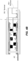
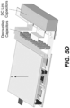
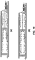
- Those decoupling capacitors can be horizontally or vertically mounted on the wide power terminals. For example, as illustrated in FIG. 5C , decoupling capacitors may be horizontally mounted on the distributed terminals. Also as illustrated in FIG. 5D , decoupling capacitors may be vertically mounted on the distributed terminals.
- Cooling plates may be used to keep the power module at a relatively low operational temperature.
- Some or all of the semiconductor devices/switches/ICs in the power module can be mounted on or in physical/thermal contact with one or both of two mother substrates such as direct bonded copper (DBC) substrates.
- two mother substrates such as direct bonded copper (DBC) substrates.
- DBC direct bonded copper
- one or both of those mother substrates can be in (e.g., direct, etc.) thermal or physical contact with one or more cooling plates to extract or dissipate heat generated by semiconductor switches and/or by other components of the power module in operation.
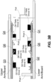
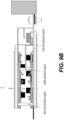
- FIG. 8B illustrates two example cooling plates used to sandwich the mother substrates of the power module in between.
- the power module is double-sided cooled, which can be used to support or achieve high-power density and compact design for the power module.
- top and bottom substrates in the power module/device includes conductive (e.g., rigid, etc.) copper blocks/posts. These blocks/posts can function as both as part of electrical paths in operation as well as mechanical support.
- conductive e.g., rigid, etc.
- FIG. 9B there are three mechanical or copper supports in the power module/device.
- the first copper support is located in the front end (DC link side) of the power module/device.
- the second copper support is located in the middle of the power module/device.
- the third support is located in the back end (AC output side) of the power module/device.
- the DC+, DC- and N (neutral) terminals can be laminated copper bars with a thin layer of insulation material, such as Kapton tapes inserted between any two of those terminal bus bars. Additionally, optionally or alternatively, areas underneath the decoupling capacitors can be solid (materials) to provide mechanical or structural support. Hence, mechanical pressure from the cold plates sandwiching (the upper and lower mother substrates of) the power module/device can be well balanced as compared with other approaches that do not implement techniques as described herein.
- pads of some or all of the semiconductor switches in the power module/device can be connected through bond wires. Additionally, optionally or alternatively, the semiconductor switches or their pads can be interconnected through other electrically and/or thermally conductive metal plates to shrink the clearance or spacing of substrates.
- the gate driving circuit or IC components can be mounted on a rigid PCB.
- the gate driving circuits can be connected with gate pads of the semiconductor devices by bond wires.
- the PCB can be a rigid/flex PCB with the components on the rigid part; the semiconductor switches and gate driving circuits can be connected by the flex part.
- One or more daughter substrates as described herein may be patched on a mother DBC substrate to provide or accommodate interconnections of semiconductor devices such as three power semiconductor switches by providing one or more additional or other conduction layers, as illustrated in FIG. 10 .
- one or more edges of the daughter substrates can be connected to the mother (e.g., DBC, etc.) substrate by conductive solder.
- the mother e.g., DBC, etc.
- conductive solder e.g., conductive solder
- isolated islands could be created on the mother substrate instead of or in addition to using patched daughter substrates.
- the symmetry of the power loops might be lost, and the size of the power module might increase, for example laterally along one or both or the spatial dimensions of the mother substrate for the purpose of accommodating additional switch(es) which could otherwise be mounted on daughter substrate(s) separate from and stacked over the mother substrate.
- a power module comprises: an upper arm structure that includes a first semiconductor switch, a second semiconductor switch and a fifth semiconductor switch; a lower arm structure that includes a third semiconductor switch, a fourth semiconductor switch and a sixth semiconductor switch; a first gate driving board, attached with the upper arm, the first gate driving board including a first gate driver connected to a first gate of the first semiconductor switch, a second gate driver connected to a second gate of the second semiconductor switch, and a third gate driver connected to a fifth gate of the fifth semiconductor switch; a second gate driving board, attached with the lower arm, the second gate driving board including a third gate driver connected to a third gate of the third semiconductor switch, a fourth gate driver connected to a fourth gate of the fourth semiconductor switch, and a sixth gate driver connected to a sixth gate of the sixth semiconductor switch.
- first electric currents of equal magnitudes flow in two short commutation loops when the power module operates in first operational states.
- second electric currents of equal magnitudes flow in two long commutation loops when the power module operates in second operational states.
- the upper arm structure includes a first mother substrate to which the fifth semiconductor switch is directly attached; the lower arm structure includes a second mother substrate to which the sixth semiconductor switch is directly attached.
- the first, second and fifth semiconductor switches on the upper arm structure form a spatial symmetry with the third, fourth and sixth semiconductor switches on the lower arm structure.
- the power module further comprises: a direct current (DC) positive terminal (DC+); a DC negative terminal (DC-).
- DC direct current
- DC+ direct current positive terminal
- DC- DC negative terminal
- spatial planes of the lower and upper arm structures are parallel to each other; the DC+ and DC- are vertically arranged relative to the spatial planes of the lower and upper arm structures.
- spatial planes of the lower and upper arm structures are parallel to each other; the DC+ and DC- are horizontally arranged relative to the spatial planes of the lower and upper arm structures.
- the first, second, third, fourth, fifth and sixth semiconductor switches include a first vertical Gallium Nitrate (GaN) switch disposed on the upper arm structure and a second vertical GaN switch disposed on the lower arm structure; the first and second vertical GaN switches form a spatial symmetry to each other.
- GaN vertical Gallium Nitrate
- the first, second, third, fourth, fifth and sixth semiconductor switches include a first lateral Gallium Nitrate (GaN) switch disposed on the upper arm structure and a second lateral GaN switch disposed on the lower arm structure; the first and second lateral GaN switches form a spatial symmetry to each other.
- GaN Gallium Nitrate
- each of the first, second, third, fourth, fifth and sixth semiconductor switches includes two semiconductor switch dies.
- the first and second gate driving boards include a gate driving board that is centrally located in between the two semiconductor switch dies; the gate driving board includes a first gate driving circuit connected to a first die of the two semiconductor switch dies and a second gate driving circuit connected to a second die of the two semiconductor switch dies.
- the first and second gate driving boards include a gate driving board that is centrally located on a same side of the two semiconductor switch dies; the gate driving board includes a first gate driving circuit connected to a first die of the two semiconductor switch dies and a second gate driving circuit connected to a second die of the two semiconductor switch dies.
- the first and second gate driving boards include a gate driving board having a first gate driving board portion located at a first side of the two semiconductor switch dies and a second gate driving board portion located at a second different side of the two semiconductor switch dies; the first gate driving board portion includes a first gate driving circuit connected to a first die of the two semiconductor switch dies; the second gate driving board portion includes a second gate driving circuit connected to a second die of the two semiconductor switch dies.
- the power module further comprises: an alternate current (AC) terminal.
- AC alternate current
- the AC terminal is located on a first side plane formed between the upper and lower art structures; a direct current (DC) positive terminal (DC+), a DC negative terminal (DC-), and a neutral terminal (N) of the power module are located on a second opposing plane formed between the upper and lower art structures.
- DC direct current
- DC+ DC positive terminal
- DC- DC negative terminal
- N neutral terminal
- the DC+ and the N are electrically connected with a first group of decoupling capacitors; the DC- and the N are electrically connected with a second group of decoupling capacitors.
- the power module further comprises: two or more posts mechanically attached to the upper and lower arm structures.
- the upper arm structure is attached to a first cooling plate on a first side of the power module; the lower arm structure is attached to a second different cooling plate on a second opposing side of the power module.
- one or more of the first, second, third, fourth, fifth and sixth semiconductor switches are attached to one or more of two mother substrates of the upper and lower arm structures by way of one or more daughter substrates.
- first As used herein, the terms “first,” “second,” “certain,” and “particular” are used as naming conventions to distinguish queries, plans, representations, steps, objects, devices, or other items from each other, so that these items may be referenced after they have been introduced. Unless otherwise specified herein, the use of these terms does not imply an ordering, timing, or any other characteristic of the referenced items.
- each component may feature a suitable communication interface by which the component may become communicatively coupled to other components as needed to accomplish any of the functions described herein.
- the simulated loop inductances are 1.92nH for the short loops and 5.21nH for the long loops, respectively; resulting in a 471V and 540V of turn-off voltage spikes in a double pulse test simulation at 400V/200A.
- the simulated junction-to-coolant thermal resistances are 0.37oC/W and 0.53 oC/W for different switches, respectively.
- the power ratings of traction motors are increasing from tens of kW to hundreds of kW and the voltages of battery packs are also increasing from 400V to 800V, which call for EV traction inverters with a rated power of 100kW or higher at a DC bus voltage of 800V [1, 2].
- the targeted power density of the EV traction inverter listed by U.S. DRIVE is increasing from 13.4 kW/L by 2020 to 33kW/L by 2025[3], making GaN HEMT a promising candidate due to its fast switching speed and low switching loss that can result in smaller heatsinks and footprints, and smaller passives by switching at higher switching frequency [4].
- GaN-based 3L-ANPC inverters advantageous in terms of efficiency, particularly in the light and medium load since 95% of an typical EV driving cycle running at less than 30% of full load [2].
- GaN HEMTs very sensitive to loop parasitic inductance [7]. Therefore, meticulous packaging design to reduce parasitic loop inductance is essential to fully exploit their benefits resulting from fast switching speed.
- the reported GaN HEMT power modules in literature are mainly focused on packaging 2L half bridge [8]. This paper, to the best knowledge of the authors, for the first time reports the packaging of 3L-ANPC phase leg power module based on 650V/150A GaN HEMT. TABLE I.
- the loads of EV traction inverter are permanent magnet (PM) motors or induction motors with a lagging power factor around 0.8-0.9, and space vector pulse width modulation (SVPWM) are adopted for the inverter modulation.
- PM permanent magnet
- SVPWM space vector pulse width modulation
- the inverter must be capable of 4-quadrant operation, yielding four commutation loops, as shown in FIG. 12 (a) and (b) , two short commutation loops and two long commutation loops [9]. Only two switches involved in the two short commutation loops. However, four switches are involved in the two long commutation loops, which unavoidably increases the loops inductance. Those loop inductances must be reduced simultaneously.
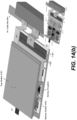
- two mother direct bonded copper substrates (DBCs) and two daughter DBCs are adopted to construct a 3L-ANPC phase leg power module, with each set of DBCs accommodating an arm of a phase leg and the neutral terminal sandwiched in the middle as shown in FIG. 14 (a) , (b) and (c) .
- the daughter DBCs are attached to the mother DBCs with one edge of the daughter DBC connected to the mother DBC.
- the switches Q1, Q2, Q3 and Q4 are attached to the two mother DBCs, while the neutral switches Q5 and Q6 are attached to the two daughter DBCs, respectively.
- the daughter DBCs only serve for die attachment and sitting the wire bonding points.
- FIG. 13 illustrates example gate signals of a 3L-ANPC phase leg (e.g., as shown in FIG. 14 (a) through (c) , etc.).
- Two long copper posts are used to connect the top mother DBC (lower arm) and bottom mother DBC (upper arm), and four short copper posts are used to connect the two neutral switches to the neutral terminal. They also provide the mechanical support and withstand the mechanical stresses from the top and bottom cold plates. Distributed terminals with a thin layer of Kapton coating are adopted. Two sets of decoupling capacitors are placed on those wide terminals. Besides connecting the power module and DC-Link capacitor, they also serve to (a) accommodate the decoupling capacitors, (b) evenly distribute the current among the two parallel dies in steady state (fundamental frequency) and during fast transient commutation period as shown in FIG. 15 , (c) cool the decoupling capacitors, and (d) provide mechanical support on the DC-Link side.
- the two short commutation loops and two long commutation loops are marked in FIG. 16 (a) and (b) , respectively.
- Flux cancelling is one of effective methods to reduce the loop inductance [10].
- the total loop inductance is minimized.
- the forward current paths and the backward current paths of both the short and long commutation loops are fully overlapped, so that the magnetic flux can be canceled to the maximum extent.
- the loop inductances are still very low: 1.92nH and 5.21nH at 100MHz for the short commutation loops and long commutation loops, respectively.
- Double pulse test (DPT) simulation is then carried out by LTSpice.
- the maximum Vds is 540V for the long commutation loops and 471V for the short commutation loops at a 400V DC bus voltage and 200A switch current, representing 135% and 118% of the DC bus voltage, respectively. This maximum voltage is in the safe operating region of the 650V devices.
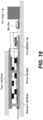
- the power module is sandwiched between two cold plates and double-sided cooled as illustrated in FIG. 18 .
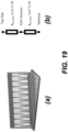
- the thermal network model of the used GaN die is given in FIG. 19 (a) and (b) , in which the junction-to-substrate thermal resistance and junction-to-top side thermal resistance are 0.07oC/W and 0.18oC/W. Due to the small contact area between the bond wires and the die, little heat are conducted to the DBC by the bond wires. The heat is mainly dissipated through the substrate side.
- the junction-to-coolant thermal network model of Q1 ⁇ Q4 and Q5 ⁇ Q6 are given in FIG. 20 (a) and (b) , respectively.
- R th,J2Sub , R th,DA , R th,M-DBC , R th,D-DBC , R th,Sd , R th,CP are thermal resistance of GaN die junction-to-substrate, die attachment layer, mother DBC, daughter DBC, solder layer and cold plate, respectively.
- the die attachment layer even very thin, can contribute significant portion of the total thermal resistance [11].
- the temperature map simulated by ANSYS Icepak with 35W per die, copper cold plate thickness 5mm and constant coolant temperature at 85oC is shown in FIG. 21 .
- the maximum junction temperatures of Q1 ⁇ Q4 and Q5 ⁇ Q6 are 97.9oC and 103.5oC, respectively.
- the simulated junction to coolant thermal resistance for Q1 ⁇ Q4 and Q5, Q6 are 0.37oC/W and 0.53oC/W respectively, including an inserted 0.13oC/W die attachment layer thermal resistance [12].
- the daughter DCBs introduce some extra thermal resistance, which lead to the higher junction temperature Q5 and Q6 than that of Q1 ⁇ Q4.
- Another benefit of the power module structure is that, even though the decoupling capacitor and DC-Link capacitor are not included in the thermal model, those capacitors can also be effectively cooled, too.
- the simulated junction-to-coolant thermal resistance are different at 0.37oC/W and 0.53oC/W for Q1 ⁇ Q4 and Q5, Q6 switches, respectively. This uneven thermal resistance will be addressed in the future work. Prototyping and experimental testing will be conducted in the future work.
Landscapes
- Engineering & Computer Science (AREA)
- Power Engineering (AREA)
- Inverter Devices (AREA)
- Power Conversion In General (AREA)
Applications Claiming Priority (3)
| Application Number | Priority Date | Filing Date | Title |
|---|---|---|---|
| US202363527482P | 2023-07-18 | 2023-07-18 | |
| US18/391,031 US20250030353A1 (en) | 2023-07-18 | 2023-12-20 | Wide band gap (wbg) devices based three-level active neutral point clamped (anpc) power module designs |
| US18/391,057 US12556090B2 (en) | 2023-07-18 | 2023-12-20 | Wide band gap (WBG) devices based three-level neutral point clamped (NPC) power module designs |
Publications (2)
| Publication Number | Publication Date |
|---|---|
| EP4495998A2 true EP4495998A2 (de) | 2025-01-22 |
| EP4495998A3 EP4495998A3 (de) | 2025-04-09 |
Family
ID=91737967
Family Applications (1)
| Application Number | Title | Priority Date | Filing Date |
|---|---|---|---|
| EP24185225.0A Pending EP4495998A3 (de) | 2023-07-18 | 2024-06-28 | Auf vorrichtungen mit breiter bandlücke (wbg) basierende dreistufige aktivneutralpunktgeklemmte (anpc) leistungsmodulentwürfe |
Country Status (1)
| Country | Link |
|---|---|
| EP (1) | EP4495998A3 (de) |
Family Cites Families (4)
| Publication number | Priority date | Publication date | Assignee | Title |
|---|---|---|---|---|
| JP2725952B2 (ja) * | 1992-06-30 | 1998-03-11 | 三菱電機株式会社 | 半導体パワーモジュール |
| US11183440B2 (en) * | 2018-12-10 | 2021-11-23 | Gan Systems Inc. | Power modules for ultra-fast wide-bandgap power switching devices |
| CN112003490B (zh) * | 2020-07-31 | 2021-06-04 | 北京金风科创风电设备有限公司 | 三电平变流器的功率组件及三电平变流器 |
| US11574859B2 (en) * | 2020-09-28 | 2023-02-07 | Wolfspeed, Inc. | Power module having an elevated power plane with an integrated signal board and process of implementing the same |
-
2024
- 2024-06-28 EP EP24185225.0A patent/EP4495998A3/de active Pending
Non-Patent Citations (12)
| Title |
|---|
| "650V Enhancement Mode GaN Transistor GS-065-150-1-D2", G. SYSTEMS, Retrieved from the Internet <URL:https://gansystems.com/gan-transistors/gs-065-150-1-d2/> |
| "E-Series Automotive-Qualified Silicon Carbide MOSFETs: 1200 V, 21 mΩ, 104 A, TO-247-4 package, Gen 3 Discrete SiC MOSFET", WOLFSPEED |
| A. I. EMONH. MUSTAFEEZ ULA. B. MIRZAJ. KAPLUNS. S. VALAF. LUO: "A Review of High-Speed GaN Power Modules: State of the Art, Challenges, and Solutions", IEEE JOURNAL OF EMERGING AND SELECTED TOPICS IN POWER ELECTRONICS, vol. 11, no. 3, 2023, pages 2707 - 2729, XP011942697, DOI: 10.1109/JESTPE.2022.3232265 |
| B. BILGIN ET AL.: "Making the Case for Electrified Transportation", IEEE TRANSACTIONS ON TRANSPORTATION ELECTRIFICATION, vol. 1, no. 1, 2015, pages 4 - 17, XP011662990, DOI: 10.1109/TTE.2015.2437338 |
| H. KEU. MEHROTRAD. C. HOPKINS: "3-D Prismatic Packaging Methodologies for Wide Band Gap Power Electronics Modules", IEEE TRANSACTIONS ON POWER ELECTRONICS, vol. 36, no. 11, 2021, pages 13057 - 13066, XP011868986, DOI: 10.1109/TPEL.2021.3081679 |
| J. DAIJ. LIP. AGYAKWAM. CORFIELDC. M. JOHNSON: "Comparative Thermal and Structural Characterization of Sintered Nano-Silver and High-Lead Solder Die Attachments During Power Cycling", IEEE TRANSACTIONS ON DEVICE AND MATERIALS RELIABILITY, vol. 18, no. 2, 2018, pages 256 - 265 |
| J. LUR. HOUP. D. MASOJ. STYLES: "A GaN/Si Hybrid T-Type Three-Level Configuration for Electric Vehicle Traction Inverter", 2018 IEEE 6TH WORKSHOP ON WIDE BANDGAP POWER DEVICES AND APPLICATIONS (WIPDA, 31 October 2018 (2018-10-31), pages 77 - 81, XP033468429, DOI: 10.1109/WiPDA.2018.8569194 |
| N. KESHMIRID. WANGB. AGRAWALR. HOUA. EMADI: "Current Status and Future Trends of GaN HEMTs in Electrified Transportation", IEEE ACCESS, vol. 8, 2020, pages 70553 - 70571, XP011785165, DOI: 10.1109/ACCESS.2020.2986972 |
| S. LUT. ZHAOZ. ZHANGK. D. T. NGOR. BURGOSG. Q. LU: "Low Parasitic-Inductance Packaging of a 650 V/150 A Half-Bridge Module Using Enhancement-Mode Gallium-Nitride High Electron Mobility Transistors", IEEE TRANSACTIONS ON INDUSTRIAL ELECTRONICS, vol. 70, no. 1, 2023, pages 344 - 351, XP011918354, DOI: 10.1109/TIE.2022.3148750 |
| T.-H. CHENGK. NISHIGUCHIY. FUKAWAB. J. BALIGAS. BHATTACHARYAD. C. HOPKINS: "Thermal and Reliability Characterization of an Epoxy Resin-Based Double-Side Cooled Power Module", JOURNAL OF MICROELECTRONICS AND ELECTRONIC PACKAGING, vol. 18, no. 3, 2021, pages 123 - 136 |
| US DRIVE ELECTRICAL AND ELECTRONICS TECHNICAL TEAM ROADMAP, Retrieved from the Internet <URL:https://www.energy.gov/eere/vehicles/articles/us-drive-electrical-and-electronics-technical-team-roadmap> |
| Y. JIAOF. C. LEE: "New Modulation Scheme for Three-Level Active Neutral-Point-Clamped Converter With Loss and Stress Reduction", IEEE TRANSACTIONS ON INDUSTRIAL ELECTRONICS, vol. 62, no. 9, 2015, pages 5468 - 5479, XP011665543, DOI: 10.1109/TIE.2015.2405505 |
Also Published As
| Publication number | Publication date |
|---|---|
| EP4495998A3 (de) | 2025-04-09 |
Similar Documents
| Publication | Publication Date | Title |
|---|---|---|
| Robles et al. | The role of power device technology in the electric vehicle powertrain | |
| US9059009B2 (en) | Semiconductor device | |
| JP7153649B2 (ja) | ゲートパスインダクタンスが低いパワー半導体モジュール | |
| KR101522089B1 (ko) | 반도체 장치 | |
| US11538794B2 (en) | Power converter with an upper arm and a lower arm and at least first and second semiconductor devices connected by a bridging member | |
| EP3660899A1 (de) | Halbleitermodul | |
| US12244247B2 (en) | Half-bridge for an electric drive of an electric vehicle or a hybrid vehicle, power module for an inverter and inverter | |
| US11509234B2 (en) | Power conversion apparatus | |
| JP5440634B2 (ja) | 電力変換装置 | |
| US20210407875A1 (en) | Semiconductor device | |
| CN112582356B (zh) | 半导体器件 | |
| US20250079407A1 (en) | Power electronics module and assembly method | |
| JP2015100223A (ja) | 電力変換装置 | |
| US20250030353A1 (en) | Wide band gap (wbg) devices based three-level active neutral point clamped (anpc) power module designs | |
| EP4518131A1 (de) | Leistungswandler | |
| EP4495998A2 (de) | Auf vorrichtungen mit breiter bandlücke (wbg) basierende dreistufige aktivneutralpunktgeklemmte (anpc) leistungsmodulentwürfe | |
| CN101473520A (zh) | 功率转换装置 | |
| US12556090B2 (en) | Wide band gap (WBG) devices based three-level neutral point clamped (NPC) power module designs | |
| Wei et al. | Cryogenic four-switch buck-boost converter design for all electric aircraft | |
| Sun et al. | Packaging a 100kW all-GaN-based three-level active neutral point clamped power module for electric vehicle motor drives | |
| JP2002125381A (ja) | 電力変換装置 | |
| US20240356322A1 (en) | Signal loop busbars and semiconductor power modules including the same and processes of implementing the same | |
| Cheung et al. | A novel 3D driver integrated silicon carbide half-bridge power module with low stray inductance | |
| JP2019062739A (ja) | 電力変換装置 | |
| Graovac et al. | Power semiconductors for hybrid and electric vehicles |
Legal Events
| Date | Code | Title | Description |
|---|---|---|---|
| PUAI | Public reference made under article 153(3) epc to a published international application that has entered the european phase |
Free format text: ORIGINAL CODE: 0009012 |
|
| STAA | Information on the status of an ep patent application or granted ep patent |
Free format text: STATUS: THE APPLICATION HAS BEEN PUBLISHED |
|
| AK | Designated contracting states |
Kind code of ref document: A2 Designated state(s): AL AT BE BG CH CY CZ DE DK EE ES FI FR GB GR HR HU IE IS IT LI LT LU LV MC ME MK MT NL NO PL PT RO RS SE SI SK SM TR |
|
| PUAL | Search report despatched |
Free format text: ORIGINAL CODE: 0009013 |
|
| AK | Designated contracting states |
Kind code of ref document: A3 Designated state(s): AL AT BE BG CH CY CZ DE DK EE ES FI FR GB GR HR HU IE IS IT LI LT LU LV MC ME MK MT NL NO PL PT RO RS SE SI SK SM TR |
|
| RIC1 | Information provided on ipc code assigned before grant |
Ipc: H02M 7/487 20070101ALI20250304BHEP Ipc: H02M 7/00 20060101ALI20250304BHEP Ipc: H01L 25/16 20230101ALI20250304BHEP Ipc: H01L 25/07 20060101AFI20250304BHEP |
|
| STAA | Information on the status of an ep patent application or granted ep patent |
Free format text: STATUS: REQUEST FOR EXAMINATION WAS MADE |
|
| 17P | Request for examination filed |
Effective date: 20251009 |