EP4495690A1 - Digital exposure system - Google Patents
Digital exposure system Download PDFInfo
- Publication number
- EP4495690A1 EP4495690A1 EP22932406.6A EP22932406A EP4495690A1 EP 4495690 A1 EP4495690 A1 EP 4495690A1 EP 22932406 A EP22932406 A EP 22932406A EP 4495690 A1 EP4495690 A1 EP 4495690A1
- Authority
- EP
- European Patent Office
- Prior art keywords
- substrate
- dimensional pattern
- pattern image
- digital
- exposure system
- Prior art date
- Legal status (The legal status is an assumption and is not a legal conclusion. Google has not performed a legal analysis and makes no representation as to the accuracy of the status listed.)
- Pending
Links
Images






Classifications
-
- G—PHYSICS
- G03—PHOTOGRAPHY; CINEMATOGRAPHY; ANALOGOUS TECHNIQUES USING WAVES OTHER THAN OPTICAL WAVES; ELECTROGRAPHY; HOLOGRAPHY
- G03F—PHOTOMECHANICAL PRODUCTION OF TEXTURED OR PATTERNED SURFACES, e.g. FOR PRINTING, FOR PROCESSING OF SEMICONDUCTOR DEVICES; MATERIALS THEREFOR; ORIGINALS THEREFOR; APPARATUS SPECIALLY ADAPTED THEREFOR
- G03F7/00—Photomechanical, e.g. photolithographic, production of textured or patterned surfaces, e.g. printing surfaces; Materials therefor, e.g. comprising photoresists; Apparatus specially adapted therefor
- G03F7/70—Microphotolithographic exposure; Apparatus therefor
- G03F7/70216—Mask projection systems
- G03F7/70358—Scanning exposure, i.e. relative movement of patterned beam and workpiece during imaging
-
- G—PHYSICS
- G03—PHOTOGRAPHY; CINEMATOGRAPHY; ANALOGOUS TECHNIQUES USING WAVES OTHER THAN OPTICAL WAVES; ELECTROGRAPHY; HOLOGRAPHY
- G03F—PHOTOMECHANICAL PRODUCTION OF TEXTURED OR PATTERNED SURFACES, e.g. FOR PRINTING, FOR PROCESSING OF SEMICONDUCTOR DEVICES; MATERIALS THEREFOR; ORIGINALS THEREFOR; APPARATUS SPECIALLY ADAPTED THEREFOR
- G03F7/00—Photomechanical, e.g. photolithographic, production of textured or patterned surfaces, e.g. printing surfaces; Materials therefor, e.g. comprising photoresists; Apparatus specially adapted therefor
- G03F7/20—Exposure; Apparatus therefor
- G03F7/2002—Exposure; Apparatus therefor with visible light or UV light, through an original having an opaque pattern on a transparent support, e.g. film printing, projection printing; by reflection of visible or UV light from an original such as a printed image
- G03F7/2008—Exposure; Apparatus therefor with visible light or UV light, through an original having an opaque pattern on a transparent support, e.g. film printing, projection printing; by reflection of visible or UV light from an original such as a printed image characterised by the reflectors, diffusers, light or heat filtering means or anti-reflective means used
-
- G—PHYSICS
- G03—PHOTOGRAPHY; CINEMATOGRAPHY; ANALOGOUS TECHNIQUES USING WAVES OTHER THAN OPTICAL WAVES; ELECTROGRAPHY; HOLOGRAPHY
- G03F—PHOTOMECHANICAL PRODUCTION OF TEXTURED OR PATTERNED SURFACES, e.g. FOR PRINTING, FOR PROCESSING OF SEMICONDUCTOR DEVICES; MATERIALS THEREFOR; ORIGINALS THEREFOR; APPARATUS SPECIALLY ADAPTED THEREFOR
- G03F7/00—Photomechanical, e.g. photolithographic, production of textured or patterned surfaces, e.g. printing surfaces; Materials therefor, e.g. comprising photoresists; Apparatus specially adapted therefor
- G03F7/20—Exposure; Apparatus therefor
- G03F7/2051—Exposure without an original mask, e.g. using a programmed deflection of a point source, by scanning, by drawing with a light beam, using an addressed light or corpuscular source
-
- G—PHYSICS
- G03—PHOTOGRAPHY; CINEMATOGRAPHY; ANALOGOUS TECHNIQUES USING WAVES OTHER THAN OPTICAL WAVES; ELECTROGRAPHY; HOLOGRAPHY
- G03F—PHOTOMECHANICAL PRODUCTION OF TEXTURED OR PATTERNED SURFACES, e.g. FOR PRINTING, FOR PROCESSING OF SEMICONDUCTOR DEVICES; MATERIALS THEREFOR; ORIGINALS THEREFOR; APPARATUS SPECIALLY ADAPTED THEREFOR
- G03F7/00—Photomechanical, e.g. photolithographic, production of textured or patterned surfaces, e.g. printing surfaces; Materials therefor, e.g. comprising photoresists; Apparatus specially adapted therefor
- G03F7/70—Microphotolithographic exposure; Apparatus therefor
- G03F7/70216—Mask projection systems
- G03F7/70275—Multiple projection paths, e.g. array of projection systems, microlens projection systems or tandem projection systems
-
- G—PHYSICS
- G03—PHOTOGRAPHY; CINEMATOGRAPHY; ANALOGOUS TECHNIQUES USING WAVES OTHER THAN OPTICAL WAVES; ELECTROGRAPHY; HOLOGRAPHY
- G03F—PHOTOMECHANICAL PRODUCTION OF TEXTURED OR PATTERNED SURFACES, e.g. FOR PRINTING, FOR PROCESSING OF SEMICONDUCTOR DEVICES; MATERIALS THEREFOR; ORIGINALS THEREFOR; APPARATUS SPECIALLY ADAPTED THEREFOR
- G03F7/00—Photomechanical, e.g. photolithographic, production of textured or patterned surfaces, e.g. printing surfaces; Materials therefor, e.g. comprising photoresists; Apparatus specially adapted therefor
- G03F7/70—Microphotolithographic exposure; Apparatus therefor
- G03F7/70216—Mask projection systems
- G03F7/70283—Mask effects on the imaging process
- G03F7/70291—Addressable masks, e.g. spatial light modulators [SLMs], digital micro-mirror devices [DMDs] or liquid crystal display [LCD] patterning devices
Definitions
- the present invention relates to a digital exposure system, and more particularly, to a digital exposure system using a digital mirror device.
- a digital exposure process is a type of photolithography and is a technology for creating a desired pattern with a photoresist without a mask.
- This digital exposure process creates a pattern by reproducing pattern images by a digital device and projecting the pattern images onto a substrate by an imaging optical system such that a photosensitive material applied to the substrate is exposed to light.
- a desired pattern is created over the entire substrate by performing the exposure process while changing the pattern images for individual positions of the substrate.
- Digital exposure systems using digital devices such as digital mirror devices (DMDs) or spatial light modulators (SLMs) perform exposure processes by projecting two-dimensional pattern images formed by the digital mirror devices (DMDs) onto substrates through optical systems. Therefore, digital exposure systems using digital mirror devices (DMDs) are optimized for a step-and-repeat type of exposure processes due to the advantage of being able to project a two-dimensional pattern image at one time, and are actively applied to 3D printers and the like.
- DMDs digital mirror devices
- SLMs spatial light modulators
- a roll-to-roll exposure process is an exposure method for continuously producing flexible substrates, and performs continuous exposure while transferring a flexible substrate rolled in the form of a roll.
- the digital exposure systems using the digital mirror devices are optimized for the step-and-repeat type of exposure processes, it is difficult to apply them to a roll-to-roll exposure process of performing scan exposure while continuously transferring a roll.
- the roll-to-roll exposure process is a method of performing exposure while transferring a flexible substrate having the form of a roll
- the exposure process should be performed on the surface of a roll transfer drum where vibration of rolls is minimized. Therefore, it is difficult to apply the digital exposure systems using the digital mirror devices for projecting two-dimensional planar images for exposure to the roll-to-roll exposure process.
- DMDs digital mirror devices
- WLPs wafer level packages
- PLPs panel level packages
- the present invention attempts to solve the above-mentioned problems of the related art and provide a digital exposure system capable of performing digital exposure on a non-planar substrate in a scanning manner.
- a digital exposure system includes a light source that radiates light onto a substrate, a digital mirror device that forms a two-dimensional pattern image by selectively transmitting light emitted from the light source, an optical system that modulates the two-dimensional pattern image into a one-dimensional pattern image, and a substrate scanner that adjusts the position of the substrate to continuously project the one-dimensional pattern image onto a photosensitive layer on the substrate for scan exposure, and the two-dimensional pattern image has a uniform image in a direction parallel with a scan direction for the substrate and has an image of a target pattern in a direction perpendicular to the scan direction for the substrate.
- the optical system may include a plurality of projection lenses, and a cylindrical lens that is positioned between the projection lenses and the substrate.
- the two-dimensional pattern image may be focused in the direction parallel with the scan direction for the substrate, imaged in the direction perpendicular to the scan direction for the substrate, and modulated into the one-dimensional pattern image.
- the digital exposure system may further include a diffraction compensator that is installed in the optical system to compensate for light which is diffracted in the scan direction for the substrate.
- the diffraction compensator may be positioned between the plurality of projection lenses of the optical system.
- the diffraction compensator may be installed so as to correspond to a focusing point between the plurality of projection lenses on which the light is focused.
- the diffraction compensator may include a slit or an iris.
- a focusing direction in which the two-dimensional pattern image is focused and the scan direction for the substrate may have a first inclination angle larger than 0° and smaller than 45°.
- the digital mirror device may include a plurality of pixel mirrors which rotates on a pixel rotation axis, and the focusing direction in which the two-dimensional pattern image is focused and the pixel rotation axis may be parallel with each other.
- the digital mirror device may include a plurality of pixel mirrors which rotates on a pixel rotation axis, and the focusing direction in which the two-dimensional pattern image is focused and the pixel rotation axis may have the first inclination angle.
- the digital exposure system forms a two-dimensional pattern image, which has a uniform image in a substrate scan direction and has an image of a target pattern in a direction perpendicular to the substrate scan direction, by the digital mirror device, and modulates the two-dimensional pattern image into a one-dimensional pattern image by the optical system, and continuously projects the one-dimensional pattern image for scan exposure. Therefore, it can be applied to a scan type of digital exposure process to improve the productivity. Accordingly, the digital exposure system can be applied to a roll-to-roll type of digital exposure process.
- FIGS. 1 to 3 a digital exposure system according to an exemplary embodiment of the present invention will be described in detail with reference to FIGS. 1 to 3 .
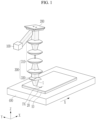
- FIG. 1 is a schematic perspective view of the digital exposure system according to the exemplary embodiment of the present invention
- FIG. 2 is a schematic front view of the digital exposure system according to the exemplary embodiment of the present invention
- FIG. 3 is a schematic side view of the digital exposure system according to the exemplary embodiment of the present invention.
- the digital exposure system includes a light source 100, a digital mirror device 200, an optical system 300, and a substrate scanner 400.
- the light source 100 may radiate light 1 onto a photosensitive layer 20 on a substrate 20.
- the light source 100 may include any one selected from LEDs, lamps, lasers, and the like.
- Light 1 which is radiated from the light source 100 may have various wavelengths of 365 nm, 435 nm, 405 nm, and the like. This light 1 which is radiated from the light source 100 may enter the digital mirror device 200 via a reflective member 30.
- the digital mirror device 200 may selectively transmit the light 1 emitted from the light source 100 to form a two-dimensional pattern image PI.
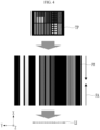
- FIG. 4 is a view for explaining a situation in which the digital exposure system according to the exemplary embodiment of the present invention forms a two-dimensional pattern image and modulates the two-dimensional pattern image into a one-dimensional pattern image.
- a two-dimensional pattern image PI which is generated by the digital mirror device 200 may have a uniform image in a direction X parallel with a scan direction X for a substrate 10 and have an image of a target pattern TP in a direction Y perpendicular to the scan direction X for the substrate 10.
- the optical system 300 may modulate the two-dimensional pattern image PI, generated by the digital mirror device 200, into a one-dimensional pattern image LI.
- the one-dimensional pattern image LI may have an image of the target pattern TP only in the direction Y perpendicular to the scan direction X for the substrate 10.
- the optical system 300 may include a plurality of projection lenses 310, and a cylindrical lens 320 that is positioned on a light path between the projection lenses 310 and the substrate 10.
- the cylindrical lens 320 is an asymmetric lens, and by the optical system 300 including the asymmetric lens, the two-dimensional pattern image PI may be focused in the direction X parallel with the scan direction X for the substrate 10, imaged in the direction Y perpendicular to the scan direction X for the substrate 10, and modulated into the one-dimensional pattern image LI.
- the focusing direction FA in which the two-dimensional pattern image PI is focused may be parallel with the scan direction X for the substrate 10. Accordingly, it is possible to project the one-dimensional pattern image LI with uniform light intensity onto the photosensitive layer 20 on the substrate 10.
- the substrate scanner 400 may adjust the position of the substrate 10 such that the one-dimensional pattern image LI is continuously projected onto the photosensitive layer 20 on the substrate 10 for scan exposure.
- the digital mirror device 200 may change the one-dimensional pattern image LI at a rate equal to the moving speed of the substrate 10 in sync with the moving speed of the substrate 10, such that the desired target pattern TP is projected onto the photosensitive layer 20 of the substrate 10.
- the digital exposure system may form the two-dimensional pattern image, which has a uniform image in a direction parallel with the substrate scan direction and has an image of the target pattern in a direction perpendicular to the substrate scan direction, by the digital mirror device, and project the desired target pattern TP onto the photosensitive layer 20 of the substrate 10 by the optical system by modulating the two-dimensional pattern image into the one-dimensional pattern image LI and changing the one-dimensional pattern image LI at a rate equal to the moving speed of the substrate 10. Accordingly, since the one-dimensional pattern image LI is continuously projected onto the photosensitive layer 20 of the substrate 10 for scan exposure, it is possible to apply the digital exposure system to a scan type of digital exposure process to improve the productivity.
- a diffraction compensator capable of compensating for light which is diffracted in the substrate scan direction is additionally included, unlike the above-mentioned exemplary embodiment.
- FIG. 5 is a schematic perspective view of a digital exposure system according to another exemplary embodiment of the present invention
- FIG. 6 is a schematic front view of the digital exposure system according to another exemplary embodiment of the present invention
- FIG. 7 is a schematic side view of the digital exposure system according to another exemplary embodiment of the present invention.
- FIGS. 5 to 7 Another exemplary embodiment shown in FIGS. 5 to 7 is substantially identical to the exemplary embodiment shown in FIGS. 1 to 4 except for a diffraction compensator, and thus a redundant description will not be made.
- the digital exposure system includes a light source 100, a digital mirror device 200, an optical system 300, a substrate scanner 400, and a diffraction compensator 500.
- the diffraction compensator 500 may be installed in the optical system 300 to compensate for light which is diffracted in the scan direction X for a substrate 10.
- the light source 100 uses a coherent light source such as a laser
- light 1 passing through the digital mirror device is diffracted, whereby diffracted light 2 is generated.
- the light may be defocused, thereby causing multiple images to be formed.
- the diffraction compensator 500 may be used to block the zero-order or higher order diffracted light 2 to form a clear one-dimensional linear image.
- the diffraction compensator 500 may be positioned between the plurality of projection lenses 310. This diffraction compensator 500 may be installed so as to correspond to a focusing point FP between the plurality of projection lenses 310 on which the light 1 is focused.
- the diffraction compensator 500 may include a slit extending in the direction Y perpendicular to the scan direction X for the substrate 10. Accordingly, it is possible to block high-order diffracted light diffracting in the scan direction X for the substrate 10 to form a clear one-dimensional linear image.
- the diffraction compensator 500 may not necessarily be limited thereto, and the diffraction compensator 500 may include an iris.
- the iris may block not only high-order diffracted light diffracting in the scan direction X for the substrate 10 but also high-order diffracted light diffracting in the direction Y perpendicular to the scan direction X for the substrate 10.
- the digital mirror device is disposed such that the two-dimensional pattern image focusing direction and the substrate scan direction are parallel with each other; however, other exemplary embodiments are possible in which a digital mirror device is disposed such that a two-dimensional pattern image focusing direction and a substrate scan direction have a predetermined inclination angle.
- FIGS. 8 and 9 a digital exposure system according to another exemplary embodiment of the present invention will be described in detail with reference to FIGS. 8 and 9 .
- FIG. 8 is a view for explaining a state where the two-dimensional pattern image focusing direction and substrate scan direction of the digital exposure system according to the exemplary embodiment of the present invention are parallel with each other
- FIG. 9 is a view for explaining a state where the two-dimensional pattern image focusing direction and substrate scan direction of the digital exposure system according to another exemplary embodiment of the present invention have a first inclination angle larger than 0° and smaller than 45°.
- FIG. 9 Another exemplary embodiment shown in FIG. 9 is substantially identical to the exemplary embodiment shown in FIGS. 1 to 4 and FIG. 8 except for the orientation of a digital mirror device, and thus a redundant description will not be made.
- the focusing direction FA in which two-dimensional pattern images PI1 and PI2 are focused and the scan direction X for a substrate 10 may be parallel with each other.
- pixels which are on and pixels which are off are clearly separated in each of a one-dimensional pattern image LI1 in the first row and a one-dimensional pattern image LI2 in the second row, it is difficult to project a continuous target pattern.
- the digital mirror device 200 may be disposed such that the focusing direction FA in which the two-dimensional pattern images PI1 and PI2 are focused and the scan direction X for the substrate 10 have a first inclination angle q1 larger than 0° and smaller than 45°.
- the focusing direction FA in which the two-dimensional pattern images PI1 and PI2 are focused and the scan direction X for the substrate 10 have a first inclination angle q1 larger than 0° and smaller than 45°.
- a digital mirror device is disposed such that a focusing direction in which a two-dimensional pattern image is focused and the pixel rotation axis of the digital mirror device are parallel with each other, unlike another exemplary embodiment shown in FIGS. 5 to 7 .
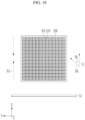
- FIG. 10 is a view for explaining a state where the two-dimensional pattern image focusing direction of a digital exposure system according to another exemplary embodiment of the present invention and the pixel rotation axis of a digital mirror device are perpendicular to each other
- FIG. 11 is a view for explaining a state where the two-dimensional pattern image focusing direction of a digital exposure system according to another exemplary embodiment of the present invention and the pixel rotation axis of a digital mirror device are parallel with each other.
- FIG. 11 Another exemplary embodiment shown in FIG. 11 is substantially identical to another exemplary embodiment shown in FIGS. 5 to 7 except for the orientation of a digital mirror device, and thus, a redundant description will not be made.
- a digital mirror device 200 of a digital exposure system may include a plurality of pixel mirrors 210 which rotates on a pixel rotation axis RA.
- the digital mirror device 200 may reflect light by rotating the plurality of pixel mirrors 210 arranged in a matrix on the pixel rotation axis RA, thereby forming a two-dimensional pattern image PI.
- the focusing direction FA of the two-dimensional pattern image PI and the scan direction X for a substrate 10 are parallel with each other, the focusing direction FA of the two-dimensional pattern image PI and the pixel rotation axis RA may have a second inclination angle q2 with respect to each other by the orientations of the digital mirror device 200 and the substrate 10.
- a step may occur between the plurality of pixel mirrors 210, resulting in a degradation in the clarity of one-dimensional pattern images LI.
- the focusing direction FA of a two-dimensional pattern image PI of a digital exposure system according to another exemplary embodiment of the present invention and the scan direction X for a substrate 10 are parallel with each other
- the focusing direction FA of the two-dimensional pattern image PI and the pixel rotation axis RA may be parallel with each other.
- any step does not occur between the plurality of pixel mirrors 210, the clarity of one-dimensional pattern images LI can be improved.
- the digital exposure system since the digital exposure system according to another exemplary embodiment of the present invention includes the diffraction compensator 500, it is possible to block the zero-order or higher order diffracted light 2 to form clear one-dimensional linear images.
- high-order diffracted light 2 caused by some of the plurality of pixel mirrors 210 is blocked by the diffraction compensator 500, it is possible to use only the pixel mirrors 210 positioned in the center area UA among the plurality of pixel mirrors 210. Accordingly, of light which is emitted from the light source 100, only light corresponding to the pixel mirrors 210 positioned in the center area UA may be emitted. Therefore, it is possible to minimize the exposure energy to be used.
- a digital mirror device is disposed such that while a two-dimensional pattern image focusing direction and a substrate scan direction have a first inclination angle larger than 0° and smaller than 45°, a focusing direction in which a two-dimensional pattern image is focused and the pixel rotation axis of the digital mirror device have the first inclination angle, unlike another exemplary embodiment shown in FIG. 11 .
- FIG. 12 is a view for explaining a state where while the two-dimensional pattern image focusing direction and substrate scan direction of a digital exposure system according to another exemplary embodiment of the present invention have the first inclination angle larger than 0° and smaller than 45°, the two-dimensional pattern image focusing direction and the pixel rotation axis of the digital mirror device have the first inclination angle.
- FIG. 12 Another exemplary embodiment shown in FIG. 12 is substantially identical to another exemplary embodiment shown in FIG. 11 except for the orientation of a digital mirror device, and thus a redundant description will not be made.
- the focusing direction FA of a two-dimensional pattern image PI of a digital exposure system according to an exemplary embodiment of the present invention and a scan direction X for a substrate 10 may have a first inclination angle q1 larger than 0° and smaller than 45°.
- pixels which are on and pixels which are off may be connected to each other without being clearly separated from each other in adjacent one-dimensional pattern images LI. Therefore, it is also possible to project a continuous target pattern.
- the focusing direction FA of the two-dimensional pattern image PI and the pixel rotation axis RA of the digital mirror device may have the first inclination angle q1.
- a step is minimized between the plurality of pixel mirrors 210, it is possible to minimize a degradation in the clarity of one-dimensional pattern images LI.
Landscapes
- Physics & Mathematics (AREA)
- General Physics & Mathematics (AREA)
- Exposure And Positioning Against Photoresist Photosensitive Materials (AREA)
Abstract
Description
- The present invention relates to a digital exposure system, and more particularly, to a digital exposure system using a digital mirror device.
- In general, a digital exposure process is a type of photolithography and is a technology for creating a desired pattern with a photoresist without a mask. This digital exposure process creates a pattern by reproducing pattern images by a digital device and projecting the pattern images onto a substrate by an imaging optical system such that a photosensitive material applied to the substrate is exposed to light. In this case, since the sizes of pattern images are smaller than the size of the substrate, a desired pattern is created over the entire substrate by performing the exposure process while changing the pattern images for individual positions of the substrate.
- Digital exposure systems using digital devices such as digital mirror devices (DMDs) or spatial light modulators (SLMs) perform exposure processes by projecting two-dimensional pattern images formed by the digital mirror devices (DMDs) onto substrates through optical systems. Therefore, digital exposure systems using digital mirror devices (DMDs) are optimized for a step-and-repeat type of exposure processes due to the advantage of being able to project a two-dimensional pattern image at one time, and are actively applied to 3D printers and the like.
- However, since the digital exposure systems using the digital mirror devices (DMDs) project a two-dimensional pattern image at one time, they are not suitable for a scan type of exposure processes. A roll-to-roll exposure process is an exposure method for continuously producing flexible substrates, and performs continuous exposure while transferring a flexible substrate rolled in the form of a roll. However, since the digital exposure systems using the digital mirror devices are optimized for the step-and-repeat type of exposure processes, it is difficult to apply them to a roll-to-roll exposure process of performing scan exposure while continuously transferring a roll. In addition, since the roll-to-roll exposure process is a method of performing exposure while transferring a flexible substrate having the form of a roll, in order to improve the accuracy of exposure, it is required to minimize deformation and vibration of rolls which are transferred, so the exposure process should be performed on the surface of a roll transfer drum where vibration of rolls is minimized. Therefore, it is difficult to apply the digital exposure systems using the digital mirror devices for projecting two-dimensional planar images for exposure to the roll-to-roll exposure process. In addition, since they project a two-dimensional pattern image at one time, it is difficult for them to cope with the curvatures of substrate surfaces. For this reason, it is difficult to apply the digital exposure systems using the digital mirror devices (DMDs) to exposure processes for high-performance semiconductor packages such as wafer level packages (WLPs) or panel level packages (PLPs) in which severe substrate warpage may occur.
- The present invention attempts to solve the above-mentioned problems of the related art and provide a digital exposure system capable of performing digital exposure on a non-planar substrate in a scanning manner.
- A digital exposure system according to an exemplary embodiment of the present invention includes a light source that radiates light onto a substrate, a digital mirror device that forms a two-dimensional pattern image by selectively transmitting light emitted from the light source, an optical system that modulates the two-dimensional pattern image into a one-dimensional pattern image, and a substrate scanner that adjusts the position of the substrate to continuously project the one-dimensional pattern image onto a photosensitive layer on the substrate for scan exposure, and the two-dimensional pattern image has a uniform image in a direction parallel with a scan direction for the substrate and has an image of a target pattern in a direction perpendicular to the scan direction for the substrate.
- Further, the optical system may include a plurality of projection lenses, and a cylindrical lens that is positioned between the projection lenses and the substrate.
- Furthermore, the two-dimensional pattern image may be focused in the direction parallel with the scan direction for the substrate, imaged in the direction perpendicular to the scan direction for the substrate, and modulated into the one-dimensional pattern image.
- Also, the digital exposure system may further include a diffraction compensator that is installed in the optical system to compensate for light which is diffracted in the scan direction for the substrate.
- Further, the diffraction compensator may be positioned between the plurality of projection lenses of the optical system.
- Furthermore, the diffraction compensator may be installed so as to correspond to a focusing point between the plurality of projection lenses on which the light is focused.
- Also, the diffraction compensator may include a slit or an iris.
- Further, a focusing direction in which the two-dimensional pattern image is focused and the scan direction for the substrate may have a first inclination angle larger than 0° and smaller than 45°.
- Furthermore, the digital mirror device may include a plurality of pixel mirrors which rotates on a pixel rotation axis, and the focusing direction in which the two-dimensional pattern image is focused and the pixel rotation axis may be parallel with each other.
- In addition, the digital mirror device may include a plurality of pixel mirrors which rotates on a pixel rotation axis, and the focusing direction in which the two-dimensional pattern image is focused and the pixel rotation axis may have the first inclination angle.
- The digital exposure system according to the exemplary embodiment of the present invention forms a two-dimensional pattern image, which has a uniform image in a substrate scan direction and has an image of a target pattern in a direction perpendicular to the substrate scan direction, by the digital mirror device, and modulates the two-dimensional pattern image into a one-dimensional pattern image by the optical system, and continuously projects the one-dimensional pattern image for scan exposure. Therefore, it can be applied to a scan type of digital exposure process to improve the productivity. Accordingly, the digital exposure system can be applied to a roll-to-roll type of digital exposure process.
- Further, since it is possible to form a pattern on a substrate by continuously projecting a one-dimensional pattern image for scan exposure, it is possible to apply a digital exposure process to non-planar substrates.
-
-
FIG. 1 is a schematic perspective view of a digital exposure system according to an exemplary embodiment of the present invention. -
FIG. 2 is a schematic front view of the digital exposure system according to the exemplary embodiment of the present invention. -
FIG. 3 is a schematic side view of the digital exposure system according to the exemplary embodiment of the present invention. -
FIG. 4 is a view for explaining a situation in which the digital exposure system according to the exemplary embodiment of the present invention forms a two-dimensional pattern image and modulates the two-dimensional pattern image into a one-dimensional pattern image. -
FIG. 5 is a schematic perspective view of a digital exposure system according to another exemplary embodiment of the present invention. -
FIG. 6 is a schematic front view of the digital exposure system according to another exemplary embodiment of the present invention. -
FIG. 7 is a schematic side view of the digital exposure system according to another exemplary embodiment of the present invention. -
FIG. 8 is a view for explaining a state where the two-dimensional pattern image focusing direction and substrate scan direction of the digital exposure system according to the exemplary embodiment of the present invention are parallel with each other. -
FIG. 9 is a view for explaining a state where the two-dimensional pattern image focusing direction and substrate scan direction of a digital exposure system according to another exemplary embodiment of the present invention have a first inclination angle larger than 0° and smaller than 45°. -
FIG. 10 is a view for explaining a state where the two-dimensional pattern image focusing direction of a digital exposure system according to another exemplary embodiment of the present invention and the pixel rotation axis of a digital mirror device are perpendicular to each other. -
FIG. 11 is a view for explaining a state where the two-dimensional pattern image focusing direction of a digital exposure system according to another exemplary embodiment of the present invention and the pixel rotation axis of a digital mirror device are parallel with each other. -
FIG. 12 is a view for explaining a state where while the two-dimensional pattern image focusing direction and substrate scan direction of a digital exposure system according to another exemplary embodiment of the present invention have the first inclination angle larger than 0° and smaller than 45°, the two-dimensional pattern image focusing direction and the pixel rotation axis of the digital mirror device have the first inclination angle. - In the following detailed description, only certain exemplary embodiments of the present invention have been shown and described, simply by way of illustration. The present invention can be variously implemented and is not limited to the following exemplary embodiments.
- The drawings and description are to be regarded as illustrative in nature and not restrictive. Like reference numerals designate like elements throughout the specification.
- Now, a digital exposure system according to an exemplary embodiment of the present invention will be described in detail with reference to
FIGS. 1 to 3 . -
FIG. 1 is a schematic perspective view of the digital exposure system according to the exemplary embodiment of the present invention,FIG. 2 is a schematic front view of the digital exposure system according to the exemplary embodiment of the present invention, andFIG. 3 is a schematic side view of the digital exposure system according to the exemplary embodiment of the present invention. - As shown in
FIGS. 1 to 3 , the digital exposure system according to the exemplary embodiment of the present invention includes alight source 100, adigital mirror device 200, anoptical system 300, and asubstrate scanner 400. - The
light source 100 may radiatelight 1 onto aphotosensitive layer 20 on asubstrate 20. Thelight source 100 may include any one selected from LEDs, lamps, lasers, and the like.Light 1 which is radiated from thelight source 100 may have various wavelengths of 365 nm, 435 nm, 405 nm, and the like. Thislight 1 which is radiated from thelight source 100 may enter thedigital mirror device 200 via areflective member 30. - The
digital mirror device 200 may selectively transmit thelight 1 emitted from thelight source 100 to form a two-dimensional pattern image PI. -
FIG. 4 is a view for explaining a situation in which the digital exposure system according to the exemplary embodiment of the present invention forms a two-dimensional pattern image and modulates the two-dimensional pattern image into a one-dimensional pattern image. - As shown in
FIG. 4 , a two-dimensional pattern image PI which is generated by thedigital mirror device 200 may have a uniform image in a direction X parallel with a scan direction X for asubstrate 10 and have an image of a target pattern TP in a direction Y perpendicular to the scan direction X for thesubstrate 10. - The
optical system 300 may modulate the two-dimensional pattern image PI, generated by thedigital mirror device 200, into a one-dimensional pattern image LI. The one-dimensional pattern image LI may have an image of the target pattern TP only in the direction Y perpendicular to the scan direction X for thesubstrate 10. - The
optical system 300 may include a plurality ofprojection lenses 310, and acylindrical lens 320 that is positioned on a light path between theprojection lenses 310 and thesubstrate 10. Thecylindrical lens 320 is an asymmetric lens, and by theoptical system 300 including the asymmetric lens, the two-dimensional pattern image PI may be focused in the direction X parallel with the scan direction X for thesubstrate 10, imaged in the direction Y perpendicular to the scan direction X for thesubstrate 10, and modulated into the one-dimensional pattern image LI. Here, the focusing direction FA in which the two-dimensional pattern image PI is focused may be parallel with the scan direction X for thesubstrate 10. Accordingly, it is possible to project the one-dimensional pattern image LI with uniform light intensity onto thephotosensitive layer 20 on thesubstrate 10. - The
substrate scanner 400 may adjust the position of thesubstrate 10 such that the one-dimensional pattern image LI is continuously projected onto thephotosensitive layer 20 on thesubstrate 10 for scan exposure. At this time, thedigital mirror device 200 may change the one-dimensional pattern image LI at a rate equal to the moving speed of thesubstrate 10 in sync with the moving speed of thesubstrate 10, such that the desired target pattern TP is projected onto thephotosensitive layer 20 of thesubstrate 10. - As described above, the digital exposure system according to the exemplary embodiment of the present invention may form the two-dimensional pattern image, which has a uniform image in a direction parallel with the substrate scan direction and has an image of the target pattern in a direction perpendicular to the substrate scan direction, by the digital mirror device, and project the desired target pattern TP onto the
photosensitive layer 20 of thesubstrate 10 by the optical system by modulating the two-dimensional pattern image into the one-dimensional pattern image LI and changing the one-dimensional pattern image LI at a rate equal to the moving speed of thesubstrate 10. Accordingly, since the one-dimensional pattern image LI is continuously projected onto thephotosensitive layer 20 of thesubstrate 10 for scan exposure, it is possible to apply the digital exposure system to a scan type of digital exposure process to improve the productivity. Accordingly, since it is possible to form a linear focus on the surface of a cylindrical drum for a roll-to-roll type of digital exposure process, it is possible to apply the digital exposure system to a roll-to-roll exposure process required to perform exposure on a curved surface. - Also, since it is a linear scan exposure process, rather than a step-and-repeat type of exposure process, it is possible to more accurately correct the pattern in real time for each scan position. Accordingly, it is also possible to apply the digital exposure system to exposure processes for high-performance semiconductor packages such as wafer level packages (WLPs) or panel level packages (PLPs) in which severe substrate warpage may occur.
- Meanwhile, other exemplary embodiments are possible in which a diffraction compensator capable of compensating for light which is diffracted in the substrate scan direction is additionally included, unlike the above-mentioned exemplary embodiment.
- Hereinafter, a digital exposure system according to another exemplary embodiment of the present invention will be described in detail with reference to
FIGS. 5 to 7 . -
FIG. 5 is a schematic perspective view of a digital exposure system according to another exemplary embodiment of the present invention,FIG. 6 is a schematic front view of the digital exposure system according to another exemplary embodiment of the present invention, andFIG. 7 is a schematic side view of the digital exposure system according to another exemplary embodiment of the present invention. - Another exemplary embodiment shown in
FIGS. 5 to 7 is substantially identical to the exemplary embodiment shown inFIGS. 1 to 4 except for a diffraction compensator, and thus a redundant description will not be made. - As shown in
FIGS. 5 to 7 , the digital exposure system according to another exemplary embodiment of the present invention includes alight source 100, adigital mirror device 200, anoptical system 300, asubstrate scanner 400, and adiffraction compensator 500. - The
diffraction compensator 500 may be installed in theoptical system 300 to compensate for light which is diffracted in the scan direction X for asubstrate 10. - When the
light source 100 uses a coherent light source such as a laser, light 1 passing through the digital mirror device is diffracted, whereby diffractedlight 2 is generated. Accordingly, the light may be defocused, thereby causing multiple images to be formed. For this reason, thediffraction compensator 500 may be used to block the zero-order or higher order diffracted light 2 to form a clear one-dimensional linear image. - The
diffraction compensator 500 may be positioned between the plurality ofprojection lenses 310. Thisdiffraction compensator 500 may be installed so as to correspond to a focusing point FP between the plurality ofprojection lenses 310 on which thelight 1 is focused. - The
diffraction compensator 500 may include a slit extending in the direction Y perpendicular to the scan direction X for thesubstrate 10. Accordingly, it is possible to block high-order diffracted light diffracting in the scan direction X for thesubstrate 10 to form a clear one-dimensional linear image. - However, the
diffraction compensator 500 may not necessarily be limited thereto, and thediffraction compensator 500 may include an iris. The iris may block not only high-order diffracted light diffracting in the scan direction X for thesubstrate 10 but also high-order diffracted light diffracting in the direction Y perpendicular to the scan direction X for thesubstrate 10. - Meanwhile, in the above-mentioned exemplary embodiment, the digital mirror device is disposed such that the two-dimensional pattern image focusing direction and the substrate scan direction are parallel with each other; however, other exemplary embodiments are possible in which a digital mirror device is disposed such that a two-dimensional pattern image focusing direction and a substrate scan direction have a predetermined inclination angle.
- Hereinafter, a digital exposure system according to another exemplary embodiment of the present invention will be described in detail with reference to
FIGS. 8 and9 . -
FIG. 8 is a view for explaining a state where the two-dimensional pattern image focusing direction and substrate scan direction of the digital exposure system according to the exemplary embodiment of the present invention are parallel with each other, andFIG. 9 is a view for explaining a state where the two-dimensional pattern image focusing direction and substrate scan direction of the digital exposure system according to another exemplary embodiment of the present invention have a first inclination angle larger than 0° and smaller than 45°. - Another exemplary embodiment shown in
FIG. 9 is substantially identical to the exemplary embodiment shown inFIGS. 1 to 4 andFIG. 8 except for the orientation of a digital mirror device, and thus a redundant description will not be made. - As shown in
FIG. 8 , in the digital exposure system according to the exemplary embodiment of the present invention, the focusing direction FA in which two-dimensional pattern images PI1 and PI2 are focused and the scan direction X for asubstrate 10 may be parallel with each other. In this case, since pixels which are on and pixels which are off are clearly separated in each of a one-dimensional pattern image LI1 in the first row and a one-dimensional pattern image LI2 in the second row, it is difficult to project a continuous target pattern. - However, as shown in
FIG. 9 , in the digital exposure system according to another exemplary embodiment of the present invention, thedigital mirror device 200 may be disposed such that the focusing direction FA in which the two-dimensional pattern images PI1 and PI2 are focused and the scan direction X for thesubstrate 10 have a first inclination angle q1 larger than 0° and smaller than 45°. In this case, since pixels which are on and pixels which are off are connected to each other without being clearly separated from each other in each of a one-dimensional pattern image LI1 in the first row and a one-dimensional pattern image LI2 in the second row, it is also possible to project a continuous target pattern. - Meanwhile, other exemplary embodiments are possible in which a digital mirror device is disposed such that a focusing direction in which a two-dimensional pattern image is focused and the pixel rotation axis of the digital mirror device are parallel with each other, unlike another exemplary embodiment shown in
FIGS. 5 to 7 . - Hereinafter, digital exposure systems according to other exemplary embodiments of the present invention will be described in detail with reference to
FIGS. 10 and11 . -
FIG. 10 is a view for explaining a state where the two-dimensional pattern image focusing direction of a digital exposure system according to another exemplary embodiment of the present invention and the pixel rotation axis of a digital mirror device are perpendicular to each other, andFIG. 11 is a view for explaining a state where the two-dimensional pattern image focusing direction of a digital exposure system according to another exemplary embodiment of the present invention and the pixel rotation axis of a digital mirror device are parallel with each other. - Another exemplary embodiment shown in
FIG. 11 is substantially identical to another exemplary embodiment shown inFIGS. 5 to 7 except for the orientation of a digital mirror device, and thus, a redundant description will not be made. - As shown in
FIG. 10 , adigital mirror device 200 of a digital exposure system according to an exemplary embodiment of the present invention may include a plurality of pixel mirrors 210 which rotates on a pixel rotation axis RA. Thedigital mirror device 200 may reflect light by rotating the plurality of pixel mirrors 210 arranged in a matrix on the pixel rotation axis RA, thereby forming a two-dimensional pattern image PI. - In this case, when the focusing direction FA of the two-dimensional pattern image PI and the scan direction X for a
substrate 10 are parallel with each other, the focusing direction FA of the two-dimensional pattern image PI and the pixel rotation axis RA may have a second inclination angle q2 with respect to each other by the orientations of thedigital mirror device 200 and thesubstrate 10. In this case, a step may occur between the plurality of pixel mirrors 210, resulting in a degradation in the clarity of one-dimensional pattern images LI. - However, as shown in
FIG. 11 , when the focusing direction FA of a two-dimensional pattern image PI of a digital exposure system according to another exemplary embodiment of the present invention and the scan direction X for asubstrate 10 are parallel with each other, the focusing direction FA of the two-dimensional pattern image PI and the pixel rotation axis RA may be parallel with each other. In this case, since any step does not occur between the plurality of pixel mirrors 210, the clarity of one-dimensional pattern images LI can be improved. - Further, since the digital exposure system according to another exemplary embodiment of the present invention includes the
diffraction compensator 500, it is possible to block the zero-order or higher order diffracted light 2 to form clear one-dimensional linear images. In this case, since high-order diffracted light 2 caused by some of the plurality of pixel mirrors 210 is blocked by thediffraction compensator 500, it is possible to use only the pixel mirrors 210 positioned in the center area UA among the plurality of pixel mirrors 210. Accordingly, of light which is emitted from thelight source 100, only light corresponding to the pixel mirrors 210 positioned in the center area UA may be emitted. Therefore, it is possible to minimize the exposure energy to be used. - Meanwhile, other exemplary embodiments are possible in which a digital mirror device is disposed such that while a two-dimensional pattern image focusing direction and a substrate scan direction have a first inclination angle larger than 0° and smaller than 45°, a focusing direction in which a two-dimensional pattern image is focused and the pixel rotation axis of the digital mirror device have the first inclination angle, unlike another exemplary embodiment shown in
FIG. 11 . - Hereinafter, a digital exposure system according to another exemplary embodiment of the present invention will be described in detail with reference to
FIG. 12 . -
FIG. 12 is a view for explaining a state where while the two-dimensional pattern image focusing direction and substrate scan direction of a digital exposure system according to another exemplary embodiment of the present invention have the first inclination angle larger than 0° and smaller than 45°, the two-dimensional pattern image focusing direction and the pixel rotation axis of the digital mirror device have the first inclination angle. - Another exemplary embodiment shown in
FIG. 12 is substantially identical to another exemplary embodiment shown inFIG. 11 except for the orientation of a digital mirror device, and thus a redundant description will not be made. - As shown in
FIG. 12 , the focusing direction FA of a two-dimensional pattern image PI of a digital exposure system according to an exemplary embodiment of the present invention and a scan direction X for asubstrate 10 may have a first inclination angle q1 larger than 0° and smaller than 45°. In this case, pixels which are on and pixels which are off may be connected to each other without being clearly separated from each other in adjacent one-dimensional pattern images LI. Therefore, it is also possible to project a continuous target pattern. - Also, the focusing direction FA of the two-dimensional pattern image PI and the pixel rotation axis RA of the digital mirror device may have the first inclination angle q1. In this case, since a step is minimized between the plurality of pixel mirrors 210, it is possible to minimize a degradation in the clarity of one-dimensional pattern images LI.
- While this invention has been described in connection with what is presently considered to be practical exemplary embodiments, those skilled in the art will easily understood that the invention is not limited to the disclosed exemplary embodiments, and it is possible to make various modifications and equivalent arrangements without departing from the scope of the appended claims.
<Description of symbols> *64100: Light source 200: Digital mirror device 210: Pixel mirror 300: Optical system 400: Substrate scanner 500: Diffraction compensator
Claims (10)
- A digital exposure system comprising:a light source that radiates light onto a substrate;a digital mirror device that forms a two-dimensional pattern image by selectively transmitting light emitted from the light source;an optical system that modulates the two-dimensional pattern image into a one-dimensional pattern image; anda substrate scanner that adjusts the position of the substrate to continuously project the one-dimensional pattern image onto a photosensitive layer on the substrate for scan exposure,wherein the two-dimensional pattern image has a uniform image in a direction parallel with a scan direction for the substrate and has an image of a target pattern in a direction perpendicular to the scan direction for the substrate.
- The digital exposure system of claim 1, wherein:
the optical system includes the following:a plurality of projection lenses; anda cylindrical lens that is positioned between the projection lenses and the substrate. - The digital exposure system of claim 2, wherein:
the two-dimensional pattern image is focused in the direction parallel with the scan direction for the substrate, imaged in the direction perpendicular to the scan direction for the substrate, and modulated into the one-dimensional pattern image. - The digital exposure system of claim 3, further comprising:
a diffraction compensator that is installed in the optical system to compensate for light which is diffracted in the scan direction for the substrate. - The digital exposure system of claim 4, wherein:
the diffraction compensator is positioned between the plurality of projection lenses of the optical system. - The digital exposure system of claim 5, wherein:
the diffraction compensator is installed so as to correspond to a focusing point between the plurality of projection lenses on which the light is focused. - The digital exposure system of claim 4, wherein:
the diffraction compensator includes a slit or an iris. - The digital exposure system of claim 4, wherein:
a focusing direction in which the two-dimensional pattern image is focused and the scan direction for the substrate have a first inclination angle larger than 0° and smaller than 45°. - The digital exposure system of claim 8, wherein:the digital mirror device includes a plurality of pixel mirrors which rotates on a pixel rotation axis, andthe focusing direction in which the two-dimensional pattern image is focused and the pixel rotation axis are parallel with each other.
- The digital exposure system of claim 8, wherein:the digital mirror device includes a plurality of pixel mirrors which rotates on a pixel rotation axis, andthe focusing direction in which the two-dimensional pattern image is focused and the pixel rotation axis have the first inclination angle.
Applications Claiming Priority (2)
| Application Number | Priority Date | Filing Date | Title |
|---|---|---|---|
| KR1020220032884A KR102741727B1 (en) | 2022-03-16 | 2022-03-16 | Digital exposure system |
| PCT/KR2022/018248 WO2023177039A1 (en) | 2022-03-16 | 2022-11-17 | Digital exposure system |
Publications (2)
| Publication Number | Publication Date |
|---|---|
| EP4495690A1 true EP4495690A1 (en) | 2025-01-22 |
| EP4495690A4 EP4495690A4 (en) | 2026-03-11 |
Family
ID=88023553
Family Applications (1)
| Application Number | Title | Priority Date | Filing Date |
|---|---|---|---|
| EP22932406.6A Pending EP4495690A4 (en) | 2022-03-16 | 2022-11-17 | DIGITAL LIGHTING SYSTEM |
Country Status (5)
| Country | Link |
|---|---|
| US (1) | US20250028247A1 (en) |
| EP (1) | EP4495690A4 (en) |
| JP (1) | JP7764629B2 (en) |
| KR (1) | KR102741727B1 (en) |
| WO (1) | WO2023177039A1 (en) |
Family Cites Families (15)
| Publication number | Priority date | Publication date | Assignee | Title |
|---|---|---|---|---|
| JP3718397B2 (en) | 2000-01-07 | 2005-11-24 | ペンタックス株式会社 | Multi-beam optical system |
| JP2001330912A (en) * | 2000-05-18 | 2001-11-30 | Fuji Photo Film Co Ltd | Image recording device |
| US6493867B1 (en) | 2000-08-08 | 2002-12-10 | Ball Semiconductor, Inc. | Digital photolithography system for making smooth diagonal components |
| WO2005081034A1 (en) | 2004-02-25 | 2005-09-01 | Nikon Corporation | Two-dimensional light modulation device, exposure apparatus, and exposure method |
| KR20070078241A (en) * | 2006-01-26 | 2007-07-31 | (주)하드램 | High precision exposure device using micro mirror array |
| US8115904B2 (en) * | 2008-05-30 | 2012-02-14 | Corning Incorporated | Illumination system for sizing focused spots of a patterning system for maskless lithography |
| US8531648B2 (en) * | 2008-09-22 | 2013-09-10 | Asml Netherlands B.V. | Lithographic apparatus, programmable patterning device and lithographic method |
| WO2010075158A1 (en) * | 2008-12-23 | 2010-07-01 | 3M Innovative Properties Company | Roll-to-roll digital photolithography |
| US8872875B2 (en) * | 2011-08-24 | 2014-10-28 | Palo Alto Research Center Incorporated | Single-pass imaging system with anamorphic optical system |
| US8472104B2 (en) * | 2011-08-24 | 2013-06-25 | Palo Alto Research Center Incorporated | Single-pass imaging system using spatial light modulator anamorphic projection optics |
| JP6321189B2 (en) * | 2014-01-27 | 2018-05-09 | 東京エレクトロン株式会社 | System and method for shifting critical dimensions of patterned films |
| JP6546868B2 (en) | 2015-04-08 | 2019-07-17 | パロ アルト リサーチ センター インコーポレイテッド | VCSEL-based variable image beam generator |
| CN105259738A (en) * | 2015-11-09 | 2016-01-20 | 中国科学院上海光学精密机械研究所 | Parallel detection device for multiple field point wave aberrations of lithographic projection objective lens and detection method |
| SG11201908444RA (en) * | 2017-03-15 | 2019-10-30 | Callaghan Innovation | Apparatus for and method of manufacturing an article using photolithography and a photoresist |
| KR20190054815A (en) * | 2017-11-14 | 2019-05-22 | 삼성전자주식회사 | Maskless exposure method, maskless exposure apparatus and method of manufacturing a semiconductor device using the same |
-
2022
- 2022-03-16 KR KR1020220032884A patent/KR102741727B1/en active Active
- 2022-11-17 US US18/714,640 patent/US20250028247A1/en active Pending
- 2022-11-17 EP EP22932406.6A patent/EP4495690A4/en active Pending
- 2022-11-17 JP JP2024555225A patent/JP7764629B2/en active Active
- 2022-11-17 WO PCT/KR2022/018248 patent/WO2023177039A1/en not_active Ceased
Also Published As
| Publication number | Publication date |
|---|---|
| KR20230135422A (en) | 2023-09-25 |
| WO2023177039A1 (en) | 2023-09-21 |
| JP7764629B2 (en) | 2025-11-05 |
| KR102741727B1 (en) | 2024-12-11 |
| JP2025509789A (en) | 2025-04-11 |
| US20250028247A1 (en) | 2025-01-23 |
| EP4495690A4 (en) | 2026-03-11 |
Similar Documents
| Publication | Publication Date | Title |
|---|---|---|
| JP4079301B2 (en) | Optical imaging head with multiple writing beam source | |
| JP7023601B2 (en) | Direct imaging exposure equipment and direct imaging exposure method | |
| US8335999B2 (en) | System and method for optical shearing | |
| US9310697B2 (en) | Digital exposure device using digital micro-mirror device and a method for controlling the same | |
| JPH11320968A (en) | Optical image forming method and apparatus, imaging system and exposing unit for lithography | |
| JP4486323B2 (en) | Pixel position specifying method, image shift correcting method, and image forming apparatus | |
| US20120050705A1 (en) | Photolithography system | |
| US10761316B2 (en) | Illumination apparatus, optical apparatus, imprint apparatus, projection apparatus, and method of manufacturing article | |
| KR20090021755A (en) | Exposure apparatus and exposure method of semiconductor substrate | |
| US20250028247A1 (en) | Digital exposure system | |
| US5479289A (en) | Method and apparatus for preparing imaged light | |
| US7414701B2 (en) | Method and systems for total focus deviation adjustments on maskless lithography systems | |
| US7564535B2 (en) | Seamless exposure with projection system comprises array of micromirrors with predefined reflectivity variations | |
| JP4638826B2 (en) | Drawing apparatus and drawing method | |
| JP7090002B2 (en) | Exposure device | |
| KR100946247B1 (en) | Multiple exposure system for performing multiple exposures by beam movement | |
| JP5357617B2 (en) | Exposure equipment | |
| KR102845530B1 (en) | Digital exposure system | |
| WO2010044307A1 (en) | Illumination optical system, aligner, and process for fabricating device | |
| JP2024043177A (en) | Optical equipment, exposure equipment and exposure method | |
| CN116804797A (en) | Optical device, exposure device and exposure method | |
| JP7196271B2 (en) | Direct imaging exposure apparatus and direct imaging exposure method | |
| US12055858B2 (en) | Method and device for pattern generation | |
| WO2024053194A1 (en) | Light irradiation device and exposure device | |
| JP2001159742A (en) | Division exposure apparatus using hologram scanning system |
Legal Events
| Date | Code | Title | Description |
|---|---|---|---|
| STAA | Information on the status of an ep patent application or granted ep patent |
Free format text: STATUS: THE INTERNATIONAL PUBLICATION HAS BEEN MADE |
|
| PUAI | Public reference made under article 153(3) epc to a published international application that has entered the european phase |
Free format text: ORIGINAL CODE: 0009012 |
|
| STAA | Information on the status of an ep patent application or granted ep patent |
Free format text: STATUS: REQUEST FOR EXAMINATION WAS MADE |
|
| 17P | Request for examination filed |
Effective date: 20241001 |
|
| AK | Designated contracting states |
Kind code of ref document: A1 Designated state(s): AL AT BE BG CH CY CZ DE DK EE ES FI FR GB GR HR HU IE IS IT LI LT LU LV MC ME MK MT NL NO PL PT RO RS SE SI SK SM TR |
|
| DAV | Request for validation of the european patent (deleted) | ||
| DAX | Request for extension of the european patent (deleted) | ||
| A4 | Supplementary search report drawn up and despatched |
Effective date: 20260211 |
|
| RIC1 | Information provided on ipc code assigned before grant |
Ipc: G03F 7/20 20060101AFI20260205BHEP |