EP4492460A1 - Semiconductor module, power conversion device, and method for manufacturing semiconductor module - Google Patents
Semiconductor module, power conversion device, and method for manufacturing semiconductor module Download PDFInfo
- Publication number
- EP4492460A1 EP4492460A1 EP23766943.7A EP23766943A EP4492460A1 EP 4492460 A1 EP4492460 A1 EP 4492460A1 EP 23766943 A EP23766943 A EP 23766943A EP 4492460 A1 EP4492460 A1 EP 4492460A1
- Authority
- EP
- European Patent Office
- Prior art keywords
- semiconductor module
- semiconductor chip
- control pin
- case
- insulating substrate
- Prior art date
- Legal status (The legal status is an assumption and is not a legal conclusion. Google has not performed a legal analysis and makes no representation as to the accuracy of the status listed.)
- Pending
Links
Images


Classifications
-
- H—ELECTRICITY
- H10—SEMICONDUCTOR DEVICES; ELECTRIC SOLID-STATE DEVICES NOT OTHERWISE PROVIDED FOR
- H10W—GENERIC PACKAGES, INTERCONNECTIONS, CONNECTORS OR OTHER CONSTRUCTIONAL DETAILS OF DEVICES COVERED BY CLASS H10
- H10W72/00—Interconnections or connectors in packages
- H10W72/50—Bond wires
-
- H—ELECTRICITY
- H10—SEMICONDUCTOR DEVICES; ELECTRIC SOLID-STATE DEVICES NOT OTHERWISE PROVIDED FOR
- H10W—GENERIC PACKAGES, INTERCONNECTIONS, CONNECTORS OR OTHER CONSTRUCTIONAL DETAILS OF DEVICES COVERED BY CLASS H10
- H10W70/00—Package substrates; Interposers; Redistribution layers [RDL]
- H10W70/60—Insulating or insulated package substrates; Interposers; Redistribution layers
- H10W70/62—Insulating or insulated package substrates; Interposers; Redistribution layers characterised by their interconnections
- H10W70/65—Shapes or dispositions of interconnections
- H10W70/658—Shapes or dispositions of interconnections for devices provided for in groups H10D8/00 - H10D48/00
-
- H—ELECTRICITY
- H10—SEMICONDUCTOR DEVICES; ELECTRIC SOLID-STATE DEVICES NOT OTHERWISE PROVIDED FOR
- H10W—GENERIC PACKAGES, INTERCONNECTIONS, CONNECTORS OR OTHER CONSTRUCTIONAL DETAILS OF DEVICES COVERED BY CLASS H10
- H10W76/00—Containers; Fillings or auxiliary members therefor; Seals
- H10W76/10—Containers or parts thereof
- H10W76/12—Containers or parts thereof characterised by their shape
- H10W76/15—Containers comprising an insulating or insulated base
-
- H—ELECTRICITY
- H10—SEMICONDUCTOR DEVICES; ELECTRIC SOLID-STATE DEVICES NOT OTHERWISE PROVIDED FOR
- H10W—GENERIC PACKAGES, INTERCONNECTIONS, CONNECTORS OR OTHER CONSTRUCTIONAL DETAILS OF DEVICES COVERED BY CLASS H10
- H10W76/00—Containers; Fillings or auxiliary members therefor; Seals
- H10W76/10—Containers or parts thereof
- H10W76/12—Containers or parts thereof characterised by their shape
- H10W76/15—Containers comprising an insulating or insulated base
- H10W76/157—Containers comprising an insulating or insulated base having interconnections parallel to the insulating or insulated base
-
- H—ELECTRICITY
- H10—SEMICONDUCTOR DEVICES; ELECTRIC SOLID-STATE DEVICES NOT OTHERWISE PROVIDED FOR
- H10W—GENERIC PACKAGES, INTERCONNECTIONS, CONNECTORS OR OTHER CONSTRUCTIONAL DETAILS OF DEVICES COVERED BY CLASS H10
- H10W76/00—Containers; Fillings or auxiliary members therefor; Seals
- H10W76/40—Fillings or auxiliary members in containers, e.g. centering rings
- H10W76/42—Fillings
- H10W76/47—Solid or gel fillings
-
- H—ELECTRICITY
- H10—SEMICONDUCTOR DEVICES; ELECTRIC SOLID-STATE DEVICES NOT OTHERWISE PROVIDED FOR
- H10W—GENERIC PACKAGES, INTERCONNECTIONS, CONNECTORS OR OTHER CONSTRUCTIONAL DETAILS OF DEVICES COVERED BY CLASS H10
- H10W72/00—Interconnections or connectors in packages
- H10W72/50—Bond wires
- H10W72/541—Dispositions of bond wires
- H10W72/547—Dispositions of multiple bond wires
- H10W72/5475—Dispositions of multiple bond wires multiple bond wires connected to common bond pads at both ends of the wires
-
- H—ELECTRICITY
- H10—SEMICONDUCTOR DEVICES; ELECTRIC SOLID-STATE DEVICES NOT OTHERWISE PROVIDED FOR
- H10W—GENERIC PACKAGES, INTERCONNECTIONS, CONNECTORS OR OTHER CONSTRUCTIONAL DETAILS OF DEVICES COVERED BY CLASS H10
- H10W72/00—Interconnections or connectors in packages
- H10W72/50—Bond wires
- H10W72/551—Materials of bond wires
-
- H—ELECTRICITY
- H10—SEMICONDUCTOR DEVICES; ELECTRIC SOLID-STATE DEVICES NOT OTHERWISE PROVIDED FOR
- H10W—GENERIC PACKAGES, INTERCONNECTIONS, CONNECTORS OR OTHER CONSTRUCTIONAL DETAILS OF DEVICES COVERED BY CLASS H10
- H10W72/00—Interconnections or connectors in packages
- H10W72/50—Bond wires
- H10W72/551—Materials of bond wires
- H10W72/552—Materials of bond wires comprising metals or metalloids, e.g. silver
- H10W72/5524—Materials of bond wires comprising metals or metalloids, e.g. silver comprising aluminium [Al]
-
- H—ELECTRICITY
- H10—SEMICONDUCTOR DEVICES; ELECTRIC SOLID-STATE DEVICES NOT OTHERWISE PROVIDED FOR
- H10W—GENERIC PACKAGES, INTERCONNECTIONS, CONNECTORS OR OTHER CONSTRUCTIONAL DETAILS OF DEVICES COVERED BY CLASS H10
- H10W72/00—Interconnections or connectors in packages
- H10W72/60—Strap connectors, e.g. thick copper clips for grounding of power devices
-
- H—ELECTRICITY
- H10—SEMICONDUCTOR DEVICES; ELECTRIC SOLID-STATE DEVICES NOT OTHERWISE PROVIDED FOR
- H10W—GENERIC PACKAGES, INTERCONNECTIONS, CONNECTORS OR OTHER CONSTRUCTIONAL DETAILS OF DEVICES COVERED BY CLASS H10
- H10W72/00—Interconnections or connectors in packages
- H10W72/851—Dispositions of multiple connectors or interconnections
- H10W72/874—On different surfaces
- H10W72/884—Die-attach connectors and bond wires
-
- H—ELECTRICITY
- H10—SEMICONDUCTOR DEVICES; ELECTRIC SOLID-STATE DEVICES NOT OTHERWISE PROVIDED FOR
- H10W—GENERIC PACKAGES, INTERCONNECTIONS, CONNECTORS OR OTHER CONSTRUCTIONAL DETAILS OF DEVICES COVERED BY CLASS H10
- H10W74/00—Encapsulations, e.g. protective coatings
-
- H—ELECTRICITY
- H10—SEMICONDUCTOR DEVICES; ELECTRIC SOLID-STATE DEVICES NOT OTHERWISE PROVIDED FOR
- H10W—GENERIC PACKAGES, INTERCONNECTIONS, CONNECTORS OR OTHER CONSTRUCTIONAL DETAILS OF DEVICES COVERED BY CLASS H10
- H10W90/00—Package configurations
-
- H—ELECTRICITY
- H10—SEMICONDUCTOR DEVICES; ELECTRIC SOLID-STATE DEVICES NOT OTHERWISE PROVIDED FOR
- H10W—GENERIC PACKAGES, INTERCONNECTIONS, CONNECTORS OR OTHER CONSTRUCTIONAL DETAILS OF DEVICES COVERED BY CLASS H10
- H10W90/00—Package configurations
- H10W90/701—Package configurations characterised by the relative positions of pads or connectors relative to package parts
- H10W90/731—Package configurations characterised by the relative positions of pads or connectors relative to package parts of die-attach connectors
- H10W90/734—Package configurations characterised by the relative positions of pads or connectors relative to package parts of die-attach connectors between a chip and a stacked insulating package substrate, interposer or RDL
-
- H—ELECTRICITY
- H10—SEMICONDUCTOR DEVICES; ELECTRIC SOLID-STATE DEVICES NOT OTHERWISE PROVIDED FOR
- H10W—GENERIC PACKAGES, INTERCONNECTIONS, CONNECTORS OR OTHER CONSTRUCTIONAL DETAILS OF DEVICES COVERED BY CLASS H10
- H10W90/00—Package configurations
- H10W90/701—Package configurations characterised by the relative positions of pads or connectors relative to package parts
- H10W90/751—Package configurations characterised by the relative positions of pads or connectors relative to package parts of bond wires
- H10W90/753—Package configurations characterised by the relative positions of pads or connectors relative to package parts of bond wires between laterally-adjacent chips
-
- H—ELECTRICITY
- H10—SEMICONDUCTOR DEVICES; ELECTRIC SOLID-STATE DEVICES NOT OTHERWISE PROVIDED FOR
- H10W—GENERIC PACKAGES, INTERCONNECTIONS, CONNECTORS OR OTHER CONSTRUCTIONAL DETAILS OF DEVICES COVERED BY CLASS H10
- H10W90/00—Package configurations
- H10W90/701—Package configurations characterised by the relative positions of pads or connectors relative to package parts
- H10W90/751—Package configurations characterised by the relative positions of pads or connectors relative to package parts of bond wires
- H10W90/754—Package configurations characterised by the relative positions of pads or connectors relative to package parts of bond wires between a chip and a stacked insulating package substrate, interposer or RDL
Definitions
- the present disclosure relates to a semiconductor module, a power conversion device, and a method of manufacturing a semiconductor module.
- Patent Literature 1 discloses a semiconductor module in which a semiconductor chip assembled in a case and a control pin extending from the case are connected by the same line such as an aluminum wire.
- Patent Literature 1 WO 2018/087890 A
- the above-described conventional technique has room for further improvement in terms of simplifying a process of connecting the semiconductor chip and the control pin.
- the present disclosure provides a technique capable of simplifying a process of connecting a semiconductor chip and a control pin.
- a semiconductor module includes a semiconductor chip and an electrode pattern.
- the semiconductor chip is provided on an insulating substrate fixed to a base plate.
- the electrode pattern is provided on a peripheral edge portion on the insulating substrate and connected to an electrode pad of the semiconductor chip, and is connected to a control pin extending from a case as the case is assembled to the base plate.
- a process of connecting a semiconductor chip and a control pin can be simplified.
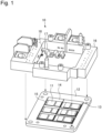
- FIG. 1 is a perspective view illustrating the semiconductor module 10 before assembly according to the comparative example.
- FIG. 2 is a perspective view illustrating the semiconductor module 10 after assembly according to the comparative example.
- FIG. 3 is an explanatory diagram illustrating a connection portion between an electrode pad 15 of a semiconductor chip 11 and a control pin 18 according to the comparative example.
- the semiconductor module 10 according to the comparative example constitutes, for example, a part of a power conversion device that converts DC power supplied from a DC power supply into AC power.
- the semiconductor module 10 according to the comparative example includes the semiconductor chip 11 provided on an insulating substrate 13 fixed to a base plate 12 via a copper pattern 14, and a case 16.
- each of the semiconductor chips 11 is, for example, an insulated gate bipolar transistor (IGBT).
- IGBT insulated gate bipolar transistor
- Six of the semiconductor chips 11 form a bridge circuit that converts DC power into AC power.
- the semiconductor chip 11 includes, for example, the electrode pad 15 connected to a gate of an IGBT. A control signal for turning on or off an IGBT is input to the electrode pad 15 from an external control device.
- the case 16 is a frame body made from resin and having a frame shape in which an opening is provided so as to surround a region where the insulating substrate 13 is arranged in the base plate 12.
- the case 16 includes a bus bar 17 extending in a direction parallel to a plane direction of the base plate 12 from an inner peripheral surface of the opening toward the inside of the opening, and a control pin 18.
- the bus bar 17 is a terminal for inputting power from an external DC power supply to an IGBT.
- the control pin 18 is a terminal for inputting a control signal from an external control device to the electrode pad 15.
- the case 16 is assembled on the base plate 12 on which the semiconductor chip 11 is arranged, so that a connection pad for power supply provided on an upper surface of the semiconductor chip 11 and the bus bar 17 are electrically connected.
- the bus bar 17 and the connection pad for power supply on the semiconductor chip 11 are connected by, for example, solder.
- control pin 18 and the electrode pad 15 for a control signal are wire-bonded by a wire connection device 100, for example.
- the control pin 18 and the electrode pad 15 are electrically connected by a bonding wire 19.
- the electrode pad 15 for a control signal and a part of the bus bar 17 may overlap in plan view.
- the wire connection device 100 interferes with the bus bar 17 only by movement in a horizontal direction and a vertical direction, and the electrode pad 15 for a control signal and the control pin 18 cannot be connected. For this reason, for example, the wire connection device 100 requires complicated control such as setting a moving direction to an oblique direction.
- a semiconductor module according to a first embodiment has a configuration capable of simplifying a process of connecting the semiconductor chip 11 and the control pin 18.
- FIG. 4 is a perspective view illustrating the semiconductor module 1 according to the first embodiment.
- FIG. 5 is an explanatory view illustrating a connection portion between the electrode pad 15 of the semiconductor chip 11 and an electrode pattern 2 according to the first embodiment.
- FIG. 6 is a schematic plan view of the semiconductor module 1 according to the first embodiment. Note that in FIGS. 4 and 6 , illustration of the case 16 is omitted in order to clearly illustrate a characteristic configuration of the semiconductor module 1.
- the semiconductor module 1 includes the semiconductor chip 11 provided on the insulating substrate 13 fixed to the base plate 12 via the copper pattern 14, similarly to the semiconductor module 10 according to the comparative example.
- the semiconductor module 1 includes the electrode pattern 2 provided on a peripheral edge portion on the insulating substrate 13 and connected to the electrode pad 15 of the semiconductor chip 11, and connected to the control pin 18 extending from the case 16 as the case 16 is assembled to the base plate 12.
- the electrode pad 15 is provided on a main surface on the opposite side to a main surface facing the insulating substrate 13 of the semiconductor chip 11.
- the electrode pattern 2 is provided at a position abutting on the control pin 18 when the case 16 is assembled to the base plate 12 in a peripheral edge portion on the insulating substrate 13.
- the electrode pattern 2 is electrically connected to the electrode pad 15 for a control signal in the semiconductor chip 11 by the bonding wire 19 before the case 16 is assembled to the base plate 12.
- the electrode pattern 2 and the control pin 18 are electrically connected at the same time in the process of assembling the base plate 12 to the case 16, so that the process of connecting the semiconductor chip 11 and the control pin 18 can be simplified.
- the electrode pattern 2 and the control pin 18 may be connected by solder, but are preferably connected by ultrasonic bonding.
- the semiconductor module 1 in a case where the electrode pad 15 for a control signal in the semiconductor chip 11 and a part of the bus bar 17 overlap in plan view, the semiconductor chip 11 and the control pin 18 can be connected without performing a complicated connection process.
- the electrode pattern 2 and the copper pattern 14 are formed in a peripheral edge portion on the insulating substrate 13.
- the semiconductor chip 11 is assembled on the insulating substrate 13 via the copper pattern 14. After that, the electrode pad 15 of the semiconductor chip 11 and the electrode pattern 2 are connected by, for example, the bonding wire 19.
- the control pin 18 extending from the case 16 and the electrode pattern 2 are caused to abut on each other. After that, the control pin 18 and the electrode pattern 2 are electrically connected by ultrasonic bonding to complete the semiconductor module 1.
- FIG. 7 is a schematic side view illustrating a positional relationship between the bus bar 17 and the bonding wire 19 according to the first embodiment.
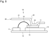
- FIG. 8 is a schematic side view illustrating a positional relationship between a bus bar 20 and the bonding wire 19 according to the variation of the first embodiment.
- a highest position of the bonding wire 19 may become higher than a height position of the bus bar 17 due to control accuracy of the wire connection device 100, and the bonding wire 19 and the bus bar 17 may interfere with each other.
- the semiconductor module 1A according to the variation of the first embodiment includes the case 16 including the bus bar 20 having a shape different from that of the semiconductor module 1 according to the first embodiment. Note that a shape of the case 16 and a position of the control pin 18 are the same as those of the case according to the first embodiment.
- the bus bar 20 includes a first portion 21, a second portion 22, and a third portion 23.
- the first portion 21 overlaps the control pin 18 in plan view, and extends from a position higher than a height position of the control pin 18 in the case 16 to a position beyond the electrode pad 15 in a direction parallel to an extending direction of the control pin 18.
- the second portion 22 extends downward from a tip of the first portion 21.
- the third portion 23 extends in a direction parallel to an extending direction of the first portion 21 from a tip of the second portion 22 and is connected to the semiconductor chip 11.
- the first portion 21 is configured to have a height position higher than a highest position of the bonding wire 19.
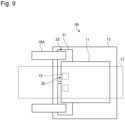
- FIG. 9 is a schematic plan view of the semiconductor module 1B according to the second embodiment.
- the electrode pattern 2 connected to the electrode pad 15 by the bonding wire 19 is provided at a position between the electrode pad 15 of the semiconductor chip 11 in the insulating substrate 13 and the control pin 18.
- a connection process between the semiconductor chip 11 and the control pin 18 can be simplified, but a space for providing the electrode pattern 2 on the insulating substrate 13 at an interval from the electrode pad 15 is required.
- the electrode pad 15 is provided on a main surface facing the insulating substrate 13 of the semiconductor chip 11.
- the semiconductor chip 11 illustrated in FIG. 6 is arranged on the insulating substrate 13 in a state of being reversed.
- an electrode pattern 31 is arranged between the insulating substrate 13 and the electrode pad 15 in the semiconductor chip 11 such that a longitudinal direction intersects an extending direction of a control pin 18A.
- a pair of the control pins 18A are arranged at longer intervals than one side of the semiconductor chip 11. Then, the electrode pattern 31 is connected to the electrode pad 15 at one end portion 32 in a longitudinal direction and connected to the control pin 18A at another end portion 33.
- the electrode pattern 31, the electrode pad 15, and the control pin 18A may be connected by solder, but are preferably connected by ultrasonic bonding.
- a space for providing the electrode pattern 2 at an interval from the electrode pad 15 is not necessary on the insulating substrate 13, and thus, it is not necessary to increase size of the insulating substrate 13, and cost can be reduced.
- the electrode pattern 31 is arranged such that a longitudinal direction intersects an extending direction of the control pin 18A, but may be arranged such that the longitudinal direction is parallel to the extending direction of the control pin 18A.
- control pins 18A are arranged at the same interval as an interval between a pair of the electrode pads 15.
- the electrode pattern 31 is provided on the insulating substrate 13 so as to overlap a curve connecting the control pin 18A and the electrode pad 15 in plan view. Then, the electrode pattern 31 is connected to a lower surface of the electrode pad 15 on an upper surface of the one end portion 32 in the longitudinal direction, and is connected to a lower surface of the control pin 18A on an upper surface of the another end portion 33.
- a space for providing the electrode pattern 2 at an interval from the electrode pad 15 is unnecessary on the insulating substrate 13, and the electrode pad 15 and the control pin 18A are connected by the electrode pattern 31 instead of the bonding wire 19.
Landscapes
- Wire Bonding (AREA)
Abstract
Description
- The present disclosure relates to a semiconductor module, a power conversion device, and a method of manufacturing a semiconductor module.
-
Patent Literature 1 discloses a semiconductor module in which a semiconductor chip assembled in a case and a control pin extending from the case are connected by the same line such as an aluminum wire. - Patent Literature 1:
WO 2018/087890 A - The above-described conventional technique has room for further improvement in terms of simplifying a process of connecting the semiconductor chip and the control pin.
- The present disclosure provides a technique capable of simplifying a process of connecting a semiconductor chip and a control pin.
- A semiconductor module according to one aspect of the present disclosure includes a semiconductor chip and an electrode pattern. The semiconductor chip is provided on an insulating substrate fixed to a base plate. The electrode pattern is provided on a peripheral edge portion on the insulating substrate and connected to an electrode pad of the semiconductor chip, and is connected to a control pin extending from a case as the case is assembled to the base plate.
- According to the present disclosure, a process of connecting a semiconductor chip and a control pin can be simplified.
-
-
FIG. 1 is a perspective view illustrating a semiconductor module before assembly according to a comparative example. -
FIG. 2 is a perspective view illustrating the semiconductor module after assembly according to the comparative example. -
FIG. 3 is an explanatory diagram illustrating a connection portion between an electrode pad of a semiconductor chip and a control pin according to the comparative example. -
FIG. 4 is a perspective view illustrating a semiconductor module according to a first embodiment. -
FIG. 5 is an explanatory view illustrating a connection portion between an electrode pad of a semiconductor chip and an electrode pattern according to the first embodiment. -
FIG. 6 is a schematic plan view of the semiconductor module according to the first embodiment. -
FIG. 7 is a schematic side view illustrating a positional relationship between a bus bar and a bonding wire according to the first embodiment. -
FIG. 8 is a schematic side view illustrating a positional relationship between the bus bar and the bonding wire according to a variation of the first embodiment. -
FIG. 9 is a schematic plan view of the semiconductor module according to a second embodiment. - Hereinafter, a mode (hereinafter, described as an "embodiment") for carrying out a semiconductor module, a power conversion device, and a method of manufacturing a semiconductor module according to the present disclosure will be described in detail with reference to the drawings. Note that the present disclosure is not limited by this embodiment. Further, each embodiment can be appropriately combined within a range in which there is no contradiction in processing content. Further, in each embodiment below, the same reference numerals are given to constituent elements having the same function, and redundant description will be omitted.
- Further, in an embodiment described below, there is a case where expressions such as "constant", "orthogonal", "vertical", and "parallel" is used, but these expressions do not need to strictly mean "constant", "orthogonal", "vertical", and "parallel". That is, each of the expressions described above is assumed to allow deviation in manufacturing accuracy, installation accuracy, and the like, for example.
- First, a
semiconductor module 10 according to a comparative example of the present disclosure will be described with reference toFIGS. 1 to 3 .FIG. 1 is a perspective view illustrating thesemiconductor module 10 before assembly according to the comparative example.FIG. 2 is a perspective view illustrating thesemiconductor module 10 after assembly according to the comparative example.FIG. 3 is an explanatory diagram illustrating a connection portion between anelectrode pad 15 of asemiconductor chip 11 and acontrol pin 18 according to the comparative example. - The
semiconductor module 10 according to the comparative example constitutes, for example, a part of a power conversion device that converts DC power supplied from a DC power supply into AC power. As illustrated inFIG. 1 , thesemiconductor module 10 according to the comparative example includes thesemiconductor chip 11 provided on aninsulating substrate 13 fixed to abase plate 12 via acopper pattern 14, and acase 16. - Here, six of the
semiconductor chips 11 are arranged on theinsulating substrate 13. Each of thesemiconductor chips 11 is, for example, an insulated gate bipolar transistor (IGBT). Six of thesemiconductor chips 11 form a bridge circuit that converts DC power into AC power. Thesemiconductor chip 11 includes, for example, theelectrode pad 15 connected to a gate of an IGBT. A control signal for turning on or off an IGBT is input to theelectrode pad 15 from an external control device. - The
case 16 is a frame body made from resin and having a frame shape in which an opening is provided so as to surround a region where theinsulating substrate 13 is arranged in thebase plate 12. Thecase 16 includes abus bar 17 extending in a direction parallel to a plane direction of thebase plate 12 from an inner peripheral surface of the opening toward the inside of the opening, and acontrol pin 18. - The
bus bar 17 is a terminal for inputting power from an external DC power supply to an IGBT. Thecontrol pin 18 is a terminal for inputting a control signal from an external control device to theelectrode pad 15. - As illustrated in
FIG. 2 , in thesemiconductor module 10, thecase 16 is assembled on thebase plate 12 on which thesemiconductor chip 11 is arranged, so that a connection pad for power supply provided on an upper surface of thesemiconductor chip 11 and thebus bar 17 are electrically connected. Thebus bar 17 and the connection pad for power supply on thesemiconductor chip 11 are connected by, for example, solder. - After the above, as illustrated in
FIG. 3 , thecontrol pin 18 and theelectrode pad 15 for a control signal are wire-bonded by awire connection device 100, for example. By the above, thecontrol pin 18 and theelectrode pad 15 are electrically connected by abonding wire 19. - At this time, in the
semiconductor module 10, theelectrode pad 15 for a control signal and a part of thebus bar 17 may overlap in plan view. In this case, thewire connection device 100 interferes with thebus bar 17 only by movement in a horizontal direction and a vertical direction, and theelectrode pad 15 for a control signal and thecontrol pin 18 cannot be connected. For this reason, for example, thewire connection device 100 requires complicated control such as setting a moving direction to an oblique direction. - On the other hand, for example, in a case where the
electrode pad 15 for a control signal and thecontrol pin 18 are connected before thecase 16 is fixed to thebase plate 12, it is necessary to connect thecase 16 in a state of being slightly shifted in the horizontal direction with respect to thebase plate 12. - In this case, in a process of fixing the
case 16 to thebase plate 12, it is necessary to horizontally move thecase 16 to a fixing position, and thebonding wire 19 may be disconnected by this movement. As described above, in thesemiconductor module 10 according to the comparative example, the process of connecting thesemiconductor chip 11 and thecontrol pin 18 is complicated. In view of the above, a semiconductor module according to a first embodiment has a configuration capable of simplifying a process of connecting thesemiconductor chip 11 and thecontrol pin 18. - Next, a
semiconductor module 1 according to the first embodiment will be described with reference toFIGS. 4 to 6 .FIG. 4 is a perspective view illustrating thesemiconductor module 1 according to the first embodiment.FIG. 5 is an explanatory view illustrating a connection portion between theelectrode pad 15 of thesemiconductor chip 11 and anelectrode pattern 2 according to the first embodiment.FIG. 6 is a schematic plan view of thesemiconductor module 1 according to the first embodiment. Note that inFIGS. 4 and6 , illustration of thecase 16 is omitted in order to clearly illustrate a characteristic configuration of thesemiconductor module 1. - As illustrated in
FIG. 4 , thesemiconductor module 1 includes thesemiconductor chip 11 provided on the insulatingsubstrate 13 fixed to thebase plate 12 via thecopper pattern 14, similarly to thesemiconductor module 10 according to the comparative example. - Furthermore, the
semiconductor module 1 includes theelectrode pattern 2 provided on a peripheral edge portion on the insulatingsubstrate 13 and connected to theelectrode pad 15 of thesemiconductor chip 11, and connected to thecontrol pin 18 extending from thecase 16 as thecase 16 is assembled to thebase plate 12. - Specifically, the
electrode pad 15 is provided on a main surface on the opposite side to a main surface facing the insulatingsubstrate 13 of thesemiconductor chip 11. On the other hand, theelectrode pattern 2 is provided at a position abutting on thecontrol pin 18 when thecase 16 is assembled to thebase plate 12 in a peripheral edge portion on the insulatingsubstrate 13. - Then, as illustrated in
FIG. 5 , theelectrode pattern 2 is electrically connected to theelectrode pad 15 for a control signal in thesemiconductor chip 11 by thebonding wire 19 before thecase 16 is assembled to thebase plate 12. - By the above, in the
semiconductor module 1, theelectrode pattern 2 and thecontrol pin 18 are electrically connected at the same time in the process of assembling thebase plate 12 to thecase 16, so that the process of connecting thesemiconductor chip 11 and thecontrol pin 18 can be simplified. Theelectrode pattern 2 and thecontrol pin 18 may be connected by solder, but are preferably connected by ultrasonic bonding. - Further, as illustrated in
FIG. 6 , in thesemiconductor module 1, in a case where theelectrode pad 15 for a control signal in thesemiconductor chip 11 and a part of thebus bar 17 overlap in plan view, thesemiconductor chip 11 and thecontrol pin 18 can be connected without performing a complicated connection process. - Further, in the
semiconductor module 1, in the process of assembling thebase plate 12 to thecase 16, a positional relationship between theelectrode pattern 2 connected by thebonding wire 19 and theelectrode pad 15 does not change, so that disconnection of thebonding wire 19 can be prevented. - Next, a method for manufacturing the
semiconductor module 1 will be described. In a case of manufacturing thesemiconductor module 1, first, theelectrode pattern 2 and thecopper pattern 14 are formed in a peripheral edge portion on the insulatingsubstrate 13. - Subsequently, the
semiconductor chip 11 is assembled on the insulatingsubstrate 13 via thecopper pattern 14. After that, theelectrode pad 15 of thesemiconductor chip 11 and theelectrode pattern 2 are connected by, for example, thebonding wire 19. - Then, by assembling the
case 16 to thebase plate 12 to which the insulatingsubstrate 13 is fixed, thecontrol pin 18 extending from thecase 16 and theelectrode pattern 2 are caused to abut on each other. After that, thecontrol pin 18 and theelectrode pattern 2 are electrically connected by ultrasonic bonding to complete thesemiconductor module 1. - Next, a semiconductor module 1A according to a variation of the first embodiment will be described with reference to
FIGS. 7 and8 .FIG. 7 is a schematic side view illustrating a positional relationship between thebus bar 17 and thebonding wire 19 according to the first embodiment.FIG. 8 is a schematic side view illustrating a positional relationship between abus bar 20 and thebonding wire 19 according to the variation of the first embodiment. - As illustrated in
FIG. 7 , in thesemiconductor module 1 according to the first embodiment, for example, a highest position of thebonding wire 19 may become higher than a height position of thebus bar 17 due to control accuracy of thewire connection device 100, and thebonding wire 19 and thebus bar 17 may interfere with each other. - In view of the above, as illustrated in
FIG. 8 , the semiconductor module 1A according to the variation of the first embodiment includes thecase 16 including thebus bar 20 having a shape different from that of thesemiconductor module 1 according to the first embodiment. Note that a shape of thecase 16 and a position of thecontrol pin 18 are the same as those of the case according to the first embodiment. - Specifically, the
bus bar 20 according to the variation of the first embodiment includes afirst portion 21, asecond portion 22, and athird portion 23. Thefirst portion 21 overlaps thecontrol pin 18 in plan view, and extends from a position higher than a height position of thecontrol pin 18 in thecase 16 to a position beyond theelectrode pad 15 in a direction parallel to an extending direction of thecontrol pin 18. - The
second portion 22 extends downward from a tip of thefirst portion 21. Thethird portion 23 extends in a direction parallel to an extending direction of thefirst portion 21 from a tip of thesecond portion 22 and is connected to thesemiconductor chip 11. Then, thefirst portion 21 is configured to have a height position higher than a highest position of thebonding wire 19. By the above, thebus bar 20 according to the variation can be prevented from interfering with thebonding wire 19. - Next, a
semiconductor module 1B according to a second embodiment will be described with reference toFIG. 9. FIG. 9 is a schematic plan view of thesemiconductor module 1B according to the second embodiment. - In the
semiconductor module 1 according to the first embodiment, as illustrated inFIG. 6 , theelectrode pattern 2 connected to theelectrode pad 15 by thebonding wire 19 is provided at a position between theelectrode pad 15 of thesemiconductor chip 11 in the insulatingsubstrate 13 and thecontrol pin 18. - By the above, in the
semiconductor module 1 according to the first embodiment, as described above, a connection process between thesemiconductor chip 11 and thecontrol pin 18 can be simplified, but a space for providing theelectrode pattern 2 on the insulatingsubstrate 13 at an interval from theelectrode pad 15 is required. By the above, it is necessary to increase size of the insulatingsubstrate 13. - In view of the above, as illustrated in
FIG. 9 , in thesemiconductor module 1B according to the second embodiment, theelectrode pad 15 is provided on a main surface facing the insulatingsubstrate 13 of thesemiconductor chip 11. Specifically, in thesemiconductor module 1B, thesemiconductor chip 11 illustrated inFIG. 6 is arranged on the insulatingsubstrate 13 in a state of being reversed. - Further, in the
semiconductor module 1B, anelectrode pattern 31 is arranged between the insulatingsubstrate 13 and theelectrode pad 15 in thesemiconductor chip 11 such that a longitudinal direction intersects an extending direction of acontrol pin 18A. - Further, a pair of the control pins 18A are arranged at longer intervals than one side of the
semiconductor chip 11. Then, theelectrode pattern 31 is connected to theelectrode pad 15 at oneend portion 32 in a longitudinal direction and connected to thecontrol pin 18A at anotherend portion 33. Theelectrode pattern 31, theelectrode pad 15, and thecontrol pin 18A may be connected by solder, but are preferably connected by ultrasonic bonding. - By the above, in the
semiconductor module 1B, a space for providing theelectrode pattern 2 at an interval from theelectrode pad 15 is not necessary on the insulatingsubstrate 13, and thus, it is not necessary to increase size of the insulatingsubstrate 13, and cost can be reduced. - Further, in the
semiconductor module 1B, since theelectrode pad 15 and thecontrol pin 18A are connected not by thebonding wire 19 but by theelectrode pattern 31, risk of occurrence of disconnection can be reduced as compared with the connection by thebonding wire 19. - Note that, in the example illustrated in
FIG. 9 , theelectrode pattern 31 is arranged such that a longitudinal direction intersects an extending direction of thecontrol pin 18A, but may be arranged such that the longitudinal direction is parallel to the extending direction of thecontrol pin 18A. - In this case, the control pins 18A are arranged at the same interval as an interval between a pair of the
electrode pads 15. Theelectrode pattern 31 is provided on the insulatingsubstrate 13 so as to overlap a curve connecting thecontrol pin 18A and theelectrode pad 15 in plan view. Then, theelectrode pattern 31 is connected to a lower surface of theelectrode pad 15 on an upper surface of the oneend portion 32 in the longitudinal direction, and is connected to a lower surface of thecontrol pin 18A on an upper surface of the anotherend portion 33. - Also in this case, a space for providing the
electrode pattern 2 at an interval from theelectrode pad 15 is unnecessary on the insulatingsubstrate 13, and theelectrode pad 15 and thecontrol pin 18A are connected by theelectrode pattern 31 instead of thebonding wire 19. By the above, similarly to thesemiconductor module 1B illustrated inFIG. 9 , it is possible to reduce cost and risk of occurrence of disconnection. -
- 1, 1A, 1B, 10 semiconductor module
- 11 semiconductor chip
- 2, 31 electrode pattern
- 12 base plate
- 13 insulating substrate
- 14 copper pattern
- 15 electrode pad
- 16 case
- 17, 20 bus bar
- 18, 18A control pin
- 19 bonding wire
- 21 first portion
- 22 second portion
- 23 third portion
- 32 one end portion
- 33 another end portion
- 100 wire connection device
Claims (7)
- A semiconductor module comprising:a semiconductor chip provided on an insulating substrate fixed to a base plate; andan electrode pattern provided on a peripheral edge portion on the insulating substrate, connected to an electrode pad of the semiconductor chip, and connected to a control pin extending from a case as the case is assembled to the base plate.
- The semiconductor module according to claim 1, wherein
the electrode pad is provided on a main surface on an opposite side to a main surface facing the insulating substrate in the semiconductor chip, and is connected to the electrode pattern by a bonding wire. - The semiconductor module according to claim 2, further comprising a case, whereinthe case includes a bus bar connected to the semiconductor chip by being assembled to the base plate,the bus bar includes:a first portion overlapping the control pin in plan view and extending from a position higher than a height position of the control pin in the case to a position beyond the electrode pad in a direction parallel to an extending direction of the control pin;a second portion extending downward from a tip of the first portion; anda third portion extending in a direction parallel to an extending direction of the first portion from a tip of the second portion and connected to the semiconductor chip, andthe first portion has a height position higher than a highest position of the bonding wire.
- The semiconductor module according to claim 1, whereinthe electrode pad is provided on a main surface facing the insulating substrate in the semiconductor chip, andthe electrode pattern is connected to the electrode pad in one end portion in a longitudinal direction and connected to the control pin in another end portion.
- The semiconductor module according to claim 4, wherein
the electrode pattern is arranged such that the longitudinal direction intersects an extending direction of the control pin. - A power conversion device comprising the semiconductor module according to any one of claims 1 to 5.
- A method of manufacturing a semiconductor module, the method comprising:forming an electrode pattern on a peripheral edge portion on an insulating substrate;assembling a semiconductor chip on the insulating substrate;connecting an electrode pad of the semiconductor chip and the electrode pattern; andconnecting a control pin extending from a case and the electrode pattern by assembling the case to a base plate to which the insulating substrate is fixed.
Applications Claiming Priority (2)
| Application Number | Priority Date | Filing Date | Title |
|---|---|---|---|
| JP2022038337 | 2022-03-11 | ||
| PCT/JP2023/009165 WO2023171767A1 (en) | 2022-03-11 | 2023-03-09 | Semiconductor module, power conversion device, and method for manufacturing semiconductor module |
Publications (2)
| Publication Number | Publication Date |
|---|---|
| EP4492460A1 true EP4492460A1 (en) | 2025-01-15 |
| EP4492460A4 EP4492460A4 (en) | 2026-04-01 |
Family
ID=87935288
Family Applications (1)
| Application Number | Title | Priority Date | Filing Date |
|---|---|---|---|
| EP23766943.7A Pending EP4492460A4 (en) | 2022-03-11 | 2023-03-09 | Semiconductor module, power conversion device and method for manufacturing the semiconductor module |
Country Status (4)
| Country | Link |
|---|---|
| EP (1) | EP4492460A4 (en) |
| JP (1) | JPWO2023171767A1 (en) |
| CN (1) | CN118872053A (en) |
| WO (1) | WO2023171767A1 (en) |
Family Cites Families (6)
| Publication number | Priority date | Publication date | Assignee | Title |
|---|---|---|---|---|
| JP5390064B2 (en) * | 2006-08-30 | 2014-01-15 | ルネサスエレクトロニクス株式会社 | Semiconductor device |
| JP5292779B2 (en) * | 2007-11-26 | 2013-09-18 | 富士電機株式会社 | Semiconductor device |
| WO2015045648A1 (en) * | 2013-09-30 | 2015-04-02 | 富士電機株式会社 | Semiconductor device, method for assembling semiconductor device, component for semiconductor devices and unit module |
| JP6401444B2 (en) * | 2013-10-07 | 2018-10-10 | ローム株式会社 | Power module and manufacturing method thereof |
| JP6725004B2 (en) | 2016-11-11 | 2020-07-15 | 三菱電機株式会社 | Semiconductor device, inverter unit and automobile |
| CN115023791B (en) * | 2020-01-28 | 2025-08-26 | 力特保险丝公司 | Semiconductor chip package and assembly method |
-
2023
- 2023-03-09 EP EP23766943.7A patent/EP4492460A4/en active Pending
- 2023-03-09 JP JP2024506409A patent/JPWO2023171767A1/ja active Pending
- 2023-03-09 CN CN202380026267.5A patent/CN118872053A/en active Pending
- 2023-03-09 WO PCT/JP2023/009165 patent/WO2023171767A1/en not_active Ceased
Also Published As
| Publication number | Publication date |
|---|---|
| JPWO2023171767A1 (en) | 2023-09-14 |
| EP4492460A4 (en) | 2026-04-01 |
| CN118872053A (en) | 2024-10-29 |
| WO2023171767A1 (en) | 2023-09-14 |
Similar Documents
| Publication | Publication Date | Title |
|---|---|---|
| US10978379B2 (en) | Semiconductor device with island and associated leads | |
| TWI470709B (en) | Method of mounting a connection board to a semiconductor wafer in a lead frame package | |
| CN205264696U (en) | Semiconductor device | |
| US6710439B2 (en) | Three-dimensional power semiconductor module and method of manufacturing the same | |
| US20110012245A1 (en) | Semiconductor device | |
| CN112913009B (en) | Semiconductor device and lead frame material | |
| CN101887876A (en) | Semiconductor package, lead frame, and wiring board having the package and lead frame | |
| JPH06252328A (en) | Lead frame for mounting semiconductor element | |
| US10699987B2 (en) | SMD package with flat contacts to prevent bottleneck | |
| JPH1131717A (en) | Semiconductor chip and display device equipped with the same | |
| JPH1145903A (en) | Semiconductor element and semiconductor device | |
| KR20050020930A (en) | Circuit device | |
| CN115117038B (en) | semiconductor devices | |
| EP3882960A1 (en) | Semiconductor device and method for manufacturing same | |
| CN1007477B (en) | Integrated circuit device having slanted peripheral circuit | |
| CN118872053A (en) | Semiconductor module, power conversion device, and method for manufacturing semiconductor module | |
| JPH01132142A (en) | Package structure of semiconductor device | |
| US11043435B1 (en) | Semiconductor die with hybrid wire bond pads | |
| CN222483355U (en) | Chip packaging structure and electronic equipment | |
| US6118173A (en) | Lead frame and a semiconductor device | |
| CN222581160U (en) | Chip packaging structure and chip module | |
| US20260068737A1 (en) | Semiconductor module and manufacturing method of semiconductor module | |
| US20240266263A1 (en) | Semiconductor apparatus | |
| KR100235107B1 (en) | Tab package | |
| US20070108570A1 (en) | Semiconductor device and method of manufacturing the same |
Legal Events
| Date | Code | Title | Description |
|---|---|---|---|
| STAA | Information on the status of an ep patent application or granted ep patent |
Free format text: STATUS: THE INTERNATIONAL PUBLICATION HAS BEEN MADE |
|
| PUAI | Public reference made under article 153(3) epc to a published international application that has entered the european phase |
Free format text: ORIGINAL CODE: 0009012 |
|
| STAA | Information on the status of an ep patent application or granted ep patent |
Free format text: STATUS: REQUEST FOR EXAMINATION WAS MADE |
|
| 17P | Request for examination filed |
Effective date: 20241008 |
|
| AK | Designated contracting states |
Kind code of ref document: A1 Designated state(s): AL AT BE BG CH CY CZ DE DK EE ES FI FR GB GR HR HU IE IS IT LI LT LU LV MC ME MK MT NL NO PL PT RO RS SE SI SK SM TR |
|
| DAV | Request for validation of the european patent (deleted) | ||
| DAX | Request for extension of the european patent (deleted) | ||
| REG | Reference to a national code |
Ref country code: DE Ref legal event code: R079 Free format text: PREVIOUS MAIN CLASS: H01L0025070000 Ipc: H10W0072500000 |
|
| A4 | Supplementary search report drawn up and despatched |
Effective date: 20260303 |
|
| RIC1 | Information provided on ipc code assigned before grant |
Ipc: H10W 72/50 20260101AFI20260225BHEP Ipc: H10W 72/60 20260101ALI20260225BHEP Ipc: H10W 72/00 20260101ALI20260225BHEP Ipc: H10W 74/00 20260101ALI20260225BHEP Ipc: H10W 76/15 20260101ALI20260225BHEP Ipc: H10W 76/157 20260101ALI20260225BHEP Ipc: H10W 76/47 20260101ALI20260225BHEP Ipc: H10W 90/00 20260101ALI20260225BHEP Ipc: H10W 70/65 20260101ALI20260225BHEP |