EP4489074A1 - Array substrate and display panel - Google Patents
Array substrate and display panel Download PDFInfo
- Publication number
- EP4489074A1 EP4489074A1 EP23193869.7A EP23193869A EP4489074A1 EP 4489074 A1 EP4489074 A1 EP 4489074A1 EP 23193869 A EP23193869 A EP 23193869A EP 4489074 A1 EP4489074 A1 EP 4489074A1
- Authority
- EP
- European Patent Office
- Prior art keywords
- doped
- layer
- doped portion
- gate
- array substrate
- Prior art date
- Legal status (The legal status is an assumption and is not a legal conclusion. Google has not performed a legal analysis and makes no representation as to the accuracy of the status listed.)
- Pending
Links
- 239000000758 substrate Substances 0.000 title claims abstract description 110
- 150000002500 ions Chemical class 0.000 claims abstract description 36
- 230000000149 penetrating effect Effects 0.000 claims description 8
- 239000010410 layer Substances 0.000 description 255
- 239000004065 semiconductor Substances 0.000 description 51
- 239000010949 copper Substances 0.000 description 26
- 238000004519 manufacturing process Methods 0.000 description 21
- 238000000034 method Methods 0.000 description 21
- 239000010936 titanium Substances 0.000 description 18
- VYPSYNLAJGMNEJ-UHFFFAOYSA-N Silicium dioxide Chemical compound O=[Si]=O VYPSYNLAJGMNEJ-UHFFFAOYSA-N 0.000 description 15
- 229910052814 silicon oxide Inorganic materials 0.000 description 15
- RYGMFSIKBFXOCR-UHFFFAOYSA-N Copper Chemical compound [Cu] RYGMFSIKBFXOCR-UHFFFAOYSA-N 0.000 description 14
- 229910052802 copper Inorganic materials 0.000 description 14
- 239000000463 material Substances 0.000 description 12
- 229910052581 Si3N4 Inorganic materials 0.000 description 11
- HQVNEWCFYHHQES-UHFFFAOYSA-N silicon nitride Chemical compound N12[Si]34N5[Si]62N3[Si]51N64 HQVNEWCFYHHQES-UHFFFAOYSA-N 0.000 description 11
- ZOKXTWBITQBERF-UHFFFAOYSA-N Molybdenum Chemical compound [Mo] ZOKXTWBITQBERF-UHFFFAOYSA-N 0.000 description 10
- RTAQQCXQSZGOHL-UHFFFAOYSA-N Titanium Chemical compound [Ti] RTAQQCXQSZGOHL-UHFFFAOYSA-N 0.000 description 10
- XLOMVQKBTHCTTD-UHFFFAOYSA-N Zinc monoxide Chemical compound [Zn]=O XLOMVQKBTHCTTD-UHFFFAOYSA-N 0.000 description 10
- 229910052750 molybdenum Inorganic materials 0.000 description 10
- 239000011733 molybdenum Substances 0.000 description 10
- 229910052719 titanium Inorganic materials 0.000 description 10
- 229910044991 metal oxide Inorganic materials 0.000 description 8
- 150000004706 metal oxides Chemical class 0.000 description 8
- XAGFODPZIPBFFR-UHFFFAOYSA-N aluminium Chemical compound [Al] XAGFODPZIPBFFR-UHFFFAOYSA-N 0.000 description 7
- 229910016027 MoTi Inorganic materials 0.000 description 6
- 229910001069 Ti alloy Inorganic materials 0.000 description 6
- 229910052782 aluminium Inorganic materials 0.000 description 6
- ZPZCREMGFMRIRR-UHFFFAOYSA-N molybdenum titanium Chemical compound [Ti].[Mo] ZPZCREMGFMRIRR-UHFFFAOYSA-N 0.000 description 6
- TWNQGVIAIRXVLR-UHFFFAOYSA-N oxo(oxoalumanyloxy)alumane Chemical compound O=[Al]O[Al]=O TWNQGVIAIRXVLR-UHFFFAOYSA-N 0.000 description 5
- 229910021420 polycrystalline silicon Inorganic materials 0.000 description 5
- 229920005591 polysilicon Polymers 0.000 description 5
- YVTHLONGBIQYBO-UHFFFAOYSA-N zinc indium(3+) oxygen(2-) Chemical compound [O--].[Zn++].[In+3] YVTHLONGBIQYBO-UHFFFAOYSA-N 0.000 description 5
- 239000011787 zinc oxide Substances 0.000 description 5
- 238000010586 diagram Methods 0.000 description 4
- 229910052738 indium Inorganic materials 0.000 description 4
- APFVFJFRJDLVQX-UHFFFAOYSA-N indium atom Chemical compound [In] APFVFJFRJDLVQX-UHFFFAOYSA-N 0.000 description 4
- -1 phosphorus ions Chemical class 0.000 description 4
- XUIMIQQOPSSXEZ-UHFFFAOYSA-N Silicon Chemical compound [Si] XUIMIQQOPSSXEZ-UHFFFAOYSA-N 0.000 description 3
- 229910021417 amorphous silicon Inorganic materials 0.000 description 3
- 238000000137 annealing Methods 0.000 description 3
- 238000010438 heat treatment Methods 0.000 description 3
- 239000004973 liquid crystal related substance Substances 0.000 description 3
- 229910052710 silicon Inorganic materials 0.000 description 3
- 239000010703 silicon Substances 0.000 description 3
- GYHNNYVSQQEPJS-UHFFFAOYSA-N Gallium Chemical compound [Ga] GYHNNYVSQQEPJS-UHFFFAOYSA-N 0.000 description 2
- 230000015572 biosynthetic process Effects 0.000 description 2
- 229910052796 boron Inorganic materials 0.000 description 2
- 238000002425 crystallisation Methods 0.000 description 2
- 239000002019 doping agent Substances 0.000 description 2
- 229910052733 gallium Inorganic materials 0.000 description 2
- AMGQUBHHOARCQH-UHFFFAOYSA-N indium;oxotin Chemical compound [In].[Sn]=O AMGQUBHHOARCQH-UHFFFAOYSA-N 0.000 description 2
- 238000012986 modification Methods 0.000 description 2
- 230000004048 modification Effects 0.000 description 2
- 229910052698 phosphorus Inorganic materials 0.000 description 2
- 239000011574 phosphorus Substances 0.000 description 2
- ATJFFYVFTNAWJD-UHFFFAOYSA-N Tin Chemical compound [Sn] ATJFFYVFTNAWJD-UHFFFAOYSA-N 0.000 description 1
- HCHKCACWOHOZIP-UHFFFAOYSA-N Zinc Chemical compound [Zn] HCHKCACWOHOZIP-UHFFFAOYSA-N 0.000 description 1
- DZLPZFLXRVRDAE-UHFFFAOYSA-N [O--].[O--].[O--].[O--].[Al+3].[Zn++].[In+3] Chemical compound [O--].[O--].[O--].[O--].[Al+3].[Zn++].[In+3] DZLPZFLXRVRDAE-UHFFFAOYSA-N 0.000 description 1
- VGLYDBMDZXTCJA-UHFFFAOYSA-N aluminum zinc oxygen(2-) tin(4+) Chemical compound [O-2].[Al+3].[Sn+4].[Zn+2] VGLYDBMDZXTCJA-UHFFFAOYSA-N 0.000 description 1
- 230000009286 beneficial effect Effects 0.000 description 1
- 239000000969 carrier Substances 0.000 description 1
- 230000008025 crystallization Effects 0.000 description 1
- AJNVQOSZGJRYEI-UHFFFAOYSA-N digallium;oxygen(2-) Chemical compound [O-2].[O-2].[O-2].[Ga+3].[Ga+3] AJNVQOSZGJRYEI-UHFFFAOYSA-N 0.000 description 1
- 238000005530 etching Methods 0.000 description 1
- 239000010408 film Substances 0.000 description 1
- 229910001195 gallium oxide Inorganic materials 0.000 description 1
- YZZNJYQZJKSEER-UHFFFAOYSA-N gallium tin Chemical compound [Ga].[Sn] YZZNJYQZJKSEER-UHFFFAOYSA-N 0.000 description 1
- 239000011521 glass Substances 0.000 description 1
- 230000020169 heat generation Effects 0.000 description 1
- 239000011229 interlayer Substances 0.000 description 1
- 238000005224 laser annealing Methods 0.000 description 1
- 229920000642 polymer Polymers 0.000 description 1
- 239000002096 quantum dot Substances 0.000 description 1
- 238000006467 substitution reaction Methods 0.000 description 1
- 239000010409 thin film Substances 0.000 description 1
- 229910001887 tin oxide Inorganic materials 0.000 description 1
- WFKWXMTUELFFGS-UHFFFAOYSA-N tungsten Chemical compound [W] WFKWXMTUELFFGS-UHFFFAOYSA-N 0.000 description 1
- 229910052721 tungsten Inorganic materials 0.000 description 1
- 239000010937 tungsten Substances 0.000 description 1
- 229910052725 zinc Inorganic materials 0.000 description 1
- 239000011701 zinc Substances 0.000 description 1
Images



Classifications
-
- H—ELECTRICITY
- H10—SEMICONDUCTOR DEVICES; ELECTRIC SOLID-STATE DEVICES NOT OTHERWISE PROVIDED FOR
- H10D—INORGANIC ELECTRIC SEMICONDUCTOR DEVICES
- H10D86/00—Integrated devices formed in or on insulating or conducting substrates, e.g. formed in silicon-on-insulator [SOI] substrates or on stainless steel or glass substrates
- H10D86/40—Integrated devices formed in or on insulating or conducting substrates, e.g. formed in silicon-on-insulator [SOI] substrates or on stainless steel or glass substrates characterised by multiple TFTs
- H10D86/421—Integrated devices formed in or on insulating or conducting substrates, e.g. formed in silicon-on-insulator [SOI] substrates or on stainless steel or glass substrates characterised by multiple TFTs having a particular composition, shape or crystalline structure of the active layer
-
- H—ELECTRICITY
- H10—SEMICONDUCTOR DEVICES; ELECTRIC SOLID-STATE DEVICES NOT OTHERWISE PROVIDED FOR
- H10D—INORGANIC ELECTRIC SEMICONDUCTOR DEVICES
- H10D86/00—Integrated devices formed in or on insulating or conducting substrates, e.g. formed in silicon-on-insulator [SOI] substrates or on stainless steel or glass substrates
- H10D86/40—Integrated devices formed in or on insulating or conducting substrates, e.g. formed in silicon-on-insulator [SOI] substrates or on stainless steel or glass substrates characterised by multiple TFTs
- H10D86/60—Integrated devices formed in or on insulating or conducting substrates, e.g. formed in silicon-on-insulator [SOI] substrates or on stainless steel or glass substrates characterised by multiple TFTs wherein the TFTs are in active matrices
-
- G—PHYSICS
- G09—EDUCATION; CRYPTOGRAPHY; DISPLAY; ADVERTISING; SEALS
- G09F—DISPLAYING; ADVERTISING; SIGNS; LABELS OR NAME-PLATES; SEALS
- G09F9/00—Indicating arrangements for variable information in which the information is built-up on a support by selection or combination of individual elements
- G09F9/30—Indicating arrangements for variable information in which the information is built-up on a support by selection or combination of individual elements in which the desired character or characters are formed by combining individual elements
- G09F9/33—Indicating arrangements for variable information in which the information is built-up on a support by selection or combination of individual elements in which the desired character or characters are formed by combining individual elements being semiconductor devices, e.g. diodes
-
- G—PHYSICS
- G09—EDUCATION; CRYPTOGRAPHY; DISPLAY; ADVERTISING; SEALS
- G09F—DISPLAYING; ADVERTISING; SIGNS; LABELS OR NAME-PLATES; SEALS
- G09F9/00—Indicating arrangements for variable information in which the information is built-up on a support by selection or combination of individual elements
- G09F9/30—Indicating arrangements for variable information in which the information is built-up on a support by selection or combination of individual elements in which the desired character or characters are formed by combining individual elements
- G09F9/33—Indicating arrangements for variable information in which the information is built-up on a support by selection or combination of individual elements in which the desired character or characters are formed by combining individual elements being semiconductor devices, e.g. diodes
- G09F9/335—Indicating arrangements for variable information in which the information is built-up on a support by selection or combination of individual elements in which the desired character or characters are formed by combining individual elements being semiconductor devices, e.g. diodes being organic light emitting diodes [OLED]
-
- H—ELECTRICITY
- H10—SEMICONDUCTOR DEVICES; ELECTRIC SOLID-STATE DEVICES NOT OTHERWISE PROVIDED FOR
- H10D—INORGANIC ELECTRIC SEMICONDUCTOR DEVICES
- H10D30/00—Field-effect transistors [FET]
- H10D30/60—Insulated-gate field-effect transistors [IGFET]
- H10D30/67—Thin-film transistors [TFT]
- H10D30/6704—Thin-film transistors [TFT] having supplementary regions or layers in the thin films or in the insulated bulk substrates for controlling properties of the device
- H10D30/6713—Thin-film transistors [TFT] having supplementary regions or layers in the thin films or in the insulated bulk substrates for controlling properties of the device characterised by the properties of the source or drain regions, e.g. compositions or sectional shapes
- H10D30/6715—Thin-film transistors [TFT] having supplementary regions or layers in the thin films or in the insulated bulk substrates for controlling properties of the device characterised by the properties of the source or drain regions, e.g. compositions or sectional shapes characterised by the doping profiles, e.g. having lightly-doped source or drain extensions
- H10D30/6717—Thin-film transistors [TFT] having supplementary regions or layers in the thin films or in the insulated bulk substrates for controlling properties of the device characterised by the properties of the source or drain regions, e.g. compositions or sectional shapes characterised by the doping profiles, e.g. having lightly-doped source or drain extensions the source and the drain regions being asymmetrical
-
- H—ELECTRICITY
- H10—SEMICONDUCTOR DEVICES; ELECTRIC SOLID-STATE DEVICES NOT OTHERWISE PROVIDED FOR
- H10D—INORGANIC ELECTRIC SEMICONDUCTOR DEVICES
- H10D62/00—Semiconductor bodies, or regions thereof, of devices having potential barriers
- H10D62/10—Shapes, relative sizes or dispositions of the regions of the semiconductor bodies; Shapes of the semiconductor bodies
- H10D62/124—Shapes, relative sizes or dispositions of the regions of semiconductor bodies or of junctions between the regions
-
- H—ELECTRICITY
- H10—SEMICONDUCTOR DEVICES; ELECTRIC SOLID-STATE DEVICES NOT OTHERWISE PROVIDED FOR
- H10D—INORGANIC ELECTRIC SEMICONDUCTOR DEVICES
- H10D86/00—Integrated devices formed in or on insulating or conducting substrates, e.g. formed in silicon-on-insulator [SOI] substrates or on stainless steel or glass substrates
- H10D86/01—Manufacture or treatment
- H10D86/021—Manufacture or treatment of multiple TFTs
- H10D86/0221—Manufacture or treatment of multiple TFTs comprising manufacture, treatment or patterning of TFT semiconductor bodies
-
- H—ELECTRICITY
- H10—SEMICONDUCTOR DEVICES; ELECTRIC SOLID-STATE DEVICES NOT OTHERWISE PROVIDED FOR
- H10D—INORGANIC ELECTRIC SEMICONDUCTOR DEVICES
- H10D86/00—Integrated devices formed in or on insulating or conducting substrates, e.g. formed in silicon-on-insulator [SOI] substrates or on stainless steel or glass substrates
- H10D86/40—Integrated devices formed in or on insulating or conducting substrates, e.g. formed in silicon-on-insulator [SOI] substrates or on stainless steel or glass substrates characterised by multiple TFTs
- H10D86/421—Integrated devices formed in or on insulating or conducting substrates, e.g. formed in silicon-on-insulator [SOI] substrates or on stainless steel or glass substrates characterised by multiple TFTs having a particular composition, shape or crystalline structure of the active layer
- H10D86/427—Integrated devices formed in or on insulating or conducting substrates, e.g. formed in silicon-on-insulator [SOI] substrates or on stainless steel or glass substrates characterised by multiple TFTs having a particular composition, shape or crystalline structure of the active layer having different thicknesses of the semiconductor bodies in different TFTs
-
- H—ELECTRICITY
- H10—SEMICONDUCTOR DEVICES; ELECTRIC SOLID-STATE DEVICES NOT OTHERWISE PROVIDED FOR
- H10D—INORGANIC ELECTRIC SEMICONDUCTOR DEVICES
- H10D86/00—Integrated devices formed in or on insulating or conducting substrates, e.g. formed in silicon-on-insulator [SOI] substrates or on stainless steel or glass substrates
- H10D86/40—Integrated devices formed in or on insulating or conducting substrates, e.g. formed in silicon-on-insulator [SOI] substrates or on stainless steel or glass substrates characterised by multiple TFTs
- H10D86/431—Integrated devices formed in or on insulating or conducting substrates, e.g. formed in silicon-on-insulator [SOI] substrates or on stainless steel or glass substrates characterised by multiple TFTs having different compositions, shapes, layouts or thicknesses of gate insulators in different TFTs
-
- H—ELECTRICITY
- H10—SEMICONDUCTOR DEVICES; ELECTRIC SOLID-STATE DEVICES NOT OTHERWISE PROVIDED FOR
- H10D—INORGANIC ELECTRIC SEMICONDUCTOR DEVICES
- H10D86/00—Integrated devices formed in or on insulating or conducting substrates, e.g. formed in silicon-on-insulator [SOI] substrates or on stainless steel or glass substrates
- H10D86/40—Integrated devices formed in or on insulating or conducting substrates, e.g. formed in silicon-on-insulator [SOI] substrates or on stainless steel or glass substrates characterised by multiple TFTs
- H10D86/421—Integrated devices formed in or on insulating or conducting substrates, e.g. formed in silicon-on-insulator [SOI] substrates or on stainless steel or glass substrates characterised by multiple TFTs having a particular composition, shape or crystalline structure of the active layer
- H10D86/423—Integrated devices formed in or on insulating or conducting substrates, e.g. formed in silicon-on-insulator [SOI] substrates or on stainless steel or glass substrates characterised by multiple TFTs having a particular composition, shape or crystalline structure of the active layer comprising semiconductor materials not belonging to the Group IV, e.g. InGaZnO
Definitions
- the present disclosure relates to the field of display, and in particular, to an array substrate and a display panel.
- transistors with high mobility suffer from poor stability in operation.
- An object of the present disclosure is to provide an array substrate and a display panel to improve poor stability of transistors.
- an array substrate including:
- the present disclosure provides a display panel including the above array substrate.
- the doping concentration of ions in the second doped sub-portion is less than the doping concentration of ions in the first doped sub-portion, and the doping concentration of ions in the first doped sub-portion is the same as a doping concentration of ions in the second doped portion, the resistance of the second doped sub-portion is greater than that of the first doped sub-portion, thereby reducing the voltage drop of the first doped portion connected to the drain, and improving the problem of poor stability of the first transistor due to self-heating.
- FIGs. 1A to 1H are schematic structural diagrams of a process for manufacturing an array substrate according to some embodiments of the present disclosure. The process for manufacturing an array substrate according to some embodiments of the present disclosure is described in detail with reference to FIGs. 1A to 1H .
- the process for manufacturing the array substrate before the step of forming a first semiconductor layer 103a on the substrate 101, the process for manufacturing the array substrate further includes forming a buffer layer 102 on the substrate 101.
- the substrate 101 includes a glass substrate, but is not limited thereto.
- the substrate 101 may also be a flexible substrate including a polymer layer.
- the buffer layer 102 includes, but is not limited to, a silicon oxide layer, a silicon nitride layer, a silicon oxynitride layer, or a stacked layer of a silicon nitride layer and a silicon oxide layer.
- the step of forming a first semiconductor layer 103a on the substrate 101 includes forming a first semiconductor layer 103a on a surface of the buffer layer 102 away from the substrate 101.
- the first semiconductor layer 103a is a single semiconductor layer.
- Materials of the first semiconductor layer 103a include amorphous silicon, polysilicon, or metal oxides.
- Polysilicon can be obtained by subjecting amorphous silicon to laser annealing crystallization or other crystallization methods.
- the metal oxide includes at least one of indium element, zinc element, tungsten element, tin element, gallium element, and aluminum element.
- the material of the metal oxide includes, but is not limited to a metal oxide with low leakage current, such as indium gallium zinc oxide (IGZO), indium gallium tin oxide (IGTO), indium gallium oxide (IGO), indium zinc oxide (IZO), aluminum indium zinc oxide (AIZO), aluminum tin zinc oxide (ATZO), or the like.
- the process for manufacturing the array substrate further includes forming a fourth insulating layer 1041 on the first semiconductor layer 103a.
- the fourth insulating layer 1041 overlaps with part of the first semiconductor layer 103a.
- the fourth insulating layer 1041 is a first gate insulating layer.
- the material of the fourth insulating layer 1041 includes, but is not limited to, at least one of silicon oxide, aluminum oxide, and silicon nitride.
- the fourth insulating layer 1041 includes a silicon oxide layer, or a stacked layer of an aluminum oxide layer, a silicon nitride layer and a silicon oxide layer, or a stacked of a silicon oxide layer, a silicon nitride layer and a silicon oxide layer.
- the step of forming a first gate 105 overlapping the first semiconductor layer 103a on one side of the first semiconductor layer 103a away from the substrate 101 includes forming a first gate 105 on one side of the fourth insulating layer 1041 away from the substrate 101.
- the material of the first gate 105 includes, but is not limited to, at least one of molybdenum, aluminum, copper, titanium, indium zinc oxide, and indium tin oxide.
- the first gate 105 includes a molybdenum layer (Mo), or a stacked layer of a molybdenum layer and an aluminum layer (Mo/Al), or a stacked layer of a molybdenum layer and a copper layer (Mo/Cu), or a stacked layer of a molybdenum-titanium alloy layer and a copper layer (MoTi/Cu), or a stacked layer of a molybdenum-titanium alloy layer, a copper layer, and a molybdenum-titanium alloy layer that are sequentially stacked (MoTi/Cu/MoTi), or a stacked layer of a titanium layer, an aluminum layer, and a titanium layer that are sequentially stacked (Ti/Al/T
- first semiconductor layer 103a for the first time by using the first gate 105 as a mask, so that the first semiconductor layer 103a subjected to the first doping process is formed with a first initial doped portion 1032a, a second initial doped portion 1033a and a first channel portion 1031.
- the first initial doped portion 1032a and the second initial doped portion 1033a are connected to opposite ends of the first channel portion 1031, respectively.
- the doped portions of the first semiconductor layer 103a form the first initial doped portion 1032a and the second initial doped portion 1033a, respectively, and the undoped portion of the first semiconductor layer 103a forms the first channel portion 1031.
- a doping concentration of ions in the first initial doped portion 1032a is the same as that in the second initial doped portion 1033a.
- Both the first initial doped portion 1032a and the second initial doped portion 1033a have conductivity.
- An orthographic projection of the first channel portion 1031 on the substrate 101 completely overlaps with an orthographic projection of the first gate 105 on the substrate 101. In other words, the orthographic projection of the first channel portion 1031 on the substrate 101 is basically the same as the the orthographic projection of the first gate 105 on the substrate 101.
- the length of the first initial doped portion 1032a is greater than the length of the second initial doped portion 1033a, and the length of the first initial doped portion 1032a is long enough to facilitate subsequent differential design of the resistances in different regions of the first initial doped portion 1032a.
- a distance between an edge of the first gate 105 close to the first initial doped portion 1032a and an edge of the first initial doped portion 1032a away from the first channel portion 1031 is greater than a distance between an edge of the first gate 105 close to the second initial doped portion 1033a and an edge of the second initial doped portion 1033a away from the first channel portion 1031.
- the length of the first initial doped portion 1032a may also be less than or equal to the length of the second initial doped portion 1033a.
- the first initial doped portion 1032a has a first region 1032a1 and a second region 1032a2.
- the second region 1032a2 is located between the first region 1032a1 and the first channel portion 1031.
- no further process of doping ions is required.
- the first doping is N-type heavy doping or P-type heavy doping.
- N-type heavily doped ions include, but are not limited to, phosphorus ions.
- P-type heavily doped ions include, but are not limited to, boron ions.
- the doping concentration of the first doping ranges from 1 ⁇ 10 14 /cm 2 to 9 ⁇ 10 14 /cm 2 .
- the doping concentration of the first doping is 4 ⁇ 10 14 /cm 2 .
- a second semiconductor layer 106a on one side of the first gate 105 away from the substrate 101.
- the second semiconductor layer 106a overlaps with the first channel portion 1031, the second region 1032a2, part of the first region 1032a1 and the second initial doped portion 1033a.
- the process for manufacturing the array substrate before the step of forming a second semiconductor layer 106a on one side of the first gate 105 away from the substrate 101, the process for manufacturing the array substrate further includes forming a first insulating layer 1042 covering the first gate 105, the first initial doped portion 1032a, the second initial doped portion 1033a and the buffer layer 102, and forming a first via 10a overlapping with the second initial doped portion 1033a in the first insulating layer 1042.
- the material of the first insulating layer 1042 includes, but is not limited to, at least one of silicon oxide, silicon oxynitride, aluminum oxide, and silicon nitride.
- the first insulating layer 1042 includes any one of a silicon oxide layer, a silicon nitride layer, a silicon oxynitride layer, and or a stacked layer of a silicon nitride layer and a silicon oxide layer.
- the step of forming the second semiconductor layer 106a on the side of the first gate 105 away from the substrate 101 includes forming the second semiconductor layer 106a on the surface of the first insulating layer 1042 away from the substrate 101 and in the first via 10a.
- the second semiconductor layer 106a is a single semiconductor layer.
- the material of the second semiconductor layer 106a includes, but is not limited to, amorphous silicon, polysilicon, or metal oxides. The selection of the polysilicon and the metal oxides is as described above, and details are not described herein.
- the material of the second semiconductor layer 106a is the same as, but not limited to, the material of the first semiconductor layer 103a.
- both the second semiconductor layer 106a and the first semiconductor layer 103a are metal oxide semiconductor layers.
- the material of the second semiconductor layer 106a may be different from the material of the first semiconductor layer 103a.
- the first semiconductor layer 103a is a metal oxide semiconductor layer
- the second semiconductor layer 106a is a polysilicon semiconductor layer.
- the process for manufacturing the array substrate before the step of forming the second gate 107 on the side of the second semiconductor layer 106a away from the substrate 101, the process for manufacturing the array substrate further includes a step of forming a second insulating layer 1043 covering the second semiconductor layer 106a and the first insulating layer 1042.
- the second insulating layer 1043 is a second gate insulating layer.
- the material of the second insulating layer 1043 includes, but is not limited to, at least one of silicon oxide, aluminum oxide, and silicon nitride.
- the second insulating layer 1043 includes a silicon oxide layer, or a stacked layer of an aluminum oxide layer, a silicon nitride layer and a silicon oxide layer, or a stacked layer of a silicon oxide layer, a silicon nitride layer and a silicon oxide layer.
- the doped portions in the second semiconductor layer 106a form a third doped portion 1062 and a fourth doped portion 1063, respectively; and the undoped portion in the second semiconductor layer 106a forms a second channel portion 1061.
- the third doped portion 1062, and the fourth doped portion 1063 are connected to opposite sides of the second channel portion 1061, respectively.
- the second channel portion 1061, the third doped portion 1062, and the fourth doped portion 1063 constitute the second active layer 106.
- part of the first initial doped portion 1032a located in the first region 1032a1 that is subjected to the second doping forms the first doped sub-portion 10321.
- the second initial doped portion 1033a that is subjected to the second doping forms the second doped portion 1033.
- part of the first initial doped portion 1032a located in the second region 1032a2 that is not subjected to the second doping forms the second doped sub-portion 10322.
- the first doped sub-portion 10321 and the second doped sub-portion 10322 constitute the first doped portion 1032.
- the first doped portion 1032, the second doped portion 1033 and the first channel portion 1031 constitute the first active layer 103.
- an orthographic projection of the second channel portion 1061 on the substrate 101 completely overlaps with an orthographic projection of the second gate 107 on the substrate 101.
- the orthographic projection of the second channel portion 1061 on the substrate 101 is basically the same as the orthographic projection of the second gate 107 on the substrate 101.
- the second channel portion 1061 overlaps with the first channel portion 1031 and the second doped sub-portion 10322; and the third doped portion 1062 overlaps with the second doped portion 1033; so that the second channel portion 1061 overlaps with the first channel portion 1031, and the length of the second channel portion 1061 is greater than that of the first channel portion 1031, thereby facilitating the formation of the second active layer 106 and the first active layer 103 simultaneously by using a self-alignment process in combination with a process of doping ions by using the second gate 107 as a mask, thus further reducing the number of masks required for manufacturing the array substrate.
- the doping concentration of ions in the third doped portion 1062 is the same as that in the fourth doped portion 1063, and the third doped portion 1062 and the fourth doped portion 1063 have conductivity due to the ions doped therein.
- the third doped portion 1062 is contacted and connected with the second doped portion 1033 through the first via 10a, so that wirings connecting the third doped portion 1062 and the second doped portion 1033 are reduced, and the number of masks required for manufacturing the wirings is further reduced.
- the doping concentration of ions in the first doped sub-portion 10321 is the same as that in the second doped portion 1033, and the doping concentration of ions in the second doped sub-portion 10322 is lower than that in the first doped sub-portion 10321.
- the resistance of the second doped sub-portion 10322 is greater than that of the first doped sub-portion 10321, which reduces the voltage drop of the first doped portion 1032 that needs to be connected to the drain.
- a ratio of the doping concentration of ions in the second doped sub-portion 10322 to the doping concentration of ions in the first doped sub-portion 10321 is greater than or equal to 0.02 and less than or equal to 0.1, which can increase the resistance of the second doped sub-portion 10322 while reduce the resistance of the first doped sub-portion 10321, thus reducing the connection impedance between the first doped sub-portion 10321 and the drain while reducing the voltage drop of the first doped sub-portion 1032 that needs to be connected to the drain.
- both the first doping and the second doping are N-type heavy doping, or both the first doping and the second doping are P-type heavy doping.
- the dopant ions used in first doping are the same as those in the second doping, but is not limited thereto, for example, the dopant ions used in first doping may also be different from those in the second doping.
- the second doping is N-type heavy doping or P-type heavy doping.
- N-type heavily doped ions include, but are not limited to, phosphorus ions.
- P-type heavily doped ions include, but are not limited to, boron ions.
- the doping concentration in the second doping ranges from 1 ⁇ 10 14 /cm 2 to 9 ⁇ 10 14 /cm 2 .
- the thickness of the second active layer 106 is less than that of the first active layer 103, which is beneficial for the first active layer 103 to form a crystalline phase more easily during thermal annealing.
- the process for manufacturing the array substrate further includes subjecting the first active layer 103 to an annealing process to form a crystalline phase, and allowing the second active layer 106 to include an amorphous phase, so as to improve the performance stability of the first active layer 103 and maintain the semiconductor characteristics of the second active layer 106.
- the process for manufacturing the array substrate further includes a step of forming a third insulating layer 1044 covering the second gate 107 and the second insulating layer 1043.
- a third via 10b, a fifth via 10c, and a second via 10d are formed.
- the third via 10b overlaps with the first doped sub-portion 10321, and penetrates through the third insulating layer 1044, the second insulating layer 1043, and the first insulating layer 1042.
- the fifth via 10c overlaps with the fourth doped portion 1063, and penetrates through the third insulating layer 1044 and the second insulating layer 1043.
- the second via 10d overlaps with the third doped portion 1062, and penetrates through the third insulating layer 1044 and the second insulating layer 1043.
- the third via 10b, the fifth via 10c, and the second via 10d are formed by using a process combing mask with etching, so as to reduce the number of masks required for manufacturing the array substrate.
- a source 1081 and a drain 1082 forming a source 1081 and a drain 1082.
- the drain 1082 is formed in the third via 10b, in the fifth via 10c, and on a surface of the third insulating layer 1044 away from the substrate 101.
- the source 1081 is formed in the second via 10d, and on a surface of the third insulating layer 1044 away from the substrate 101. In this way, the drain 1082 is connected to the fourth doped portion 1063 and the first doped sub-portion 10321, and the source 1081 is connected to the third doped portion 1062 and the second doped portion 1033.
- the materials of source 1081 and drain 1082 include but are not limited to, at least one of molybdenum, aluminum, copper, titanium, indium zinc oxide, and indium tin oxide.
- the source 1081 and the drain 1082 include a molybdenum layer (Mo), or a stacked layer of a molybdenum layer and an aluminum layer (Mo/Al), or a stacked layer of a molybdenum layer and a copper layer (Mo/Cu), or a stacked layer of a molybdenum-titanium alloy layer and a copper layer (MoTi/Cu), or a stacked layer of a molybdenum-titanium alloy layer, a copper layer, and a molybdenum-titanium alloy layer that are sequentially stacked (MoTi/Cu/MoTi), or a stacked layer of a titanium layer, an aluminum layer, and a titanium layer that are sequentially stacked (Ti), or a stacked layer
- transistors are formed by the above method.
- the transistors include a first transistor T1 and a second transistor T2 disposed in parallel, so as to increase the mobility of the transistors.
- the first transistor T1 is a narrow channel transistor, which further increases the mobility of the transistor.
- the first transistor T1 includes a source 1081, a drain 1082, a first active layer 103, and a first gate 105.
- the second transistor T2 includes a second active layer 106, a second gate 107, a source 1081, and a drain 1082.
- the first transistor T1 and the second transistor T2 are connected through the third doped portion 1062, and the first transistor T1 and the second transistor T2 share the source 1081 and the drain 1082, thereby saving the number of masks required for manufacturing the array substrate. Furthermore, the film layers of the first transistor T1 and the second transistor T2 are stacked, so that high mobility of the transistor is realized on the premise of reducing the horizontal space occupied by the transistors, the self-heating problem of the transistors is also improved, thus improving the performance stability of the transistors.
- the array substrate 10 includes a substrate 101, a first transistor T1, and a second transistor T2. Both the first transistor T1 and the second transistor T2 are disposed on the substrate 101.
- the array substrate 10 further includes a buffer layer 102 disposed between the first transistor T1 and the substrate 101.
- the first transistor T1 includes a first active layer 103, a first gate 105, a source 1081, and a drain 1082.
- the first active layer 103 is disposed on the substrate 101.
- the first gate 105 is disposed on one side of the first active layer 103.
- the first gate 105 is disposed on one side of the first active layer 103 away from the substrate 101, that is, the first thin film transistor T1 is a top-gate thin film transistor, so that the first gate 105 can be used as a mask to form the first active layer 103 by doping with ions, thereby reducing the number of masks required for manufacturing the array substrate 10.
- the first gate 105 may also be disposed between the first active layer 103 and the substrate 101.
- the first transistor T1 may also be a bottom-gate thin film transistor.
- the first active layer 103 includes a crystalline phase to improve the performance stability of the first transistor T1.
- the first active layer 103 includes a first channel portion 1031, a first doped portion 1032, and a second doped portion 1033, The first doped portion 1032 and the second doped portion 1033 are connected to opposite ends of the first channel portion 1031, respectively.
- the first gate 105 overlaps with the first channel portion 1031.
- the first doped portion 1032 includes a first doped sub-portion 10321 and a second doped sub-portion 10322, and the second doped sub-portion 10322 is connected between the first channel portion 1031 and the first doped sub-portion 10321.
- the doping concentration of ions in the second doped sub-portion 10322 is less than that in the first doped sub-portion 10321.
- the doping concentration of ions in the first doped sub-portion 10321 is the same as that in the second doped portion 1033.
- the source 1081 is connected to the second doped portion 1033, and the drain 1082 is connected to the first doped sub-portion 10321 of the first doped portion 1032. Due to this design, the resistance of the second doped sub-portion 10322 is greater than that of the first doped sub-portion 10321, which reduces the voltage drop of the first doped portion 1032 connected to the drain 1082, thereby improving the problem of poor stability caused by heat generation in the first transistor caused by hot carriers, and reducing the connection impedance between the drain 1082 and the first doped sub-portion 10321.
- the length of the first doped portion 1032 is greater than that of the second doped portion 1033, so as to realize differential design of the resistances in different regions of the first doped portion 1032 by adopting a process of doping ions. But it is not limited thereto.
- the length of the first doped portion 1032 may also be less than or equal to that of the second doped portion 1033.
- the length of the first doped portion 1032 is greater than that of the second doped portion 1033, which can reduce the voltage drop of the first doped portion 1032, so as to improve the problem of poor stability of the first transistor due to self-heating. Further, the overall resistance of the first doped portion 1032 is small.
- the array substrate 10 further includes a fourth insulating layer 1041, which is a first gate insulating layer.
- the fourth insulating layer 1041 is disposed between the first gate 105 and the first active layer 103.
- the array substrate 10 further includes a first insulating layer 1042, which is an interlayer insulating layer.
- the first insulating layer 1042 covers the first gate 105, the first active layer 103, and the buffer layer 102.
- the second transistor T2 includes a second active layer 106 and a second gate 107. At least part of the second active layer 106 is located on one side of the first gate 105 away from the substrate 101. Specifically, part of the second active layer 106 is located on the surface of the first insulating layer 1042 away from the substrate 101.
- the second gate 107 is located on one side of the second active layer 106 away from the substrate 101, and overlaps with the second channel portion 1061, so that the second gate 107 can be used as a mask to form the second active layer 106 through a process of doping ions, thereby reducing the number of masks required for manufacturing the array substrate 10.
- the second active layer 106 includes a second channel portion 1061, a third doped portion 1062, and a fourth doped portion 1063.
- the third doped portion 1062 and the fourth doped portion 1063 are connected to opposite ends of the second channel portion 1061, respectively.
- the third doped portion 1062 is connected to the second doped portion 1033 through the first via hole 10a penetrating through the first insulating layer 1042, so as to realize connection between the first transistor T1 and the second transistor T2, and reduce additional wirings required for connecting the third doped portion 1062 and the second doped portion 1033, thereby further reducing the number of masks required for manufacturing the array substrate 101.
- the second channel portion 1061 overlaps with the first channel portion 1031 and the second doped sub-portion 10322. In other words, the length of the second channel portion 1061 is larger than that of the first channel portion 1031.
- the third doped portion 1062 overlaps with the second doped portion 1033.
- the fourth doped portion 1063 overlaps with the first doped sub-portion 10321.
- the second gate 107 is convenient to use the second gate 107 as a mask to form the second active layer 106 through a process of doping ions, and at the same time to use the second gate 107 as a mask to form the first doped sub-portion 10321 and the second doped portion 1033, thereby further reducing the number of masks required for manufacturing the first active layer 103, and reducing the number of masks required for manufacturing the array substrate 10.
- the second active layer 106 includes an amorphous phase to ensure the switching performance of the second transistor T2.
- the thickness of the second active layer 106 is less than that of the first active layer 103, which facilitates easier formation of the first active layer 103 including the crystalline phase during thermal annealing.
- the array substrate 10 further includes a second insulating layer 1043 and a third insulating layer 1044.
- the second insulating layer 1043 is disposed between the second active layer 106 and the second gate 107.
- the third insulating layer 1044 covers the second gate 107 and the second insulating layer 1043.
- the first transistor T1 is disposed in parallel with the second transistor T2, so as to increase the mobility of the transistors composed of the first transistor T1 and the second transistor T2.
- the source 1081 and the drain 1082 are located on one side of the second gate 107 away from the substrate 101, and both the source 1081 and the drain 1082 are located on the surface of the third insulating layer 1044 away from the substrate 101.
- the drain 1082 is connected to the fourth doped portion 1063 through the fifth via 10c penetrating through the third insulating layer 1044 and the second insulating layer 1043. Further, the drain 1082 is connected to the first doped sub-portion 10321 of the first doped portion 1032 through the third via 10b penetrating through the third insulating layer 1044, the second insulating layer 1043 and the first insulating layer 1042. As a result, parallel connection between the first transistor T1 and the second transistor T2 can be realized.
- the source 1081 is connected to the third doped portion 1062 through the second via 10d, and the third doped portion 1062 is connected to the second doped portion 1033 through the first via 10a, so that the source 1081 is connected to the second doped portion 1033 through the third doped portion 1062, thereby further reducing the wirings connecting the first transistor T1 and the second transistor T2, reducing the number of masks required for manufacturing the wirings, and reducing the cost of manufacturing the array substrate.
- FIG. 2 is schematic cross-sectional view of a display panel according to other embodiments of the present disclosure.
- the array substrate shown in FIG. 2 is substantially similar to the array substrate shown in FIG. 1H , and details are not described. The differences lie in that the third doped portion 1062 is connected to the second doped portion 1033 through the first via 10a, and the fourth doped portion 1063 is connected to the first doped sub-portion 10321 through the fourth via 10e, that is, the first transistor T1 and the second transistor T2 are connected in parallel through the third doped portion 1062 and the fourth doped portion 1063 of the second active layer 106, so as to reduce wirings required fro connecting the first transistor T1 and the second transistor T2 in parallel, thereby further reducing the number of masks required for manufacturing the array substrate.
- the fourth via 10e penetrates through the first insulating layer 1042.
- FIG. 3 is schematic cross-sectional view of a display panel according to still other embodiments of the present disclosure.
- the array substrate shown in FIG. 3 is substantially similar to the array substrate shown in FIG. 1H , and details are not described. The differences lie in that the drain 1082 is connected to the fourth doped portion 1063 through the sixth via 10f, and the fourth doped portion 1063 is connected to the first doped sub-portion 10321 through the fourth via 10e.
- the sixth via 10f overlaps with the fourth doped portion 1063, and penetrates through the third insulating layer 1044 and the second insulating layer 1043.
- the fourth via 10e overlaps with the first doped sub-portion 10321 and penetrates through the first insulating layer 1042.
- first transistor T1 and the second transistor T2 may be connected in series.
- the present disclosure further provides a display panel 30 including the array substrate 10 of any of the above-described embodiments.
- the display panel 30 includes an array substrate 10 and a light-emitting device layer 201.
- the light-emitting device layer 201 includes a light-emitting device 2011, and the light-emitting device 2011 is connected to at least one of the first transistor T1 and the second transistor T2.
- the light-emitting device 2011 includes, but is not limited to, at least one of an organic light-emitting diode, a quantum dot light-emitting diode, a micro light-emitting diode, and a sub-millimeter light-emitting diode.
- the display panel 30 includes an array substrate 10, an opposing substrate 202, and a liquid crystal layer 203, wherein the liquid crystal layer 203 is disposed between the array substrate 10 and the opposing substrate 202.
Landscapes
- Physics & Mathematics (AREA)
- Engineering & Computer Science (AREA)
- General Physics & Mathematics (AREA)
- Theoretical Computer Science (AREA)
- Microelectronics & Electronic Packaging (AREA)
- Optics & Photonics (AREA)
- Thin Film Transistor (AREA)
- Devices For Indicating Variable Information By Combining Individual Elements (AREA)
Abstract
An array substrate (10) includes a substrate (101) and a first transistor (T1) disposed thereon. The first transistor (T1) includes a first active layer (103), a first channel portion (1031), a first doped portion (1032), a second doped portion (1033), a first gate (105), a source (1081) and a drain (1082). The first doped portion (1032) and the second doped portion (1033) are connected to opposite ends of the first channel portion (1031), respectively. The first doped portion (1032) includes a first doped sub-portion (10321) and a second doped sub-portion (10322) connected between the first channel portion (1031) and the first doped sub-portion (10321). A doping concentration of ions in the second doped sub-portion (10322) is less than that in the first doped sub-portion (10321), and a doping concentration of ions in the first doped sub-portion (10321) is the same as that in the second doped portion (1033).
Description
- The present disclosure relates to the field of display, and in particular, to an array substrate and a display panel.
- Currently, it is a research hotspot in the technical field of display to develop transistors with high mobility so as to improve the performance of a display panel. However, transistors with high mobility suffer from poor stability in operation.
- Therefore, how to improve the poor stability of transistors with high mobility is a technical problem to be solved.
- An object of the present disclosure is to provide an array substrate and a display panel to improve poor stability of transistors.
- According to a first aspect, the present disclosure provides an array substrate including:
- a substrate; and
- a first transistor disposed on the substrate; wherein the first transistor includes:
- a first active layer disposed on the substrate, and the first active layer includes a first channel portion, a first doped portion, and a second doped portion; the first doped portion and the second doped portion are connected to opposite ends of the first channel portion, respectively; the first doped portion includes a first doped sub-portion and a second doped sub-portion, and the second doped sub-portion is connected between the first channel portion and the first doped sub-portion; a doping concentration of ions in the second doped sub-portion is less than a doping concentration of ions in the first doped sub-portion, and the doping concentration of ions in the first doped sub-portion is the same as a doping concentration of ions in the second doped portion;
- a first gate disposed on one side of the first active layer, and the first gate overlaps with the first channel portion; and
- a source and a drain, the source is connected to the second doped portion and the drain connected to the first doped sub-portion of the first doped portion.
- In a second aspect, the present disclosure provides a display panel including the above array substrate.
- Advantageously, since the doping concentration of ions in the second doped sub-portion is less than the doping concentration of ions in the first doped sub-portion, and the doping concentration of ions in the first doped sub-portion is the same as a doping concentration of ions in the second doped portion, the resistance of the second doped sub-portion is greater than that of the first doped sub-portion, thereby reducing the voltage drop of the first doped portion connected to the drain, and improving the problem of poor stability of the first transistor due to self-heating.
-
-
FIGs. 1A to 1H are schematic structural diagrams of a process for manufacturing an array substrate according to some embodiments of the present disclosure. -
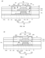
FIG. 2 is a schematic structural diagram of an array substrate according to some embodiments of the present disclosure. -
FIG. 3 is a schematic structural diagram of an array substrate according to other embodiments of the present disclosure. -
FIG. 4 is a schematic cross-sectional view of a display panel according to some embodiments of the present disclosure. -
FIG. 5 is a schematic cross-sectional view of a display panel according to other embodiments of the present disclosure. -
- 30, display panel; 10, array substrate; 201, light-emitting device layer; 2011, light-emitting device; 202, opposing substrate; 203, liquid crystal layer;
- 101, substrate; 102, buffer layer;
- 103a, first semiconductor layer; 103, first active layer; 1031, first channel portion; 1032a, first initial doped portion; 1032a1, first region; 1032a2, second region; 1032, first doped portion; 10321, first doped sub-portion; 10322, second doped sub-portion; 1033a, second initial doped portion; 1033, second doped portion;
- 1041, fourth insulating layer; 1042, first insulating layer; 1043, second insulating layer; 1044, third insulating layer;
- 105, first gate;
- 106a, second semiconductor layer; 106, second active layer; 1061, second channel portion; 1062, third doped portion; 1063, fourth doped portion;
- 107, second gate;
- 10a, first via; 10d, second via; 10b, third via; 10e, fourth via; 10c, fifth via; 10f, sixth via;
- 1081, source; 1082, drain;
- T1, first transistor; T2, second transistor.
- Hereinafter, technical solutions in embodiments of the present disclosure will be clearly and completely described with reference to the accompanying drawings in embodiments of the present disclosure. Apparently, the described embodiments include but are not limited to the embodiments of the present disclosure. Other embodiments that can be obtained by a person with ordinary skill in the art on the basis of the embodiments in the present disclosure without creative labor belong to the protection scope of the present disclosure.
- Referring to
FIGs. 1A to 1H , which are schematic structural diagrams of a process for manufacturing an array substrate according to some embodiments of the present disclosure. The process for manufacturing an array substrate according to some embodiments of the present disclosure is described in detail with reference toFIGs. 1A to 1H . - Referring to
FIG. 1A , firstly, forming afirst semiconductor layer 103a on thesubstrate 101. - In some embodiments, as shown in
FIG. 1A , before the step of forming afirst semiconductor layer 103a on thesubstrate 101, the process for manufacturing the array substrate further includes forming abuffer layer 102 on thesubstrate 101. - Illustratively, the
substrate 101 includes a glass substrate, but is not limited thereto. Thesubstrate 101 may also be a flexible substrate including a polymer layer. - Illustratively, the
buffer layer 102 includes, but is not limited to, a silicon oxide layer, a silicon nitride layer, a silicon oxynitride layer, or a stacked layer of a silicon nitride layer and a silicon oxide layer. - In some embodiments, the step of forming a
first semiconductor layer 103a on thesubstrate 101 includes forming afirst semiconductor layer 103a on a surface of thebuffer layer 102 away from thesubstrate 101. - In some embodiments, the
first semiconductor layer 103a is a single semiconductor layer. Materials of thefirst semiconductor layer 103a include amorphous silicon, polysilicon, or metal oxides. - Polysilicon can be obtained by subjecting amorphous silicon to laser annealing crystallization or other crystallization methods. The metal oxide includes at least one of indium element, zinc element, tungsten element, tin element, gallium element, and aluminum element. Illustratively, the material of the metal oxide includes, but is not limited to a metal oxide with low leakage current, such as indium gallium zinc oxide (IGZO), indium gallium tin oxide (IGTO), indium gallium oxide (IGO), indium zinc oxide (IZO), aluminum indium zinc oxide (AIZO), aluminum tin zinc oxide (ATZO), or the like.
- Next, referring to
FIG. 1B , forming afirst gate 105 overlapping with thefirst semiconductor layer 103a on one side of thefirst semiconductor layer 103a away from thesubstrate 101. - In some embodiments, as shown in
FIG. 1B , before the step of forming afirst gate 105 overlapping with thefirst semiconductor layer 103a on the side of thefirst semiconductor layer 103a away from thesubstrate 101, the process for manufacturing the array substrate further includes forming a fourthinsulating layer 1041 on thefirst semiconductor layer 103a. The fourthinsulating layer 1041 overlaps with part of thefirst semiconductor layer 103a. - The fourth
insulating layer 1041 is a first gate insulating layer. In some embodiments, the material of the fourthinsulating layer 1041 includes, but is not limited to, at least one of silicon oxide, aluminum oxide, and silicon nitride. Illustratively, the fourthinsulating layer 1041 includes a silicon oxide layer, or a stacked layer of an aluminum oxide layer, a silicon nitride layer and a silicon oxide layer, or a stacked of a silicon oxide layer, a silicon nitride layer and a silicon oxide layer. - In some embodiments, the step of forming a
first gate 105 overlapping thefirst semiconductor layer 103a on one side of thefirst semiconductor layer 103a away from thesubstrate 101 includes forming afirst gate 105 on one side of the fourthinsulating layer 1041 away from thesubstrate 101. - In some embodiments, the material of the
first gate 105 includes, but is not limited to, at least one of molybdenum, aluminum, copper, titanium, indium zinc oxide, and indium tin oxide. Illustratively, thefirst gate 105 includes a molybdenum layer (Mo), or a stacked layer of a molybdenum layer and an aluminum layer (Mo/Al), or a stacked layer of a molybdenum layer and a copper layer (Mo/Cu), or a stacked layer of a molybdenum-titanium alloy layer and a copper layer (MoTi/Cu), or a stacked layer of a molybdenum-titanium alloy layer, a copper layer, and a molybdenum-titanium alloy layer that are sequentially stacked (MoTi/Cu/MoTi), or a stacked layer of a titanium layer, an aluminum layer, and a titanium layer that are sequentially stacked (Ti/Al/Ti), or a stacked of a titanium layer, a copper layer, and a titanium layer that are sequentially stacked (Ti/Cu/Ti), or a stacked of a molybdenum layer, a copper layer, and an indium zinc oxide layer that are sequentially stacked (Mo/Cu/IZO), or a stacked layer of a zinc oxide layer, a copper layer, and a zinc oxide layer that are sequentially stacked (IZO/Cu/IZO). - Next, referring to
FIG. 1C , doping thefirst semiconductor layer 103a for the first time by using thefirst gate 105 as a mask, so that thefirst semiconductor layer 103a subjected to the first doping process is formed with a first initial dopedportion 1032a, a second initial dopedportion 1033a and afirst channel portion 1031. The first initial dopedportion 1032a and the second initial dopedportion 1033a are connected to opposite ends of thefirst channel portion 1031, respectively. - In some embodiments of the present disclosure, after the
first semiconductor layer 103a is doped for the first time by using thefirst gate 105 as a mask, the doped portions of thefirst semiconductor layer 103a form the first initial dopedportion 1032a and the second initial dopedportion 1033a, respectively, and the undoped portion of thefirst semiconductor layer 103a forms thefirst channel portion 1031. A doping concentration of ions in the first initial dopedportion 1032a is the same as that in the second initial dopedportion 1033a. Both the first initial dopedportion 1032a and the second initial dopedportion 1033a have conductivity. An orthographic projection of thefirst channel portion 1031 on thesubstrate 101 completely overlaps with an orthographic projection of thefirst gate 105 on thesubstrate 101. In other words, the orthographic projection of thefirst channel portion 1031 on thesubstrate 101 is basically the same as the the orthographic projection of thefirst gate 105 on thesubstrate 101. - In some embodiments, the length of the first initial doped
portion 1032a is greater than the length of the second initial dopedportion 1033a, and the length of the first initial dopedportion 1032a is long enough to facilitate subsequent differential design of the resistances in different regions of the first initial dopedportion 1032a. Meanwhile, in the direction perpendicular to the thickness of thesubstrate 101, that is, in the horizontal direction, a distance between an edge of thefirst gate 105 close to the first initial dopedportion 1032a and an edge of the first initial dopedportion 1032a away from thefirst channel portion 1031 is greater than a distance between an edge of thefirst gate 105 close to the second initial dopedportion 1033a and an edge of the second initial dopedportion 1033a away from thefirst channel portion 1031. - In other embodiments, the length of the first initial doped
portion 1032a may also be less than or equal to the length of the second initial dopedportion 1033a. - In some embodiments of the present disclosure, the first initial doped
portion 1032a has a first region 1032a1 and a second region 1032a2. The second region 1032a2 is located between the first region 1032a1 and thefirst channel portion 1031. For part of the first initial dopedportion 1032a located in the first region 1032a1, it is necessary to further perform process of doping ions. For part of the first initial dopedportion 1032a located in the second region 1032a2, no further process of doping ions is required. - In some embodiments, the first doping is N-type heavy doping or P-type heavy doping. N-type heavily doped ions include, but are not limited to, phosphorus ions. P-type heavily doped ions include, but are not limited to, boron ions.
- In some embodiments, the doping concentration of the first doping ranges from 1×10¹⁴/cm2 to 9×10¹⁴/cm2. Illustratively, the doping concentration of the first doping is 4×10¹⁴/cm2.
- Next, referring to
FIG. 1E , forming asecond semiconductor layer 106a on one side of thefirst gate 105 away from thesubstrate 101. Thesecond semiconductor layer 106a overlaps with thefirst channel portion 1031, the second region 1032a2, part of the first region 1032a1 and the second initial dopedportion 1033a. - In some embodiments, as shown in
FIG. 1D , before the step of forming asecond semiconductor layer 106a on one side of thefirst gate 105 away from thesubstrate 101, the process for manufacturing the array substrate further includes forming a first insulatinglayer 1042 covering thefirst gate 105, the first initial dopedportion 1032a, the second initial dopedportion 1033a and thebuffer layer 102, and forming a first via 10a overlapping with the second initial dopedportion 1033a in the first insulatinglayer 1042. - In some embodiments, the material of the first insulating
layer 1042 includes, but is not limited to, at least one of silicon oxide, silicon oxynitride, aluminum oxide, and silicon nitride. Illustratively, the first insulatinglayer 1042 includes any one of a silicon oxide layer, a silicon nitride layer, a silicon oxynitride layer, and or a stacked layer of a silicon nitride layer and a silicon oxide layer. - In some embodiments, referring to
FIG. 1E , the step of forming thesecond semiconductor layer 106a on the side of thefirst gate 105 away from thesubstrate 101 includes forming thesecond semiconductor layer 106a on the surface of the first insulatinglayer 1042 away from thesubstrate 101 and in the first via 10a. - Illustratively, the
second semiconductor layer 106a is a single semiconductor layer. The material of thesecond semiconductor layer 106a includes, but is not limited to, amorphous silicon, polysilicon, or metal oxides. The selection of the polysilicon and the metal oxides is as described above, and details are not described herein. - In some embodiments, the material of the
second semiconductor layer 106a is the same as, but not limited to, the material of thefirst semiconductor layer 103a. Illustratively, both thesecond semiconductor layer 106a and thefirst semiconductor layer 103a are metal oxide semiconductor layers. - In other embodiments, the material of the
second semiconductor layer 106a may be different from the material of thefirst semiconductor layer 103a. Illustratively, thefirst semiconductor layer 103a is a metal oxide semiconductor layer, and thesecond semiconductor layer 106a is a polysilicon semiconductor layer. - Next, referring to
FIGs. 1F and 1G , forming asecond gate 107 on one side of thesecond semiconductor layer 106a away from thesubstrate 101; and doping thesecond semiconductor layer 106a, part of the first initial dopedportion 1032a located in the first region 1032a1 and the second initial dopedportion 1033a for a second time by using thesecond gate 107 as a mask, so that the dopedsecond semiconductor layer 106a is formed with a secondactive layer 106, and part of the first initial dopedportion 1032a located in the first region 1032a1 and the second initial dopedportion 1033a form the first dopedsub-portion 10321 and the second dopedportion 1033, respectively. - In some embodiments of the present disclosure, before the step of forming the
second gate 107 on the side of thesecond semiconductor layer 106a away from thesubstrate 101, the process for manufacturing the array substrate further includes a step of forming a second insulatinglayer 1043 covering thesecond semiconductor layer 106a and the first insulatinglayer 1042. - The second insulating
layer 1043 is a second gate insulating layer. In some embodiments, the material of the second insulatinglayer 1043 includes, but is not limited to, at least one of silicon oxide, aluminum oxide, and silicon nitride. Illustratively, the second insulatinglayer 1043 includes a silicon oxide layer, or a stacked layer of an aluminum oxide layer, a silicon nitride layer and a silicon oxide layer, or a stacked layer of a silicon oxide layer, a silicon nitride layer and a silicon oxide layer. - In some embodiments of the present disclosure, after the
second semiconductor layer 106a, part of the first initial dopedportion 1032a located in the first region 1032a1 and the second initial dopedportion 1033a are doped for the second time by using thesecond gate 107 as a mask, the doped portions in thesecond semiconductor layer 106a form a thirddoped portion 1062 and a fourth dopedportion 1063, respectively; and the undoped portion in thesecond semiconductor layer 106a forms asecond channel portion 1061. The thirddoped portion 1062, and the fourth dopedportion 1063 are connected to opposite sides of thesecond channel portion 1061, respectively. Thesecond channel portion 1061, the thirddoped portion 1062, and the fourth dopedportion 1063 constitute the secondactive layer 106. - Furthermore, part of the first initial doped
portion 1032a located in the first region 1032a1 that is subjected to the second doping forms the first dopedsub-portion 10321. The second initial dopedportion 1033a that is subjected to the second doping forms the second dopedportion 1033. While part of the first initial dopedportion 1032a located in the second region 1032a2 that is not subjected to the second doping forms the second dopedsub-portion 10322. The first dopedsub-portion 10321 and the second dopedsub-portion 10322 constitute the first dopedportion 1032. The first dopedportion 1032, the second dopedportion 1033 and thefirst channel portion 1031 constitute the firstactive layer 103. - In some embodiments of the present disclosure, an orthographic projection of the
second channel portion 1061 on thesubstrate 101 completely overlaps with an orthographic projection of thesecond gate 107 on thesubstrate 101. In other words, the orthographic projection of thesecond channel portion 1061 on thesubstrate 101 is basically the same as the orthographic projection of thesecond gate 107 on thesubstrate 101. - In some embodiments of the present disclosure, the
second channel portion 1061 overlaps with thefirst channel portion 1031 and the second dopedsub-portion 10322; and the thirddoped portion 1062 overlaps with the second dopedportion 1033; so that thesecond channel portion 1061 overlaps with thefirst channel portion 1031, and the length of thesecond channel portion 1061 is greater than that of thefirst channel portion 1031, thereby facilitating the formation of the secondactive layer 106 and the firstactive layer 103 simultaneously by using a self-alignment process in combination with a process of doping ions by using thesecond gate 107 as a mask, thus further reducing the number of masks required for manufacturing the array substrate. - In some embodiments of the present disclosure, since the third
doped portion 1062 and the fourth dopedportion 1063 are formed by the same primary doping process with thesecond gate 107 as a mask, the doping concentration of ions in the thirddoped portion 1062 is the same as that in the fourth dopedportion 1063, and the thirddoped portion 1062 and the fourth dopedportion 1063 have conductivity due to the ions doped therein. Moreover, the thirddoped portion 1062 is contacted and connected with the second dopedportion 1033 through the first via 10a, so that wirings connecting the thirddoped portion 1062 and the second dopedportion 1033 are reduced, and the number of masks required for manufacturing the wirings is further reduced. - In some embodiments of the present disclosure, since both the first doped
sub-portion 10321 and the second dopedportion 1033 are formed through the first doping and the second doping, while the second dopedsub-portion 10322 is formed through only the first doping, the doping concentration of ions in the first dopedsub-portion 10321 is the same as that in the second dopedportion 1033, and the doping concentration of ions in the second dopedsub-portion 10322 is lower than that in the first dopedsub-portion 10321. As a result, the resistance of the second dopedsub-portion 10322 is greater than that of the first dopedsub-portion 10321, which reduces the voltage drop of the first dopedportion 1032 that needs to be connected to the drain. - In some embodiments of the present disclosure, a ratio of the doping concentration of ions in the second doped
sub-portion 10322 to the doping concentration of ions in the first dopedsub-portion 10321 is greater than or equal to 0.02 and less than or equal to 0.1, which can increase the resistance of the second dopedsub-portion 10322 while reduce the resistance of the first dopedsub-portion 10321, thus reducing the connection impedance between the first dopedsub-portion 10321 and the drain while reducing the voltage drop of the first dopedsub-portion 1032 that needs to be connected to the drain. - In some embodiments, both the first doping and the second doping are N-type heavy doping, or both the first doping and the second doping are P-type heavy doping.
- In some embodiments, the dopant ions used in first doping are the same as those in the second doping, but is not limited thereto, for example, the dopant ions used in first doping may also be different from those in the second doping.
- Illustratively, the second doping is N-type heavy doping or P-type heavy doping. N-type heavily doped ions include, but are not limited to, phosphorus ions. P-type heavily doped ions include, but are not limited to, boron ions. The doping concentration in the second doping ranges from 1×10¹⁴/cm2 to 9×10¹⁴/cm2.
- In some embodiments, the thickness of the second
active layer 106 is less than that of the firstactive layer 103, which is beneficial for the firstactive layer 103 to form a crystalline phase more easily during thermal annealing. - In some embodiments, after the step of forming the first
active layer 103 and the secondactive layer 106, the process for manufacturing the array substrate further includes subjecting the firstactive layer 103 to an annealing process to form a crystalline phase, and allowing the secondactive layer 106 to include an amorphous phase, so as to improve the performance stability of the firstactive layer 103 and maintain the semiconductor characteristics of the secondactive layer 106. - In some embodiments, after the step of doping the
second semiconductor layer 106a, part of the first initial dopedportion 1032a located in the first region 1032a1 and the second initial dopedportion 1033a for the second time, the process for manufacturing the array substrate further includes a step of forming a third insulatinglayer 1044 covering thesecond gate 107 and the second insulatinglayer 1043. - In some embodiments, referring to
FIG. 1G , after the step of forming the third insulatinglayer 1044 covering thesecond gate 107 and the second insulatinglayer 1043, a third via 10b, a fifth via 10c, and a second via 10d are formed. The third via 10b overlaps with the first dopedsub-portion 10321, and penetrates through the third insulatinglayer 1044, the second insulatinglayer 1043, and the first insulatinglayer 1042. The fifth via 10c overlaps with the fourth dopedportion 1063, and penetrates through the third insulatinglayer 1044 and the second insulatinglayer 1043. The second via 10d overlaps with the thirddoped portion 1062, and penetrates through the third insulatinglayer 1044 and the second insulatinglayer 1043. - In some embodiments, the third via 10b, the fifth via 10c, and the second via 10d are formed by using a process combing mask with etching, so as to reduce the number of masks required for manufacturing the array substrate.
- In some embodiments, referring to
FIG. 1H , forming asource 1081 and adrain 1082. Thedrain 1082 is formed in the third via 10b, in the fifth via 10c, and on a surface of the third insulatinglayer 1044 away from thesubstrate 101. Thesource 1081 is formed in the second via 10d, and on a surface of the third insulatinglayer 1044 away from thesubstrate 101. In this way, thedrain 1082 is connected to the fourth dopedportion 1063 and the first dopedsub-portion 10321, and thesource 1081 is connected to the thirddoped portion 1062 and the second dopedportion 1033. - In some embodiments, the materials of
source 1081 and drain 1082 include but are not limited to, at least one of molybdenum, aluminum, copper, titanium, indium zinc oxide, and indium tin oxide. Illustratively, thesource 1081 and thedrain 1082 include a molybdenum layer (Mo), or a stacked layer of a molybdenum layer and an aluminum layer (Mo/Al), or a stacked layer of a molybdenum layer and a copper layer (Mo/Cu), or a stacked layer of a molybdenum-titanium alloy layer and a copper layer (MoTi/Cu), or a stacked layer of a molybdenum-titanium alloy layer, a copper layer, and a molybdenum-titanium alloy layer that are sequentially stacked (MoTi/Cu/MoTi), or a stacked layer of a titanium layer, an aluminum layer, and a titanium layer that are sequentially stacked (Ti/Al/Ti), or a stacked of a titanium layer, a copper layer, and a titanium layer that are sequentially stacked (Ti/Cu/Ti), or a stacked of a molybdenum layer, a copper layer, and an indium zinc oxide layer that are sequentially stacked (Mo/Cu/IZO), or a stacked layer of a zinc oxide layer, a copper layer, and a zinc oxide layer that are sequentially stacked (IZO/Cu/IZO). - In some embodiments of the present disclosure, transistors are formed by the above method. The transistors include a first transistor T1 and a second transistor T2 disposed in parallel, so as to increase the mobility of the transistors. The first transistor T1 is a narrow channel transistor, which further increases the mobility of the transistor. The first transistor T1 includes a
source 1081, adrain 1082, a firstactive layer 103, and afirst gate 105. The second transistor T2 includes a secondactive layer 106, asecond gate 107, asource 1081, and adrain 1082. The first transistor T1 and the second transistor T2 are connected through the thirddoped portion 1062, and the first transistor T1 and the second transistor T2 share thesource 1081 and thedrain 1082, thereby saving the number of masks required for manufacturing the array substrate. Furthermore, the film layers of the first transistor T1 and the second transistor T2 are stacked, so that high mobility of the transistor is realized on the premise of reducing the horizontal space occupied by the transistors, the self-heating problem of the transistors is also improved, thus improving the performance stability of the transistors. - Referring to
FIG. 1H , which is a s schematic structural view of a display panel according to some embodiments of the present disclosure. Thearray substrate 10 includes asubstrate 101, a first transistor T1, and a second transistor T2. Both the first transistor T1 and the second transistor T2 are disposed on thesubstrate 101. - In some embodiments, the
array substrate 10 further includes abuffer layer 102 disposed between the first transistor T1 and thesubstrate 101. - The first transistor T1 includes a first
active layer 103, afirst gate 105, asource 1081, and adrain 1082. The firstactive layer 103 is disposed on thesubstrate 101. Thefirst gate 105 is disposed on one side of the firstactive layer 103. - Specifically, the
first gate 105 is disposed on one side of the firstactive layer 103 away from thesubstrate 101, that is, the first thin film transistor T1 is a top-gate thin film transistor, so that thefirst gate 105 can be used as a mask to form the firstactive layer 103 by doping with ions, thereby reducing the number of masks required for manufacturing thearray substrate 10. - In other embodiments, the
first gate 105 may also be disposed between the firstactive layer 103 and thesubstrate 101. In other words, the first transistor T1 may also be a bottom-gate thin film transistor. - In some embodiments, the first
active layer 103 includes a crystalline phase to improve the performance stability of the first transistor T1. - In some embodiments, the first
active layer 103 includes afirst channel portion 1031, a first dopedportion 1032, and a second dopedportion 1033, The first dopedportion 1032 and the second dopedportion 1033 are connected to opposite ends of thefirst channel portion 1031, respectively. Thefirst gate 105 overlaps with thefirst channel portion 1031. The first dopedportion 1032 includes a first dopedsub-portion 10321 and a second dopedsub-portion 10322, and the second dopedsub-portion 10322 is connected between thefirst channel portion 1031 and the first dopedsub-portion 10321. The doping concentration of ions in the second dopedsub-portion 10322 is less than that in the first dopedsub-portion 10321. The doping concentration of ions in the first dopedsub-portion 10321 is the same as that in the second dopedportion 1033. Thesource 1081 is connected to the second dopedportion 1033, and thedrain 1082 is connected to the first dopedsub-portion 10321 of the first dopedportion 1032. Due to this design, the resistance of the second dopedsub-portion 10322 is greater than that of the first dopedsub-portion 10321, which reduces the voltage drop of the first dopedportion 1032 connected to thedrain 1082, thereby improving the problem of poor stability caused by heat generation in the first transistor caused by hot carriers, and reducing the connection impedance between thedrain 1082 and the first dopedsub-portion 10321. - In some embodiments, along the direction in which the first
active layer 103 extends from the first dopedportion 1032 to the second dopedportion 1033, the length of the first dopedportion 1032 is greater than that of the second dopedportion 1033, so as to realize differential design of the resistances in different regions of the first dopedportion 1032 by adopting a process of doping ions. But it is not limited thereto. The length of the first dopedportion 1032 may also be less than or equal to that of the second dopedportion 1033. - In some embodiments, along the direction in which the first
active layer 103 extends from the first dopedportion 1032 to the second dopedportion 1033, the length of the first dopedportion 1032 is greater than that of the second dopedportion 1033, which can reduce the voltage drop of the first dopedportion 1032, so as to improve the problem of poor stability of the first transistor due to self-heating. Further, the overall resistance of the first dopedportion 1032 is small. - In some embodiments, the
array substrate 10 further includes a fourth insulatinglayer 1041, which is a first gate insulating layer. The fourth insulatinglayer 1041 is disposed between thefirst gate 105 and the firstactive layer 103. - In some embodiments, the
array substrate 10 further includes a first insulatinglayer 1042, which is an interlayer insulating layer. The first insulatinglayer 1042 covers thefirst gate 105, the firstactive layer 103, and thebuffer layer 102. - The second transistor T2 includes a second
active layer 106 and asecond gate 107. At least part of the secondactive layer 106 is located on one side of thefirst gate 105 away from thesubstrate 101. Specifically, part of the secondactive layer 106 is located on the surface of the first insulatinglayer 1042 away from thesubstrate 101. - The
second gate 107 is located on one side of the secondactive layer 106 away from thesubstrate 101, and overlaps with thesecond channel portion 1061, so that thesecond gate 107 can be used as a mask to form the secondactive layer 106 through a process of doping ions, thereby reducing the number of masks required for manufacturing thearray substrate 10. - The second
active layer 106 includes asecond channel portion 1061, a thirddoped portion 1062, and a fourth dopedportion 1063. The thirddoped portion 1062 and the fourth dopedportion 1063 are connected to opposite ends of thesecond channel portion 1061, respectively. - The third
doped portion 1062 is connected to the second dopedportion 1033 through the first viahole 10a penetrating through the first insulatinglayer 1042, so as to realize connection between the first transistor T1 and the second transistor T2, and reduce additional wirings required for connecting the thirddoped portion 1062 and the second dopedportion 1033, thereby further reducing the number of masks required for manufacturing thearray substrate 101. - The
second channel portion 1061 overlaps with thefirst channel portion 1031 and the second dopedsub-portion 10322. In other words, the length of thesecond channel portion 1061 is larger than that of thefirst channel portion 1031. The thirddoped portion 1062 overlaps with the second dopedportion 1033. The fourth dopedportion 1063 overlaps with the first dopedsub-portion 10321. Due to this design, it is convenient to use thesecond gate 107 as a mask to form the secondactive layer 106 through a process of doping ions, and at the same time to use thesecond gate 107 as a mask to form the first dopedsub-portion 10321 and the second dopedportion 1033, thereby further reducing the number of masks required for manufacturing the firstactive layer 103, and reducing the number of masks required for manufacturing thearray substrate 10. - In some embodiments, the second
active layer 106 includes an amorphous phase to ensure the switching performance of the second transistor T2. - In some embodiments, the thickness of the second
active layer 106 is less than that of the firstactive layer 103, which facilitates easier formation of the firstactive layer 103 including the crystalline phase during thermal annealing. - In some embodiments, the
array substrate 10 further includes a second insulatinglayer 1043 and a third insulatinglayer 1044. The second insulatinglayer 1043 is disposed between the secondactive layer 106 and thesecond gate 107. The thirdinsulating layer 1044 covers thesecond gate 107 and the second insulatinglayer 1043. - In some embodiments, the first transistor T1 is disposed in parallel with the second transistor T2, so as to increase the mobility of the transistors composed of the first transistor T1 and the second transistor T2.
- The
source 1081 and thedrain 1082 are located on one side of thesecond gate 107 away from thesubstrate 101, and both thesource 1081 and thedrain 1082 are located on the surface of the third insulatinglayer 1044 away from thesubstrate 101. - In some embodiments, the
drain 1082 is connected to the fourth dopedportion 1063 through the fifth via 10c penetrating through the third insulatinglayer 1044 and the second insulatinglayer 1043. Further, thedrain 1082 is connected to the first dopedsub-portion 10321 of the first dopedportion 1032 through the third via 10b penetrating through the third insulatinglayer 1044, the second insulatinglayer 1043 and the first insulatinglayer 1042. As a result, parallel connection between the first transistor T1 and the second transistor T2 can be realized. - In some embodiments, the
source 1081 is connected to the thirddoped portion 1062 through the second via 10d, and the thirddoped portion 1062 is connected to the second dopedportion 1033 through the first via 10a, so that thesource 1081 is connected to the second dopedportion 1033 through the thirddoped portion 1062, thereby further reducing the wirings connecting the first transistor T1 and the second transistor T2, reducing the number of masks required for manufacturing the wirings, and reducing the cost of manufacturing the array substrate. - Referring to
FIG. 2 , which is schematic cross-sectional view of a display panel according to other embodiments of the present disclosure. The array substrate shown inFIG. 2 is substantially similar to the array substrate shown inFIG. 1H , and details are not described. The differences lie in that the thirddoped portion 1062 is connected to the second dopedportion 1033 through the first via 10a, and the fourth dopedportion 1063 is connected to the first dopedsub-portion 10321 through the fourth via 10e, that is, the first transistor T1 and the second transistor T2 are connected in parallel through the thirddoped portion 1062 and the fourth dopedportion 1063 of the secondactive layer 106, so as to reduce wirings required fro connecting the first transistor T1 and the second transistor T2 in parallel, thereby further reducing the number of masks required for manufacturing the array substrate. The fourth via 10e penetrates through the first insulatinglayer 1042. - Referring to
FIG. 3 , which is schematic cross-sectional view of a display panel according to still other embodiments of the present disclosure. The array substrate shown inFIG. 3 is substantially similar to the array substrate shown inFIG. 1H , and details are not described. The differences lie in that thedrain 1082 is connected to the fourth dopedportion 1063 through the sixth via 10f, and the fourth dopedportion 1063 is connected to the first dopedsub-portion 10321 through the fourth via 10e. The sixth via 10f overlaps with the fourth dopedportion 1063, and penetrates through the third insulatinglayer 1044 and the second insulatinglayer 1043. The fourth via 10e overlaps with the first dopedsub-portion 10321 and penetrates through the first insulatinglayer 1042. - It should be noted that the first transistor T1 and the second transistor T2 may be connected in series.
- Referring to
FIGs. 4 and 5 , the present disclosure further provides adisplay panel 30 including thearray substrate 10 of any of the above-described embodiments. - Referring to
FIG. 4 , thedisplay panel 30 includes anarray substrate 10 and a light-emittingdevice layer 201. The light-emittingdevice layer 201 includes a light-emittingdevice 2011, and the light-emittingdevice 2011 is connected to at least one of the first transistor T1 and the second transistor T2. The light-emittingdevice 2011 includes, but is not limited to, at least one of an organic light-emitting diode, a quantum dot light-emitting diode, a micro light-emitting diode, and a sub-millimeter light-emitting diode. - Referring to
FIG. 5 , thedisplay panel 30 includes anarray substrate 10, an opposingsubstrate 202, and a liquid crystal layer 203, wherein the liquid crystal layer 203 is disposed between thearray substrate 10 and the opposingsubstrate 202. - Descriptions of the above embodiments are merely intended to help understand the technical solutions and core ideas of the present disclosure. A person with ordinary skill in the art should understand that various modifications may still be made to the technical solutions described in the foregoing embodiments, or equivalents may be made to some of the technical features therein. These modifications or substitutions do not depart the essence of the corresponding technical solutions from the scope of the technical solutions of the embodiments of the present disclosure.
Claims (10)
- An array substrate (10), characterized in that the array substrate (10) comprises:a substrate (101); anda first transistor (T1) disposed on the substrate (101);wherein the first transistor (T1) comprises:a first active layer (103) disposed on the substrate (101), and the first active layer (103) comprises a first channel portion (1031), a first doped portion (1032), and a second doped portion (1033); the first doped portion (1032) and the second doped portion (1033) are connected to opposite ends of the first channel portion (1031), respectively; the first doped portion (1032) comprises a first doped sub-portion (10321) and a second doped sub-portion (10322), and the second doped sub-portion (10322) is connected between the first channel portion (1031) and the first doped sub-portion (10321); a doping concentration of ions in the second doped sub-portion (10322) is less than a doping concentration of ions in the first doped sub-portion (10321), and the doping concentration of ions in the first doped sub-portion (10321) is the same as a doping concentration of ions in the second doped portion (1033);a first gate (105) disposed on one side of the first active layer (103), and the first gate (105) overlaps with the first channel portion (1031); anda source (1081) and a drain (1082), the source (1081) is connected to the second doped portion (1033) and the drain (1082) is connected to the first doped sub-portion (10321) of the first doped portion (1032).
- The array substrate (10) according to claim 1, characterized in that the first gate (105) is disposed on one side of the first active layer (103) away from the substrate (101);
the array substrate (10) further comprises a second transistor (T2), and the second transistor (T2) comprises:a second active layer (106), at least part of the second active layer (106) is disposed on one side of the first gate (105) away from the substrate (101); the second active layer (106) comprises a second channel portion (1061), a third doped portion (1062), and a fourth doped portion (1063); the third doped portion (1062) and the fourth doped portion (1063) are connected to opposite ends of the second channel portion (1061), respectively; the second channel portion (1061) overlaps with the first channel portion (1031) and the second doped portion (1033), the third doped portion (1062) overlaps with the second doped portion (1033), and the fourth doped portion (1063) overlaps with the first doped portion (1032); anda second gate (107), the second gate (107) is disposed on one side of the second active layer (106) away from the substrate (101) and overlaps with the second channel portion (1061). - The array substrate (10) according to claim 2, characterized in that the first transistor (T1) is connected in parallel with the second transistor (T2).
- The array substrate (10) according to claim 2, characterized in that the array substrate (10) further comprises a first insulating layer (1042) disposed between the first gate (105) and the second active layer (106), wherein the third doped portion (1062) is connected to the second doped portion (1033) through a first via (10a) penetrating through the first insulating layer (1042).
- The array substrate (10) according to any one of claims 2 to 4, characterized in that the array substrate (10) further comprises a second insulating layer (1043) disposed between the second active layer (106) and the second gate (107), and a third insulating layer (1044) covering the second gate (107), wherein the source (1081) is disposed on the third insulating layer (1044), and the source (1081) is connected to the third doped portion (1062) through a second via (10d) penetrating through the second insulating layer (1043) and the third insulating layer (1044).
- The array substrate (10) according to claim 5, characterized in that the drain (1082) is disposed on the third insulating layer (1044), and the drain (1082) is connected to the first doped sub-portion (10321) through a third via (10b) penetrating through the first insulating layer (1042), the second insulating layer (1043) and the third insulating layer (1044).
- The array substrate (10) according to claim 6, characterized in that the fourth doped portion (1063) is connected to the first doped sub-portion (10321) through a fourth via (10e) penetrating through the first insulating layer (1042).
- The array substrate (10) according to claim 6, characterized in that the array substrate (10) further comprises a fifth via (10c) penetrating through the second insulating layer (1043) and the third insulating layer (1044), wherein the drain (1082) is connected to the fourth doped portion (1063) through the fifth via (10c).
- The array substrate (10) according to claim 2, characterized in that a thickness of the second active layer (106) is less than that of the first active layer (103).
- A display panel (30), characterized in that the display panel (30) comprises the array substrate (10) according to any one of claims 1-9.
Applications Claiming Priority (1)
| Application Number | Priority Date | Filing Date | Title |
|---|---|---|---|
| CN202310828547.XA CN116544246A (en) | 2023-07-07 | 2023-07-07 | Array substrate and display panel |
Publications (1)
| Publication Number | Publication Date |
|---|---|
| EP4489074A1 true EP4489074A1 (en) | 2025-01-08 |
Family
ID=87458271
Family Applications (1)
| Application Number | Title | Priority Date | Filing Date |
|---|---|---|---|
| EP23193869.7A Pending EP4489074A1 (en) | 2023-07-07 | 2023-08-29 | Array substrate and display panel |
Country Status (5)
| Country | Link |
|---|---|
| US (1) | US20250015090A1 (en) |
| EP (1) | EP4489074A1 (en) |
| JP (1) | JP7640638B2 (en) |
| CN (1) | CN116544246A (en) |
| DE (1) | DE102023128884A1 (en) |
Citations (6)
| Publication number | Priority date | Publication date | Assignee | Title |
|---|---|---|---|---|
| US20080090344A1 (en) * | 2001-11-16 | 2008-04-17 | Semiconductor Energy Laboratory Co., Ltd. | Semiconductor device and manufacturing method thereof |
| US20140099766A1 (en) * | 2011-05-24 | 2014-04-10 | Sharp Kabushiki Kaisha | Method of manufacturing semiconductor device |
| US20160365430A1 (en) * | 2014-12-30 | 2016-12-15 | Boe Technology Group Co., Ltd. | Thin film transistor and manufacturing method thereof, array substrate and manufacturing method thereof |
| US20170301701A1 (en) * | 2016-04-15 | 2017-10-19 | Au Optronics Corporation | Active device |
| US20210193838A1 (en) * | 2019-12-20 | 2021-06-24 | Lg Display Co., Ltd. | Thin Film Transistor Array Substrate and Electronic Device Including the Same |
| US20230187559A1 (en) * | 2021-12-09 | 2023-06-15 | AUO Corporation | Semiconductor device |
Family Cites Families (21)
| Publication number | Priority date | Publication date | Assignee | Title |
|---|---|---|---|---|
| JP4531175B2 (en) | 1998-12-03 | 2010-08-25 | 株式会社半導体エネルギー研究所 | Method for manufacturing semiconductor device |
| JP4058847B2 (en) | 1999-03-25 | 2008-03-12 | セイコーエプソン株式会社 | Electro-optical device drive circuit, electro-optical device, and projection display device |
| JP2007251100A (en) | 2006-03-20 | 2007-09-27 | Epson Imaging Devices Corp | Electro-optical device, electronic device, and semiconductor device |
| JP5430846B2 (en) | 2007-12-03 | 2014-03-05 | 株式会社半導体エネルギー研究所 | Method for manufacturing semiconductor device |
| JP5956736B2 (en) | 2011-10-18 | 2016-07-27 | 日本放送協会 | Multilayer semiconductor device and manufacturing method thereof |
| JP6034048B2 (en) | 2012-04-23 | 2016-11-30 | 株式会社半導体エネルギー研究所 | Display device, electronic equipment |
| KR102397873B1 (en) * | 2014-02-24 | 2022-05-16 | 엘지디스플레이 주식회사 | Display device |
| KR102367215B1 (en) * | 2015-08-31 | 2022-02-24 | 엘지디스플레이 주식회사 | Organic Light Emitting Display Device |
| KR102571610B1 (en) * | 2017-02-13 | 2023-08-30 | 삼성디스플레이 주식회사 | Semiconductor device and method for fabricating the same |
| CN107154407A (en) * | 2017-05-17 | 2017-09-12 | 厦门天马微电子有限公司 | Laminated film transistor device and its manufacture method, display panel and display device |
| JP7171738B2 (en) | 2018-01-11 | 2022-11-15 | アプライド マテリアルズ インコーポレイテッド | Thin film transistor with metal oxide switch and small storage capacitor |
| KR102630641B1 (en) | 2018-01-25 | 2024-01-30 | 삼성디스플레이 주식회사 | Display apparatus and method of manufacturing thereof |
| EP3754638B1 (en) | 2018-02-14 | 2025-05-07 | Boe Technology Group Co., Ltd. | Shift register unit, gate driving circuit, display device, and driving method |
| JP2018200483A (en) | 2018-08-07 | 2018-12-20 | 株式会社半導体エネルギー研究所 | Display device |
| JP2020205388A (en) | 2019-06-19 | 2020-12-24 | 株式会社ジャパンディスプレイ | Semiconductor device |
| CN111668237B (en) * | 2020-06-17 | 2024-01-26 | 京东方科技集团股份有限公司 | A display substrate and its preparation method, driving method and display device |
| KR102675926B1 (en) * | 2020-06-30 | 2024-06-17 | 엘지디스플레이 주식회사 | Display apparatus |
| KR102698618B1 (en) * | 2020-10-20 | 2024-08-27 | 엘지디스플레이 주식회사 | Thin film transistor array substrate and electronic device including the same |
| US20230074433A1 (en) * | 2021-09-03 | 2023-03-09 | Lg Display Co., Ltd. | Thin film transistor substrate and display device comprising the same |
| CN115394787B (en) * | 2022-08-16 | 2026-01-23 | 武汉华星光电技术有限公司 | Array substrate and display panel |
| CN115425090B (en) * | 2022-08-30 | 2026-02-10 | 武汉华星光电技术有限公司 | Thin-film transistors and their electronic devices |
-
2023
- 2023-07-07 CN CN202310828547.XA patent/CN116544246A/en active Pending
- 2023-08-22 US US18/236,425 patent/US20250015090A1/en active Pending
- 2023-08-29 EP EP23193869.7A patent/EP4489074A1/en active Pending
- 2023-09-28 JP JP2023167881A patent/JP7640638B2/en active Active
- 2023-10-20 DE DE102023128884.9A patent/DE102023128884A1/en active Pending
Patent Citations (6)
| Publication number | Priority date | Publication date | Assignee | Title |
|---|---|---|---|---|
| US20080090344A1 (en) * | 2001-11-16 | 2008-04-17 | Semiconductor Energy Laboratory Co., Ltd. | Semiconductor device and manufacturing method thereof |
| US20140099766A1 (en) * | 2011-05-24 | 2014-04-10 | Sharp Kabushiki Kaisha | Method of manufacturing semiconductor device |
| US20160365430A1 (en) * | 2014-12-30 | 2016-12-15 | Boe Technology Group Co., Ltd. | Thin film transistor and manufacturing method thereof, array substrate and manufacturing method thereof |
| US20170301701A1 (en) * | 2016-04-15 | 2017-10-19 | Au Optronics Corporation | Active device |
| US20210193838A1 (en) * | 2019-12-20 | 2021-06-24 | Lg Display Co., Ltd. | Thin Film Transistor Array Substrate and Electronic Device Including the Same |
| US20230187559A1 (en) * | 2021-12-09 | 2023-06-15 | AUO Corporation | Semiconductor device |
Also Published As
| Publication number | Publication date |
|---|---|
| DE102023128884A1 (en) | 2025-01-09 |
| JP7640638B2 (en) | 2025-03-05 |
| JP2025009662A (en) | 2025-01-20 |
| CN116544246A (en) | 2023-08-04 |
| US20250015090A1 (en) | 2025-01-09 |
Similar Documents
| Publication | Publication Date | Title |
|---|---|---|
| US11869976B2 (en) | Thin film transistor and manufacturing method therefor, array substrate, and display device | |
| KR102055247B1 (en) | Tft array substrate, method for manufacturing the same, and display device | |
| KR100261983B1 (en) | Thin film transistor and liquid crystal display using the same | |
| KR20180020916A (en) | Thin film transistor and manufacturing method thereof | |
| CN106601786B (en) | Thin film transistor, method for making the same, and array substrate | |
| US20140203324A1 (en) | A strip-shaped gate-modulated tunneling field effect transistor and a preparation method thereof | |
| US10084095B2 (en) | Thin film transistor, method for manufacturing the same, and array substrate | |
| US9252284B2 (en) | Display substrate and method of manufacturing a display substrate | |
| CN113838930B (en) | Gallium nitride normally-off device with hybrid gate electrode structure and preparation method thereof | |
| US11031469B2 (en) | Semiconductor device, manufacturing method thereof, and electronic device including the same | |
| US12538506B2 (en) | Tunneling field effect transistor and manufacturing method thereof, display panel and display apparatus | |
| US20220399462A1 (en) | Thin film transistor and manufacturing method for the same | |
| US11616086B2 (en) | Thin film transistor panel, electric device including the same, and manufacturing method thereof | |
| US20250015090A1 (en) | Array substrate and display panel | |
| US20240429229A1 (en) | Gate-all-around transistor with hybrid conduction mechanism and manufacturing method thereof | |
| WO2023092478A1 (en) | Semiconductor device and manufacturing method therefor, and electronic apparatus | |
| JP3522440B2 (en) | Thin film semiconductor device | |
| KR20030025611A (en) | Method of fabricating CMOS Poly Silicon TFT having LDD structure | |
| US12142696B2 (en) | Thin film transistor, display apparatus, and method of fabricating thin film transistor | |
| JP2009141145A (en) | Semiconductor device, method for manufacturing the same, and display device | |
| JP2019106452A (en) | Semiconductor device and manufacturing method of the same | |
| CN114927532B (en) | Array substrate, manufacturing method thereof, and display panel | |
| CN121751656A (en) | Semiconductor device, manufacturing method thereof and electronic equipment | |
| CN120857804A (en) | Array substrate, manufacturing method thereof, and display device | |
| CN117476651A (en) | Array substrate, display panel and preparation method of array substrate |
Legal Events
| Date | Code | Title | Description |
|---|---|---|---|
| PUAI | Public reference made under article 153(3) epc to a published international application that has entered the european phase |
Free format text: ORIGINAL CODE: 0009012 |
|
| STAA | Information on the status of an ep patent application or granted ep patent |
Free format text: STATUS: REQUEST FOR EXAMINATION WAS MADE |
|
| 17P | Request for examination filed |
Effective date: 20230829 |
|
| AK | Designated contracting states |
Kind code of ref document: A1 Designated state(s): AL AT BE BG CH CY CZ DE DK EE ES FI FR GB GR HR HU IE IS IT LI LT LU LV MC ME MK MT NL NO PL PT RO RS SE SI SK SM TR |