EP4485527A1 - A method for manufacturing a semiconductor package assembly as well as a semiconductor package assembly obtained with this method - Google Patents
A method for manufacturing a semiconductor package assembly as well as a semiconductor package assembly obtained with this method Download PDFInfo
- Publication number
- EP4485527A1 EP4485527A1 EP23181337.9A EP23181337A EP4485527A1 EP 4485527 A1 EP4485527 A1 EP 4485527A1 EP 23181337 A EP23181337 A EP 23181337A EP 4485527 A1 EP4485527 A1 EP 4485527A1
- Authority
- EP
- European Patent Office
- Prior art keywords
- heat sink
- lead frame
- semiconductor package
- terminals
- semiconductor
- Prior art date
- Legal status (The legal status is an assumption and is not a legal conclusion. Google has not performed a legal analysis and makes no representation as to the accuracy of the status listed.)
- Granted
Links
Images



Classifications
-
- H—ELECTRICITY
- H10—SEMICONDUCTOR DEVICES; ELECTRIC SOLID-STATE DEVICES NOT OTHERWISE PROVIDED FOR
- H10W—GENERIC PACKAGES, INTERCONNECTIONS, CONNECTORS OR OTHER CONSTRUCTIONAL DETAILS OF DEVICES COVERED BY CLASS H10
- H10W70/00—Package substrates; Interposers; Redistribution layers [RDL]
- H10W70/40—Leadframes
- H10W70/421—Shapes or dispositions
- H10W70/424—Cross-sectional shapes
- H10W70/427—Bent parts
- H10W70/429—Bent parts being the outer leads
-
- H—ELECTRICITY
- H10—SEMICONDUCTOR DEVICES; ELECTRIC SOLID-STATE DEVICES NOT OTHERWISE PROVIDED FOR
- H10W—GENERIC PACKAGES, INTERCONNECTIONS, CONNECTORS OR OTHER CONSTRUCTIONAL DETAILS OF DEVICES COVERED BY CLASS H10
- H10W70/00—Package substrates; Interposers; Redistribution layers [RDL]
- H10W70/40—Leadframes
- H10W70/456—Materials
- H10W70/458—Materials of insulating layers on leadframes
-
- H—ELECTRICITY
- H10—SEMICONDUCTOR DEVICES; ELECTRIC SOLID-STATE DEVICES NOT OTHERWISE PROVIDED FOR
- H10W—GENERIC PACKAGES, INTERCONNECTIONS, CONNECTORS OR OTHER CONSTRUCTIONAL DETAILS OF DEVICES COVERED BY CLASS H10
- H10W74/00—Encapsulations, e.g. protective coatings
- H10W74/01—Manufacture or treatment
-
- H—ELECTRICITY
- H10—SEMICONDUCTOR DEVICES; ELECTRIC SOLID-STATE DEVICES NOT OTHERWISE PROVIDED FOR
- H10W—GENERIC PACKAGES, INTERCONNECTIONS, CONNECTORS OR OTHER CONSTRUCTIONAL DETAILS OF DEVICES COVERED BY CLASS H10
- H10W40/00—Arrangements for thermal protection or thermal control
- H10W40/20—Arrangements for cooling
- H10W40/22—Arrangements for cooling characterised by their shape, e.g. having conical or cylindrical projections
- H10W40/226—Arrangements for cooling characterised by their shape, e.g. having conical or cylindrical projections characterised by projecting parts, e.g. fins to increase surface area
- H10W40/228—Arrangements for cooling characterised by their shape, e.g. having conical or cylindrical projections characterised by projecting parts, e.g. fins to increase surface area the projecting parts being wire-shaped or pin-shaped
-
- H—ELECTRICITY
- H10—SEMICONDUCTOR DEVICES; ELECTRIC SOLID-STATE DEVICES NOT OTHERWISE PROVIDED FOR
- H10W—GENERIC PACKAGES, INTERCONNECTIONS, CONNECTORS OR OTHER CONSTRUCTIONAL DETAILS OF DEVICES COVERED BY CLASS H10
- H10W40/00—Arrangements for thermal protection or thermal control
- H10W40/70—Fillings or auxiliary members in containers or in encapsulations for thermal protection or control
- H10W40/77—Auxiliary members characterised by their shape
- H10W40/778—Auxiliary members characterised by their shape in encapsulations
-
- H—ELECTRICITY
- H10—SEMICONDUCTOR DEVICES; ELECTRIC SOLID-STATE DEVICES NOT OTHERWISE PROVIDED FOR
- H10W—GENERIC PACKAGES, INTERCONNECTIONS, CONNECTORS OR OTHER CONSTRUCTIONAL DETAILS OF DEVICES COVERED BY CLASS H10
- H10W70/00—Package substrates; Interposers; Redistribution layers [RDL]
- H10W70/01—Manufacture or treatment
- H10W70/04—Manufacture or treatment of leadframes
- H10W70/041—Connecting or disconnecting interconnections to or from leadframes, e.g. connecting bond wires or bumps
-
- H—ELECTRICITY
- H10—SEMICONDUCTOR DEVICES; ELECTRIC SOLID-STATE DEVICES NOT OTHERWISE PROVIDED FOR
- H10W—GENERIC PACKAGES, INTERCONNECTIONS, CONNECTORS OR OTHER CONSTRUCTIONAL DETAILS OF DEVICES COVERED BY CLASS H10
- H10W70/00—Package substrates; Interposers; Redistribution layers [RDL]
- H10W70/40—Leadframes
- H10W70/421—Shapes or dispositions
-
- H—ELECTRICITY
- H10—SEMICONDUCTOR DEVICES; ELECTRIC SOLID-STATE DEVICES NOT OTHERWISE PROVIDED FOR
- H10W—GENERIC PACKAGES, INTERCONNECTIONS, CONNECTORS OR OTHER CONSTRUCTIONAL DETAILS OF DEVICES COVERED BY CLASS H10
- H10W70/00—Package substrates; Interposers; Redistribution layers [RDL]
- H10W70/40—Leadframes
- H10W70/461—Leadframes specially adapted for cooling
-
- H—ELECTRICITY
- H10—SEMICONDUCTOR DEVICES; ELECTRIC SOLID-STATE DEVICES NOT OTHERWISE PROVIDED FOR
- H10W—GENERIC PACKAGES, INTERCONNECTIONS, CONNECTORS OR OTHER CONSTRUCTIONAL DETAILS OF DEVICES COVERED BY CLASS H10
- H10W70/00—Package substrates; Interposers; Redistribution layers [RDL]
- H10W70/40—Leadframes
- H10W70/464—Additional interconnections in combination with leadframes
-
- H—ELECTRICITY
- H10—SEMICONDUCTOR DEVICES; ELECTRIC SOLID-STATE DEVICES NOT OTHERWISE PROVIDED FOR
- H10W—GENERIC PACKAGES, INTERCONNECTIONS, CONNECTORS OR OTHER CONSTRUCTIONAL DETAILS OF DEVICES COVERED BY CLASS H10
- H10W70/00—Package substrates; Interposers; Redistribution layers [RDL]
- H10W70/40—Leadframes
- H10W70/464—Additional interconnections in combination with leadframes
- H10W70/466—Tape carriers or flat leads
-
- H—ELECTRICITY
- H10—SEMICONDUCTOR DEVICES; ELECTRIC SOLID-STATE DEVICES NOT OTHERWISE PROVIDED FOR
- H10W—GENERIC PACKAGES, INTERCONNECTIONS, CONNECTORS OR OTHER CONSTRUCTIONAL DETAILS OF DEVICES COVERED BY CLASS H10
- H10W70/00—Package substrates; Interposers; Redistribution layers [RDL]
- H10W70/40—Leadframes
- H10W70/481—Leadframes for devices being provided for in groups H10D8/00 - H10D48/00
-
- H—ELECTRICITY
- H10—SEMICONDUCTOR DEVICES; ELECTRIC SOLID-STATE DEVICES NOT OTHERWISE PROVIDED FOR
- H10W—GENERIC PACKAGES, INTERCONNECTIONS, CONNECTORS OR OTHER CONSTRUCTIONAL DETAILS OF DEVICES COVERED BY CLASS H10
- H10W72/00—Interconnections or connectors in packages
- H10W72/071—Connecting or disconnecting
-
- H—ELECTRICITY
- H10—SEMICONDUCTOR DEVICES; ELECTRIC SOLID-STATE DEVICES NOT OTHERWISE PROVIDED FOR
- H10W—GENERIC PACKAGES, INTERCONNECTIONS, CONNECTORS OR OTHER CONSTRUCTIONAL DETAILS OF DEVICES COVERED BY CLASS H10
- H10W74/00—Encapsulations, e.g. protective coatings
- H10W74/01—Manufacture or treatment
- H10W74/016—Manufacture or treatment using moulds
-
- H—ELECTRICITY
- H10—SEMICONDUCTOR DEVICES; ELECTRIC SOLID-STATE DEVICES NOT OTHERWISE PROVIDED FOR
- H10W—GENERIC PACKAGES, INTERCONNECTIONS, CONNECTORS OR OTHER CONSTRUCTIONAL DETAILS OF DEVICES COVERED BY CLASS H10
- H10W74/00—Encapsulations, e.g. protective coatings
- H10W74/10—Encapsulations, e.g. protective coatings characterised by their shape or disposition
- H10W74/111—Encapsulations, e.g. protective coatings characterised by their shape or disposition the semiconductor body being completely enclosed
-
- H—ELECTRICITY
- H10—SEMICONDUCTOR DEVICES; ELECTRIC SOLID-STATE DEVICES NOT OTHERWISE PROVIDED FOR
- H10W—GENERIC PACKAGES, INTERCONNECTIONS, CONNECTORS OR OTHER CONSTRUCTIONAL DETAILS OF DEVICES COVERED BY CLASS H10
- H10W90/00—Package configurations
- H10W90/811—Multiple chips on leadframes
-
- H—ELECTRICITY
- H10—SEMICONDUCTOR DEVICES; ELECTRIC SOLID-STATE DEVICES NOT OTHERWISE PROVIDED FOR
- H10W—GENERIC PACKAGES, INTERCONNECTIONS, CONNECTORS OR OTHER CONSTRUCTIONAL DETAILS OF DEVICES COVERED BY CLASS H10
- H10W74/00—Encapsulations, e.g. protective coatings
- H10W74/10—Encapsulations, e.g. protective coatings characterised by their shape or disposition
-
- H—ELECTRICITY
- H10—SEMICONDUCTOR DEVICES; ELECTRIC SOLID-STATE DEVICES NOT OTHERWISE PROVIDED FOR
- H10W—GENERIC PACKAGES, INTERCONNECTIONS, CONNECTORS OR OTHER CONSTRUCTIONAL DETAILS OF DEVICES COVERED BY CLASS H10
- H10W90/00—Package configurations
- H10W90/701—Package configurations characterised by the relative positions of pads or connectors relative to package parts
- H10W90/751—Package configurations characterised by the relative positions of pads or connectors relative to package parts of bond wires
- H10W90/754—Package configurations characterised by the relative positions of pads or connectors relative to package parts of bond wires between a chip and a stacked insulating package substrate, interposer or RDL
-
- H—ELECTRICITY
- H10—SEMICONDUCTOR DEVICES; ELECTRIC SOLID-STATE DEVICES NOT OTHERWISE PROVIDED FOR
- H10W—GENERIC PACKAGES, INTERCONNECTIONS, CONNECTORS OR OTHER CONSTRUCTIONAL DETAILS OF DEVICES COVERED BY CLASS H10
- H10W90/00—Package configurations
- H10W90/701—Package configurations characterised by the relative positions of pads or connectors relative to package parts
- H10W90/761—Package configurations characterised by the relative positions of pads or connectors relative to package parts of strap connectors
- H10W90/764—Package configurations characterised by the relative positions of pads or connectors relative to package parts of strap connectors between a chip and a stacked insulating package substrate, interposer or RDL
Definitions
- the present disclosure relates to a method for manufacturing a semiconductor package assembly consisting of a semiconductor package and a molding resin case.
- a method for manufacturing a semiconductor package assembly comprising the steps of i) forming at least one semiconductor package by means of the sub-steps i1) providing a lead frame made from a metal material having a first frame side and a second frame side opposite to the first frame side as well as having at least two terminals; i2) providing at least one semiconductor die structure having a first die side and a second die side opposite to the first die side with its second die side on the first frame side of the lead frame; i3) electrically and mechanically attaching the at least one semiconductor die structure to the terminals of the lead frame; i4) attaching a heat sink element on the first die side and/or the second die side of the semiconductor die structure; and ii) encapsulating the at least one semiconductor die structure, the heat sink element and the plurality of terminals with a molding resin leaving at least a portion of the heat sink and at least a portion of the at least two terminals exposed.
- the method further comprises the step of iii) providing, at least prior to the encapsulating step ii), a layer comprised of at least a silicate containing mineral on the lead frame and/or the semiconductor die structure adjacent to the heat sink element.
- silicate containing mineral mounted on the lead frame and/or the semiconductor die structure adjacent to the heat sink element shields the latter from the leads of the lead frame and provides an improved creepage performance, in particular for top cool semiconductor package assemblies having a top surface heat sink.
- the presence of such silicate containing mineral allows to increase the design margins of the semiconductor package assembly, as it would be possible to develop package assemblies with larger heatsinks for step-up thermal dissipation.
- step iii) is performed prior to step i2), and comprises providing an adhesive tape having an adhesive side and containing at least one layer comprised of the at least a silicate containing mineral on the adhesive side, and mounting at least the lead frame on the adhesive side of the adhesive tape.
- an adhesive tape as a back side tape in film-assisted molding techniques can support the manufacturability of thinner lead frames.
- step iii) is followed by the step of vi) removing the adhesive tape leaving the at least one layer comprised of the at least a silicate containing mineral exposed.
- the present disclosure also pertains to a semiconductor package assembly consisting of a semiconductor package and a molding resin case as manufactured in accordance with one or more of the method claims of the present disclosure.
- the semiconductor package at least comprises a lead frame made from a metal material having a first frame side and a second frame side opposite to the first frame side as well as having at least two terminals; at least one semiconductor die structure having a first die side and a second die side opposite to the first die side with its second die side on the first frame side of the lead frame; a plurality of connections electrically and mechanically connecting the at least one semiconductor die structure with the terminals of the lead frame; at least one heat sink element mounted to the semiconductor die structure; and at least one layer comprised of at least a silicate containing mineral at least adjacent to the at least one heat sink element; and a molding resin encapsulating the at least one semiconductor die structure, the at least one heat sink element, the plurality of terminals and the at least one layer comprised of at least a silicate containing mineral with a molding
- silicate containing mineral mounted on the lead frame and/or the semiconductor die structure adjacent to the heat sink element shields the latter from the leads of the lead frame and provides an improved creepage performance, in particular for top cool semiconductor package assemblies having a top surface heat sink.
- the presence of such silicate containing mineral allows to increase the design margins of the semiconductor package assembly, as it would be possible to develop package assemblies with larger heatsinks for step-up thermal dissipation.
- the silicate containing mineral is mica.
- Mica can be reinforced into a high stability composite, which provides a superior electrical insulation and is thus very useful in mitigating the risk of electrical arcing and creepage.
- the at least one layer comprised of the at least a silicate containing mineral layer surrounds the heat sink element.
- the at least one layer comprised of the at least a silicate containing mineral layer is positioned adjacent to the terminals of the lead frame.
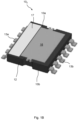
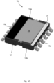
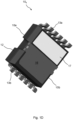
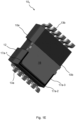
- Figures 1A-1F depict various examples of a semiconductor package assembly according to the disclosure, which are indicated with reference numerals 10 1 -10 6 , respectively.
- one critical property of semiconductor package assemblies for high voltage devices is the creepage and clearance distance of the metal parts within the semiconductor package assembly.
- the minimum creepage distance of electrical conductors is described, e.g. in IEC60664-1 and IPC2221A.
- the requirement for the minimum distances according to these standards is in contradiction to the trend for higher density electronics which require smaller package assemblies.
- the semiconductor package assemblies 10 1 -10 6 all consists of a semiconductor package 11 and a molding resin case 12, as shown in the cutaway Figure 1A .
- a heat sink element 16 is provided having a planar configuration with a first heat sink side 16a and a second heat sink side 16b opposite to the first heat sink side 16a.
- the heat sink element 16 may be mechanically connected with either the lead frame 14 (thereby contacting the first lead frame side 14a with its second heat sink side 16b), or with the semiconductor die structure 15 (thereby contacting the first die side 15a or second die side 15b with its second heat sink side 16b).
- the molding resin case 12 encapsulates at least the semiconductor die structure 15, the lead frame 14, the heat sink element 16 and the bond elements 130 and leaves a part of the bond element 130 partly exposed, thereby forming leads 13.
- the first heat sink side 16a of the encapsulated heat sink element 16 is also not encapsulated by the molding resin case 12, but is exposed similar as the leads 13.
- the exposed first heat sink side 16a of the heat sink element 16 allows for a proper heat dissipation.
- the encapsulated semiconductor die structure 15, the lead frame 14, the heat sink element 16, and the bond element 130 are considered a semiconductor package assembly 10 (10 1 -10 6 ).
- Such semiconductor package assembly 10 (10 1 -10 6 ) can be used in all kinds of electronics applications. To this end the semiconductor package assembly 10 (10 1 -10 6 ) can be mounted to a Printed Circuit Board, PCB, note shown, by soldering the leads 13 (13-13b) at the relevant mounting locations on the PCB.
- PCB Printed Circuit Board
- At least one layer 17, 17a-1, 17a-2, 17a-3 is provided which layer 17, 17a-1, 17a-2, 17a-3 is comprised of at least a silicate containing mineral.
- the at least one layer 17, 17a-1, 17a-2, 17a-3 comprised of at least a silicate containing mineral is provided at least adjacent to the heat sink element 16 and optionally also adjacent to the exposed leads 13a.
- the exposed leads 13b may be connected to the drain and are also electrically connected to the heat sink 16, as clearly depicted in Figure 1A . Accordingly, the leads 13b and the heat sink 16 are on the same potential level.
- the leads 13a are not electrically connected to the heat sink 16 and may be connected to the source and gate of the semiconductor die structure 15. The potential difference between the leads 13a and the heat sink 16 may induce a higher arcing risk and thermal build-up inside the package.
- the molding resin 12 also encapsulates the at least one layer 17, 17a, 17b, yet in an exposed manner similar to the heat sink element 16.
- silicate containing mineral 17, 17a-1, 17a-2, 17a-3 allows to increase the design margins of the semiconductor package assembly, as it would be possible to develop package assemblies with larger heatsinks for step-up thermal dissipation.
- the heat sink element 16 and the silicate containing mineral 17 are positioned at a first, top surface side 10a of the semiconductor package assemblies 10 1 , 10 2 and 10s, shielding the heat sink 16 from the leads 13a (which are on a different potential level than the heat sink 16).
- the heat sink element 16 and the silicate containing mineral 17 are positioned at a second, bottom surface side 10b of the semiconductor package assemblies 10a and 10s.
- the semiconductor package assemblies 10 1 -10 6 are to be mounted with their second, bottom surface side 10b on a PCB (no shown), and the silicate containing mineral 17 is electrically shielding the heat sink 16 from the leads 13a (which are on a different potential level than the heat sink 16), thereby limiting the risk of arcing.
- strips 17a-1, 17a-2, 17a-3 of silicate containing mineral are partially positioned around the heat sink 16 shielding the leads 13a (which are on a different potential level).
- the example of Figure 1F shows a leadless semiconductor package assembly 10 6 .
- the next step i3) pertains to electrically and mechanically attaching the at least one semiconductor die structure 15 to the terminals 13 of the lead frame 14, for example with the use of bond clips or bond wires 130.
- a heat sink element 16 is attached on the first die side 15a and/or the second die side 15b of the semiconductor die structure 15 or optionally to the lead frame 14.
- the method Prior to the encapsulating step ii) for encapsulating the at least one semiconductor die structure 15, the heat sink element 16, the lead frame 14 and the plurality of terminals 13 with a molding resin 12, the method performs the step iii) of providing a layer 17, 17a, 17b comprised of at least a silicate containing mineral on the lead frame 14 and/or the semiconductor die structure 15 adjacent to the heat sink element 16.
- Various techniques can be applied for providing the layer 17, 17a, 17b comprised of at least a silicate containing mineral on the lead frame 14 and/or the semiconductor die structure 15 adjacent to the heat sink element 16.
- One technique involves a printing technique of the silicate containing mineral into one or more overlapping layers 17, 17a, 17b.
- FIG. 2A Another technique is disclosed in Figure 2A .
- an adhesive tape 100 with an adhesive side 100a is provided on the adhesive side 199a.
- On the adhesive side 199a at least one layer 17, 17a, 17b comprised of the at least a silicate containing mineral is provided, for example with a length dimension more or less equal to a width dimension of the lead frame 14.
- the lead frame 14 is adhered with one of its a lead frame sides (here the second lead frame side 14b) on the adhesive side 100a of the adhesive tape 100, such the at least one layer 17, 17a, 17b of the at least a silicate containing mineral is sandwiched between the tape 100 and the lead frame 14.
- the previous outlined steps are performed: mounting the least one semiconductor die structure 15 with its second die side 15b on the first frame side 14a of the lead frame 14, for example at the location of a die paddle 14z (see Figure 2B ), electrically and mechanically attaching the at least one semiconductor die structure 15 to the terminals 13 of the lead frame 14 and attaching the at least one heat sink element 16 on the first die side 15a and/or the second die side 15b of the semiconductor die structure 15 or optionally to the lead frame 14.
- the encapsulating step is performed with the encapsulant 12 leaving the first heat sink side 16a of the heat sink element 16, optionally the layer 17, 17a, 17b of the at least a silicate containing mineral and the leads or terminals 13 exposed, thereby forming at least one encapsulated semiconductor package assembly 10 1 -10 6 .
- the efficiency of the manufacturing method according to the disclosure allows for manufacturing a large number of encapsulated semiconductor package assemblies 10 1 -10 6 , using an adhesive tape having an adhesive side and containing multiple layers, each comprised of the at least a silicate containing mineral on the adhesive side at certain locations conformal to the number semiconductor packages 11 to be formed on a matrix shaped lead frame 14 containing multiple die paddles 14z and leads 13.
- the individual semiconductor package assemblies 10 1 -10 6 can be created using known singulation and lead forming techniques.
Landscapes
- Structures Or Materials For Encapsulating Or Coating Semiconductor Devices Or Solid State Devices (AREA)
Abstract
Description
- The present disclosure relates to a method for manufacturing a semiconductor package assembly consisting of a semiconductor package and a molding resin case.
- One critical property of semiconductor package assemblies for high voltage devices (> 500V) is the creepage and clearance distance of the metal parts within the semiconductor package assembly. In high voltage applications the minimum creepage distance of electrical conductors is described, e.g. in IEC60664-1 and IPC2221A. The requirement for the minimum distances according to these standards is in contradiction to the trend for higher density electronics which require smaller package assemblies.
- In known power semiconductor devices no proper solution is yet presented which incorporate a superior electrical insulation to mitigate the risk of electrical arcing for surface mounted devices. Moreover, power semiconductor devices require a large exposed heatsink element for an effective thermal dissipation of heat being generated. However, at higher operating voltages, the arcing risk is higher and thermal build-up inside the package will increase as well.
- Accordingly, it is a goal of the present disclosure to provide an improved semiconductor package assembly capable of suppressing failures in case the distances as defined in the standard are violated e.g. due to limitations in package size.
- According to a first example of the disclosure, a method for manufacturing a semiconductor package assembly is proposed. The method comprising the steps of i) forming at least one semiconductor package by means of the sub-steps i1) providing a lead frame made from a metal material having a first frame side and a second frame side opposite to the first frame side as well as having at least two terminals; i2) providing at least one semiconductor die structure having a first die side and a second die side opposite to the first die side with its second die side on the first frame side of the lead frame; i3) electrically and mechanically attaching the at least one semiconductor die structure to the terminals of the lead frame; i4) attaching a heat sink element on the first die side and/or the second die side of the semiconductor die structure; and ii) encapsulating the at least one semiconductor die structure, the heat sink element and the plurality of terminals with a molding resin leaving at least a portion of the heat sink and at least a portion of the at least two terminals exposed. With the above steps at least one encapsulated semiconductor package assembly is formed.
- The method further comprises the step of iii) providing, at least prior to the encapsulating step ii), a layer comprised of at least a silicate containing mineral on the lead frame and/or the semiconductor die structure adjacent to the heat sink element.
- The silicate containing mineral mounted on the lead frame and/or the semiconductor die structure adjacent to the heat sink element, shields the latter from the leads of the lead frame and provides an improved creepage performance, in particular for top cool semiconductor package assemblies having a top surface heat sink. In addition, the presence of such silicate containing mineral allows to increase the design margins of the semiconductor package assembly, as it would be possible to develop package assemblies with larger heatsinks for step-up thermal dissipation.
- In a further example of the method according to the disclosure step iii) is performed prior to step i2), and comprises providing an adhesive tape having an adhesive side and containing at least one layer comprised of the at least a silicate containing mineral on the adhesive side, and mounting at least the lead frame on the adhesive side of the adhesive tape.
- The application of an adhesive tape as a back side tape in film-assisted molding techniques can support the manufacturability of thinner lead frames.
- In a further example, in the method according to the disclosure step iii) is followed by the step of vi) removing the adhesive tape leaving the at least one layer comprised of the at least a silicate containing mineral exposed.
- The present disclosure also pertains to a semiconductor package assembly consisting of a semiconductor package and a molding resin case as manufactured in accordance with one or more of the method claims of the present disclosure. In a particular example, the semiconductor package at least comprises a lead frame made from a metal material having a first frame side and a second frame side opposite to the first frame side as well as having at least two terminals; at least one semiconductor die structure having a first die side and a second die side opposite to the first die side with its second die side on the first frame side of the lead frame; a plurality of connections electrically and mechanically connecting the at least one semiconductor die structure with the terminals of the lead frame; at least one heat sink element mounted to the semiconductor die structure; and at least one layer comprised of at least a silicate containing mineral at least adjacent to the at least one heat sink element; and a molding resin encapsulating the at least one semiconductor die structure, the at least one heat sink element, the plurality of terminals and the at least one layer comprised of at least a silicate containing mineral with a molding resin leaving at least a portion of the heat sink and at least a portion of the at least two terminals exposed.
- The silicate containing mineral mounted on the lead frame and/or the semiconductor die structure adjacent to the heat sink element, shields the latter from the leads of the lead frame and provides an improved creepage performance, in particular for top cool semiconductor package assemblies having a top surface heat sink. In addition, the presence of such silicate containing mineral allows to increase the design margins of the semiconductor package assembly, as it would be possible to develop package assemblies with larger heatsinks for step-up thermal dissipation.
- Preferably, the silicate containing mineral is mica. Mica can be reinforced into a high stability composite, which provides a superior electrical insulation and is thus very useful in mitigating the risk of electrical arcing and creepage.
- In particular, creepage is further mitigated as in an example, the at least one layer comprised of the at least a silicate containing mineral layer surrounds the heat sink element.
- Alternatively, the at least one layer comprised of the at least a silicate containing mineral layer is positioned adjacent to the terminals of the lead frame.
- The disclosure will now be discussed with reference to the drawings, which show in:
-
Figures 1A-1F depict various examples of a singulated semiconductor package assembly according to the disclosure; -
Figures 2A-2D depict various manufacturing steps of a method according to the disclosure. - For a proper understanding of the disclosure, in the detailed description below corresponding elements or parts of the disclosure will be denoted with identical reference numerals in the drawings.
-
Figures 1A-1F depict various examples of a semiconductor package assembly according to the disclosure, which are indicated with reference numerals 101-106, respectively. - As outlined in the introduction, one critical property of semiconductor package assemblies for high voltage devices (> 500V) is the creepage and clearance distance of the metal parts within the semiconductor package assembly. In high voltage applications the minimum creepage distance of electrical conductors is described, e.g. in IEC60664-1 and IPC2221A. The requirement for the minimum distances according to these standards is in contradiction to the trend for higher density electronics which require smaller package assemblies.
- In known power semiconductor devices no proper solution is yet presented which incorporate a superior electrical insulation to mitigate the risk of electrical arcing for surface mounted devices. Moreover, power semiconductor devices require a large exposed heatsink element for an effective thermal dissipation of heat being generated. However, at higher operating voltages, the arcing risk is higher and thermal build-up inside the package will increase as well.
- Solutions for the above adverse effects of high voltages applied in a semiconductor package assembly according to the state of the art are depicted in the examples 101-106 of
Figures 1A-1F , respectively. The semiconductor package assemblies 101-106 all consists of asemiconductor package 11 and amolding resin case 12, as shown in the cutawayFigure 1A . - In all examples, the
semiconductor package 11 is composed of alead frame 14 having a firstlead frame side 14a and a secondlead frame side 14b opposite to the firstlead frame side 14a. Thelead frame 14 may also comprise at least two terminals, denoted as leads 13. Asemiconductor die structure 15 has afirst die side 15a and asecond die side 15b opposite to thefirst die side 15a and is mounted with itssecond die side 15b on the firstlead frame side 14a of thelead frame 14, for example at adie paddle 14z. In addition, one ormore bond elements 130 may be provided which are electrically connected with relevant parts of thesemiconductor die structure 15 with theleads 13. The bond elements may be bond clips of bond wires and extend into theleads 13. - In addition, a
heat sink element 16 is provided having a planar configuration with a firstheat sink side 16a and a secondheat sink side 16b opposite to the firstheat sink side 16a. Theheat sink element 16 may be mechanically connected with either the lead frame 14 (thereby contacting the firstlead frame side 14a with its secondheat sink side 16b), or with the semiconductor die structure 15 (thereby contacting thefirst die side 15a orsecond die side 15b with its secondheat sink side 16b). - As shown in
Figure 1A , themolding resin case 12 encapsulates at least thesemiconductor die structure 15, thelead frame 14, theheat sink element 16 and thebond elements 130 and leaves a part of thebond element 130 partly exposed, thereby formingleads 13. Moreover, the firstheat sink side 16a of the encapsulatedheat sink element 16 is also not encapsulated by themolding resin case 12, but is exposed similar as theleads 13. The exposed firstheat sink side 16a of theheat sink element 16 allows for a proper heat dissipation. The encapsulatedsemiconductor die structure 15, thelead frame 14, theheat sink element 16, and the bond element 130 (both its encapsulated part and exposed part, being the leads 13) are considered a semiconductor package assembly 10 (101-106). - Such semiconductor package assembly 10 (101-106) can be used in all kinds of electronics applications. To this end the semiconductor package assembly 10 (101-106) can be mounted to a Printed Circuit Board, PCB, note shown, by soldering the leads 13 (13-13b) at the relevant mounting locations on the PCB.
- In power semiconductor devices which are operated at higher operating voltages, the arcing risk is higher and the thermal build-up inside the package will increase as well. In order to suppress failures in case the distances as defined in the standard are violated e.g. due to limitations in package size and to mitigate the risk of electrical arcing for surface mounted devices, at least one
layer layer - As depicted in the
Figures 1A-1F , the at least onelayer heat sink element 16 and optionally also adjacent to the exposedleads 13a. - In this application it is observed that the exposed
leads 13b may be connected to the drain and are also electrically connected to theheat sink 16, as clearly depicted inFigure 1A . Accordingly, theleads 13b and theheat sink 16 are on the same potential level. Theleads 13a are not electrically connected to theheat sink 16 and may be connected to the source and gate of thesemiconductor die structure 15. The potential difference between theleads 13a and theheat sink 16 may induce a higher arcing risk and thermal build-up inside the package. - The
molding resin 12 also encapsulates the at least onelayer heat sink element 16. - The
silicate containing mineral lead frame 14 and/or thesemiconductor die structure 15 adjacent to theheat sink element 16 shields the latter from theleads 13a of thelead frame 14 and provides an improved creepage performance, in particular for top cool semiconductor package assemblies having a top surfaceheat sink element 16, as shown in the examples 101-106 of theFigures 1A-1F . - In addition, the presence of such
silicate containing mineral - In
Figures 1A ,1B and1C theheat sink element 16 and thesilicate containing mineral 17 are positioned at a first,top surface side 10a of thesemiconductor package assemblies heat sink 16 from theleads 13a (which are on a different potential level than the heat sink 16). In examples ofFigures 1D and1E theheat sink element 16 and thesilicate containing mineral 17 are positioned at a second,bottom surface side 10b of thesemiconductor package assemblies 10a and 10s. In all examples the semiconductor package assemblies 101-106 are to be mounted with their second,bottom surface side 10b on a PCB (no shown), and thesilicate containing mineral 17 is electrically shielding theheat sink 16 from theleads 13a (which are on a different potential level than the heat sink 16), thereby limiting the risk of arcing. Infigure 1E strips 17a-1, 17a-2, 17a-3 of silicate containing mineral are partially positioned around theheat sink 16 shielding theleads 13a (which are on a different potential level). In addition, the example ofFigure 1F , shows a leadlesssemiconductor package assembly 106. -
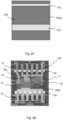
Figures 2A-2D depict various manufacturing steps of a method according to the disclosure. The method intends to form at least one semiconductor package 101-106 by means of the sub-steps of step i1) of providing alead frame 14 made from a metal material having afirst frame side 14a and asecond frame side 14b opposite to thefirst frame side 14a as well as having at least twoterminals 13; step i2) of providing at least onesemiconductor die structure 15 having afirst die side 15a and asecond die side 15b opposite to thefirst die side 15a with itssecond die side 15b on thefirst frame side 14a of thelead frame 14, for example at the location of adie paddle 14z (seeFigure 2B ). - The next step i3) pertains to electrically and mechanically attaching the at least one
semiconductor die structure 15 to theterminals 13 of thelead frame 14, for example with the use of bond clips orbond wires 130. Moreover, seeFigure 2B , in a next step i4) aheat sink element 16 is attached on thefirst die side 15a and/or thesecond die side 15b of the semiconductor diestructure 15 or optionally to thelead frame 14. - Prior to the encapsulating step ii) for encapsulating the at least one
semiconductor die structure 15, theheat sink element 16, thelead frame 14 and the plurality ofterminals 13 with amolding resin 12, the method performs the step iii) of providing alayer lead frame 14 and/or the semiconductor diestructure 15 adjacent to theheat sink element 16. - Various techniques can be applied for providing the
layer lead frame 14 and/or the semiconductor diestructure 15 adjacent to theheat sink element 16. - One technique involves a printing technique of the silicate containing mineral into one or more overlapping
layers - Another technique is disclosed in
Figure 2A . In the method step ofFigure 2A , anadhesive tape 100 with anadhesive side 100a is provided. On the adhesive side 199a at least onelayer lead frame 14. Thelead frame 14 is adhered with one of its a lead frame sides (here the secondlead frame side 14b) on theadhesive side 100a of theadhesive tape 100, such the at least onelayer tape 100 and thelead frame 14. - After the step of adhering the
lead frame 14 to theadhesive tape 100, the previous outlined steps are performed: mounting the least onesemiconductor die structure 15 with itssecond die side 15b on thefirst frame side 14a of thelead frame 14, for example at the location of adie paddle 14z (seeFigure 2B ), electrically and mechanically attaching the at least onesemiconductor die structure 15 to theterminals 13 of thelead frame 14 and attaching the at least oneheat sink element 16 on thefirst die side 15a and/or thesecond die side 15b of the semiconductor diestructure 15 or optionally to thelead frame 14. - Subsequently, the encapsulating step is performed with the
encapsulant 12 leaving the firstheat sink side 16a of theheat sink element 16, optionally thelayer terminals 13 exposed, thereby forming at least one encapsulated semiconductor package assembly 101-106. - The efficiency of the manufacturing method according to the disclosure allows for manufacturing a large number of encapsulated semiconductor package assemblies 101-106, using an adhesive tape having an adhesive side and containing multiple layers, each comprised of the at least a silicate containing mineral on the adhesive side at certain locations conformal to the
number semiconductor packages 11 to be formed on a matrix shapedlead frame 14 containing multiple diepaddles 14z and leads 13. - After encapsulation, the individual semiconductor package assemblies 101-106 can be created using known singulation and lead forming techniques.
-
- 101-106
- semiconductor package assembly (examples of the disclosure)
- 11
- semiconductor package
- 12
- molding resin case
- 13a-13b
- leads / terminals
- 130
- bond element
- 14
- lead frame
- 14a
- first side of lead frame
- 14b
- second side of lead frame
- 14z
- lead frame die paddle
- 15
- semiconductor die structure
- 15a
- first die side of semiconductor die structure
- 15b
- second die side of semiconductor die structure
- 16
- heat sink
- 16a
- first side of heat sink
- 16b
- second side of heat sink
- 17; 17a-n; 17b
- layer comprised of at least a silicate containing mineral
- 100
- tape
- 100a
- adhesive side of tape
Claims (10)
- A method for manufacturing a semiconductor package assembly, the method comprising the steps ofi) forming at least one semiconductor package by means of the sub-steps:i1) providing a lead frame made from a metal material having a first frame side and a second frame side opposite to the first frame side as well as having at least two terminals;i2) providing at least one semiconductor die structure having a first die side and a second die side opposite to the first die side with its second die side on the first frame side of the lead frame;i3) electrically and mechanically attaching the at least one semiconductor die structure to the terminals of the lead frame;i4) attaching a heat sink element on the first die side and/or the second die side of the semiconductor die structure;andii) encapsulating the at least one semiconductor die structure, the heat sink element and the plurality of terminals with a molding resin leaving at least a portion of the heat sink and at least a portion of the at least two terminals exposed, thereby forming at least one encapsulated semiconductor package assembly;
wherein the method further comprises the step of:iii) at least prior to the encapsulating step ii), providing a layer comprised of at least a silicate containing mineral on the lead frame and/or the semiconductor die structure adjacent to the heat sink element. - The method according to claim 1, wherein step iii) is performed prior to step i2), and comprisesproviding an adhesive tape having an adhesive side and containing at least one layer comprised of the at least a silicate containing mineral on the adhesive side, andmounting at least the lead frame on the adhesive side of the adhesive tape.
- The method according to claim 2, wherein step iii) is followed by the step of
vi) removing the adhesive tape leaving the at least one layer comprised of the at least a silicate containing mineral exposed. - The method according to any one or more of the preceding claims, wherein the silicate containing mineral is mica.
- The method according to any one or more of the preceding claims, wherein the at least one layer comprised of the at least a silicate containing mineral layer surrounds the heat sink element.
- The method according to any one or more of the preceding claims, wherein the at least one layer comprised of the at least a silicate containing mineral layer is adjacent to the terminals of the lead frame.
- A semiconductor package assembly consisting of a semiconductor package and a molding resin case as manufactured in accordance with one or more of the method claims 1-6, the semiconductor package at least comprising:a lead frame made from a metal material having a first frame side and a second frame side opposite to the first frame side as well as having at least two terminals;at least one semiconductor die structure having a first die side and a second die side opposite to the first die side with its second die side on the first frame side of the lead frame;a plurality of connections electrically and mechanically connecting the at least one semiconductor die structure with the terminals of the lead frame;at least one heat sink element mounted to the semiconductor die structure;at least one layer comprised of at least a silicate containing mineral at least adjacent to the at least one heat sink element; anda molding resin encapsulating the at least one semiconductor die structure, the at least one heat sink element, the plurality of terminals and the at least one layer comprised of at least a silicate containing mineral with a molding resin leaving at least a portion of the heat sink and at least a portion of the at least two terminals exposed.
- The semiconductor package assembly according to claim 7, wherein the silicate containing mineral is mica.
- The semiconductor package assembly according to claim 7 or 8, wherein the at least one layer comprised of the at least a silicate containing mineral layer is positioned around the heat sink element.
- The semiconductor package assembly according to claim 7, 8 or 9, wherein the at least one layer comprised of the at least a silicate containing mineral layer is positioned adjacent to the terminals of the lead frame.
Priority Applications (3)
| Application Number | Priority Date | Filing Date | Title |
|---|---|---|---|
| EP23181337.9A EP4485527B1 (en) | 2023-06-26 | 2023-06-26 | A method for manufacturing a semiconductor package assembly as well as a semiconductor package assembly obtained with this method |
| CN202410818838.5A CN119208159A (en) | 2023-06-26 | 2024-06-24 | Method for manufacturing a semiconductor package assembly and a semiconductor package assembly obtained by the method |
| US18/753,745 US20240429135A1 (en) | 2023-06-26 | 2024-06-25 | Method for manufacturing a semiconductor package assembly as well as a semiconductor package assembly obtained with this method |
Applications Claiming Priority (1)
| Application Number | Priority Date | Filing Date | Title |
|---|---|---|---|
| EP23181337.9A EP4485527B1 (en) | 2023-06-26 | 2023-06-26 | A method for manufacturing a semiconductor package assembly as well as a semiconductor package assembly obtained with this method |
Publications (2)
| Publication Number | Publication Date |
|---|---|
| EP4485527A1 true EP4485527A1 (en) | 2025-01-01 |
| EP4485527B1 EP4485527B1 (en) | 2026-02-25 |
Family
ID=87047925
Family Applications (1)
| Application Number | Title | Priority Date | Filing Date |
|---|---|---|---|
| EP23181337.9A Active EP4485527B1 (en) | 2023-06-26 | 2023-06-26 | A method for manufacturing a semiconductor package assembly as well as a semiconductor package assembly obtained with this method |
Country Status (3)
| Country | Link |
|---|---|
| US (1) | US20240429135A1 (en) |
| EP (1) | EP4485527B1 (en) |
| CN (1) | CN119208159A (en) |
Citations (3)
| Publication number | Priority date | Publication date | Assignee | Title |
|---|---|---|---|---|
| US5672910A (en) * | 1995-11-30 | 1997-09-30 | Mitsubishi Denki Kabushiki Kaisha | Semiconductor device and semiconductor module |
| US20170179009A1 (en) * | 2015-12-18 | 2017-06-22 | Infineon Technologies Austria Ag | Semiconductor devices with improved thermal and electrical performance |
| EP3428962A1 (en) * | 2016-03-07 | 2019-01-16 | Mitsubishi Electric Corporation | Semiconductor device and method for manufacturing semiconductor device |
-
2023
- 2023-06-26 EP EP23181337.9A patent/EP4485527B1/en active Active
-
2024
- 2024-06-24 CN CN202410818838.5A patent/CN119208159A/en active Pending
- 2024-06-25 US US18/753,745 patent/US20240429135A1/en active Pending
Patent Citations (3)
| Publication number | Priority date | Publication date | Assignee | Title |
|---|---|---|---|---|
| US5672910A (en) * | 1995-11-30 | 1997-09-30 | Mitsubishi Denki Kabushiki Kaisha | Semiconductor device and semiconductor module |
| US20170179009A1 (en) * | 2015-12-18 | 2017-06-22 | Infineon Technologies Austria Ag | Semiconductor devices with improved thermal and electrical performance |
| EP3428962A1 (en) * | 2016-03-07 | 2019-01-16 | Mitsubishi Electric Corporation | Semiconductor device and method for manufacturing semiconductor device |
Also Published As
| Publication number | Publication date |
|---|---|
| EP4485527B1 (en) | 2026-02-25 |
| US20240429135A1 (en) | 2024-12-26 |
| CN119208159A (en) | 2024-12-27 |
Similar Documents
| Publication | Publication Date | Title |
|---|---|---|
| US10056319B2 (en) | Power module package having patterned insulation metal substrate | |
| US9171773B2 (en) | Semiconductor device | |
| CN103339724B (en) | power semiconductor module | |
| CN102136472B (en) | Semiconductor apparatus module | |
| US9029995B2 (en) | Semiconductor device and method of manufacturing the same | |
| KR102172689B1 (en) | Semiconductor package and method of fabricating the same | |
| CN104517952B (en) | Power semiconductor module and method for producing a power semiconductor module | |
| KR20220007878A (en) | Electronic devices with double-sided cooling | |
| JP2010034350A (en) | Semiconductor device | |
| CN103858228B (en) | Semiconductor device and manufacture method thereof | |
| WO2007012911A1 (en) | Semiconductor module for a switched-mode power supply and method for its assembly | |
| JP6305176B2 (en) | Semiconductor device and manufacturing method | |
| JP6534677B2 (en) | Converter with partially thinned lead frame with stacked chips and interposer | |
| US11145578B2 (en) | Semiconductor package with top or bottom side cooling and method for manufacturing the semiconductor package | |
| US9905439B2 (en) | Power module package having patterned insulation metal substrate | |
| EP4485527B1 (en) | A method for manufacturing a semiconductor package assembly as well as a semiconductor package assembly obtained with this method | |
| CN107342275A (en) | Substrate, power module package and manufacturing method of patterned insulated metal substrate | |
| CN111834307B (en) | Semiconductor Module | |
| US9865531B2 (en) | Power module package having patterned insulation metal substrate | |
| EP4184566B1 (en) | A semiconductor device and a method of manufacturing such semiconductor device | |
| CN117293118A (en) | Power module and manufacturing method thereof | |
| CN202977407U (en) | Semiconductor module | |
| WO2022223199A1 (en) | Semiconductor power module and method for manufacturing a semiconductor power module | |
| US11217512B2 (en) | Semiconductor module | |
| EP4716452A1 (en) | A semiconductor package |
Legal Events
| Date | Code | Title | Description |
|---|---|---|---|
| PUAI | Public reference made under article 153(3) epc to a published international application that has entered the european phase |
Free format text: ORIGINAL CODE: 0009012 |
|
| STAA | Information on the status of an ep patent application or granted ep patent |
Free format text: STATUS: THE APPLICATION HAS BEEN PUBLISHED |
|
| AK | Designated contracting states |
Kind code of ref document: A1 Designated state(s): AL AT BE BG CH CY CZ DE DK EE ES FI FR GB GR HR HU IE IS IT LI LT LU LV MC ME MK MT NL NO PL PT RO RS SE SI SK SM TR |
|
| STAA | Information on the status of an ep patent application or granted ep patent |
Free format text: STATUS: REQUEST FOR EXAMINATION WAS MADE |
|
| 17P | Request for examination filed |
Effective date: 20250627 |
|
| GRAP | Despatch of communication of intention to grant a patent |
Free format text: ORIGINAL CODE: EPIDOSNIGR1 |
|
| STAA | Information on the status of an ep patent application or granted ep patent |
Free format text: STATUS: GRANT OF PATENT IS INTENDED |
|
| INTG | Intention to grant announced |
Effective date: 20251112 |
|
| GRAS | Grant fee paid |
Free format text: ORIGINAL CODE: EPIDOSNIGR3 |
|
| GRAA | (expected) grant |
Free format text: ORIGINAL CODE: 0009210 |
|
| STAA | Information on the status of an ep patent application or granted ep patent |
Free format text: STATUS: THE PATENT HAS BEEN GRANTED |
|
| AK | Designated contracting states |
Kind code of ref document: B1 Designated state(s): AL AT BE BG CH CY CZ DE DK EE ES FI FR GB GR HR HU IE IS IT LI LT LU LV MC ME MK MT NL NO PL PT RO RS SE SI SK SM TR |
|
| REG | Reference to a national code |
Ref country code: CH Ref legal event code: F10 Free format text: ST27 STATUS EVENT CODE: U-0-0-F10-F00 (AS PROVIDED BY THE NATIONAL OFFICE) Effective date: 20260225 Ref country code: GB Ref legal event code: FG4D |
|
| REG | Reference to a national code |
Ref country code: DE Ref legal event code: R096 Ref document number: 602023012474 Country of ref document: DE |
|
| REG | Reference to a national code |
Ref country code: IE Ref legal event code: FG4D |