EP4482285A1 - Informationsverarbeitungsvorrichtung, frequenzeinstellungsverfahren und frequenzeinstellungsprogramm - Google Patents
Informationsverarbeitungsvorrichtung, frequenzeinstellungsverfahren und frequenzeinstellungsprogramm Download PDFInfo
- Publication number
- EP4482285A1 EP4482285A1 EP22927081.4A EP22927081A EP4482285A1 EP 4482285 A1 EP4482285 A1 EP 4482285A1 EP 22927081 A EP22927081 A EP 22927081A EP 4482285 A1 EP4482285 A1 EP 4482285A1
- Authority
- EP
- European Patent Office
- Prior art keywords
- frequency
- quantum bit
- information processing
- signal
- processing apparatus
- Prior art date
- Legal status (The legal status is an assumption and is not a legal conclusion. Google has not performed a legal analysis and makes no representation as to the accuracy of the status listed.)
- Granted
Links
Images


Classifications
-
- G—PHYSICS
- G06—COMPUTING OR CALCULATING; COUNTING
- G06F—ELECTRIC DIGITAL DATA PROCESSING
- G06F1/00—Details not covered by groups G06F3/00 - G06F13/00 and G06F21/00
- G06F1/04—Generating or distributing clock signals or signals derived directly therefrom
- G06F1/12—Synchronisation of different clock signals provided by a plurality of clock generators
-
- G—PHYSICS
- G06—COMPUTING OR CALCULATING; COUNTING
- G06N—COMPUTING ARRANGEMENTS BASED ON SPECIFIC COMPUTATIONAL MODELS
- G06N10/00—Quantum computing, i.e. information processing based on quantum-mechanical phenomena
-
- G—PHYSICS
- G06—COMPUTING OR CALCULATING; COUNTING
- G06N—COMPUTING ARRANGEMENTS BASED ON SPECIFIC COMPUTATIONAL MODELS
- G06N10/00—Quantum computing, i.e. information processing based on quantum-mechanical phenomena
- G06N10/20—Models of quantum computing, e.g. quantum circuits or universal quantum computers
Definitions
- a quantum bit device to be used in a quantum computer using a superconducting circuit including a Josephson junction has been commonly known.
- harmonic noise generated by the digital signals may be superimposed on the microwaves.
- the present disclosure provides an information processing apparatus, a frequency adjustment method, and a frequency adjustment program capable of reducing harmonic noise superimposed on microwaves.
- an information processing apparatus including: a quantum bit; a digital circuit configured to generate a digital signal; a conversion circuit configured to convert the digital signal into a microwave to be transmitted to the quantum bit; and an adjustment circuit configured to set a first frequency of a clock used in the digital circuit such that a harmonic frequency of the first frequency differs from a second frequency of the microwave.
- harmonic noise superimposed on microwaves may be reduced.
- the information processing apparatus 100 processes information using a quantum bit 11 in accordance with a command cmd input from the computer 500.
- the information processing apparatus 100 is also called a quantum computer.
- the information processing apparatus 100 exemplified in FIG. 1 includes a cooler 10, a digital circuit 20, a conversion circuit 30, an adjustment circuit 40, a conversion circuit 50, and a digital circuit 60.
- the conversion circuit 30 converts the digital signals S generated by the digital circuit 20 into microwaves M to be transmitted to the cooler 10.
- a frequency of the microwaves M is higher than a frequency (use frequency f 0 ) used in the digital circuit 20.
- the use frequency f 0 is an example of a first frequency of a clock used in the digital circuit.
- the frequency of the microwaves M is an example of a second frequency of the microwaves transmitted to the quantum bit or the cooler.
- the quantum computer performs control using weak power of equal to or lower than -100 dBm.
- there is large noise such as digital noise.
- SNR signal-to-noise ratio
- ATT attenuator
- the power of the S component increases, whereby power consumption may increase.
- resolving power of lower bits of a digital-to-analog (DA) converter for converting digital signals into analog signals is wasted, and accordingly, a dynamic range may be narrowed.
- DA digital-to-analog
- the adjustment circuit 40 performs adjustment such that the multiplication of the use frequency f 0 differs from the microwaves M in the present embodiment. As a result, the factors of generating the harmonic noise superimposed on the microwaves M are reduced or removed, whereby the harmonic noise superimposed on the microwaves M may be reduced.
- the digital circuit 60 performs predetermined processing on the digital output signal B from the conversion circuit 50, and outputs it to the computer 500 as read data d.
- the resonance frequency of the quantum bit 11 may drift every manufacturing variation of the quantum bit 11 or every activation of the quantum bit 11.
- the adjustment circuit 40 may observe the output signal A for each activation of the quantum bit 11, and may adjust the frequency of the microwaves M to the resonance frequency of the quantum bit 11 for each activation of the quantum bit 11 so that the state of the quantum bit 11 is read from the output signal A.
- the read data d representing the read result of the state of the quantum bit 11 may be supplied to the computer 500, and the computer 500 is enabled to obtain the read data d from the digital circuit 60.
- the adjustment circuit 40 may adjust the use frequency f 0 such that the SNR of the microwaves M looped back before being input to the cooler 10 satisfies a predetermined reference value.
- the harmonics e.g., harmonics generated in the microwaves M by operation of software, etc.
- the adjustment circuit 40 may adjust the use frequency f 0 such that the SNR of the microwaves M looped back before being input to the cooler 10 satisfies a predetermined reference value.
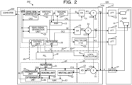
- FIG. 2 is a diagram illustrating a specific exemplary configuration of the information processing system including the information processing apparatus according to the embodiment illustrated in FIG. 1 .
- the information processing apparatus 100 includes the cooler 10 and a control device 300.
- the control device 300 is a device that controls the cooler 10 in accordance with the command cmd input from the computer 500.
- the control device 300 includes the digital circuit 20, the conversion circuit 30, the adjustment circuit 40, the conversion circuit 50, and the digital circuit 60.
- the control device 300 generates a plurality of microwaves M1, M2, and M3 having different frequencies in accordance with the command cmd input from the computer 500, and transmits them to the cooler 10.
- the microwave M1 is a control signal to be used to control the state of the quantum bit 11.
- the microwave M2 is a read signal to be used to read the state of the quantum bit 11.
- the microwave M3 is a pump signal to be used for an amplifier 14 that parametrically amplifies a signal representing the read result of the state of the quantum bit 11.
- the cooler 10 cools the quantum bit 11.
- the cooler 10 includes, for example, the quantum bit 11, attenuators (ATTs) 15, 16, and 17, and the amplifier 14.
- the quantum bit 11 includes a resonator 12 to be used to control the state of the quantum bit 11, and a resonator 13 to be used to read the state of the quantum bit 11.
- the attenuators 15, 16, and 17 attenuate the corresponding microwaves M1, M2, and M3, respectively.
- the amplifier 14 is a parametric amplifier that parametrically amplifies the signals representing the state of the quantum bit 11 read by the resonator 13.
- the digital circuit 20 generates the digital signals S in accordance with the command cmd input from the computer 500.
- the digital circuit 20 includes, for example, a control signal generation unit 21, a writing unit 22, a random access memory (RAM) 23, a reading unit 24, a read signal generation unit 25, a multiplication unit 26, and a control unit 27.
- the digital circuit 20 is implemented by, for example, a field programmable gate array (FPGA), an application specific integrated circuit (ASIC), a microcomputer, or the like.
- the control signal generation unit 21 generates a control signal for controlling the state of the quantum bit 11 in accordance with the command cmd input from the computer 500.
- the writing unit 22 temporarily stores the control signal generated by the control signal generation unit 21 in the RAM 23.
- the reading unit 24 reads the control signal from the RAM 23, and outputs the read control signal as a digital signal S1.
- the read signal generation unit 25 generates a read signal for reading the state of the quantum bit 11 in accordance with the command cmd input from the computer 500.
- the read signal generation unit 25 outputs the generated read signal as a digital signal S2.
- the control unit 27 controls frequency adjustment of a phase locked loop (PLL 42) in accordance with the command cmd input from the computer 500.
- the PLL 42 outputs the use frequency f 0 in accordance with the command cmd, and adjusts the use frequency f 0 to the frequency specified by the command cmd.
- the multiplication unit 26 generates clock signals CK0, CK1, and CK2 having frequencies obtained by multiplying the use frequency f 0 .
- the frequencies of the clock signals CK0, CK1, and CK2 are different from each other.
- the control signal generation unit 21 and the writing unit 22 operate according to the clock signal CK0 used in an interface with the computer 500.
- the reading unit 24 and a DA converter 31 operate according to the clock signal CK1 for DA conversion.
- a DA converter 33 operates according to the clock signal CK2 for DA conversion.
- the conversion circuit 30 includes the DA converter 31, a mixer 32, the DA converter 33, a mixer 34, and a multiplier 35.
- the DA converter 31 is a circuit that converts the digital signal S1 into an analog signal RF1.
- the analog signal RF1 is a radio frequency (RF) signal.
- a frequency of the analog signal RF1 changes as the use frequency f 0 changes.
- the mixer 32 up-converts the analog signal RF1 into the microwave M1 by multiplying the analog signal RF1 by a local oscillation signal LO1.
- the local oscillation signal LO1 has a frequency higher than that of the analog signal RF1.
- the DA converter 33 is a circuit that converts the digital signal S2 into an analog signal RF2.
- the analog signal RF2 is an RF signal.
- a frequency of the analog signal RF2 changes as the use frequency f 0 changes.
- the mixer 34 up-converts the analog signal RF2 into the microwave M2 by multiplying the analog signal RF2 by a local oscillation signal LO2.
- the local oscillation signal LO2 has a frequency higher than that of the analog signal RF2.
- the multiplier 35 generates the microwave M3 having a frequency twice the frequency of the microwave M2.
- the adjustment circuit 40 adjusts the use frequency f 0 such that the multiplication of the frequency of the analog signal RF1 differs from a predetermined frequency F1 (in this example, the resonance frequency of the resonator 12 used to control the state of the quantum bit 11). As a result, noise of a harmonic component that affects resonance of the resonator 12 may be reduced. Furthermore, the adjustment circuit 40 adjusts the use frequency f 0 such that the multiplication of the frequency of the analog signal RF2 differs from a predetermined frequency F2 (in this example, the resonance frequency of the resonator 13 used to read the state of the quantum bit 11). As a result, noise of a harmonic component that affects resonance of the resonator 13 may be reduced.
- the adjustment circuit 40 may include a local oscillator 41 that adjusts the frequency of the local oscillation signal LO1 input to the mixer 32 so that the frequency of the microwave M1 matches the predetermined frequency F1 (in this example, the resonance frequency of the resonator 12 used to control the state of the quantum bit 11).
- F1 the predetermined frequency
- F1 the resonance frequency of the resonator 12 used to control the state of the quantum bit 11
- the adjustment circuit 40 may include the local oscillator 41 that adjusts the frequency of the local oscillation signal LO2 input to the mixer 34 so that the frequency of the microwave M2 matches the predetermined frequency F2 (in this example, the resonance frequency of the resonator 13 used to read the state of the quantum bit 11).
- F2 the predetermined frequency
- F2 the resonance frequency of the resonator 13 used to read the state of the quantum bit 11
- the adjustment circuit 40 may include the local oscillator 41 that adjusts the frequency of the local oscillation signal LO2 input to the mixer 34 so that the frequency of the microwave M3 matches a predetermined frequency F3 (in this example, the frequency twice the resonance frequency of the resonator 13).
- F3 in this example, the frequency twice the resonance frequency of the resonator 13
- the adjustment circuit 40 includes the control unit 27, the local oscillator 41, and the PLL 42.
- the local oscillator 41 is an example of a first adjustment circuit that adjusts the frequencies of the microwaves, and in this example, it adjusts the frequencies of the microwaves M1, M2, and M3 according to a first frequency adjustment signal output from the control unit 27.
- the PLL 42 is an example of a second adjustment circuit that adjusts the use frequency f 0 , and in this example, it adjusts the use frequency f 0 according to a second frequency adjustment signal output from the control unit 27.
- the adjustment circuit 40 performs adjustment such that the multiplication of the use frequency f 0 differs from the frequencies of the microwaves M1, M2, and M3 using at least one of the local oscillator 41 or the PLL 42. As a result, the noise of the harmonic component that affects the control and reading of the quantum bit 11 may be reduced.
- the local oscillator 41 adjusts the frequencies of the microwaves M1, M2, and M3 to the respective predetermined frequencies F1, F2, and F3 corresponding thereto according to the first frequency adjustment signal output from the control unit 27.
- the PLL 42 adjusts the use frequency f 0 such that the multiplication of the use frequency f 0 differs from the predetermined frequencies F1, F2, and F3 according to the second frequency adjustment signal output from the control unit 27.
- the multiplication unit 26 multiplies the use frequency f 0 of 500 MHz by a factor of four and the DA converter 31 generates the analog signal RF1 of 2 GHz.
- the local oscillator 41 compensates for this difference in the frequency with the local oscillation signal LO1 in the microwave frequency band. Specifically, it is assumed that the frequency of the microwave M1 is adjusted to 10 GHz by the analog signal RF1 of 2 GHz and the local oscillation signal LO1 of 8 GHz.
- the PLL 42 changes the use frequency f 0 to 490 MHz, and the local oscillator 41 changes the frequency of the local oscillation signal LO1 to 8.04 GHz.
- the frequency of the microwave M1 is maintained at 10 GHz by the analog signal RF1 of 1.96 GHz and the local oscillation signal LO1 of 8.04 GHz.
- the other microwaves M2 and M3 are treated in a similar manner.
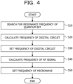
- FIG. 4 is a flowchart illustrating a first example of a frequency adjustment method.
- the frequency adjustment method illustrated in FIG. 4 is implemented by the control device 300 operating in accordance with the command cmd from the computer 500.
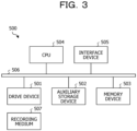
- a frequency adjustment program for causing the computer 500 to execute each processing illustrated in FIG. 4 is stored in the auxiliary storage device 502 described above.
Landscapes
- Engineering & Computer Science (AREA)
- Theoretical Computer Science (AREA)
- General Physics & Mathematics (AREA)
- Physics & Mathematics (AREA)
- General Engineering & Computer Science (AREA)
- Condensed Matter Physics & Semiconductors (AREA)
- Evolutionary Computation (AREA)
- Data Mining & Analysis (AREA)
- Mathematical Analysis (AREA)
- Mathematical Optimization (AREA)
- Pure & Applied Mathematics (AREA)
- Computing Systems (AREA)
- Computational Mathematics (AREA)
- Mathematical Physics (AREA)
- Software Systems (AREA)
- Artificial Intelligence (AREA)
- Stabilization Of Oscillater, Synchronisation, Frequency Synthesizers (AREA)
Applications Claiming Priority (1)
| Application Number | Priority Date | Filing Date | Title |
|---|---|---|---|
| PCT/JP2022/006386 WO2023157179A1 (ja) | 2022-02-17 | 2022-02-17 | 情報処理装置、周波数調整方法及び周波数調整プログラム |
Publications (3)
| Publication Number | Publication Date |
|---|---|
| EP4482285A1 true EP4482285A1 (de) | 2024-12-25 |
| EP4482285A4 EP4482285A4 (de) | 2025-03-19 |
| EP4482285B1 EP4482285B1 (de) | 2026-02-25 |
Family
ID=87577825
Family Applications (1)
| Application Number | Title | Priority Date | Filing Date |
|---|---|---|---|
| EP22927081.4A Active EP4482285B1 (de) | 2022-02-17 | 2022-02-17 | Informationsverarbeitungsvorrichtung, frequenzeinstellungsverfahren und frequenzeinstellungsprogramm |
Country Status (4)
| Country | Link |
|---|---|
| US (1) | US20250013902A1 (de) |
| EP (1) | EP4482285B1 (de) |
| JP (1) | JP7694793B2 (de) |
| WO (1) | WO2023157179A1 (de) |
Families Citing this family (1)
| Publication number | Priority date | Publication date | Assignee | Title |
|---|---|---|---|---|
| WO2026013819A1 (ja) * | 2024-07-10 | 2026-01-15 | Ntt株式会社 | 情報処理装置、パラメータ変換方法、及びプログラム |
Family Cites Families (5)
| Publication number | Priority date | Publication date | Assignee | Title |
|---|---|---|---|---|
| JP4777718B2 (ja) | 2005-08-11 | 2011-09-21 | 日本電信電話株式会社 | 量子ビット装置及び量子ビットの制御方法 |
| US10885460B2 (en) * | 2018-08-28 | 2021-01-05 | International Business Machines Corporation | Dispersive-resistive hybrid attenuator for quantum microwave circuits |
| US10922166B2 (en) * | 2019-03-27 | 2021-02-16 | Intel Corporation | Apparatus and method for probabilistic error correction of a quantum computing system |
| US10971593B2 (en) * | 2019-06-14 | 2021-04-06 | International Business Machines Corporation | Oxygen reservoir for low threshold voltage P-type MOSFET |
| US11509310B2 (en) * | 2019-06-17 | 2022-11-22 | Microsoft Technology Licensing, Llc | Charge locking circuits and control system for qubits |
-
2022
- 2022-02-17 WO PCT/JP2022/006386 patent/WO2023157179A1/ja not_active Ceased
- 2022-02-17 EP EP22927081.4A patent/EP4482285B1/de active Active
- 2022-02-17 JP JP2024500815A patent/JP7694793B2/ja active Active
-
2024
- 2024-08-01 US US18/791,820 patent/US20250013902A1/en active Pending
Also Published As
| Publication number | Publication date |
|---|---|
| JP7694793B2 (ja) | 2025-06-18 |
| WO2023157179A1 (ja) | 2023-08-24 |
| US20250013902A1 (en) | 2025-01-09 |
| EP4482285A4 (de) | 2025-03-19 |
| JPWO2023157179A1 (de) | 2023-08-24 |
| EP4482285B1 (de) | 2026-02-25 |
Similar Documents
| Publication | Publication Date | Title |
|---|---|---|
| US5764087A (en) | Direct digital to analog microwave frequency signal simulator | |
| US5898325A (en) | Dual tunable direct digital synthesizer with a frequency programmable clock and method of tuning | |
| US20090140896A1 (en) | Clock dithering process for reducing electromagnetic interference in d/a converters and apparatus for carrying out such process | |
| US8699985B1 (en) | Frequency generator including direct digital synthesizer and signal processor including the same | |
| US20250013902A1 (en) | Information processing apparatus, frequency adjustment method, and frequency adjustment program | |
| CN114744999A (zh) | 跳频源的实现方法、装置、跳频源、电子设备和存储介质 | |
| CN113162617B (zh) | 一种低相噪x波段频率源及其调制方法 | |
| US12123968B2 (en) | Systems and methods for digital signal chirp generation using frequency multipliers | |
| JPH0923158A (ja) | 周波数シンセサイザ | |
| US20090140820A1 (en) | Ring Oscillator with Constant Gain | |
| US12283964B2 (en) | Phase-locked loop frequency synthesizer and control method therefor | |
| US6859750B1 (en) | Ramp sweep synthesis control | |
| KR20230117827A (ko) | Dds 칩 동작을 위한 외부 기준 신호원 생성기 | |
| AU2003296435A1 (en) | Wideband dds synthesizer | |
| JPH08256058A (ja) | 信号発生装置 | |
| JP2022113497A (ja) | 周波数シンセサイザのクロック周波数を決定する方法 | |
| US20020064237A1 (en) | Quadrature modulation apparatus, radio transmission apparatus using quadrature modulation apparatus and quadrature modulation method | |
| RU2830675C1 (ru) | Синтезатор с низким уровнем фазовых шумов | |
| JP6428498B2 (ja) | 信号発生器 | |
| CN119675662B (zh) | 一种基于频率捷变雷达的频率源合成系统及方法 | |
| CN222850902U (zh) | 信号发生装置、量子计算测控系统及量子计算机 | |
| JP7807413B2 (ja) | 高周波信号発生装置 | |
| JP2026017025A (ja) | 処理装置、処理方法、およびプログラム | |
| CN121328758A (zh) | 一种任意微波信号的调制方法、装置和量子计算机 | |
| CN121328759A (zh) | 一种量子态驱动信号的补偿方法和装置 |
Legal Events
| Date | Code | Title | Description |
|---|---|---|---|
| STAA | Information on the status of an ep patent application or granted ep patent |
Free format text: STATUS: THE INTERNATIONAL PUBLICATION HAS BEEN MADE |
|
| PUAI | Public reference made under article 153(3) epc to a published international application that has entered the european phase |
Free format text: ORIGINAL CODE: 0009012 |
|
| STAA | Information on the status of an ep patent application or granted ep patent |
Free format text: STATUS: REQUEST FOR EXAMINATION WAS MADE |
|
| 17P | Request for examination filed |
Effective date: 20240806 |
|
| AK | Designated contracting states |
Kind code of ref document: A1 Designated state(s): AL AT BE BG CH CY CZ DE DK EE ES FI FR GB GR HR HU IE IS IT LI LT LU LV MC MK MT NL NO PL PT RO RS SE SI SK SM TR |
|
| A4 | Supplementary search report drawn up and despatched |
Effective date: 20250217 |
|
| RIC1 | Information provided on ipc code assigned before grant |
Ipc: G06F 1/12 20060101ALI20250211BHEP Ipc: G06N 10/00 20220101ALI20250211BHEP Ipc: H10N 60/10 20230101AFI20250211BHEP |
|
| DAV | Request for validation of the european patent (deleted) | ||
| DAX | Request for extension of the european patent (deleted) | ||
| REG | Reference to a national code |
Ref country code: DE Ref legal event code: R079 Free format text: PREVIOUS MAIN CLASS: H10N0060100000 Ipc: G06N0010000000 Ref country code: DE Ref legal event code: R079 Ref document number: 602022031394 Country of ref document: DE Free format text: PREVIOUS MAIN CLASS: H10N0060100000 Ipc: G06N0010000000 |
|
| GRAP | Despatch of communication of intention to grant a patent |
Free format text: ORIGINAL CODE: EPIDOSNIGR1 |
|
| STAA | Information on the status of an ep patent application or granted ep patent |
Free format text: STATUS: GRANT OF PATENT IS INTENDED |
|
| RIC1 | Information provided on ipc code assigned before grant |
Ipc: G06N 10/00 20220101AFI20251009BHEP Ipc: G06F 1/12 20060101ALI20251009BHEP Ipc: G06N 10/20 20220101ALI20251009BHEP |
|
| INTG | Intention to grant announced |
Effective date: 20251022 |
|
| GRAS | Grant fee paid |
Free format text: ORIGINAL CODE: EPIDOSNIGR3 |
|
| GRAA | (expected) grant |
Free format text: ORIGINAL CODE: 0009210 |
|
| STAA | Information on the status of an ep patent application or granted ep patent |
Free format text: STATUS: THE PATENT HAS BEEN GRANTED |
|
| AK | Designated contracting states |
Kind code of ref document: B1 Designated state(s): AL AT BE BG CH CY CZ DE DK EE ES FI FR GB GR HR HU IE IS IT LI LT LU LV MC MK MT NL NO PL PT RO RS SE SI SK SM TR |
|
| REG | Reference to a national code |
Ref country code: CH Ref legal event code: F10 Free format text: ST27 STATUS EVENT CODE: U-0-0-F10-F00 (AS PROVIDED BY THE NATIONAL OFFICE) Effective date: 20260225 Ref country code: GB Ref legal event code: FG4D |
|
| REG | Reference to a national code |
Ref country code: DE Ref legal event code: R096 Ref document number: 602022031394 Country of ref document: DE |
|
| REG | Reference to a national code |
Ref country code: IE Ref legal event code: FG4D |