EP4482016A1 - Dispositif de commande électronique - Google Patents
Dispositif de commande électronique Download PDFInfo
- Publication number
- EP4482016A1 EP4482016A1 EP22927133.3A EP22927133A EP4482016A1 EP 4482016 A1 EP4482016 A1 EP 4482016A1 EP 22927133 A EP22927133 A EP 22927133A EP 4482016 A1 EP4482016 A1 EP 4482016A1
- Authority
- EP
- European Patent Office
- Prior art keywords
- current
- load
- output
- control device
- electronic control
- Prior art date
- Legal status (The legal status is an assumption and is not a legal conclusion. Google has not performed a legal analysis and makes no representation as to the accuracy of the status listed.)
- Pending
Links
Images


Classifications
-
- G—PHYSICS
- G05—CONTROLLING; REGULATING
- G05F—SYSTEMS FOR REGULATING ELECTRIC OR MAGNETIC VARIABLES
- G05F1/00—Automatic systems in which deviations of an electric quantity from one or more predetermined values are detected at the output of the system and fed back to a device within the system to restore the detected quantity to its predetermined value or values, i.e. retroactive systems
- G05F1/10—Regulating voltage or current
- G05F1/46—Regulating voltage or current wherein the variable actually regulated by the final control device is DC
- G05F1/56—Regulating voltage or current wherein the variable actually regulated by the final control device is DC using semiconductor devices in series with the load as final control devices
- G05F1/577—Regulating voltage or current wherein the variable actually regulated by the final control device is DC using semiconductor devices in series with the load as final control devices for plural loads
-
- H—ELECTRICITY
- H02—GENERATION; CONVERSION OR DISTRIBUTION OF ELECTRIC POWER
- H02M—APPARATUS FOR CONVERSION BETWEEN AC AND AC, BETWEEN AC AND DC, OR BETWEEN DC AND DC, AND FOR USE WITH MAINS OR SIMILAR POWER SUPPLY SYSTEMS; CONVERSION OF DC OR AC INPUT POWER INTO SURGE OUTPUT POWER; CONTROL OR REGULATION THEREOF
- H02M1/00—Details of apparatus for conversion
- H02M1/0067—Converter structures employing plural converter units, other than for parallel operation of the units on a single load
- H02M1/008—Plural converter units for generating at two or more independent and non-parallel outputs, e.g. systems with plural point of load switching regulators
-
- H—ELECTRICITY
- H02—GENERATION; CONVERSION OR DISTRIBUTION OF ELECTRIC POWER
- H02M—APPARATUS FOR CONVERSION BETWEEN AC AND AC, BETWEEN AC AND DC, OR BETWEEN DC AND DC, AND FOR USE WITH MAINS OR SIMILAR POWER SUPPLY SYSTEMS; CONVERSION OF DC OR AC INPUT POWER INTO SURGE OUTPUT POWER; CONTROL OR REGULATION THEREOF
- H02M1/00—Details of apparatus for conversion
- H02M1/14—Arrangements for reducing ripples from DC input or output
-
- H—ELECTRICITY
- H02—GENERATION; CONVERSION OR DISTRIBUTION OF ELECTRIC POWER
- H02M—APPARATUS FOR CONVERSION BETWEEN AC AND AC, BETWEEN AC AND DC, OR BETWEEN DC AND DC, AND FOR USE WITH MAINS OR SIMILAR POWER SUPPLY SYSTEMS; CONVERSION OF DC OR AC INPUT POWER INTO SURGE OUTPUT POWER; CONTROL OR REGULATION THEREOF
- H02M7/00—Conversion of AC power input into DC power output; Conversion of DC power input into AC power output
- H02M7/42—Conversion of DC power input into AC power output without possibility of reversal
- H02M7/44—Conversion of DC power input into AC power output without possibility of reversal by static converters
- H02M7/48—Conversion of DC power input into AC power output without possibility of reversal by static converters using discharge tubes with control electrode or semiconductor devices with control electrode
- H02M7/53—Conversion of DC power input into AC power output without possibility of reversal by static converters using discharge tubes with control electrode or semiconductor devices with control electrode using devices of a triode or transistor type requiring continuous application of a control signal
- H02M7/537—Conversion of DC power input into AC power output without possibility of reversal by static converters using discharge tubes with control electrode or semiconductor devices with control electrode using devices of a triode or transistor type requiring continuous application of a control signal using semiconductor devices only, e.g. single switched pulse inverters
- H02M7/5387—Conversion of DC power input into AC power output without possibility of reversal by static converters using discharge tubes with control electrode or semiconductor devices with control electrode using devices of a triode or transistor type requiring continuous application of a control signal using semiconductor devices only, e.g. single switched pulse inverters in a bridge configuration
-
- H—ELECTRICITY
- H02—GENERATION; CONVERSION OR DISTRIBUTION OF ELECTRIC POWER
- H02P—CONTROL OR REGULATION OF ELECTRIC MOTORS, ELECTRIC GENERATORS OR DYNAMO-ELECTRIC CONVERTERS; CONTROLLING TRANSFORMERS, REACTORS OR CHOKE COILS
- H02P5/00—Arrangements specially adapted for regulating or controlling the speed or torque of two or more electric motors
- H02P5/68—Arrangements specially adapted for regulating or controlling the speed or torque of two or more electric motors controlling two or more DC dynamo-electric motors
Definitions
- the present invention relates to an electronic control device that drives an inductive load.
- an object of the present invention is to provide a highly reliable electronic control device that drives and controls a plurality of inductive loads and is capable of prolonging the life of electronic components by minimizing the total amount of effective ripple current values of the electronic components constituting the electronic control device.
- the present invention is configured as follows.
- An electronic control device that generates control signals for controlling a plurality of inductive loads includes a control unit configured to set drive output values including drive start timings, output duty ratios, and drive frequencies of a plurality of load drivers configured to drive the plurality of inductive loads based on various types of information related to drive states of the plurality of inductive loads, a current output unit configured to output current values flowing through the plurality of load drivers, and an ON timing setting unit configured to set a timing to turn on outputs of the drive output values in the plurality of load drivers based on the current values output by the current output unit.
- the ON timing setting unit sets ON timings of the plurality of load drivers so as to cancel out ripple current effective values generated in an electronic component connected by a power supply line as a drive source for the plurality of inductive loads.
- an electronic control device that drives and controls a plurality of inductive loads, it is possible to implement a highly reliable electronic control device capable of suppressing heat generation due to ripple currents in electronic components constituting the electronic control device and a control method thereof.
- FIGS. 1 to 6 An electronic control device according to a first embodiment of the present invention will be described with reference to FIGS. 1 to 6 .
- the electronic control device 110 to which the present invention is applied includes, as main components, an electronic component 120 such as an electrolytic capacitor for suppressing current fluctuation on a power supply 100 line, load drivers 160, 170, and 180 for driving a plurality of external inductive loads 130, 140, and 150, and an integrated circuit device 190 such as a microcontroller for controlling the load drivers 160, 170, and 180.
- an electronic component 120 such as an electrolytic capacitor for suppressing current fluctuation on a power supply 100 line
- load drivers 160, 170, and 180 for driving a plurality of external inductive loads 130, 140, and 150
- an integrated circuit device 190 such as a microcontroller for controlling the load drivers 160, 170, and 180.
- the load drivers 160, 170, 180 include any or all of the switching elements 200, 210, 220, and 230, such as MOS-FETs, for driving the external inductive loads 130, 140, and 150, such as electric motors.
- the integrated circuit device 190 includes, in addition to various calculations necessary for the operation of the electronic control device 110, a control unit 270 that sets load drive information from the drive states of the external inductive loads 130, 140, and 150 connected to the electronic control device 110, a current detection unit 280 that detects the output current values of the load drivers 160, 170, and 180, and an ON timing setting unit 290 that sets timings to turn on the outputs of the drive output values in the load drivers 160, 170, and 180 based on the output current values detected by the current detection unit 280.
- the PWM waveforms generated by the integrated circuit device 190 are input to the load drivers 160, 170, and 180.
- the switching elements included in the load drivers 160, 170, and 180 start ON/OFF operations based on the input PWM waveforms. By switching ON/OFF of the switching elements, output voltages 240, 250, and 260 of the load drivers 160, 170, and 180 are changed to drive the external inductive loads 130, 140, and 150.
- a current (a) flows from the power supply 100 toward the external inductive load 130, and the external inductive load 130 performs forward rotation operation.
- a current (b) flows from the power supply 100 toward the external inductive load 130, and the external inductive load 130 performs backward rotation operation.
- the control unit 270 in the integrated circuit device 190 sets load drive information such as the drive start timings, the PWM drive cycles, and the duty ratios of the load drivers 160, 170, and 180 based on various states related to the driving of the external inductive loads 130, 140, and 150 connected to the electronic control device 110.
- the current detection unit 280 detects output currents flowing through the load drivers 160, 170, and 180.
- a method of detecting output currents is configured to acquire, for example, peak values during a certain period in which the external inductive loads 130, 140, and 150 are driven.
- the method of detecting output currents according to the present invention is not limited to the acquisition of peak values in a certain period in which the external inductive loads 130, 140, and 150 are driven, and the same effect as those of the present invention can be obtained even when the method is applied to the electronic control device 110 having a similar program configuration for detecting the output currents of the load drivers 160, 170, and 180, such as the acquisition of average values in a certain period.
- the ON timing setting unit 290 sets the ON timings so as to cancel out ripple currents in the load drivers 160, 170, and 180 when the detected currents of the current detection unit 280 are large based on the load drive information set by the control unit 270 using the method in FIG. 5 to be described later.
- the ON timing setting unit 290 corrects the load drive information of the control unit 270 based on the ON timing set for each of the load drivers 160, 170, and 180.
- the integrated circuit device 190 generates control signals to the load drivers 160, 170, and 180 based on the corrected load drive information.
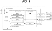
- FIG. 3 is a functional block diagram of the electronic control device 110.
- the integrated circuit device 190 includes a waveform generating unit 270W that generates a PWM waveform signal on the basis of a drive output value from the control unit 270 and a set value of the ON timing setting unit 290.
- the control unit 270 performs waveform forming processing by the waveform generating unit 270W and sets load drive information such as the drive start timings of the load drivers 160, 170, and 180, PWM drive cycles, and duty ratios based on various states related to the driving of the external inductive loads 130, 140, and 150 connected to the electronic control device 110.
- the current detection unit 280 detects output currents flowing through the load drivers 160, 170, and 180.
- the ON timing setting unit 290 sets ON timings so as to cancel ripple currents in the load drivers 160, 170, and 180 when the detected currents of the current detection units 280 are large.
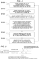
- step S100 in FIG. 4 the control unit 270 acquires various states regarding the driving of the external inductive loads 130, 140, and 150 connected to the electronic control device 110.
- step S110 the control unit 270 sets load drive information such as the drive start timings, the PWM drive cycles, and the duty ratios of the load drivers 160, 170, and 180 on the basis of the various states acquired in step S100.
- step S120 the current detection unit 280 detects output currents flowing through the load drivers 160, 170, and 180.
- step S130 in which on the basis of the load drive information set by the control unit 270, the ON timing setting unit 290 sets ON timings so as to cancel out ripple currents in the load drivers 160, 170, and 180 when the detected currents of the current detection units 280 are large.
- step S140 the ON timing setting unit 290 corrects the load drive information of the control unit 270 based on the ON timing set for each of the load drivers 160, 170, and 180.
- step S150 the integrated circuit device 190 generates control signals to the load drivers 160, 170, and 180 based on the load drive information corrected by the control unit 270 and ends the processing.
- FIG. 5 is an explanatory diagram of a control method for the electronic control device according to the first embodiment of the present invention.
- the current detection unit 280 detects output currents flowing through the load drivers 160, 170, and 180 and then transmits the detected currents to the ON timing setting unit 290. As illustrated in the table in FIG. 5 , the ON timing setting unit 290 ranks the load drivers 160, 170, and 180 in descending order of the output currents.
- the ON timing setting unit 290 sets the ON timings of the load drivers 160, 170, and 180 so as to cancel out the ripple current effective values generated in the electrolytic capacitor 120 such as an electronic component connected by a power supply line as a drive source for the loads.
- the ON timing of the first output voltage is set such that the ON/OFF timing of the output voltage of the load driver 180 having the first output current value coincides with the ON/OFF timing of the output voltage of the load driver 160 having the third output current value. Then, the ON timing of the first output voltage is set such that the ON/OFF timings of the first output voltage and the second output voltage coincide with each other.
- the ON timings of the output voltages set by circles 1 to 3 in FIG. 5 can be expressed as follows.
- the method for ripple current cancellation according to the present invention is not limited to (1) to (3) described above and may be based on the relationship illustrated in FIG. 6 . That is, as illustrated in FIG. 6 , in the relationship between a certain driver a and a certain driver b, the range in which transient response times t1 and t2 corresponding to the rising or falling instruction value of the output voltage of the driver a and transient response times t3 and t4 corresponding to the falling or rising instruction value of the output voltage of the driver b overlap may satisfy t1 - t3 ⁇ 0 and t1 - t4 ⁇ 0 illustrated in (A) and (C) or t2 - t4 ⁇ 0 and t2 - t3 ⁇ 0 illustrated in (B).
- the electronic control device 110 includes the plurality of load drive circuits (the load drivers 160, 170, and 180), the integrated circuit device 190 that transmits control signals to the plurality of load drive circuits (the load drivers 160, 170, and 180), the control unit 270 that sets drive output values including drive start timings, output duty ratios, and drive frequencies of the load drive circuits (the load drivers 160, 170, and 180) on the basis of various types of information regarding the drive states of the plurality of loads (130, 140, and 150), the current detection unit 280 that detects the output current values of the plurality of load drive circuits (the load drivers 160, 170, and 180), and the ON timing setting unit 290 that sets timings to turn on the outputs of the drive output values in the plurality of load drive circuits (the load drivers 160, 170, and 180) on the basis of the output current values detected by the current detection unit.
- the control unit 270 that sets drive output values including drive start timings, output duty ratios, and drive frequencies of the load drive circuits (the load
- the ON timing setting unit 290 sets the ON timings of the plurality of load drive circuits (130, 140, and 150) so as to cancel out the ripple current effective values generated in the electronic component 120 such as the electrolytic capacitor connected by the power supply line as a drive source for the plurality of loads (the load drivers 160, 170, and 180).
- the electronic control device 110 of the first embodiment by matching the ON/OFF timings of the output voltages 240, 250, and 260 of the load drivers 160, 170, and 180 depending on the magnitudes of the output currents, it is possible to cancel out ripple currents in the electronic component 120 such as an electrolytic capacitor and suppress heat generation, thereby implementing a highly reliable electronic control device.
- the order of the ON timings of the load drivers 160, 170, and 180 can be set in the descending order of the current values of the load drivers 160, 170, and 180.
- An electronic control device 110 according to a second embodiment of the present invention will be described with reference to FIG. 7 .
- FIG. 7 is a functional block diagram of the electronic control device 110 according to the second embodiment, which corresponds to a modification of the first embodiment ( FIG. 3 ) .
- the control unit 270 sets load drive information such as the drive start timings, the PWM drive cycles, and the duty ratios of the load drivers 160, 170, and 180 based on various states related to the drive of the external inductive loads 130, 140, and 150 connected to the electronic control device 110.
- the current detection unit 280 detects output currents flowing through the load drivers 160, 170, and 180.
- the ON timing setting unit 290 is configured to set ON timings so as to cancel out the ripple currents of the load drivers 160, 170, and 180 when the detected currents of the current detection units 280 are large based on the load drive information set by the control unit 270.
- the second embodiment illustrated in FIG. 7 is an embodiment configured to include a current estimation unit 300 that estimates the output currents of load drivers 160, 170, and 180 on the basis of information such as the duty ratios and the load constants of external inductive loads 130, 140, and 150 instead of causing the current detection unit 280 to detect output currents flowing through the load drivers 160, 170, and 180.
- a current estimation unit 300 that estimates the output currents of load drivers 160, 170, and 180 on the basis of information such as the duty ratios and the load constants of external inductive loads 130, 140, and 150 instead of causing the current detection unit 280 to detect output currents flowing through the load drivers 160, 170, and 180.
- an integrated circuit device 190 includes the current estimation unit 300 that estimates output currents of the load drivers 160, 170, and 180 from duty ratio information of the external inductive loads 130, 140, and 150 and load constant information including inductances and resistances.
- the duty ratio information of the external inductive loads 130, 140, and 150 and the load constant information including inductances and resistances are stored in, for example, a storage element such as a ROM 330 of the integrated circuit device 190.
- An ON timing setting unit 290 sets ON timings in the load drivers 160, 170, and 180 based on the output currents estimated by the current estimation unit 300.
- Other configurations are similar to those in FIG. 3 , and detailed description thereof will be omitted.
- the current estimation unit 300 estimates output currents instead of causing the current detection unit 280 to detect output currents flowing through the load drivers 160, 170, and 180 as in the first embodiment.
- the second embodiment can obtain an effect similar to that of the first embodiment and has an effect of lowering the processing load required for the integrated circuit device 190 and increasing the processing speed as compared with the first embodiment.
- An electronic control device 110 according to a third embodiment of the present invention will be described with reference to FIG. 8 .
- FIG. 8 is a functional block diagram of the electronic control device 110 according to the third embodiment, which corresponds to a modification of the first embodiment ( FIG. 3 ) .
- an ON timing setting unit 290 sets ON timings in load drivers 160, 170, and 180 based on the output currents estimated by a current detection unit 280, a threshold for output currents is set, and a driver through which a current equal to or less than the set threshold flows is excluded from the ON timing setting targets.
- Other configurations are similar to those of the first embodiment ( FIG. 3 ) and the second embodiment ( FIG. 7 ).
- an integrated circuit device 190 includes a current threshold determination unit 310 that determines whether output currents flowing through the load drivers 160, 170, and 180 exceed a set threshold.
- a set threshold is determined from, for example, the duty ratios and the load constant information of external inductive loads 130, 140, and 150 as described in the second embodiment and is stored in, for example, a storage element such as a ROM 330 in an integrated circuit device 190.
- the current threshold value comparison unit 310 excludes driver 1 (160) from the ON timing setting targets of the ON timing setting unit 290.
- Other configurations are similar to those of the first embodiment illustrated in FIG. 3 , and a detailed description thereof will be omitted.
- the electronic control device 110 is configured to exclude any of the load drivers 160, 170, and 180 whose output current is equal to or less than a set threshold value from the ON timing setting targets of the ON timing setting unit 290. This makes it possible to obtain the same effects as those of the first embodiment. In addition, as compared with the first embodiment, it is possible to reduce the processing load necessary for the integrated circuit device 190 and suppress the influence of shifting the ON timings of the external inductive loads 130, 140, and 150 on the control.
- FIG. 9 is a functional block diagram of the electronic control device 110 according to the fourth embodiment, which corresponds to a modification of the first embodiment ( FIG. 3 ).
- FIG. 10 is a timing chart of the operation of the fourth embodiment in a case where, for example, there are three external inductive loads.
- an ON timing setting unit 290 sets ON timings for canceling out ripple currents, including a combination of ON timings upon addition/subtraction of the driver currents detected by a current detection unit 280.
- Other configurations are similar to those of the first embodiment ( FIG. 3 ), the second embodiment ( FIG. 7 ), and the third embodiment ( FIG. 8 ).
- the integrated circuit device 190 includes a current calculation unit 320 that adds/subtracts output currents flowing through the load drivers 160, 170, and 180.
- FIG. 10 is a timing chart illustrating a control method for the electronic control device 110 according to the fourth embodiment of the present invention.
- the example illustrated in FIG. 10 is an example in a case where the current values detected by the current detection unit 280 are as follows. That is, the detected current of the load driver 160 is 0.8 A, the detected current of the load driver 170 is 0.5 A, and the detected current of the load driver 180 is 0.3 A. Then, the current calculation unit 320 performs the following calculation. That is, with reference to the load driver 160 having the highest current value, the current value 0.5 A of the load driver 170 and the current value 0.3 A of the load driver 180 are added to obtain 0.8 A. The current value 0.3 A of the load driver 170 having the lowest current value is subtracted from the current value 0.5 A of the load driver 180 having the next highest current value to obtain 0.2 A.
- the ON timing setting unit 290 sets a combination of the ON timings capable of canceling out ripple currents on the basis of the result of addition/subtraction of output currents flowing through the load drivers 160, 170, and 180 by the current calculation unit 320.
- the ON timing setting unit 290 sets the ON timings of the load drivers 160, 170, and 180 on the basis of the result of current addition/subtraction by the current calculation unit 320, whereby a high cancellation effect of ripple currents can be obtained even when a load having a large ripple current is used.
- the current detection unit 280 in the first and third embodiments and the current estimation unit 300 in the second embodiment can be collectively referred to as current output units that outputs current values flowing through the load drivers 160, 170, and 180.
- the current detection unit 280 and the current calculation unit 320 in the fourth embodiment can also be collectively referred to as current output units that output current values flowing through the load drivers 160, 170, and 180.
- the present invention can obtain the same effect as that of the present invention when applied to an electronic control device having a similar circuit configuration for driving loads even in all applications such as in-vehicle applications, home appliance applications, and medical applications.
- the present invention is not limited to the above-described embodiments and includes various modifications.
- the above-described embodiments have been described in detail for easy understanding of the present invention and are not necessarily limited to those having all the described configurations.
- a part of the configuration of a certain embodiment can be replaced with a configuration of another embodiment, and the configuration of another embodiment can be added to the configuration of a certain embodiment.
Landscapes
- Engineering & Computer Science (AREA)
- Power Engineering (AREA)
- Physics & Mathematics (AREA)
- Electromagnetism (AREA)
- General Physics & Mathematics (AREA)
- Radar, Positioning & Navigation (AREA)
- Automation & Control Theory (AREA)
- Electronic Switches (AREA)
Applications Claiming Priority (1)
| Application Number | Priority Date | Filing Date | Title |
|---|---|---|---|
| PCT/JP2022/006658 WO2023157232A1 (fr) | 2022-02-18 | 2022-02-18 | Dispositif de commande électronique |
Publications (2)
| Publication Number | Publication Date |
|---|---|
| EP4482016A1 true EP4482016A1 (fr) | 2024-12-25 |
| EP4482016A4 EP4482016A4 (fr) | 2025-11-19 |
Family
ID=87578013
Family Applications (1)
| Application Number | Title | Priority Date | Filing Date |
|---|---|---|---|
| EP22927133.3A Pending EP4482016A4 (fr) | 2022-02-18 | 2022-02-18 | Dispositif de commande électronique |
Country Status (5)
| Country | Link |
|---|---|
| US (1) | US20250138565A1 (fr) |
| EP (1) | EP4482016A4 (fr) |
| JP (1) | JPWO2023157232A1 (fr) |
| CN (1) | CN118715705A (fr) |
| WO (1) | WO2023157232A1 (fr) |
Family Cites Families (6)
| Publication number | Priority date | Publication date | Assignee | Title |
|---|---|---|---|---|
| JP2000078850A (ja) * | 1998-08-31 | 2000-03-14 | Aisin Aw Co Ltd | インバータ装置及びその制御方法 |
| JP4306298B2 (ja) * | 2003-03-28 | 2009-07-29 | 日産自動車株式会社 | モーター制御装置 |
| JP4760955B2 (ja) * | 2008-07-30 | 2011-08-31 | 株式会社デンソー | 負荷駆動装置及び負荷駆動装置の制御システム |
| JP5742110B2 (ja) * | 2010-04-14 | 2015-07-01 | 日産自動車株式会社 | 電力変換装置 |
| JP5514660B2 (ja) * | 2010-07-20 | 2014-06-04 | 本田技研工業株式会社 | 負荷制御装置 |
| JP6971140B2 (ja) * | 2017-12-14 | 2021-11-24 | 株式会社Soken | 回転電機の駆動装置 |
-
2022
- 2022-02-18 WO PCT/JP2022/006658 patent/WO2023157232A1/fr not_active Ceased
- 2022-02-18 JP JP2024500858A patent/JPWO2023157232A1/ja active Pending
- 2022-02-18 US US18/836,595 patent/US20250138565A1/en active Pending
- 2022-02-18 CN CN202280091948.5A patent/CN118715705A/zh active Pending
- 2022-02-18 EP EP22927133.3A patent/EP4482016A4/fr active Pending
Also Published As
| Publication number | Publication date |
|---|---|
| JPWO2023157232A1 (fr) | 2023-08-24 |
| WO2023157232A1 (fr) | 2023-08-24 |
| EP4482016A4 (fr) | 2025-11-19 |
| US20250138565A1 (en) | 2025-05-01 |
| CN118715705A (zh) | 2024-09-27 |
Similar Documents
| Publication | Publication Date | Title |
|---|---|---|
| KR100801498B1 (ko) | 스위칭 제어 회로 및 자려형 dc―dc 컨버터 | |
| US8710781B2 (en) | Power conversion device and method for controlling thereof | |
| US10110128B2 (en) | DC-DC converter having feedforward for enhanced output voltage regulation | |
| CN108418429B (zh) | 开关调节器及其控制装置 | |
| EP2400642B1 (fr) | Commande en mode de courant pour modulation de largeur d'impulsions avec sélection adaptative de mode de la décrossance de courant | |
| US10084383B2 (en) | Booster device and converter device | |
| EP4297261A1 (fr) | Architecture de convertisseur de puissance multiniveau | |
| CN106558979B (zh) | 半导体装置 | |
| US11658569B2 (en) | Load line regulation for power converters | |
| US11677330B2 (en) | Power conversion device, power conversion system, and power conversion method | |
| US20120194164A1 (en) | Cuk Based Current Source | |
| JP2009176940A (ja) | 誘導性負荷駆動制御装置および誘導性負荷駆動制御方法 | |
| US9887645B2 (en) | Motor drive apparatus having function of suppressing temporal variation of regenerative current | |
| US10170997B2 (en) | Switching power supply apparatus | |
| EP4482016A1 (fr) | Dispositif de commande électronique | |
| JP2019161808A (ja) | 車載用のdcdcコンバータ | |
| CN113841326A (zh) | 具有多个驱动级的开关转换器及相关模式 | |
| US7135843B2 (en) | Switching power supply device | |
| EP3840536B1 (fr) | Organe de commande de régulateur de commutation de mode de courant, régulateur de commutation de mode de courant et procédé | |
| US12525901B2 (en) | In-vehicle control device and control method for in-vehicle control device | |
| EP4422054A1 (fr) | Dispositif de conversion de puissance et son procédé de commande | |
| JP7305348B2 (ja) | 電力変換装置 | |
| JP2003289664A (ja) | スイッチング電源装置用の制御回路及びこれを用いたスイッチング電源装置 | |
| WO2013185760A2 (fr) | Circuit de commande pour l'entraînement d'un moteur électrique | |
| JP7714327B2 (ja) | モータ駆動装置、及びモータ駆動方法 |
Legal Events
| Date | Code | Title | Description |
|---|---|---|---|
| STAA | Information on the status of an ep patent application or granted ep patent |
Free format text: STATUS: THE INTERNATIONAL PUBLICATION HAS BEEN MADE |
|
| PUAI | Public reference made under article 153(3) epc to a published international application that has entered the european phase |
Free format text: ORIGINAL CODE: 0009012 |
|
| STAA | Information on the status of an ep patent application or granted ep patent |
Free format text: STATUS: REQUEST FOR EXAMINATION WAS MADE |
|
| 17P | Request for examination filed |
Effective date: 20240710 |
|
| AK | Designated contracting states |
Kind code of ref document: A1 Designated state(s): AL AT BE BG CH CY CZ DE DK EE ES FI FR GB GR HR HU IE IS IT LI LT LU LV MC MK MT NL NO PL PT RO RS SE SI SK SM TR |
|
| DAV | Request for validation of the european patent (deleted) | ||
| DAX | Request for extension of the european patent (deleted) | ||
| RAP3 | Party data changed (applicant data changed or rights of an application transferred) |
Owner name: ASTEMO, LTD. |
|
| A4 | Supplementary search report drawn up and despatched |
Effective date: 20251021 |
|
| RIC1 | Information provided on ipc code assigned before grant |
Ipc: H02P 5/00 20160101AFI20251015BHEP Ipc: H02M 1/00 20060101ALI20251015BHEP Ipc: H02M 1/14 20060101ALI20251015BHEP Ipc: H02M 7/5387 20070101ALI20251015BHEP Ipc: H02P 5/68 20060101ALI20251015BHEP |