EP4476591B1 - Anzeigematerial mit strukturierten bereichen verkapselter elektrophoretischer medien - Google Patents
Anzeigematerial mit strukturierten bereichen verkapselter elektrophoretischer medien Download PDFInfo
- Publication number
- EP4476591B1 EP4476591B1 EP23721537.1A EP23721537A EP4476591B1 EP 4476591 B1 EP4476591 B1 EP 4476591B1 EP 23721537 A EP23721537 A EP 23721537A EP 4476591 B1 EP4476591 B1 EP 4476591B1
- Authority
- EP
- European Patent Office
- Prior art keywords
- electrophoretic media
- light
- encapsulated electrophoretic
- encapsulated
- transmissive
- Prior art date
- Legal status (The legal status is an assumption and is not a legal conclusion. Google has not performed a legal analysis and makes no representation as to the accuracy of the status listed.)
- Active
Links
Images


Classifications
-
- G—PHYSICS
- G02—OPTICS
- G02F—OPTICAL DEVICES OR ARRANGEMENTS FOR THE CONTROL OF LIGHT BY MODIFICATION OF THE OPTICAL PROPERTIES OF THE MEDIA OF THE ELEMENTS INVOLVED THEREIN; NON-LINEAR OPTICS; FREQUENCY-CHANGING OF LIGHT; OPTICAL LOGIC ELEMENTS; OPTICAL ANALOGUE/DIGITAL CONVERTERS
- G02F1/00—Devices or arrangements for the control of the intensity, colour, phase, polarisation or direction of light arriving from an independent light source, e.g. switching, gating or modulating; Non-linear optics
- G02F1/01—Devices or arrangements for the control of the intensity, colour, phase, polarisation or direction of light arriving from an independent light source, e.g. switching, gating or modulating; Non-linear optics for the control of the intensity, phase, polarisation or colour
- G02F1/165—Devices or arrangements for the control of the intensity, colour, phase, polarisation or direction of light arriving from an independent light source, e.g. switching, gating or modulating; Non-linear optics for the control of the intensity, phase, polarisation or colour based on translational movement of particles in a fluid under the influence of an applied field
- G02F1/166—Devices or arrangements for the control of the intensity, colour, phase, polarisation or direction of light arriving from an independent light source, e.g. switching, gating or modulating; Non-linear optics for the control of the intensity, phase, polarisation or colour based on translational movement of particles in a fluid under the influence of an applied field characterised by the electro-optical or magneto-optical effect
- G02F1/167—Devices or arrangements for the control of the intensity, colour, phase, polarisation or direction of light arriving from an independent light source, e.g. switching, gating or modulating; Non-linear optics for the control of the intensity, phase, polarisation or colour based on translational movement of particles in a fluid under the influence of an applied field characterised by the electro-optical or magneto-optical effect by electrophoresis
-
- G—PHYSICS
- G02—OPTICS
- G02F—OPTICAL DEVICES OR ARRANGEMENTS FOR THE CONTROL OF LIGHT BY MODIFICATION OF THE OPTICAL PROPERTIES OF THE MEDIA OF THE ELEMENTS INVOLVED THEREIN; NON-LINEAR OPTICS; FREQUENCY-CHANGING OF LIGHT; OPTICAL LOGIC ELEMENTS; OPTICAL ANALOGUE/DIGITAL CONVERTERS
- G02F1/00—Devices or arrangements for the control of the intensity, colour, phase, polarisation or direction of light arriving from an independent light source, e.g. switching, gating or modulating; Non-linear optics
- G02F1/01—Devices or arrangements for the control of the intensity, colour, phase, polarisation or direction of light arriving from an independent light source, e.g. switching, gating or modulating; Non-linear optics for the control of the intensity, phase, polarisation or colour
- G02F1/165—Devices or arrangements for the control of the intensity, colour, phase, polarisation or direction of light arriving from an independent light source, e.g. switching, gating or modulating; Non-linear optics for the control of the intensity, phase, polarisation or colour based on translational movement of particles in a fluid under the influence of an applied field
- G02F1/1675—Constructional details
- G02F1/16757—Microcapsules
-
- G—PHYSICS
- G02—OPTICS
- G02F—OPTICAL DEVICES OR ARRANGEMENTS FOR THE CONTROL OF LIGHT BY MODIFICATION OF THE OPTICAL PROPERTIES OF THE MEDIA OF THE ELEMENTS INVOLVED THEREIN; NON-LINEAR OPTICS; FREQUENCY-CHANGING OF LIGHT; OPTICAL LOGIC ELEMENTS; OPTICAL ANALOGUE/DIGITAL CONVERTERS
- G02F1/00—Devices or arrangements for the control of the intensity, colour, phase, polarisation or direction of light arriving from an independent light source, e.g. switching, gating or modulating; Non-linear optics
- G02F1/01—Devices or arrangements for the control of the intensity, colour, phase, polarisation or direction of light arriving from an independent light source, e.g. switching, gating or modulating; Non-linear optics for the control of the intensity, phase, polarisation or colour
- G02F1/165—Devices or arrangements for the control of the intensity, colour, phase, polarisation or direction of light arriving from an independent light source, e.g. switching, gating or modulating; Non-linear optics for the control of the intensity, phase, polarisation or colour based on translational movement of particles in a fluid under the influence of an applied field
- G02F1/1675—Constructional details
- G02F1/1676—Electrodes
-
- G—PHYSICS
- G02—OPTICS
- G02F—OPTICAL DEVICES OR ARRANGEMENTS FOR THE CONTROL OF LIGHT BY MODIFICATION OF THE OPTICAL PROPERTIES OF THE MEDIA OF THE ELEMENTS INVOLVED THEREIN; NON-LINEAR OPTICS; FREQUENCY-CHANGING OF LIGHT; OPTICAL LOGIC ELEMENTS; OPTICAL ANALOGUE/DIGITAL CONVERTERS
- G02F1/00—Devices or arrangements for the control of the intensity, colour, phase, polarisation or direction of light arriving from an independent light source, e.g. switching, gating or modulating; Non-linear optics
- G02F1/01—Devices or arrangements for the control of the intensity, colour, phase, polarisation or direction of light arriving from an independent light source, e.g. switching, gating or modulating; Non-linear optics for the control of the intensity, phase, polarisation or colour
- G02F1/165—Devices or arrangements for the control of the intensity, colour, phase, polarisation or direction of light arriving from an independent light source, e.g. switching, gating or modulating; Non-linear optics for the control of the intensity, phase, polarisation or colour based on translational movement of particles in a fluid under the influence of an applied field
- G02F1/1675—Constructional details
- G02F1/1679—Gaskets; Spacers; Sealing of cells; Filling or closing of cells
-
- G—PHYSICS
- G02—OPTICS
- G02F—OPTICAL DEVICES OR ARRANGEMENTS FOR THE CONTROL OF LIGHT BY MODIFICATION OF THE OPTICAL PROPERTIES OF THE MEDIA OF THE ELEMENTS INVOLVED THEREIN; NON-LINEAR OPTICS; FREQUENCY-CHANGING OF LIGHT; OPTICAL LOGIC ELEMENTS; OPTICAL ANALOGUE/DIGITAL CONVERTERS
- G02F1/00—Devices or arrangements for the control of the intensity, colour, phase, polarisation or direction of light arriving from an independent light source, e.g. switching, gating or modulating; Non-linear optics
- G02F1/01—Devices or arrangements for the control of the intensity, colour, phase, polarisation or direction of light arriving from an independent light source, e.g. switching, gating or modulating; Non-linear optics for the control of the intensity, phase, polarisation or colour
- G02F1/165—Devices or arrangements for the control of the intensity, colour, phase, polarisation or direction of light arriving from an independent light source, e.g. switching, gating or modulating; Non-linear optics for the control of the intensity, phase, polarisation or colour based on translational movement of particles in a fluid under the influence of an applied field
- G02F1/1675—Constructional details
- G02F2001/1678—Constructional details characterised by the composition or particle type
Definitions
- the invention relates to the field of electrophoretic displays and color-changing materials created using electrophoretic media.
- electrophoretic display media in electro-optic displays has been contiguous, sandwiched between controlling electrodes.
- the controlling electrodes are also contiguous, the resulting (optionally flexible) sheet materials can be cut to give rise to complicated designs that can be electronically switched between optical states (e.g., E INK PRISM TM ).
- the contiguous electrophoretic media may span multiple electrodes, as is the case in active matrix electrophoretic display modules, wherein a contiguous encapsulated layer of electrophoretic media is coated over an active matrix of pixel electrodes.
- Such assemblies are commonly incorporated into eReaders such as the Amazon KINDLE ® .
- a contiguous encapsulated layer of electrophoretic media may be encapsulated in sealed microcells and laminated to an active matrix backplane as in the E INK SPECTRA TM line of display modules.
- E INK SPECTRA TM line of display modules it has not been disclosed to intentionally cut portions of electrophoretic media to create segments that are intentionally separated from each other and then formed into a display by placing multiple electrophoretic segments that are not touching each other between the same contiguous top and bottom electrodes.
- This invention relates to electro-optic and related devices and to methods for producing such devices.
- This invention is particularly, but not exclusively, intended for displays comprising electrophoretic media.
- the term "electro-optic", as applied to a material or a display or a device, is used herein in its conventional meaning in the imaging art to refer to a material having first and second display states differing in at least one optical property, the material being changed from its first to its second display state by application of an electric field to the material.
- the optical property is typically color perceptible to the human eye, it may be another optical property, such as optical transmission, reflectance, luminescence or, in the case of displays intended for machine reading, pseudo-color in the sense of a change in reflectance of electromagnetic wavelengths outside the visible range.
- gray state is used herein in its conventional meaning in the imaging art to refer to a state intermediate two extreme optical states of a pixel, and does not necessarily imply a black-white transition between these two extreme states.
- E Ink patents and published applications referred to below describe electrophoretic displays in which the extreme states are white and deep blue, so that an intermediate "gray state” would actually be pale blue. Indeed, as already mentioned, the change in optical state may not be a color change at all.
- black and “white” may be used hereinafter to refer to the two extreme optical states of a display, and should be understood as normally including extreme optical states which are not strictly black and white, for example the aforementioned white and dark blue states.
- the term “monochrome” may be used hereinafter to denote a drive scheme which only drives pixels to their two extreme optical states with no intervening gray states.
- bistable and “bistability” are used herein in their conventional meaning in the art to refer to displays comprising display elements having first and second display states differing in at least one optical property, and such that after any given element has been driven, by means of an addressing pulse of finite duration, to assume either its first or second display state, after the addressing pulse has terminated, that state will persist for at least several times, for example at least four times, the minimum duration of the addressing pulse required to change the state of the display element.
- addressing pulse of finite duration
- some particle-based electrophoretic displays capable of gray scale are stable not only in their extreme black and white states but also in their intermediate gray states, and the same is true of some other types of electro-optic displays.
- This type of display is properly called “multi-stable” rather than bistable, although for convenience the term “bistable” may be used herein to cover both bistable and multi-stable displays.
- electro-optic displays are known.
- One type of electro-optic display is a rotating bichromal member type as described, for example, in U.S. Patents Nos. 5,808,783 ; 5,777,782 ; 5,760,761 ; 6,054,071 6,055,091 ; 6,097,531 ; 6,128,124 ; 6,137,467 ; and 6,147,791 (although this type of display is often referred to as a "rotating bichromal ball" display, the term "rotating bichromal member" is preferred as more accurate since in some of the patents mentioned above the rotating members are not spherical).
- Such a display uses a large number of small bodies (typically spherical or cylindrical) which have two or more sections with differing optical characteristics, and an internal dipole. These bodies are suspended within liquid-filled vacuoles within a matrix, the vacuoles being filled with liquid so that the bodies are free to rotate. The appearance of the display is changed by applying an electric field thereto, thus rotating the bodies to various positions and varying the sections of the bodies that are seen through a viewing surface.
- This type of electro-optic medium is typically bistable.
- Electrophoretic display Another type of electro-optic display, which has been the subject of intense research and development for a number of years, is the particle-based electrophoretic display, in which a plurality of charged particles move through a fluid under the influence of an electric field.
- Electrophoretic displays can have attributes of good brightness and contrast, wide viewing angles, state bistability, and low power consumption when compared with liquid crystal displays. Nevertheless, problems with the long-term image quality of these displays have prevented their widespread usage. For example, particles that make up electrophoretic displays tend to settle, resulting in inadequate service-life for these displays.
- electrophoretic media require the presence of a fluid.
- this fluid is a liquid, but electrophoretic media can be produced using gaseous fluids; see, for example, Kitamura, T., et al., "Electrical toner movement for electronic paper-like display", IDW Japan, 2001, Paper HCS1-1 , and Yamaguchi, Y., et al., "Toner display using insulative particles charged triboelectrically", IDW Japan, 2001, Paper AMD4-4 ). See also U.S. Patent Publication No.
- gas-based electrophoretic media appear to be susceptible to the same types of problems due to particle settling as liquid-based electrophoretic media, when the media are used in an orientation which permits such settling, for example in a sign where the medium is disposed in a vertical plane. Indeed, particle settling appears to be a more serious problem in gas-based electrophoretic media than in liquid-based ones, since the lower viscosity of gaseous suspending fluids as compared with liquid ones allows more rapid settling of the electrophoretic particles.
- Encapsulated electrophoretic media comprise numerous microcapsules, each of which itself comprises an internal phase containing electrophoretically-mobile particles in a fluid medium, and a capsule wall surrounding the internal phase.
- the microcapsules are themselves held within a polymeric binder to form a coherent layer positioned between two electrodes.
- the charged particles and the fluid are not encapsulated within microcapsules but instead are retained within a plurality of cavities formed within a carrier medium, typically a polymeric film.
- the technologies described in these patents and applications include:
- microcell electrophoretic display A related type of electrophoretic display is a so-called "microcell electrophoretic display".
- the charged particles and the fluid are not encapsulated within microcapsules but instead are retained within a plurality of cavities formed within a carrier medium, typically a polymeric film.
- a carrier medium typically a polymeric film.
- An encapsulated or microcell electrophoretic display typically does not suffer from the clustering and settling failure mode of traditional electrophoretic devices and provides further advantages, such as the ability to print or coat the display on a wide variety of flexible and rigid substrates.
- Use of the word "printing" is intended to include all forms of printing and coating, including, but without limitation: pre-metered coatings such as patch die coating, slot or extrusion coating, slide or cascade coating, curtain coating; roll coating such as knife over roll coating, forward and reverse roll coating; gravure coating; dip coating; spray coating; meniscus coating; spin coating; brush coating; air knife coating; silk screen printing processes; electrostatic printing processes; thermal printing processes; ink jet printing processes; electrophoretic deposition; and other similar techniques.
- the resulting display can be flexible.
- the display medium can be printed (using a variety of methods), the display itself can be made inexpensively.
- An electro-optic display normally comprises an electro-optic material layer and at least two other layers disposed on opposed sides of the electro-optic material layer, one of these two layers being an electrode layer.
- both the layers are electrode layers, and one or both of the electrode layers are patterned to define the pixels of the display.
- one electrode layer may be patterned into elongate row electrodes and the other into elongate column electrodes running at right angles to the row electrodes, the pixels being defined by the intersections of the row and column electrodes.
- one electrode layer has the form of a single continuous electrode and the other electrode layer is patterned into a matrix of pixel electrodes, each of which defines one pixel of the display.
- electro-optic display which is intended for use with a stylus, print head or similar movable electrode separate from the display
- only one of the layers adjacent the electro-optic material layer comprises an electrode, the layer on the opposed side of the electro-optic layer typically being a protective layer intended to prevent the movable electrode damaging the electro-optic material layer.
- the invention provides displays including patterned areas of electro-optic material.
- the electro-optic material is typically encapsulated electrophoretic material, i.e., encapsulated in a capsule, an array of sealed microcells, or electrophoretic media dispersed in a polymer that is not miscible with the electrophoretic media.
- the encapsulated electro-optic material could include rotating particles, liquid crystals, or electrochromic materials.
- the patterned material can be made to change optical state with the application of an electric field, which is typically created between a top clear electrode and a bottom electrode which may include a single electrode or it may include several (e.g., segmented) electrodes, or it may include an array of pixel electrodes that are individually addressable, e.g., using an array of thin-film transistors (TFT).
- an electric field typically created between a top clear electrode and a bottom electrode which may include a single electrode or it may include several (e.g., segmented) electrodes, or it may include an array of pixel electrodes that are individually addressable, e.g., using an array of thin-film transistors (TFT).
- TFT thin-film transistors
- the claimed invention concerns an electrophoretic display according to claim 1 and inter alia comprising a first contiguous light-transmissive electrode disposed on a first light-transmissive substrate, a second contiguous light-transmissive electrode disposed on a second light-transmissive substrate, a first portion of encapsulated electrophoretic media disposed between the first contiguous light-transmissive electrode and the second contiguous light-transmissive electrode, and a second portion of encapsulated electrophoretic media disposed between the first contiguous light-transmissive electrode and the second contiguous light-transmissive electrode.
- the first portion of encapsulated electrophoretic media does not contact the second portion of encapsulated electrophoretic media and the application of an electric field between the first contiguous light-transmissive electrode and the second contiguous light-transmissive electrode causes a change in optical state of both the first portion of encapsulated electrophoretic media and the second portion of encapsulated electrophoretic media.
- the first portion of encapsulated electrophoretic media comprises a first type of electrophoretic particles and the second portion of encapsulated electrophoretic media comprises the first type of electrophoretic particles.
- the first portion of encapsulated electrophoretic media comprises a first type of electrophoretic particles and the second portion of encapsulated electrophoretic media comprises a second type of electrophoretic particles and the first and second types of electrophoretic particles have different optical properties.
- the first portion of encapsulated electrophoretic media and the second portion of encapsulated electrophoretic media both include more than one type of electrophoretic particle.
- the first portion of encapsulated electrophoretic media is encapsulated in microcapsules and the microcapsules are held together with a polymeric binder.
- the microcapsules comprise gelatin or polyvinyl alcohol.
- the polymeric binder comprises a polyurethane or an acrylate.
- the first portion of encapsulated electrophoretic media is encapsulated in microcells and sealed with a polymeric sealing layer.
- the microcells comprise an acrylic polymer or a (meth)acrylic polymer.
- the display further comprises a light-transmissive semi-conductive adhesive disposed between the first contiguous light-transmissive electrode and the second contiguous light-transmissive electrode.
- the light-transmissive semi-conductive adhesive comprises polyurethane doped with an inorganic salt.
- the light-transmissive semi-conductive adhesive comprises polyurethane doped with an inorganic salt at a concentration between 2% (wt:wt) and 0.05% (wt:wt).
- the light-transmissive semi-conductive adhesive separates the first portion of encapsulated electrophoretic media and the second portion of encapsulated electrophoretic media.
- the first portion of encapsulated electrophoretic media and the second portion of encapsulated electrophoretic media are separated by a distance of at least 5mm, as measured parallel to the first contiguous light-transmissive electrode and the second contiguous light-transmissive electrode.
- the claimed invention concerns a method of making an electrophoretic display according to claim 11 and inter alia including providing a layer of encapsulated electrophoretic media disposed between a first release sheet and a first adhesive layer and a second release sheet and a second adhesive layer, patterning the layer of encapsulated electrophoretic media by cutting through the first release sheet the first adhesive layer and the layer of encapsulated electrophoretic media to create a first portion of encapsulated electrophoretic media and a second portion of encapsulated electrophoretic media, disposing the first portion of encapsulated electrophoretic media and the second portion of encapsulated electrophoretic media between a first contiguous light-transmissive electrode disposed on a first light-transmissive substrate and a second contiguous light-transmissive electrode disposed on a second light-transmissive substrate such that the first portion of encapsulated electrophoretic media does not contact the second portion of encapsulated electrophoretic media.
- a light-transmissive semi-conductive adhesive is disposed between the first contiguous light-transmissive electrode and the second contiguous light-transmissive electrode, and separates the first portion of encapsulated electrophoretic media from the second portion of encapsulated electrophoretic media.
- the first portion of encapsulated electrophoretic media and the second portion of encapsulated electrophoretic media are separated by a distance of at least 5mm, as measured parallel to the first contiguous light-transmissive electrode and the second contiguous light-transmissive electrode.
- patterning comprises cutting through the second release sheet and the second adhesive layer.
- patterning is done with a laser, scissors, a knife, or a die.
- the patterning step further comprises creating a remnant portion of encapsulated electrophoretic media, and the method further comprises removing the remnant portion of encapsulated electrophoretic media from the layer of encapsulated electrophoretic media.
- the invention describes methods for forming patterned displays including separated portions of encapsulated electrophoretic media, and a resulting patterned display including the portions of encapsulated electrophoretic media. See, e.g., FIG. 5 .
- a display is created that allows a viewer to see through portions of the display while receiving information from the encapsulated electrophoretic media portions of the display. See, e.g., FIGS. 9 and 10 .
- a "contiguous light-transmissive electrode" spans both a first and a second portion of encapsulated electrophoretic media with a gap between the first and second portions, see FIG. 9 .
- the portions of encapsulated electrophoretic media may transition between light-reflecting and light transmitting (i.e., variable transmission), and in other embodiments, the portions of encapsulated electrophoretic media may transition between light-absorbing and light transmitting.
- the encapsulated electrophoretic medium may include, one, two, three, four, or more different types of electrophoretic particles.
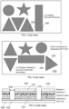
- the patterned display including encapsulated electrophoretic media is formed from a double release laminate 100 of the type described in U.S. Patent No. 7,561,324 .
- a double release laminate 100 of the type described in U.S. Patent No. 7,561,324 .
- FIG. 1 Such a construction is depicted in FIG. 1 , showing a first release sheet 110, a first adhesive layer 115, a second release sheet 120, and a second adhesive layer 125. Between the first release sheet 110 and the first adhesive layer 115, and the second release sheet 120 and the second adhesive layer 125, a layer of encapsulated electrophoretic media 130 is disposed.
- the layer of encapsulated electrophoretic media 130 maybe of any of the type discussed above, and may comprise a first type of electrophoretic particle 142 and a second type of electrophoretic particle 145 disposed in a non-polar solvent 147. Additionally, it is understood that an electrophoretic medium may include one, two, three, four, five, or six charged particles that move toward or away from the electrodes in the presence of an applied electric field.
- the electrophoretic medium is of a shuttering type in that it has a first mode where the pigment is distributed through the container (e.g., a microcapsule or microcell), which creates a darkened state, and a second mode where the pigment is collected in a smaller volume to reduce the amount of transmissive light absorbed, thereby providing a light-transmissive medium.
- the container e.g., a microcapsule or microcell
- the pigment is collected in a smaller volume to reduce the amount of transmissive light absorbed, thereby providing a light-transmissive medium.
- a mixture of patterned electro-optic materials such as black and white switching media in a first portion of encapsulated electrophoretic media and blue and white switching media in a second portion of encapsulated electrophoretic media.
- the patterned capsules or partitioned microcells may be additionally colored, e.g., with ink jet printing before an additional conductive layer is adhered to the capsules.
- the different portions of encapsulated electrophoretic media include the same types of electrophoretic particles. In some embodiments, the different portions of encapsulated electrophoretic media include different types of electrophoretic particles.
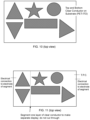
- the double release laminate 100 can be patterned to create a first portion of encapsulated electrophoretic media 220 and a second portion of encapsulated electrophoretic media 240, as shown in FIG. 2 .
- the patterning can be done with, for example a laser, scissors, a knife, or a die, represented by narrow wedges in FIG. 2 .
- the patterning may be all the way through the double release laminate 100, as shown in FIG. 2 , or the patterning may be only partially through the double release laminate 100, which allows the second release sheet 120 and the second adhesive layer 125 to remain intact.
- Such precision cutting is best achieved with a laser cutting assembly using a wavelength that is absorbed by a pigment of the electrophoretic medium.
- Such a laser cutting system may include, for example a Nd:YAG laser operating at the fundamental wavelength in the near-IR.
- a laser cutting system is available from Trotec Laser, Inc. (Plymouth, Michigan).
- a variety of portions of encapsulated electrophoretic media can be cut from a single sheet of double release laminate 100.
- One or more portions of remnant 250 may be removed from the double release laminate 100 to isolate the first portion of encapsulated electrophoretic media 220 and the second portion of encapsulated electrophoretic media 240 (and others, as appropriate) as shown in FIG. 4 .
- the double release laminate 100 is cut all of the way through both release layers, the resulting portions of encapsulated electrophoretic media are essentially double-sided stickers.
- the second release sheet 120 of each isolated portion can be removed and that portion of encapsulated electrophoretic media can be affixed to, for example, a sheet of PET-ITO using the second adhesive layer 125.
- the PET-ITO base thus becomes the second contiguous light-transmissive electrode 310 and the second light-transmissive substrate 320 of the claimed display, as shown in FIGS. 5 and 6 .
- the first portion of encapsulated electrophoretic media 220 and the second portion of encapsulated electrophoretic media 240 do not contact, because they are separated by a gap, i.e., as shown in FIG. 6 .
- the gap between the first portion of encapsulated electrophoretic media 220 and the second portion of encapsulated electrophoretic media 240 is typically at least 5mm, as measured parallel to the first contiguous light-transmissive electrode and the second contiguous light-transmissive electrode. In some instances, the gap is larger, e.g., at least 1 cm, e.g., at least 5 cm, e.g., between 1 cm and 10 cm.
- the first release sheet 110 can then be removed from all of the portions of encapsulated electrophoretic media, as shown in FIG. 7 .
- the first contiguous light-transmissive electrode 340 and the first light-transmissive substrate 350 are coated with a light-transmissive semi-conductive adhesive 360 and the assembly of the first contiguous light-transmissive electrode 340, the first light-transmissive substrate 350, and the light-transmissive semi-conductive adhesive 360 are applied to the collection of the first portion of encapsulated electrophoretic media 220, the second portion of encapsulated electrophoretic media 240, the second contiguous light-transmissive electrode 310, and the second light-transmissive substrate 320 as shown in FIG. 8 .
- the resulting electrophoretic display is shown in a side profile in FIG. 9 , and from above in FIG. 10 .
- the light-transmissive semi-conductive adhesive 360 can be made from a number of different light-transmissive adhesives such as acrylics and polyurethanes, however polyurethanes are typically preferred. It is important that the light-transmissive semi-conductive adhesive 360 is sufficiently conductive that it does not create a dielectric layer between the first contiguous light-transmissive electrode 340 and the layers of electrophoretic media, however it must not be conductive enough to create a shorting pathway between the first contiguous light-transmissive electrode 340 and the second contiguous light-transmissive electrode 310, especially in the gap between the first portion of encapsulated electrophoretic media 220 and the second portion of encapsulated electrophoretic media 240.
- light-transmissive semi-conductive adhesive 360 is sufficiently conductive that it does not create a dielectric layer between the first contiguous light-transmissive electrode 340 and the layers of electrophoretic media, however it must not be conductive enough to create a shorting pathway between the first contiguous light-transmissive
- the light-transmissive semi-conductive adhesive 360 is typically doped with a salt or charged polymers.
- the salt may be, for example, an inorganic salt, an organic salt, or a combination thereof.
- the salt comprises potassium acetate.
- the salt may comprise a quaternary ammonium salt, for example a tetraalkylammonium salt, such as tetrabutylammonium chloride or hexafluorophosphate.
- Suitable light-transmissive semi-conductive adhesive 360 are available from Merck KGaA.
- the volume resistivity of the light-transmissive semi-conductive adhesive 360 is typically between 1 x 10 5 and 1 x 10 12 Ohm cm.
- the invention is not limited to the embodiment shown in FIGS. 9 and 10 .
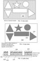
- the final assembly of the first portion of encapsulated electrophoretic media 220 and the second portion of encapsulated electrophoretic media 240 disposed between the first contiguous light-transmissive electrode 340 and the second contiguous light-transmissive electrode 310 can be made to switch optical states separately, as shown in FIG. 11 .
- Using a different type of laser, or a knife it is possible to cut through only one of the two contiguous light-transmissive electrodes, thereby dividing the display into zones that can be separately controlled with different power connections.
- an assembly comprising, for example, eight different zones of switching, each with multiple portions of encapsulated electrophoretic media can be created.
- Alternate methods of fabricating a display of the invention include using a mask, template, or stencil 410 as shown in FIG. 12 .
- the starting substrate is the second contiguous light-transmissive electrode 310 on the second light-transmissive substrate 320, however the stencil 410 is placed atop the light-transmissive electrode 310 and a layer of encapsulated electrophoretic media 130 is applied over the entire stencil, e.g., using a bar coating method or spray coating the electrophoretic media.
- the first portion of encapsulated electrophoretic media 220 and the second portion of encapsulated electrophoretic media 240 remain on the second contiguous light-transmissive electrode 310 on the second light-transmissive substrate 320, very similar to the structure shown in FIG. 5 , however the structure of FIG. 13 is missing the first release sheet 110 and the first adhesive layer 115. Compare FIGS. 5 and 6 to FIGS. 13 and 14 . It is noted that this alternative method of creating the electrophoretic display only works with encapsulated electrophoretic media that are encapsulated in microcapsules which can be coated over the stencil as a slurry or sprayed with a spray gun (see U.S. Patent No. 9,835,925 ).
- the alternative method is completed with the addition of the first contiguous light-transmissive electrode 340 and the first light-transmissive substrate 350 that have been coated with a light-transmissive semi-conductive adhesive 360 the first portion of encapsulated electrophoretic media 220, the second portion of encapsulated electrophoretic media 240, the second contiguous light-transmissive electrode 310, and the second light-transmissive substrate 320.
- FIG. 8 and FIG. 15 The final structure, FIG. 14 is very similar to the final structure using the first method, however the first adhesive layer 115 is missing from FIG. 16 . Compare FIG. 9 and FIG. 16 .
- removing a layer of adhesive is optically-beneficial because every layer of differential materials presents a new scattering interface.
- the design of FIG. 16 may have lower haze and better transmission when the electrophoretic media is of the shuttering type.
- the electrophoretic material layer of the present invention may comprises an electrophoretic medium.
- the electrophoretic medium may be compartmentalized in microcapsules or in microcell.
- the electrophoretic material layers has an upper surface, a lower surface, and a peripheral surface. The upper surface and the lower surface are on opposite sides of the electrophoretic material layer.
- the upper surface of the electrophoretic material layer is defined by a perimeter. The perimeter has a length and a width.
- the electro-optic device of the present invention may comprise a first adhesive layer and/or a second adhesive layer.
- the first adhesive layer has an upper surface, a lower surface, and a peripheral surface.
- the adhesives can be made from a variety of materials, such as acrylics and polyurethanes, however polyurethanes are typically preferred.
- the upper surface and the lower surface are on opposite sides of the first adhesive layer.
- the term "length and width of the first adhesive layer” refers to the length width dimensions of the upper surface of the first adhesive layer.
- the second adhesive layer has an upper surface, a lower surface, and a peripheral surface. The upper surface and the lower surface are on opposite sides of the second adhesive layer.
- the term "length and width of the second adhesive layer” refers to the length and width dimensions of the upper surface of the second adhesive layer.
- the electro-optic device of the present invention comprises a backplane, which may be used interchangeable with a second electrode layer.
- the backplane has an upper surface, a lower surface, and a peripheral surface. The upper surface and the lower surface are on opposite sides of the backplane.
- the term "length and width of the backplane" refers to the length and width of the upper surface of the backplane.
- active display area is the area of the viewing surface of the electrophoretic display where a variable image can be displayed.
- Variable image of an electrophoretic display is an image that can be created as a result of the application of electric field on an electrophoretic material layer of the electrophoretic display.
- the electro-optic material is an electrophoretic medium compartmentalized in microcapsules.
- the electrophoretic medium may be compartmentalized in microcells.
- the electrophoretic medium may comprise electrophoretic particles in a non-polar liquid.
- an encapsulated electrophoretic medium comprising microcapsules in a binder is coated onto a flexible substrate comprising indium-in-oxide (ITO) or similar conductive coating or an adhesive coupled to a release sheet, i.e., as described above.
- the conductive coating is the first light-transmissive electrode layer. Drying or curing the microcapsules/binder coating forms the electro-optic material layer, which is firmly adhered to the first light-transmissive layer.
- Microcapsules suitable for use with the invention may include gelatin-acacia microcapsules as described in U.S.
- Patents 7,230,750 and 10,983,410 include non-ionic polymers, such as polyvinyl alcohol, as described in U.S. Patent Publication No. 2021/0191226 .
- the binder is typically cured with heat or UV light, and may be cross-linked as needed for the application.
- Binders suitable for use with encapsulated electrophoretic media include polyurethanes, such as sold by Merck KGaA, and acrylics such as sold by Sartomer (a division of Arkema). More examples of suitable binders can be found in U.S. Patent No. 9,777,201 .
- the encapsulated electrophoretic media is encapsulated in a plurality of microcells.
- the microcells may be square, round, or polygonal, such as a honeycomb structure.
- the microcells are typically fabricated by microembossing sheets of acrylic or methacrylic sheet materials, as described in U.S. Patent No. 6,930,818 .
- Each microcell includes an opening that is spanned by a polymeric sealing layer.
- the polymeric sealing layer may be constructed from a variety of materials, such acrylate, methacrylate, polycarbonate, polyvinyl alcohol, cellulose, poly(N-isopropylacrylamide) (PNIPAAm), poly(lactic-co-glycolic acid) (PLGA), polyethylene, polypropylene, or polystyrene.
- PNIPAAm poly(N-isopropylacrylamide)
- PLGA poly(lactic-co-glycolic acid)
- the encapsulated electrophoretic media in microcells may be prepared as a double release laminate, or the microcells can be coupled to a light-transmissive electrode layer on a light-transmissive substrate, such as PET-ITO.
- the light-transmissive top (or bottom) conductive layer (electrode) may be carried on a light-transmissive substrate, which is preferably flexible, in the sense that the substrate can be manually wrapped around a drum, say, 25 mm in diameter without permanent deformation.
- the substrate will be typically a polymeric film, and will normally have a thickness in the range of about 1 to about 25 mil (25 to 634 ⁇ m), preferably about 2 to about 10 mil (51 to 254 ⁇ m).
- the light-transmissive electrode is conveniently a thin metal layer of, for example, aluminum or indium-tin-oxide (ITO), or may be a conductive polymer.
- PET films coated with aluminum or ITO are available commercially, for example as "aluminized Mylar” ("Mylar” is a Registered Trade Mark) from E.I. du Pont de Nemours & Company, Wilmington Del., and such commercial materials may be used with good results in the front plane laminate.
- a light-transmissive substrate need not be flexible, however.
- a light-transmissive substrate may be, for example, glass or a clear rigid polymer, such as cross-linked acrylic or another rigid light-transmissive polymer.
- Assembly of an electro-optic device using such a front plane laminate may be ffected by removing the release sheet from the front plane laminate and contacting the first adhesive layer with the backplane under conditions effective to cause the first adhesive layer to adhere to the backplane, thereby securing the first adhesive layer, electrophoretic medium and electrically-conductive layer to the backplane.
- This process is well-adapted to mass production since the front plane laminate may be mass produced, typically using roll-to-roll coating techniques, and then cut into pieces of any size needed for use with specific backplanes.
- an edge seal compositions is dispensed around the piece to create the conductive edge seal after drying or curing of the edge seal composition.
- the device is typically exposed to a moisture conditioning step at certain temperature and relative humidity before edge sealing.
- a patterned display including encapsulated electrophoretic media may additionally include an edge seal.
- the edge seal composition may comprise a polymer or combination of polymers. Drying or curing of the edge seal composition forms the edge seal of the device.
- Non-limiting examples of polymers are polyurethane, epoxy, polydimethylsiloxane, polyacrylate, polymethacrylate, polycarbonate, polyvinyl chloride, polystyrene-alkylene copolymer, polyamide, polyester, polystyrene, polyethylene, polypropylene, polyisobutylene, poly(ethylene terephthalate), poly(ethylene naphthalate), ethylene-vinyl alcohol copolymer, poly(ethylene-co-norbornene), styrene-isobutylene-styrene block copolymer and mixtures thereof.
- the edge seal composition may comprise conductive fillers such as metal particles, metal nanoparticles, metal wires, metal nanowires, metal nanofibers, conductive carbon black particles, carbon nanotubes, graphite, and combinations thereof.
- the edge seal composition may also comprise conductive polymers.
- Non-limiting examples of conductive polymers are poly(3,4-ethylenedioxythiophene) polystyrene sulfonate (PEDOT-PSS), polyacetylene, polyphenylene sulfide, polyphenylene vinylene, and combinations thereof.
- a display of the invention may additionally include a barrier layer 3140, as shown in FIG.
- the barrier layer may also protect against physical damage due to, e.g., contact with a sharp object.
- Suitable barrier materials include polyethylenes, polyimides, glass, and vapor deposited ceramics, such as indium tin oxide and silicon nitride.
- An additional layer of optically-clear adhesive (OCA) may be used to adhere the barrier layer 510 to the first light-transmissive substrate 350.
Landscapes
- Physics & Mathematics (AREA)
- Nonlinear Science (AREA)
- General Physics & Mathematics (AREA)
- Optics & Photonics (AREA)
- Health & Medical Sciences (AREA)
- Life Sciences & Earth Sciences (AREA)
- Chemical & Material Sciences (AREA)
- Chemical Kinetics & Catalysis (AREA)
- Electrochemistry (AREA)
- Molecular Biology (AREA)
- Electrochromic Elements, Electrophoresis, Or Variable Reflection Or Absorption Elements (AREA)
Claims (15)
- Elektrophoretische Anzeige, umfassend:eine erste zusammenhängende lichtdurchlässige Elektrode (340), die auf einem ersten lichtdurchlässigen Substrat (350) angeordnet ist;eine zweite zusammenhängende lichtdurchlässige Elektrode (310), die auf einem zweiten lichtdurchlässigen Substrat (320) angeordnet ist;einen ersten Teil verkapselter elektrophoretischer Medien (220), der zwischen der ersten zusammenhängenden lichtdurchlässigen Elektrode (350) und der zweiten zusammenhängenden lichtdurchlässigen Elektrode (310) angeordnet ist;einen zweiten Teil verkapselter elektrophoretischer Medien (240), der zwischen der ersten zusammenhängenden lichtdurchlässigen Elektrode und der zweiten zusammenhängenden lichtdurchlässigen Elektrode angeordnet ist; undeinen lichtdurchlässigen halbleitenden Klebstoff (360), der zwischen der ersten zusammenhängenden lichtdurchlässigen Elektrode und der zweiten zusammenhängenden lichtdurchlässigen Elektrode angeordnet ist, wobei der halbleitende Klebstoff (360) einen Volumenwiderstand zwischen 1 x 10⁵ und 1 x 10¹² Ohm·cm aufweist,wobei der lichtdurchlässige halbleitende Klebstoff zwischen der ersten zusammenhängenden lichtdurchlässigen Elektrode und dem ersten Teil verkapselter elektrophoretischer Medien und zwischen der ersten zusammenhängenden lichtdurchlässigen Elektrode und dem zweiten Teil verkapselter elektrophoretischer Medien angeordnet ist,wobei der erste Teil verkapselter elektrophoretischer Medien (220) den zweiten Teil verkapselter elektrophoretischer Medien (240) nicht berührt und der lichtdurchlässige halbleitende Klebstoff (360) den ersten Teil des verkapselter elektrophoretischer Medien (220) und den zweiten Teil verkapselter elektrophoretischer Medien (240) trennt,wobei sich die erste zusammenhängende lichtdurchlässige Elektrode sowohl über den ersten Teil als auch den zweiten Teil verkapselter elektrophoretischer Medien erstreckt,wobei sich die zweite zusammenhängende lichtdurchlässige Elektrode sowohl über den ersten Teil als auch den zweiten Teil verkapselter elektrophoretischer Medien erstreckt, undwobei das Anlegen eines elektrischen Feldes zwischen der ersten zusammenhängenden lichtdurchlässigen Elektrode und der zweiten zusammenhängenden lichtdurchlässigen Elektrode (310) eine Änderung des optischen Zustands sowohl des ersten Teils verkapselter elektrophoretischer Medien (220) als auch des zweiten Teils verkapselter elektrophoretischer Medien (240) bewirkt.
- Elektrophoretische Anzeige nach Anspruch 1, wobei der erste Teil verkapselter elektrophoretischer Medien (220) einen ersten Typ elektrophoretischer Partikel (142) umfasst und der zweite Teil verkapselter elektrophoretischer Medien (240) den ersten Typ elektrophoretischer Partikel (142) umfasst.
- Elektrophoretische Anzeige nach Anspruch 1, wobei der erste Teil verkapselter elektrophoretischer Medien (220) einen ersten Typ elektrophoretischer Partikel (142) umfasst und der zweite Teil verkapselter elektrophoretischer Medien (240) einen zweiten Typ elektrophoretischer Partikel (145) umfasst und der erste und der zweite Typ elektrophoretischer Partikel (142, 145) unterschiedliche optische Eigenschaften aufweisen.
- Elektrophoretische Anzeige nach einem der Ansprüche 1-3, wobei der erste Teil verkapselter elektrophoretischer Medien (220) und der zweite Teil verkapselter elektrophoretischer Medien (240) beide mehr als einen Typ elektrophoretischer Partikel (142, 145) umfassen.
- Elektrophoretische Anzeige nach Anspruch 1, wobei der erste Teil verkapselter elektrophoretischer Medien (220) in Mikrokapseln verkapselt ist und die Mikrokapseln mit einem polymeren Bindemittel zusammengehalten werden.
- Elektrophoretische Anzeige nach Anspruch 5, wobei die Mikrokapseln Gelatine oder Polyvinylalkohol umfassen.
- Elektrophoretische Anzeige nach Anspruch 6, wobei das polymere Bindemittel ein Polyurethan oder ein Acrylat umfasst.
- Elektrophoretische Anzeige nach Anspruch 1, wobei der lichtdurchlässige halbleitende Klebstoff (360) mit einem anorganischen Salz dotiertes Polyurethan umfasst.
- Elektrophoretische Anzeige nach Anspruch 8, wobei der lichtdurchlässige halbleitende Klebstoff (360) Polyurethan umfasst, das mit einem anorganischen Salz in einer Konzentration zwischen 2 Gew.-% und 0,05 Gew.-% dotiert ist.
- Elektrophoretische Anzeige nach Anspruch 1, wobei der erste Teil verkapselter elektrophoretischer Medien (220) und der zweite Teil verkapselter elektrophoretischer Medien (240) durch einen Abstand von mindestens 5 mm getrennt sind, wie parallel zu der ersten zusammenhängenden lichtdurchlässigen Elektrode und der zweiten zusammenhängenden lichtdurchlässigen Elektrode gemessen.
- Verfahren zur Herstellung einer elektrophoretischen Anzeige, umfassend:Bereitstellen einer Schicht verkapselter elektrophoretischer Medien (130), die zwischen einer ersten Trennfolie (110) und einer ersten Klebstoffschicht (115) und einer zweiten Trennfolie (120) und einer zweiten Klebstoffschicht (125) angeordnet wird;Strukturieren der Schicht verkapselter elektrophoretischer Medien (130) durch Durchschneiden der ersten Trennfolie (110), der ersten Klebstoffschicht (115) und der Schicht verkapselter elektrophoretischer Medien (130), um einen ersten Teil verkapselter elektrophoretischer Medien (220) und einen zweiten Teil verkapselter elektrophoretischer Medien (240) zu erzeugen;Anordnen des ersten Teils verkapselter elektrophoretischer Medien (220) und des zweiten Teils verkapselter elektrophoretischer Medien (240) zwischen einer ersten zusammenhängenden lichtdurchlässigen Elektrode (340), die auf einem ersten lichtdurchlässigen Substrat (350) angeordnet ist, und einer zweiten zusammenhängenden lichtdurchlässigen Elektrode (310), die auf einem zweiten lichtdurchlässigen Substrat (320) angeordnet ist, so dass der erste Teil elektrophoretischer Medien (220) den zweiten Teil elektrophoretischer Medien (240) nicht berührt, wobei sich die erste zusammenhängende lichtdurchlässige Elektrode sowohl über den ersten Teil als auch den zweiten Teil verkapselter elektrophoretischer Medien erstreckt, wobei sich die zweite zusammenhängende lichtdurchlässige Elektrode sowohl über den ersten Teil als auch den zweiten Teil verkapselter elektrophoretischer Medien erstreckt,wobei ein lichtdurchlässiger halbleitender Klebstoff (360) zwischen der ersten zusammenhängenden lichtdurchlässigen Elektrode (340) und der zweiten zusammenhängenden lichtdurchlässigen Elektrode (310) angeordnet wird, wobei der lichtdurchlässige halbleitende Klebstoff (360) den ersten Teil verkapselter elektrophoretischer Medien (220) von dem zweiten Teil verkapselter elektrophoretischer Medien (240) trennt, wobei der halbleitende Klebstoff (360) einen Volumenwiderstand zwischen 1 x 10⁵ und 1 x 10¹² Ohm·cm aufweist, wobei der lichtdurchlässige halbleitende Klebstoff zwischen der ersten zusammenhängenden lichtdurchlässigen Elektrode und dem ersten Teil verkapselter elektrophoretischer Medien und zwischen der ersten zusammenhängenden lichtdurchlässigen Elektrode und dem zweiten Teil verkapselter elektrophoretischer Medien angeordnet wird.
- Verfahren nach Anspruch 11, wobei der erste Teil verkapselter elektrophoretischer Medien (220) und der zweite Teil verkapselter elektrophoretischer Medien (240) durch einen Abstand von mindestens 5 mm getrennt sind, wie parallel zu der ersten zusammenhängenden lichtdurchlässigen Elektrode (340) und der zweiten zusammenhängenden lichtdurchlässigen Elektrode (310) gemessen.
- Verfahren nach Anspruch 11, wobei das Strukturieren Durchschneiden der zweiten Trennfolie (120) und der zweiten Klebstoffschicht (125) umfasst.
- Verfahren nach Anspruch 11 oder 13, wobei das Strukturieren mit einem Laser, einer Schere, einem Messer oder einem Schneidwerkzeug erfolgt.
- Verfahren nach Anspruch 11, wobei der Strukturierungsschritt ferner Erzeugen eines Restteils verkapselter elektrophoretischer Medien (250) umfasst und das Verfahren ferner Entfernen des Restteils (250) verkapselter elektrophoretischer Medien aus der Schicht verkapselter elektrophoretischer Medien (130) umfasst.
Applications Claiming Priority (2)
| Application Number | Priority Date | Filing Date | Title |
|---|---|---|---|
| US202263330751P | 2022-04-13 | 2022-04-13 | |
| PCT/US2023/018318 WO2023200859A1 (en) | 2022-04-13 | 2023-04-12 | Display material including patterned areas of encapsulated electrophoretic media |
Publications (3)
| Publication Number | Publication Date |
|---|---|
| EP4476591A1 EP4476591A1 (de) | 2024-12-18 |
| EP4476591B1 true EP4476591B1 (de) | 2025-06-11 |
| EP4476591C0 EP4476591C0 (de) | 2025-06-11 |
Family
ID=86328310
Family Applications (1)
| Application Number | Title | Priority Date | Filing Date |
|---|---|---|---|
| EP23721537.1A Active EP4476591B1 (de) | 2022-04-13 | 2023-04-12 | Anzeigematerial mit strukturierten bereichen verkapselter elektrophoretischer medien |
Country Status (9)
| Country | Link |
|---|---|
| US (1) | US20230333437A1 (de) |
| EP (1) | EP4476591B1 (de) |
| JP (1) | JP2025511995A (de) |
| KR (1) | KR20240155329A (de) |
| CN (1) | CN118871854A (de) |
| ES (1) | ES3035946T3 (de) |
| PL (1) | PL4476591T3 (de) |
| TW (2) | TWI877082B (de) |
| WO (1) | WO2023200859A1 (de) |
Family Cites Families (69)
| Publication number | Priority date | Publication date | Assignee | Title |
|---|---|---|---|---|
| US6137467A (en) | 1995-01-03 | 2000-10-24 | Xerox Corporation | Optically sensitive electric paper |
| US6866760B2 (en) | 1998-08-27 | 2005-03-15 | E Ink Corporation | Electrophoretic medium and process for the production thereof |
| US7411719B2 (en) | 1995-07-20 | 2008-08-12 | E Ink Corporation | Electrophoretic medium and process for the production thereof |
| US5760761A (en) | 1995-12-15 | 1998-06-02 | Xerox Corporation | Highlight color twisting ball display |
| US6055091A (en) | 1996-06-27 | 2000-04-25 | Xerox Corporation | Twisting-cylinder display |
| US5808783A (en) | 1996-06-27 | 1998-09-15 | Xerox Corporation | High reflectance gyricon display |
| US5777782A (en) | 1996-12-24 | 1998-07-07 | Xerox Corporation | Auxiliary optics for a twisting ball display |
| US7002728B2 (en) | 1997-08-28 | 2006-02-21 | E Ink Corporation | Electrophoretic particles, and processes for the production thereof |
| US6054071A (en) | 1998-01-28 | 2000-04-25 | Xerox Corporation | Poled electrets for gyricon-based electric-paper displays |
| US7075502B1 (en) | 1998-04-10 | 2006-07-11 | E Ink Corporation | Full color reflective display with multichromatic sub-pixels |
| US6241921B1 (en) | 1998-05-15 | 2001-06-05 | Massachusetts Institute Of Technology | Heterogeneous display elements and methods for their fabrication |
| US6128124A (en) | 1998-10-16 | 2000-10-03 | Xerox Corporation | Additive color electric paper without registration or alignment of individual elements |
| US6147791A (en) | 1998-11-25 | 2000-11-14 | Xerox Corporation | Gyricon displays utilizing rotating elements and magnetic latching |
| US6097531A (en) | 1998-11-25 | 2000-08-01 | Xerox Corporation | Method of making uniformly magnetized elements for a gyricon display |
| US7012600B2 (en) | 1999-04-30 | 2006-03-14 | E Ink Corporation | Methods for driving bistable electro-optic displays, and apparatus for use therein |
| US8009348B2 (en) | 1999-05-03 | 2011-08-30 | E Ink Corporation | Machine-readable displays |
| US6930818B1 (en) | 2000-03-03 | 2005-08-16 | Sipix Imaging, Inc. | Electrophoretic display and novel process for its manufacture |
| US6672921B1 (en) | 2000-03-03 | 2004-01-06 | Sipix Imaging, Inc. | Manufacturing process for electrophoretic display |
| US6788449B2 (en) | 2000-03-03 | 2004-09-07 | Sipix Imaging, Inc. | Electrophoretic display and novel process for its manufacture |
| US7715088B2 (en) | 2000-03-03 | 2010-05-11 | Sipix Imaging, Inc. | Electrophoretic display |
| WO2002073572A2 (en) | 2001-03-13 | 2002-09-19 | E Ink Corporation | Apparatus for displaying drawings |
| US7679814B2 (en) | 2001-04-02 | 2010-03-16 | E Ink Corporation | Materials for use in electrophoretic displays |
| US7230750B2 (en) | 2001-05-15 | 2007-06-12 | E Ink Corporation | Electrophoretic media and processes for the production thereof |
| DE60210949T2 (de) | 2001-04-02 | 2006-09-21 | E-Ink Corp., Cambridge | Elektrophoresemedium mit verbesserter Bildstabilität |
| US20020188053A1 (en) | 2001-06-04 | 2002-12-12 | Sipix Imaging, Inc. | Composition and process for the sealing of microcups in roll-to-roll display manufacturing |
| US7561324B2 (en) * | 2002-09-03 | 2009-07-14 | E Ink Corporation | Electro-optic displays |
| US6982178B2 (en) | 2002-06-10 | 2006-01-03 | E Ink Corporation | Components and methods for use in electro-optic displays |
| US7535624B2 (en) | 2001-07-09 | 2009-05-19 | E Ink Corporation | Electro-optic display and materials for use therein |
| EP1429178A4 (de) | 2001-09-19 | 2005-11-02 | Bridgestone Corp | Partikel und einrichtung zur bildanzeige |
| EP2363745A1 (de) | 2001-12-10 | 2011-09-07 | Bridgestone Corporation | Bildanzeige |
| EP1484635A4 (de) | 2002-02-15 | 2008-02-20 | Bridgestone Corp | Bildanzeigeeinheit |
| AU2003213409A1 (en) | 2002-03-06 | 2003-09-16 | Bridgestone Corporation | Image displaying apparatus and method |
| AU2003235217A1 (en) | 2002-04-17 | 2003-10-27 | Bridgestone Corporation | Image display unit |
| US7116318B2 (en) | 2002-04-24 | 2006-10-03 | E Ink Corporation | Backplanes for display applications, and components for use therein |
| EP1500971B1 (de) | 2002-04-26 | 2010-01-13 | Bridgestone Corporation | Methode zur Herstellung eines sphärischen Partikels zur Bildanzeige |
| US7649674B2 (en) | 2002-06-10 | 2010-01-19 | E Ink Corporation | Electro-optic display with edge seal |
| KR100729970B1 (ko) | 2002-06-21 | 2007-06-20 | 가부시키가이샤 브리지스톤 | 화상 표시 장치 및 화상 표시 장치의 제조 방법 |
| AU2003252656A1 (en) | 2002-07-17 | 2004-02-02 | Bridgestone Corporation | Image display |
| US7839564B2 (en) | 2002-09-03 | 2010-11-23 | E Ink Corporation | Components and methods for use in electro-optic displays |
| TWI229230B (en) | 2002-10-31 | 2005-03-11 | Sipix Imaging Inc | An improved electrophoretic display and novel process for its manufacture |
| US7495819B2 (en) | 2002-12-17 | 2009-02-24 | Bridgestone Corporation | Method of manufacturing image display panel, method of manufacturing image display device, and image display device |
| US6922276B2 (en) | 2002-12-23 | 2005-07-26 | E Ink Corporation | Flexible electro-optic displays |
| EP1577702A4 (de) | 2002-12-24 | 2006-09-27 | Bridgestone Corp | Bildanzeige |
| TWI337679B (en) | 2003-02-04 | 2011-02-21 | Sipix Imaging Inc | Novel compositions and assembly process for liquid crystal display |
| WO2004077140A1 (ja) | 2003-02-25 | 2004-09-10 | Bridgestone Corporation | 画像表示用パネル及び画像表示装置 |
| JPWO2004079442A1 (ja) | 2003-03-06 | 2006-06-08 | 株式会社ブリヂストン | 画像表示装置の製造方法及び画像表示装置 |
| JP2004271724A (ja) * | 2003-03-06 | 2004-09-30 | Seiko Epson Corp | マイクロカプセル型電気泳動表示体およびその製造方法、マイクロカプセルの配置装置 |
| US7236291B2 (en) | 2003-04-02 | 2007-06-26 | Bridgestone Corporation | Particle use for image display media, image display panel using the particles, and image display device |
| US7075703B2 (en) | 2004-01-16 | 2006-07-11 | E Ink Corporation | Process for sealing electro-optic displays |
| US7453445B2 (en) | 2004-08-13 | 2008-11-18 | E Ink Corproation | Methods for driving electro-optic displays |
| WO2007002452A2 (en) | 2005-06-23 | 2007-01-04 | E Ink Corporation | Edge seals and processes for electro-optic displays |
| US7733554B2 (en) | 2006-03-08 | 2010-06-08 | E Ink Corporation | Electro-optic displays, and materials and methods for production thereof |
| US8610988B2 (en) | 2006-03-09 | 2013-12-17 | E Ink Corporation | Electro-optic display with edge seal |
| US20150005720A1 (en) | 2006-07-18 | 2015-01-01 | E Ink California, Llc | Electrophoretic display |
| US8034209B2 (en) | 2007-06-29 | 2011-10-11 | E Ink Corporation | Electro-optic displays, and materials and methods for production thereof |
| JP2011065033A (ja) * | 2009-09-18 | 2011-03-31 | Toppan Printing Co Ltd | 多面付けカラーフィルタ電気泳動方式前面板及びその製造方法、並びに、多色表示パネルの製造方法 |
| KR101738452B1 (ko) * | 2009-10-20 | 2017-06-08 | 엘지디스플레이 주식회사 | 전기영동 표시소자 및 그 제조방법 |
| TWI457679B (zh) * | 2011-06-03 | 2014-10-21 | E Ink Holdings Inc | 電泳顯示器 |
| US9279906B2 (en) | 2012-08-31 | 2016-03-08 | E Ink California, Llc | Microstructure film |
| JP2014170110A (ja) * | 2013-03-04 | 2014-09-18 | Seiko Epson Corp | 制御装置、電気光学装置、電子機器および制御方法 |
| WO2015089663A1 (en) * | 2013-12-19 | 2015-06-25 | Switch Materials Inc. | Switchable objects and methods of manufacture |
| US10444553B2 (en) | 2014-03-25 | 2019-10-15 | E Ink California, Llc | Magnetophoretic display assembly and driving scheme |
| TWI559915B (en) | 2014-07-10 | 2016-12-01 | Sipix Technology Inc | Smart medication device |
| US9835925B1 (en) | 2015-01-08 | 2017-12-05 | E Ink Corporation | Electro-optic displays, and processes for the production thereof |
| CN112859476B (zh) | 2015-07-23 | 2024-06-14 | 伊英克公司 | 用于电光介质的聚合物制剂 |
| CN110603484B (zh) | 2017-06-16 | 2023-05-02 | 伊英克公司 | 包含在明胶粘结剂中的胶囊化颜料的电光介质 |
| CN109613784A (zh) * | 2019-01-24 | 2019-04-12 | 中山大学 | 可拉伸电子纸、一体化电子纸装饰品及相应的制作方法 |
| JP7464718B2 (ja) | 2019-12-23 | 2024-04-09 | イー インク コーポレイション | 非イオン性ポリマー壁を伴うマイクロカプセルを含むカラー電気泳動層 |
| KR20220024328A (ko) * | 2022-02-09 | 2022-03-03 | 주식회사 나노브릭 | 전기 투과도 가변 필름 및 그 제조 방법 |
-
2023
- 2023-04-12 EP EP23721537.1A patent/EP4476591B1/de active Active
- 2023-04-12 US US18/133,794 patent/US20230333437A1/en active Pending
- 2023-04-12 PL PL23721537.1T patent/PL4476591T3/pl unknown
- 2023-04-12 WO PCT/US2023/018318 patent/WO2023200859A1/en not_active Ceased
- 2023-04-12 KR KR1020247032805A patent/KR20240155329A/ko active Pending
- 2023-04-12 ES ES23721537T patent/ES3035946T3/es active Active
- 2023-04-12 CN CN202380026051.9A patent/CN118871854A/zh active Pending
- 2023-04-12 JP JP2024559894A patent/JP2025511995A/ja active Pending
- 2023-04-13 TW TW113136657A patent/TWI877082B/zh active
- 2023-04-13 TW TW112113847A patent/TWI857562B/zh active
Also Published As
| Publication number | Publication date |
|---|---|
| WO2023200859A1 (en) | 2023-10-19 |
| TWI877082B (zh) | 2025-03-11 |
| CN118871854A (zh) | 2024-10-29 |
| TWI857562B (zh) | 2024-10-01 |
| KR20240155329A (ko) | 2024-10-28 |
| EP4476591A1 (de) | 2024-12-18 |
| PL4476591T3 (pl) | 2025-10-06 |
| EP4476591C0 (de) | 2025-06-11 |
| US20230333437A1 (en) | 2023-10-19 |
| TW202407447A (zh) | 2024-02-16 |
| ES3035946T3 (en) | 2025-09-11 |
| TW202509605A (zh) | 2025-03-01 |
| JP2025511995A (ja) | 2025-04-16 |
Similar Documents
| Publication | Publication Date | Title |
|---|---|---|
| US12038666B2 (en) | Method of forming a top plane connection in an electro-optic device | |
| EP1719108B1 (de) | Elektrooptische anzeige mit auf das rücksubstrat aufgeklebter elektrooptischer schicht | |
| EP2309304B1 (de) | Verfahren zur Herstellung von elektrooptischen Anzeigen | |
| US9164207B2 (en) | Electro-optic media produced using ink jet printing | |
| EP3992706B1 (de) | Laminierte elektrooptische anzeigen und verfahren zur herstellung davon | |
| US12449706B2 (en) | Method of production of an electro-optic device comprising integrated conductive edge seal | |
| EP4476591B1 (de) | Anzeigematerial mit strukturierten bereichen verkapselter elektrophoretischer medien | |
| TWI774938B (zh) | 電光顯示器的組合體 | |
| EP4211513B1 (de) | Reflektierende mikrozellen für elektrophoretische anzeigen und verfahren zu ihrer herstellung | |
| HK40031048A (en) | Assemblies of electro-optic displays | |
| HK1098542B (en) | Process for sealing electro-optic display | |
| HK1098542A1 (zh) | 密封电光显示器的工艺过程 |
Legal Events
| Date | Code | Title | Description |
|---|---|---|---|
| STAA | Information on the status of an ep patent application or granted ep patent |
Free format text: STATUS: UNKNOWN |
|
| STAA | Information on the status of an ep patent application or granted ep patent |
Free format text: STATUS: THE INTERNATIONAL PUBLICATION HAS BEEN MADE |
|
| PUAI | Public reference made under article 153(3) epc to a published international application that has entered the european phase |
Free format text: ORIGINAL CODE: 0009012 |
|
| STAA | Information on the status of an ep patent application or granted ep patent |
Free format text: STATUS: REQUEST FOR EXAMINATION WAS MADE |
|
| 17P | Request for examination filed |
Effective date: 20240911 |
|
| AK | Designated contracting states |
Kind code of ref document: A1 Designated state(s): AL AT BE BG CH CY CZ DE DK EE ES FI FR GB GR HR HU IE IS IT LI LT LU LV MC ME MK MT NL NO PL PT RO RS SE SI SK SM TR |
|
| GRAP | Despatch of communication of intention to grant a patent |
Free format text: ORIGINAL CODE: EPIDOSNIGR1 |
|
| STAA | Information on the status of an ep patent application or granted ep patent |
Free format text: STATUS: GRANT OF PATENT IS INTENDED |
|
| GRAJ | Information related to disapproval of communication of intention to grant by the applicant or resumption of examination proceedings by the epo deleted |
Free format text: ORIGINAL CODE: EPIDOSDIGR1 |
|
| STAA | Information on the status of an ep patent application or granted ep patent |
Free format text: STATUS: REQUEST FOR EXAMINATION WAS MADE |
|
| GRAP | Despatch of communication of intention to grant a patent |
Free format text: ORIGINAL CODE: EPIDOSNIGR1 |
|
| STAA | Information on the status of an ep patent application or granted ep patent |
Free format text: STATUS: GRANT OF PATENT IS INTENDED |
|
| DAV | Request for validation of the european patent (deleted) | ||
| DAX | Request for extension of the european patent (deleted) | ||
| INTG | Intention to grant announced |
Effective date: 20250130 |
|
| INTC | Intention to grant announced (deleted) | ||
| INTG | Intention to grant announced |
Effective date: 20250227 |
|
| GRAS | Grant fee paid |
Free format text: ORIGINAL CODE: EPIDOSNIGR3 |
|
| GRAA | (expected) grant |
Free format text: ORIGINAL CODE: 0009210 |
|
| STAA | Information on the status of an ep patent application or granted ep patent |
Free format text: STATUS: THE PATENT HAS BEEN GRANTED |
|
| AK | Designated contracting states |
Kind code of ref document: B1 Designated state(s): AL AT BE BG CH CY CZ DE DK EE ES FI FR GB GR HR HU IE IS IT LI LT LU LV MC ME MK MT NL NO PL PT RO RS SE SI SK SM TR |
|
| REG | Reference to a national code |
Ref country code: GB Ref legal event code: FG4D |
|
| REG | Reference to a national code |
Ref country code: CH Ref legal event code: EP |
|
| REG | Reference to a national code |
Ref country code: IE Ref legal event code: FG4D |
|
| REG | Reference to a national code |
Ref country code: DE Ref legal event code: R096 Ref document number: 602023003984 Country of ref document: DE |
|
| U01 | Request for unitary effect filed |
Effective date: 20250623 |
|
| U07 | Unitary effect registered |
Designated state(s): AT BE BG DE DK EE FI FR IT LT LU LV MT NL PT RO SE SI Effective date: 20250627 |
|
| REG | Reference to a national code |
Ref country code: ES Ref legal event code: FG2A Ref document number: 3035946 Country of ref document: ES Kind code of ref document: T3 Effective date: 20250911 |
|
| PG25 | Lapsed in a contracting state [announced via postgrant information from national office to epo] |
Ref country code: GR Free format text: LAPSE BECAUSE OF FAILURE TO SUBMIT A TRANSLATION OF THE DESCRIPTION OR TO PAY THE FEE WITHIN THE PRESCRIBED TIME-LIMIT Effective date: 20250912 |
|
| PG25 | Lapsed in a contracting state [announced via postgrant information from national office to epo] |
Ref country code: HR Free format text: LAPSE BECAUSE OF FAILURE TO SUBMIT A TRANSLATION OF THE DESCRIPTION OR TO PAY THE FEE WITHIN THE PRESCRIBED TIME-LIMIT Effective date: 20250611 |
|
| PG25 | Lapsed in a contracting state [announced via postgrant information from national office to epo] |
Ref country code: RS Free format text: LAPSE BECAUSE OF FAILURE TO SUBMIT A TRANSLATION OF THE DESCRIPTION OR TO PAY THE FEE WITHIN THE PRESCRIBED TIME-LIMIT Effective date: 20250911 |