EP4474803A1 - Inspection device and inspection method - Google Patents
Inspection device and inspection method Download PDFInfo
- Publication number
- EP4474803A1 EP4474803A1 EP22924089.0A EP22924089A EP4474803A1 EP 4474803 A1 EP4474803 A1 EP 4474803A1 EP 22924089 A EP22924089 A EP 22924089A EP 4474803 A1 EP4474803 A1 EP 4474803A1
- Authority
- EP
- European Patent Office
- Prior art keywords
- inspection
- ray
- target surface
- foreign substance
- inspection target
- Prior art date
- Legal status (The legal status is an assumption and is not a legal conclusion. Google has not performed a legal analysis and makes no representation as to the accuracy of the status listed.)
- Pending
Links
Images





Classifications
-
- G—PHYSICS
- G01—MEASURING; TESTING
- G01N—INVESTIGATING OR ANALYSING MATERIALS BY DETERMINING THEIR CHEMICAL OR PHYSICAL PROPERTIES
- G01N23/00—Investigating or analysing materials by the use of wave or particle radiation, e.g. X-rays or neutrons, not covered by groups G01N3/00 – G01N17/00, G01N21/00 or G01N22/00
- G01N23/02—Investigating or analysing materials by the use of wave or particle radiation, e.g. X-rays or neutrons, not covered by groups G01N3/00 – G01N17/00, G01N21/00 or G01N22/00 by transmitting the radiation through the material
- G01N23/04—Investigating or analysing materials by the use of wave or particle radiation, e.g. X-rays or neutrons, not covered by groups G01N3/00 – G01N17/00, G01N21/00 or G01N22/00 by transmitting the radiation through the material and forming images of the material
-
- G—PHYSICS
- G01—MEASURING; TESTING
- G01N—INVESTIGATING OR ANALYSING MATERIALS BY DETERMINING THEIR CHEMICAL OR PHYSICAL PROPERTIES
- G01N23/00—Investigating or analysing materials by the use of wave or particle radiation, e.g. X-rays or neutrons, not covered by groups G01N3/00 – G01N17/00, G01N21/00 or G01N22/00
- G01N23/02—Investigating or analysing materials by the use of wave or particle radiation, e.g. X-rays or neutrons, not covered by groups G01N3/00 – G01N17/00, G01N21/00 or G01N22/00 by transmitting the radiation through the material
- G01N23/06—Investigating or analysing materials by the use of wave or particle radiation, e.g. X-rays or neutrons, not covered by groups G01N3/00 – G01N17/00, G01N21/00 or G01N22/00 by transmitting the radiation through the material and measuring the absorption
- G01N23/083—Investigating or analysing materials by the use of wave or particle radiation, e.g. X-rays or neutrons, not covered by groups G01N3/00 – G01N17/00, G01N21/00 or G01N22/00 by transmitting the radiation through the material and measuring the absorption the radiation being X-rays
-
- G—PHYSICS
- G01—MEASURING; TESTING
- G01N—INVESTIGATING OR ANALYSING MATERIALS BY DETERMINING THEIR CHEMICAL OR PHYSICAL PROPERTIES
- G01N23/00—Investigating or analysing materials by the use of wave or particle radiation, e.g. X-rays or neutrons, not covered by groups G01N3/00 – G01N17/00, G01N21/00 or G01N22/00
- G01N23/02—Investigating or analysing materials by the use of wave or particle radiation, e.g. X-rays or neutrons, not covered by groups G01N3/00 – G01N17/00, G01N21/00 or G01N22/00 by transmitting the radiation through the material
- G01N23/06—Investigating or analysing materials by the use of wave or particle radiation, e.g. X-rays or neutrons, not covered by groups G01N3/00 – G01N17/00, G01N21/00 or G01N22/00 by transmitting the radiation through the material and measuring the absorption
- G01N23/18—Investigating the presence of flaws defects or foreign matter
-
- G—PHYSICS
- G01—MEASURING; TESTING
- G01N—INVESTIGATING OR ANALYSING MATERIALS BY DETERMINING THEIR CHEMICAL OR PHYSICAL PROPERTIES
- G01N23/00—Investigating or analysing materials by the use of wave or particle radiation, e.g. X-rays or neutrons, not covered by groups G01N3/00 – G01N17/00, G01N21/00 or G01N22/00
- G01N23/20—Investigating or analysing materials by the use of wave or particle radiation, e.g. X-rays or neutrons, not covered by groups G01N3/00 – G01N17/00, G01N21/00 or G01N22/00 by using diffraction of the radiation by the materials, e.g. for investigating crystal structure; by using scattering of the radiation by the materials, e.g. for investigating non-crystalline materials; by using reflection of the radiation by the materials
- G01N23/20008—Constructional details of analysers, e.g. characterised by X-ray source, detector or optical system; Accessories therefor; Preparing specimens therefor
-
- G—PHYSICS
- G01—MEASURING; TESTING
- G01N—INVESTIGATING OR ANALYSING MATERIALS BY DETERMINING THEIR CHEMICAL OR PHYSICAL PROPERTIES
- G01N23/00—Investigating or analysing materials by the use of wave or particle radiation, e.g. X-rays or neutrons, not covered by groups G01N3/00 – G01N17/00, G01N21/00 or G01N22/00
- G01N23/22—Investigating or analysing materials by the use of wave or particle radiation, e.g. X-rays or neutrons, not covered by groups G01N3/00 – G01N17/00, G01N21/00 or G01N22/00 by measuring secondary emission from the material
-
- G—PHYSICS
- G01—MEASURING; TESTING
- G01N—INVESTIGATING OR ANALYSING MATERIALS BY DETERMINING THEIR CHEMICAL OR PHYSICAL PROPERTIES
- G01N23/00—Investigating or analysing materials by the use of wave or particle radiation, e.g. X-rays or neutrons, not covered by groups G01N3/00 – G01N17/00, G01N21/00 or G01N22/00
- G01N23/22—Investigating or analysing materials by the use of wave or particle radiation, e.g. X-rays or neutrons, not covered by groups G01N3/00 – G01N17/00, G01N21/00 or G01N22/00 by measuring secondary emission from the material
- G01N23/2206—Combination of two or more measurements, at least one measurement being that of secondary emission, e.g. combination of secondary electron [SE] measurement and back-scattered electron [BSE] measurement
-
- G—PHYSICS
- G01—MEASURING; TESTING
- G01N—INVESTIGATING OR ANALYSING MATERIALS BY DETERMINING THEIR CHEMICAL OR PHYSICAL PROPERTIES
- G01N23/00—Investigating or analysing materials by the use of wave or particle radiation, e.g. X-rays or neutrons, not covered by groups G01N3/00 – G01N17/00, G01N21/00 or G01N22/00
- G01N23/22—Investigating or analysing materials by the use of wave or particle radiation, e.g. X-rays or neutrons, not covered by groups G01N3/00 – G01N17/00, G01N21/00 or G01N22/00 by measuring secondary emission from the material
- G01N23/223—Investigating or analysing materials by the use of wave or particle radiation, e.g. X-rays or neutrons, not covered by groups G01N3/00 – G01N17/00, G01N21/00 or G01N22/00 by measuring secondary emission from the material by irradiating the sample with X-rays or gamma-rays and by measuring X-ray fluorescence
-
- G—PHYSICS
- G21—NUCLEAR PHYSICS; NUCLEAR ENGINEERING
- G21K—HANDLING OF PARTICLES OR IONISING RADIATION NOT OTHERWISE PROVIDED FOR; IRRADIATION DEVICES; GAMMA RAY OR X-RAY MICROSCOPES
- G21K7/00—Gamma- or X-ray microscopes
-
- H—ELECTRICITY
- H01—ELECTRIC ELEMENTS
- H01J—ELECTRIC DISCHARGE TUBES OR DISCHARGE LAMPS
- H01J35/00—X-ray tubes
- H01J35/02—Details
- H01J35/14—Arrangements for concentrating, focusing, or directing the cathode ray
- H01J35/153—Spot position control
-
- H—ELECTRICITY
- H01—ELECTRIC ELEMENTS
- H01J—ELECTRIC DISCHARGE TUBES OR DISCHARGE LAMPS
- H01J35/00—X-ray tubes
- H01J35/02—Details
- H01J35/16—Vessels; Containers; Shields associated therewith
- H01J35/18—Windows
- H01J35/186—Windows used as targets or X-ray converters
-
- G—PHYSICS
- G01—MEASURING; TESTING
- G01N—INVESTIGATING OR ANALYSING MATERIALS BY DETERMINING THEIR CHEMICAL OR PHYSICAL PROPERTIES
- G01N2223/00—Investigating materials by wave or particle radiation
- G01N2223/03—Investigating materials by wave or particle radiation by transmission
- G01N2223/04—Investigating materials by wave or particle radiation by transmission and measuring absorption
-
- G—PHYSICS
- G01—MEASURING; TESTING
- G01N—INVESTIGATING OR ANALYSING MATERIALS BY DETERMINING THEIR CHEMICAL OR PHYSICAL PROPERTIES
- G01N2223/00—Investigating materials by wave or particle radiation
- G01N2223/05—Investigating materials by wave or particle radiation by diffraction, scatter or reflection
- G01N2223/052—Investigating materials by wave or particle radiation by diffraction, scatter or reflection reflection
-
- G—PHYSICS
- G01—MEASURING; TESTING
- G01N—INVESTIGATING OR ANALYSING MATERIALS BY DETERMINING THEIR CHEMICAL OR PHYSICAL PROPERTIES
- G01N2223/00—Investigating materials by wave or particle radiation
- G01N2223/07—Investigating materials by wave or particle radiation secondary emission
- G01N2223/071—Investigating materials by wave or particle radiation secondary emission combination of measurements, at least 1 secondary emission
-
- G—PHYSICS
- G01—MEASURING; TESTING
- G01N—INVESTIGATING OR ANALYSING MATERIALS BY DETERMINING THEIR CHEMICAL OR PHYSICAL PROPERTIES
- G01N2223/00—Investigating materials by wave or particle radiation
- G01N2223/07—Investigating materials by wave or particle radiation secondary emission
- G01N2223/076—X-ray fluorescence
-
- G—PHYSICS
- G01—MEASURING; TESTING
- G01N—INVESTIGATING OR ANALYSING MATERIALS BY DETERMINING THEIR CHEMICAL OR PHYSICAL PROPERTIES
- G01N2223/00—Investigating materials by wave or particle radiation
- G01N2223/10—Different kinds of radiation or particles
- G01N2223/101—Different kinds of radiation or particles electromagnetic radiation
- G01N2223/1016—X-ray
-
- G—PHYSICS
- G01—MEASURING; TESTING
- G01N—INVESTIGATING OR ANALYSING MATERIALS BY DETERMINING THEIR CHEMICAL OR PHYSICAL PROPERTIES
- G01N2223/00—Investigating materials by wave or particle radiation
- G01N2223/20—Sources of radiation
-
- G—PHYSICS
- G01—MEASURING; TESTING
- G01N—INVESTIGATING OR ANALYSING MATERIALS BY DETERMINING THEIR CHEMICAL OR PHYSICAL PROPERTIES
- G01N2223/00—Investigating materials by wave or particle radiation
- G01N2223/20—Sources of radiation
- G01N2223/204—Sources of radiation source created from radiated target
-
- G—PHYSICS
- G01—MEASURING; TESTING
- G01N—INVESTIGATING OR ANALYSING MATERIALS BY DETERMINING THEIR CHEMICAL OR PHYSICAL PROPERTIES
- G01N2223/00—Investigating materials by wave or particle radiation
- G01N2223/30—Accessories, mechanical or electrical features
- G01N2223/32—Accessories, mechanical or electrical features adjustments of elements during operation
-
- G—PHYSICS
- G01—MEASURING; TESTING
- G01N—INVESTIGATING OR ANALYSING MATERIALS BY DETERMINING THEIR CHEMICAL OR PHYSICAL PROPERTIES
- G01N2223/00—Investigating materials by wave or particle radiation
- G01N2223/60—Specific applications or type of materials
- G01N2223/643—Specific applications or type of materials object on conveyor
-
- G—PHYSICS
- G01—MEASURING; TESTING
- G01N—INVESTIGATING OR ANALYSING MATERIALS BY DETERMINING THEIR CHEMICAL OR PHYSICAL PROPERTIES
- G01N2223/00—Investigating materials by wave or particle radiation
- G01N2223/60—Specific applications or type of materials
- G01N2223/652—Specific applications or type of materials impurities, foreign matter, trace amounts
Definitions
- the present invention relates to an inspection apparatus and an inspection method.
- PTL 1 describes a high-resolution X-ray microscope apparatus with an X-ray fluorescence analysis function, that includes a detector configured to detect fluorescent X-rays which are generated from a sample by focusing electron beams on an X-ray generation target by an object lens and irradiating the sample with X-rays generated from the target, and an analysis unit configured to analyze the fluorescent X-rays from the detection result of the detector.
- PTL 1 also describes an arrangement in which the whole detector or part of the detector is incorporated in the magnetic circuit of the object lens.
- a separator for maintaining insulation in the battery may break due to a vibration of the foreign substance after shipping of the battery.
- the battery may be short-circuited to ignite or explode.
- X-ray Fluorescence to also be called XRF
- TXRF Grazing Incidence X-ray Fluorescence
- X-ray Fluorescence the element of a sample substrate is also excited.
- Grazing Incidence X-ray Fluorescence incident X-rays are scattered due to a foreign substance. Therefore, in these measurement methods, there is a problem that the intensity ratio of the generated fluorescent X-rays becomes low due to the foreign substance.
- a first aspect of the present invention provides an inspection apparatus for inspecting an inspection target object, comprising: an X-ray generation tube having a target including an X ray generation portion that generates X-rays by irradiation with an electron beam, and configured to emit X-rays to an inspection target surface of the inspection target object; an X-ray detector configured to detect X-rays emitted from a foreign substance existing on the inspection target surface irradiated with the X-rays from the X ray generation portion and totally reflected by the inspection target surface; and an adjustment mechanism configured to adjust a relative position between the inspection target surface and the X-ray detector.
- the X-ray detector 120 may be a silicon drift detector (SDD), a CdTe detector, or a CdZnTe detector.
- the X-ray detector 120 may be an energy dispersion detector. If the X-ray detector 120 is an energy dispersion detector, the controller (or processor) 140 can decide the material or element forming the foreign substance FS based on the elemental profile of energy dispersion (a count value for each energy).
- Commercial software may be installed on the controller (or processor) 140 to decide the material or element forming the foreign substance FS. Examples of such software are, for example, "XRS-FP Quantitative XRF Analysis Software" of AMETEK or UniQuant software.
- the specifications of the X-ray detector 120 can be decided in accordance with an energy resolution necessary to detect a foreign substance.
- An example of a detector having a low energy resolution can be a detector using a scintillator, an Si PIN photodiode, or a CCD.
- An example of a detector having an even higher energy resolution can be a detector using a proportional counter.
- An example of a detector having an even higher energy resolution can be a detector applied with a CdTe direct-bandgap crystal or an energy dispersion detection method like an Si drift detector.
- An example of a detector having an even higher energy resolution can be a detector applied with a wavelength dispersion detection method of obtaining energy from an angle using an analyzing crystal.
- a position at which the X-rays emitted from the foreign substance FS are totally reflected by the inspection target surface TS may be regarded as a position at which the X-rays XR from the X ray generation portion XG enter the inspection plane IP. If the foreign substance FS exists at a position where the X-rays XR from the X ray generation portion XG vertically enter the inspection plane IP, as shown in Fig.
- the position at which the X-rays emitted from the foreign substance FS are totally reflected by the inspection target surface TS may be regarded as the position at which the X-rays XR from the X ray generation portion XG vertically enter the inspection plane IP.
- an angle ⁇ formed by the inspection plane IP and a virtual line connecting the X-ray receiver 121 of the X-ray detector 120 and the position at which the X-rays XR from the X ray generation portion XG enter the inspection plane IP can be set to 5° or less, desirably 2° or less, and more desirably 1° or less.
- the distance D xs from the X ray generation portion XG to the inspection plane IP is desirably made small.
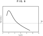
- Fig. 6 shows a result of obtaining, by an experiment, the relationship between the distance D xs (abscissa) and the count (ordinate) of foreign substances FS detected by the X-ray detector 120.
- the count is a total count (peak count), per predetermined time, of energy corresponding to the position of fluorescent X-rays (for example, Ni K ⁇ -rays) exiting from a specific element contained in the foreign substance.
- the distance D xs from the X ray generation portion XG to the inspection plane IP is desirably 5 mm or less, more desirably 4 mm or less, and still more desirably 3 mm or less.
- the X-ray generation tube 101 for example, a sealed transmission microfocus X-ray source of Canon ANELVA, more specifically, the G series, and still more specifically, the G-511 series or G-311 series is useful.
- the inspection method can further include a step of detecting, by the X-ray detection panel 130, X-rays transmitted through the inspection target object IT having the inspection target surface TS, and in the processing step, the output of the X-ray detector 120 and an output of the X-ray detection panel 130 can be processed.
- the processing step can include a step of detecting the existence of the foreign substance FS and the position of the foreign substance FS based on the output of the X-ray detection panel 130.
- the processing step can include a step of detecting the existence of the foreign substance FS, the position of the foreign substance FS, and the size of the foreign substance FS based on the output of the X-ray detection panel 130.
- the inspection plane IP is a target plane on which the inspection target surface TS should be arranged.
- the inspection plane IP is a plane having a predetermined positional relationship with the position of the X-ray detector 120 or the X-ray receiver 121, and alignment of the inspection target surface TS of the inspection target object IT with the inspection plane IP is equivalent to alignment of the inspection target surface TS of the inspection target object IT with the X-ray detector 120 or the X-ray receiver 121.
- the inspection target surface TS of the inspection target object IT in a case where the inspection target surface TS of the inspection target object IT is not positioned on the inspection plane IP, the X-rays XF emitted from the foreign substance FS existing on the inspection target surface TS and totally reflected by the inspection target surface TS do not enter the X-ray receiver 121. In this status, it is impossible to inspect the inspection target surface TS (the foreign substance FS on the inspection target surface TS). Alternatively, in a case where the inspection target surface TS of the inspection target object IT is not positioned on the inspection plane IP, even though it is possible to detect the foreign substance FS, the detection accuracy may be low.
- the controller 140 can be configured to control the adjustment mechanism ADA so as to detect, by the X-ray detector 140, the X-rays XF emitted from the foreign substance FS and totally reflected by the inspection target surface TS.
- the measurement device MD is replaced by a measurement device (for example, an X-ray fluorescence measurement device or an interferometer) configured to measure the characteristic of the inspection target surface TS, and the controller 140 can be configured to control, based on an output of the measurement device, the second adjustment mechanism ADB so as to detect, by the X-ray detector 140, the X-rays XF emitted from the foreign substance FS and totally reflected by the inspection target surface TS.
Landscapes
- Chemical & Material Sciences (AREA)
- Health & Medical Sciences (AREA)
- Physics & Mathematics (AREA)
- Biochemistry (AREA)
- Life Sciences & Earth Sciences (AREA)
- Analytical Chemistry (AREA)
- General Health & Medical Sciences (AREA)
- General Physics & Mathematics (AREA)
- Immunology (AREA)
- Pathology (AREA)
- Crystallography & Structural Chemistry (AREA)
- Toxicology (AREA)
- High Energy & Nuclear Physics (AREA)
- General Engineering & Computer Science (AREA)
- Engineering & Computer Science (AREA)
- Analysing Materials By The Use Of Radiation (AREA)
Abstract
Description
- The present invention relates to an inspection apparatus and an inspection method.
- PTL 1 describes a high-resolution X-ray microscope apparatus with an X-ray fluorescence analysis function, that includes a detector configured to detect fluorescent X-rays which are generated from a sample by focusing electron beams on an X-ray generation target by an object lens and irradiating the sample with X-rays generated from the target, and an analysis unit configured to analyze the fluorescent X-rays from the detection result of the detector. PTL 1 also describes an arrangement in which the whole detector or part of the detector is incorporated in the magnetic circuit of the object lens.
- PTL 1:
Japanese Patent Laid-Open No. 2009-236622 - In recent years, for example, there has been a problem that a foreign substance having a size equal to or smaller than several tens of µm is taken in a product to cause a defect. For example, in a lithium ion battery, with respect to a constituent member using carbon, copper, or aluminum as a material, a micronization of foreign substance of stainless steel or part of the constituent member may be taken in the battery at the time of manufacturing.
- If, at the time of manufacturing a lithium ion battery, a foreign substance is taken in the battery, a separator for maintaining insulation in the battery may break due to a vibration of the foreign substance after shipping of the battery. In this case, the battery may be short-circuited to ignite or explode.
- If a foreign substance can be detected nondestructively, it is possible to prevent distribution of a product that may ignite or explode. As a method of detecting a foreign substance existing on the surface of a sample using X-rays and specifying the element of the foreign substance, there are provided X-ray Fluorescence (to also be called XRF) and Grazing Incidence X-ray Fluorescence (to also be called TXRF). In X-ray Fluorescence, the element of a sample substrate is also excited. In Grazing Incidence X-ray Fluorescence, incident X-rays are scattered due to a foreign substance. Therefore, in these measurement methods, there is a problem that the intensity ratio of the generated fluorescent X-rays becomes low due to the foreign substance.
- The present invention provides a technique advantageous in detecting a foreign substance existing on an inspection target surface with high sensitivity.
- A first aspect of the present invention provides an inspection apparatus for inspecting an inspection target object, comprising: an X-ray generation tube having a target including an X ray generation portion that generates X-rays by irradiation with an electron beam, and configured to emit X-rays to an inspection target surface of the inspection target object; an X-ray detector configured to detect X-rays emitted from a foreign substance existing on the inspection target surface irradiated with the X-rays from the X ray generation portion and totally reflected by the inspection target surface; and an adjustment mechanism configured to adjust a relative position between the inspection target surface and the X-ray detector.
- A second aspect of the present invention provides an inspection method of inspecting an inspection target surface arranged on an inspection plane, comprising: an adjustment step of adjusting a relative position between the inspection plane and the inspection target surface; an X-ray detection step of emitting X-rays to the inspection plane and detecting, by an X-ray detector, X-rays emitted from a foreign substance existing on the inspection target surface and totally reflected by the inspection target surface; and a processing step of processing an output of the X-ray detector.
- According to the present invention, there is provided a technique advantageous in detecting a foreign substance existing on an inspection target surface with high sensitivity.
-
-
Fig. 1 is a view schematically showing the arrangement of an inspection apparatus according to an embodiment; -
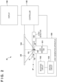
Fig. 2 is a view showing a practical example of the arrangement of the inspection apparatus according to the embodiment; -
Fig. 3 is a view schematically showing an example of the arrangement of an X-ray generation tube; -
Fig. 4 is an enlarged schematic view of part of the inspection apparatus shown inFig. 2 ; -
Fig. 5 is an enlarged schematic view of part of the inspection apparatus shown inFig. 2 ; -
Fig. 6 is a graph exemplifying the relationship between a distance Dxs (abscissa) and the count (ordinate) of foreign substances detected by an X-ray detector; -
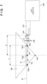
Fig. 7 is a view showing a practical example of the arrangement of the inspection apparatus according to the embodiment; -
Fig. 8 is a view schematically showing the arrangement of the inspection apparatus according to the embodiment; and -
Fig. 9 is a view schematically showing the arrangement of the inspection apparatus according to the embodiment. - Hereinafter, embodiments will be described in detail with reference to the attached drawings. Note, the following embodiments are not intended to limit the scope of the claimed invention. Multiple features are described in the embodiments, but limitation is not made to an invention that requires all such features, and multiple such features may be combined as appropriate. Furthermore, in the attached drawings, the same reference numerals are given to the same or similar configurations, and redundant description thereof is omitted.
-
Fig. 1 schematically shows the arrangement of an inspection apparatus IA according to the embodiment. The inspection apparatus IA can be formed as, for example, an inspection apparatus that inspects an inspection target surface TS arranged on an inspection plane IP. The inspection plane IP is a plane (target plane) on which the inspection target surface TS should be arranged, and the inspection target surface TS is one surface of an inspection target object IT. The inspection apparatus IA can include anX-ray generation tube 101. TheX-ray generation tube 101 has a target (not shown) including an X ray generation portion XG that generates X-rays by irradiation with an electron beam, and emits X-rays XR to the inspection plane IP. A foreign substance FS irradiated with the X-rays XR from the X ray generation portion XG generates X-rays corresponding to a material forming the foreign substance FS, and such X-rays are also called fluorescent X-rays or characteristic X-rays. Some of the X-rays generated by the foreign substance FS irradiated with the X-rays XR are totally reflected by the inspection target surface TS. The X-rays emitted from the foreign substance FS and totally reflected by the inspection target surface TS are represented as X-rays XF. The inspection apparatus IA can include anX-ray detector 120. TheX-ray detector 120 can be configured to detect the X-rays XF emitted from the foreign substance FS existing on the inspection target surface TS irradiated with the X-rays XR from the X ray generation portion XG and totally reflected by the inspection target surface TS. The inspection apparatus IA can further include a processor that performs processing of detecting the foreign substance FS based on an output from theX-ray detector 120. The processor can further perform processing of specifying the material forming the foreign substance FS based on the output from theX-ray detector 120. The processor can be implemented by, for example, a controller that controls the operation of the inspection apparatus IA. -
Fig. 2 shows a practical example of the arrangement of the inspection apparatus IA shown inFig. 1 . The inspection apparatus IA can include anX-ray generation apparatus 100, theX-ray detector 120, and acontroller 140. TheX-ray generation apparatus 100 can include theX-ray generation tube 101 and adriving circuit 103 that drives theX-ray generation tube 101. TheX-ray generation apparatus 100 can further include aboosting circuit 102 that supplies a boosted voltage to thedriving circuit 103. TheX-ray generation apparatus 100 can further include a storage container (not shown) that stores theX-ray generation tube 101, thedriving circuit 103, and theboosting circuit 102, and the storage container can be filled with an insulating fluid such as insulating oil. Thecontroller 140 can be configured to control theX-ray generation apparatus 100 and theX-ray detector 120. Thecontroller 140 can have the function of the above-described processor. More specifically, thecontroller 140 can perform processing of detecting the foreign substance FS based on the output from theX-ray detector 120. Furthermore, thecontroller 140 can perform processing of specifying the material forming the foreign substance FS based on the output from theX-ray detector 120. Thecontroller 140 can be formed by, for example, a PLD (an abbreviation of Programmable Logic Device) such as an FPGA(an abbreviation of Field Programmable Gate Array), an ASIC (an abbreviation of Application Specific Integrated Circuit), a general-purpose or dedicated computer installed with a program, or a combination of all or some of these components. - The inspection apparatus IA may further include an
X-ray detection panel 130 that detects X-rays emitted from the X ray generation portion XG and transmitted through the inspection target object IT having the inspection target surface TS. Thecontroller 140 can be configured to generate an image (a transmission image of the inspection target object IT) of the X-rays transmitted through the inspection target object IT based on an output from theX-ray detection panel 130 and detect the foreign substance FS existing on the inspection target surface TS based on the image. It is possible to detect a foreign substance existing inside the inspection target object IT and a foreign substance existing on a surface on the opposite side of the inspection target surface TS using theX-ray detection panel 130. Thecontroller 140 can be configured to detect the existence of the foreign substance FS and also detect the position and/or size of the foreign substance FS. By providing theX-ray detection panel 130 in addition to theX-ray detector 120, the foreign substance FS that cannot be detected by theX-ray detector 120 can be detected by theX-ray detection panel 130, thereby making it possible to improve the accuracy of detection of the foreign substance FS. As compared with a system including two apparatuses that acquire a transmission image and detect a foreign substance, respectively, the inspection apparatus IA that acquires a transmission image and detects a foreign substance using X-rays emitted from one X-ray generation tube is advantageous in reducing the size and the cost. - The inspection apparatus IA may further include a
display 150, and thecontroller 140 can be configured to display, on thedisplay 150, information indicating the constituent material of the foreign substance FS specified based on the output from theX-ray detector 120. Thecontroller 140 can further be configured to display, on thedisplay 150, the transmission image of the inspection target object IT generated based on the output from theX-ray detection panel 130. In addition, thecontroller 140 can be configured to display, on thedisplay 150, information indicating the position and/or size of the foreign substance detected based on the output from theX-ray detection panel 130. Thecontroller 140 may be formed by a single unit or may be divided into a plurality of units. -
Fig. 3 schematically shows an example of the arrangement of theX-ray generation tube 101. TheX-ray generation tube 101 can include an electron gun EG, ananode 93 having atarget 933 including the X ray generation portion XG that generates X-rays when electrons from the electron gun EG collide, and an insulatingtube 92. In theX-ray generation tube 101, theanode 93 can be arranged to close one of the two opening ends of the insulatingtube 92, and a closingmember 91 including the electron gun EG can be arranged to close the other of the two opening ends of the insulatingtube 92. Adeflector 94 that deflects the flow (electron beam) of electrons from the electron gun EG may be arranged outside the insulatingtube 92. TheX-ray generation tube 101 shown inFig. 3 is an example of a sealed transmission type X-ray generation tube in which the internal space of the insulatingtube 92 is maintained in a vacuum state and X-rays are transmitted through thetarget 933 and a target holding plate 932 (to be described later). However, as theX-ray generation tube 101, an unsealed open type or non-transmission reflection type X-ray generation tube may be adopted. - The
deflector 94 can be arranged outside theX-ray generation tube 101. With respect to a direction parallel to an axis AX of theX-ray generation tube 101, thedeflector 94 can be provided between theanode 93 and a cathode (not shown). In an example, with respect to the direction parallel to the axis AX of theX-ray generation tube 101, thedeflector 94 is provided between the electron gun EG and thetarget 933. More specifically, avirtual plane 97 crossing thedeflector 94 can be located in a space sandwiched between a virtual plane 95 contacting the distal end of the electron gun EG and avirtual plane 96 contacting part of thetarget 933. Thevirtual planes X-ray generation tube 101. - The
anode 93 can include thetarget 933, thetarget holding plate 932 that holds thetarget 933, and anelectrode 931 that holds thetarget holding plate 932. Theelectrode 931 is electrically connected to thetarget 933 and can give a potential to thetarget 933. Thetarget 933 generates X-rays when electrons (electron beam) emitted from the electron gun EG collide against thetarget 933. The X ray generation portion XG is a portion of the surface of thetarget 933, against which the electrons (electron beam) collide. The X-rays generated by the X ray generation portion XG are transmitted through thetarget holding plate 932 and emitted to the outside of theX-ray generation tube 101. Theanode 93 can be maintained at, for example, the ground potential but may be maintained at another potential. - The
target 933 is made of a metal material. Thetarget 933 is desirably made of a material having a high melting point, for example, tungsten, tantalum, molybdenum, or the like, which contributes to improvement of X-ray generation efficiency. Thetarget holding plate 932 can be made of a material that readily passes X-rays, for example, beryllium, diamond, or the like. Thetarget holding plate 932 is desirably made of diamond. This can decrease the thickness of thetarget holding plate 932 while maintaining the strength of thetarget holding plate 932, and can decrease the distance between the inspection plane IP (inspection target surface TS) and the target 933 (X ray generation portion XG). The thickness of thetarget holding plate 932 is desirably thin. More specifically, the thickness of thetarget holding plate 932 is desirably 4 mm or less, and more desirably 2 mm or less, 1 mm or less, or 0.3 mm or less. The thickness of thetarget holding plate 932 can be set with reference to the distance from the X ray generation portion XG to the inspection plane IP, which is necessary to specify an element contained in the foreign substance (to be described later). To specify the element contained in the foreign substance, thetarget holding plate 932 is desirably, extremely thin. However, thetarget holding plate 932 is desirably thick in terms of the processing cost and the individual difference of thetarget holding plate 932, strength for maintaining the internal space of the insulatingtube 92 in the vacuum state, and the like. Therefore, the optimum thickness of thetarget holding plate 932 is desirably used. Note thatFig. 3 is not intended to show the relationship between the thickness of thetarget 933 and that of thetarget holding plate 932. For example, the thickness of thetarget 933 may be several µm, and the thickness of thetarget holding plate 932 may be several hundred µm. -
Fig. 4 is an enlarged schematic view of part of the inspection apparatus IA shown inFig. 2 . The foreign substance FS can exist on the inspection target surface TS. The X-rays (characteristic X-rays) XF that are emitted from the foreign substance FS so as to be totally reflected by the inspection target surface TS and are totally reflected by the inspection target surface TS enter anX-ray receiver 121 of theX-ray detector 120. On the other hand, fluorescent X-rays that can be generated from the inspection target object IT by irradiation with the X-rays XR from the X ray generation portion XG hardly enter theX-ray receiver 121 of theX-ray detector 120 arranged to detect the X-rays (characteristic X-rays) XF. Therefore, the ratio of the fluorescent X-rays emitted from the inspection target object IT and detected by theX-ray detector 120 with respect to the X-rays (characteristic X-rays) XF emitted from the foreign substance FS and detected by theX-ray detector 120 can be made extremely low. - The
X-ray detector 120 may be a silicon drift detector (SDD), a CdTe detector, or a CdZnTe detector. TheX-ray detector 120 may be an energy dispersion detector. If theX-ray detector 120 is an energy dispersion detector, the controller (or processor) 140 can decide the material or element forming the foreign substance FS based on the elemental profile of energy dispersion (a count value for each energy). Commercial software may be installed on the controller (or processor) 140 to decide the material or element forming the foreign substance FS. Examples of such software are, for example, "XRS-FP Quantitative XRF Analysis Software" of AMETEK or UniQuant software. - The specifications of the
X-ray detector 120 can be decided in accordance with an energy resolution necessary to detect a foreign substance. An example of a detector having a low energy resolution can be a detector using a scintillator, an Si PIN photodiode, or a CCD. An example of a detector having an even higher energy resolution can be a detector using a proportional counter. An example of a detector having an even higher energy resolution can be a detector applied with a CdTe direct-bandgap crystal or an energy dispersion detection method like an Si drift detector. An example of a detector having an even higher energy resolution can be a detector applied with a wavelength dispersion detection method of obtaining energy from an angle using an analyzing crystal. - To totally reflect, by the inspection target surface TS, the fluorescent X-rays from the foreign substance FS, an angle at which the fluorescent X-rays from the foreign substance FS enter the inspection target surface TS needs to be a total reflection critical angle θc or less.

- θc: total reflection critical angle
- re: classical electron radius (2.818 × 10⁻¹⁵ m)
- N0: Avogadro number
- λ: X-ray wavelength
- ρ: density (g/cm3)
- Zi, Mi, xi: atomic number, atomic weight, and atomic ratio (molar ratio) of ith atom
- fi: atomic scattering factor (anomalous dispersion term) of ith atom
- If the inspection target surface TS is made of a metal, the total reflection critical angle is theoretically about 1° or less. However, in fact, the metal surface is often oxidized or carbonized, or a reflection critical angle different from the theoretical value is often obtained because, for example, the surface is covered with a graphite layer. If a total reflection condition is satisfied when the inspection target surface TS is irradiated with the X-rays XR, an angle (total reflection critical angle) formed by the inspection target surface TS and the characteristic X-rays XF emitted from the foreign substance FS and totally reflected by the inspection target surface TS is confirmed to be 5° or less through an experiment. At this time, since the foreign substance FS is extremely small as compared with a distance Dxs between the X ray generation portion XG and the inspection plane IP (inspection target surface TS), a position at which the X-rays emitted from the foreign substance FS are totally reflected by the inspection target surface TS may be regarded as a position at which the X-rays XR from the X ray generation portion XG enter the inspection plane IP. If the foreign substance FS exists at a position where the X-rays XR from the X ray generation portion XG vertically enter the inspection plane IP, as shown in
Fig. 4 , the position at which the X-rays emitted from the foreign substance FS are totally reflected by the inspection target surface TS may be regarded as the position at which the X-rays XR from the X ray generation portion XG vertically enter the inspection plane IP. - Since the total reflection critical angle is 5° or less, an angle θ formed by the inspection plane IP and a virtual line connecting the
X-ray receiver 121 of theX-ray detector 120 and the position at which the X-rays XR from the X ray generation portion XG enter the inspection plane IP (an angle formed by the inspection plane IP and a virtual line connecting the center of the X-ray receiver of theX-ray detector 120 and the intersection point of the inspection plane IP and the axis of the X-ray generation tube 101) can be set to 5° or less, desirably 2° or less, and more desirably 1° or less. As the angle θ is smaller, the ratio of the fluorescent X-rays emitted from the inspection target object IT and detected by theX-ray detector 120 with respect to the X-rays (characteristic X-rays) XF emitted from the foreign substance FS and detected by theX-ray detector 120 can be made lower. - The
X-ray detector 120 can be arranged at a position where the extension plane of the inspection plane IP crosses theX-ray detector 120. As schematically shown inFig. 5 , theX-ray receiver 121 can include awindow portion 122 that passes the X-rays XF. Thewindow portion 122 can have, for example, a diameter of several mm and a thickness of several hundred µm. Thewindow portion 122 can be made of, for example, beryllium. As schematically shown inFig. 5 , the inspection apparatus IA may include aslit member 125 having a slit (opening) on a virtual line connecting theX-ray receiver 121 of theX-ray detector 120 and the position at which the X-rays XR from the X ray generation portion XG enter the inspection plane IP. The size of the slit provided in theslit member 125 and the arrangement position of theX-ray detector 120 can be decided in accordance with a range irradiated with the X-rays XR on the inspection target surface TS, the materials that can form the inspection target surface TS and the foreign substance FS, and the like. Consider a case in which foreign substances FS 1 and FS3 exist at two ends of a width Y irradiated with the X-rays XR on the inspection target surface TS, and a distance Z from the center of the width Y to theX-ray receiver 121 has the same length as that of the width Y, as schematically shown inFig. 7 . In this case, by setting the lower limit of a width Ws of the slit to Y × tanθ, and setting a distance X2 between the center of theX-ray receiver 121 and the inspection plane IP to Y × tanθ, it is possible to detect all foreign substances within the range irradiated with the X-rays XR on the inspection target surface TS. - To increase the intensity of the X-rays XF detected by the
X-ray detector 120, the distance Dxs from the X ray generation portion XG to the inspection plane IP is desirably made small.Fig. 6 shows a result of obtaining, by an experiment, the relationship between the distance Dxs (abscissa) and the count (ordinate) of foreign substances FS detected by theX-ray detector 120. The count is a total count (peak count), per predetermined time, of energy corresponding to the position of fluorescent X-rays (for example, Ni Kα-rays) exiting from a specific element contained in the foreign substance. Considering a count TH necessary to specify the element, the distance Dxs from the X ray generation portion XG to the inspection plane IP is desirably 5 mm or less, more desirably 4 mm or less, and still more desirably 3 mm or less. As theX-ray generation tube 101, for example, a sealed transmission microfocus X-ray source of Canon ANELVA, more specifically, the G series, and still more specifically, the G-511 series or G-311 series is useful. - To detect, by a transmission image, a foreign substance having a size of several µm to several tens of µm with high sensitivity, a distance Dsf from the inspection plane IP to the
X-ray detection panel 130 needs to be made sufficiently larger than Dxs. For example, if 10 pixels are necessary to detect a foreign substance having a diameter of 5 µm, when an X-ray detection panel (FPD) having a pixel pitch of 100 µm is used, a magnification ratio of 100 × 10/5 = 200 is required for detection. As for a foreign substance having a diameter of 50 µm, a magnification ratio of 20 is required for detection. Therefore, Dsf/Dxs is set to desirably 20 or more, and more desirably 200 or more. This can detect a foreign substance with high sensitivity using a transmission image. - The inspection apparatus IA is useful to detect a foreign substance attached to a material of a lithium ion battery in a manufacturing step of the lithium ion battery, but is merely an example and is also useful for other application purposes. For example, the inspection apparatus IA may be used to measure and analyze airborne particles such as PM2.5 influencing the environment and health. In this case, by using the inspection apparatus IA for the conventional technique of periodically (for example, every hour or every day) measuring the number of particles and the sizes of the particles, it is possible to simultaneously specify materials or elements forming the particles in addition to measurement of the number of particles and the sizes of the particles, thereby implementing more advanced environmental and health measures. Alternatively, by using the inspection apparatus IA for the field of semiconductors, micronization of which has recently been advanced, such as an "EUV mask manufacturing apparatus, an inspection apparatus, and an inspection apparatus of a semiconductor manufacturing step, it is possible to improve a yield and early solve the cause of an abnormality using the element information of a foreign substance.
- An inspection method of inspecting the inspection target surface TS arranged on the inspection plane IP using the inspection apparatus IA will be described below. The inspection method can include an X-ray detection step of emitting X-rays to the inspection plane IP (inspection target surface TS) and detecting, by the
X-ray detector 120, the X-rays XF emitted from the foreign substance FS existing on the inspection target surface TS and totally reflected by the inspection target surface TS, and a processing step of processing an output of theX-ray detector 120. The processing step can include a step of detecting the foreign substance FS and/or a step of specifying a material forming the foreign substance FS. The inspection method can further include a step of detecting, by theX-ray detection panel 130, X-rays transmitted through the inspection target object IT having the inspection target surface TS, and in the processing step, the output of theX-ray detector 120 and an output of theX-ray detection panel 130 can be processed. The processing step can include a step of detecting the existence of the foreign substance FS and the position of the foreign substance FS based on the output of theX-ray detection panel 130. Alternatively, the processing step can include a step of detecting the existence of the foreign substance FS, the position of the foreign substance FS, and the size of the foreign substance FS based on the output of theX-ray detection panel 130. - The above description assumes that the inspection target surface TS is aligned with the inspection plane IP. In this example, the inspection plane IP is a target plane on which the inspection target surface TS should be arranged. In other words, the inspection plane IP is a plane having a predetermined positional relationship with the position of the
X-ray detector 120 or theX-ray receiver 121, and alignment of the inspection target surface TS of the inspection target object IT with the inspection plane IP is equivalent to alignment of the inspection target surface TS of the inspection target object IT with theX-ray detector 120 or theX-ray receiver 121. As shown inFig. 8 , in a case where the inspection target surface TS of the inspection target object IT is not positioned on the inspection plane IP, the X-rays XF emitted from the foreign substance FS existing on the inspection target surface TS and totally reflected by the inspection target surface TS do not enter theX-ray receiver 121. In this status, it is impossible to inspect the inspection target surface TS (the foreign substance FS on the inspection target surface TS). Alternatively, in a case where the inspection target surface TS of the inspection target object IT is not positioned on the inspection plane IP, even though it is possible to detect the foreign substance FS, the detection accuracy may be low. - To cope with this, as schematically shown in
Figs. 8 and9 , the inspection apparatus IA preferably includes an adjustment mechanism ADA configured to adjust the relative position between the inspection target surface TS of the inspection target object IT and the X-ray detector 120 (in other words, the inspection plane IP). As schematically shown inFig. 9 , thecontroller 140 can control the adjustment mechanism ADA so that the inspection target surface TS of the inspection target object IT coincides with the inspection plane IP. The inspection apparatus IA may include a measurement device MD configured to measure the position of the inspection target surface TS of the inspection target object IT. The measurement device MD may be, for example, a noncontact type device (for example, an interferometer) or a contact type device. - The
controller 140 can be configured to control, based on an output of the measurement device MD, the adjustment mechanism ADA so as to detect, by theX-ray detector 140, the X-rays XF emitted from the foreign substance FS and totally reflected by the inspection target surface TS. The inspection apparatus IA may further include a second adjustment mechanism ADB configured to adjust the position of theslit member 125. Thecontroller 140 can be configured to control, based on the output of the measurement device MD, the second adjustment mechanism ADB so as to detect, by theX-ray detector 140, the X-rays XF emitted from the foreign substance FS and totally reflected by the inspection target surface TS. - The inspection target surface TS of the inspection target object IT may not coincide with the inspection plane IP in, for example, a case where the inspection target object IT has an error with respect to a target dimension, a case where a vibration occurs, or the like. Furthermore, even if the inspection target surface TS of the inspection target object IT coincides with the inspection plane IP, in a case where the inspection target surface TS of the inspection target object IT has no target characteristic, the total reflection critical angle is shifted from a design value, thereby causing a phenomenon that the X-rays XF totally reflected by the inspection target surface TS do not enter the
X-ray receiver 121 of theX-ray detector 140. In this case as well, thecontroller 140 can be configured to control the adjustment mechanism ADA so as to detect, by theX-ray detector 140, the X-rays XF emitted from the foreign substance FS and totally reflected by the inspection target surface TS. In this case, the measurement device MD is replaced by a measurement device (for example, an X-ray fluorescence measurement device or an interferometer) configured to measure the characteristic of the inspection target surface TS, and thecontroller 140 can be configured to control, based on an output of the measurement device, the second adjustment mechanism ADB so as to detect, by theX-ray detector 140, the X-rays XF emitted from the foreign substance FS and totally reflected by the inspection target surface TS. - The relative position between the inspection target surface TS and the X-ray detector 120 (in other words, the inspection plane IP) may be adjusted using an inspection target object for adjustment when the
controller 140 controls the adjustment mechanism ADA so as to detect, by theX-ray detector 140, the X-rays XF emitted from a foreign substance on the inspection target object for adjustment and totally reflected by the inspection target surface TS. The same applies to adjustment of theslit member 125 by the 12th adjustment mechanism ADB. - The present invention is not limited to the above embodiments and various changes and modifications can be made within the spirit and scope of the present invention. Therefore, to apprise the public of the scope of the present invention, the following claims are made.
Claims (21)
- An inspection apparatus for inspecting an inspection target object, comprising:an X-ray generation tube having a target including an X ray generation portion that generates X-rays by irradiation with an electron beam, and configured to emit X-rays to an inspection target surface of the inspection target object;an X-ray detector configured to detect X-rays emitted from a foreign substance existing on the inspection target surface irradiated with the X-rays from the X ray generation portion and totally reflected by the inspection target surface; andan adjustment mechanism configured to adjust a relative position between the inspection target surface and the X-ray detector.
- The inspection apparatus according to claim 1, further comprising:a measurement device configured to measure a position of the inspection target surface; anda controller configured to control, based on an output of the measurement device, the adjustment mechanism so as to detect, by the X-ray detector, the X-rays totally reflected by the inspection target surface.
- The inspection apparatus according to claim 1 or 2, wherein the controller performs processing of detecting the foreign substance based on an output from the X-ray detector.
- The inspection apparatus according to claim 3, wherein the controller further performs processing of specifying a material forming the foreign substance.
- The inspection apparatus according to any one of claims 1 to 4, wherein a distance between the X ray generation portion and an inspection plane as a target plane on which the inspection target surface should be arranged is not larger than 5 mm.
- The inspection apparatus according to any one of claims 1 to 4, wherein a distance between the X ray generation portion and an inspection plane as a target plane on which the inspection target surface should be arranged is not larger than 3 mm.
- The inspection apparatus according to any one of claims 1 to 6, wherein an angle formed by the inspection plane and a virtual line connecting a center of an X-ray receiver of the X-ray detector and an intersection point of an axis of the X ray generation portion and the inspection plane as the target plane on which the inspection target surface should be arranged is not larger than 5°.
- The inspection apparatus according to any one of claims 1 to 6, wherein an angle formed by the inspection plane and a virtual line connecting a center of an X-ray receiver of the X-ray detector and an intersection point of an axis of the X ray generation portion and the inspection plane as the target plane on which the inspection target surface should be arranged is not larger than 2°.
- The inspection apparatus according to claim 7 or 8, further comprising a slit member having a slit on the virtual line.
- The inspection apparatus according to claim 9, further comprising a second adjustment mechanism configured to adjust a position of the slit member.
- The inspection apparatus according to any one of claims 1 to 10, further comprising an X-ray detection panel configured to detect X-rays emitted from the X-ray generation portion and transmitted through an inspection target object having the inspection target surface.
- The inspection apparatus according to any one of claims 1 to 11, wherein the X-ray generation tube is of a sealed transmission type.
- The inspection apparatus according to any one of claims 1 to 12, wherein the X-ray generation tube includes a target holding plate configured to hold the target, and a thickness of the target holding plate is not larger than 4 mm.
- The inspection apparatus according to claim 13, wherein the target holding plate contains diamond.
- An inspection method of inspecting an inspection target surface arranged on an inspection plane, comprising:an adjustment step of adjusting a relative position between the inspection plane and the inspection target surface;an X-ray detection step of emitting X-rays to the inspection plane and detecting, by an X-ray detector, X-rays emitted from a foreign substance existing on the inspection target surface and totally reflected by the inspection target surface; anda processing step of processing an output of the X-ray detector.
- The inspection method according to claim 15, wherein the processing step includes a step of detecting the foreign substance.
- The inspection method according to claim 15 or 16, wherein the processing step includes a step of specifying a material forming the foreign substance.
- The inspection method according to any one of claims 15 to 17, further comprising a step of detecting, by an X-ray detection panel, X-rays transmitted through an inspection target object having the inspection target surface,
wherein in the processing step, the output of the X-ray detector and an output of the X-ray detection panel are processed. - The inspection method according to claim 18, wherein the processing step includes a step of detecting existence of the foreign substance and a position of the foreign substance based on the output of the X-ray detection panel.
- The inspection method according to claim 18, wherein the processing step includes a step of detecting existence of the foreign substance, a position of the foreign substance, and a size of the foreign substance based on the output of the X-ray detection panel.
- The inspection method according to any one of claims 14 to 20, wherein the adjustment step includesa step of measuring a position of the inspection target surface, anda step of adjustment a position of the X-ray detector in accordance with the measurement of the position of the inspection target surface.
Applications Claiming Priority (2)
| Application Number | Priority Date | Filing Date | Title |
|---|---|---|---|
| JP2022013653 | 2022-01-31 | ||
| PCT/JP2022/043907 WO2023145237A1 (en) | 2022-01-31 | 2022-11-29 | Inspection device and inspection method |
Publications (2)
| Publication Number | Publication Date |
|---|---|
| EP4474803A1 true EP4474803A1 (en) | 2024-12-11 |
| EP4474803A4 EP4474803A4 (en) | 2026-01-14 |
Family
ID=87471017
Family Applications (5)
| Application Number | Title | Priority Date | Filing Date |
|---|---|---|---|
| EP22923964.5A Pending EP4474800A4 (en) | 2022-01-31 | 2022-03-31 | INSPECTION DEVICE AND INSPECTION PROCEDURES |
| EP22924089.0A Pending EP4474803A4 (en) | 2022-01-31 | 2022-11-29 | INSPECTION DEVICE AND INSPECTION PROCEDURES |
| EP22924088.2A Pending EP4474802A4 (en) | 2022-01-31 | 2022-11-29 | IDENTIFICATION DEVICE FOR DETECTING FOREIGN BODYs AND OPERATION WITH FLUORESCENT X-RAY |
| EP22924087.4A Pending EP4474801A4 (en) | 2022-01-31 | 2022-11-29 | INSPECTION DEVICE AND INSPECTION PROCEDURES |
| EP22924090.8A Pending EP4474804A4 (en) | 2022-01-31 | 2022-11-29 | INSPECTION DEVICE AND INSPECTION PROCEDURES |
Family Applications Before (1)
| Application Number | Title | Priority Date | Filing Date |
|---|---|---|---|
| EP22923964.5A Pending EP4474800A4 (en) | 2022-01-31 | 2022-03-31 | INSPECTION DEVICE AND INSPECTION PROCEDURES |
Family Applications After (3)
| Application Number | Title | Priority Date | Filing Date |
|---|---|---|---|
| EP22924088.2A Pending EP4474802A4 (en) | 2022-01-31 | 2022-11-29 | IDENTIFICATION DEVICE FOR DETECTING FOREIGN BODYs AND OPERATION WITH FLUORESCENT X-RAY |
| EP22924087.4A Pending EP4474801A4 (en) | 2022-01-31 | 2022-11-29 | INSPECTION DEVICE AND INSPECTION PROCEDURES |
| EP22924090.8A Pending EP4474804A4 (en) | 2022-01-31 | 2022-11-29 | INSPECTION DEVICE AND INSPECTION PROCEDURES |
Country Status (7)
| Country | Link |
|---|---|
| US (6) | US11921059B2 (en) |
| EP (5) | EP4474800A4 (en) |
| JP (6) | JP7667882B2 (en) |
| KR (5) | KR20240141192A (en) |
| CN (5) | CN118661094A (en) |
| TW (6) | TW202433050A (en) |
| WO (5) | WO2023145101A1 (en) |
Families Citing this family (1)
| Publication number | Priority date | Publication date | Assignee | Title |
|---|---|---|---|---|
| WO2023145101A1 (en) * | 2022-01-31 | 2023-08-03 | キヤノンアネルバ株式会社 | Inspection device and inspection method |
Family Cites Families (55)
| Publication number | Priority date | Publication date | Assignee | Title |
|---|---|---|---|---|
| JPH01244344A (en) * | 1988-03-25 | 1989-09-28 | Hitachi Ltd | Apparatus for measuring x-ray absorbing spectrum |
| JPH07119717B2 (en) * | 1989-12-12 | 1995-12-20 | シャープ株式会社 | Semiconductor material evaluation equipment |
| JPH0534131A (en) * | 1991-08-05 | 1993-02-09 | Fujitsu Ltd | Image processing method and image processing apparatus |
| JPH05346411A (en) * | 1992-04-16 | 1993-12-27 | Rigaku Denki Kogyo Kk | Fluorescent x-ray analyzer |
| EP0697109B1 (en) * | 1994-03-02 | 1999-07-14 | Koninklijke Philips Electronics N.V. | X-ray spectrometer with a grazing take-off angle |
| JP3165615B2 (en) * | 1995-03-17 | 2001-05-14 | 財団法人国際超電導産業技術研究センター | Surface elemental analysis method and device |
| KR100233312B1 (en) | 1995-08-09 | 1999-12-01 | 야마모토 카즈모토 | Total reflection fluorescence X-ray analysis apparatus and method |
| US5742658A (en) * | 1996-05-23 | 1998-04-21 | Advanced Micro Devices, Inc. | Apparatus and method for determining the elemental compositions and relative locations of particles on the surface of a semiconductor wafer |
| JPH09318565A (en) * | 1996-05-24 | 1997-12-12 | Rigaku Ind Co | X-ray analyzing method and apparatus therefor |
| JP2984232B2 (en) * | 1996-10-25 | 1999-11-29 | 株式会社テクノス研究所 | X-ray analyzer and X-ray irradiation angle setting method |
| US6005915A (en) | 1997-11-07 | 1999-12-21 | Advanced Micro Devices, Inc. | Apparatus and method for measuring the roughness of a target material surface based upon the scattering of incident X-ray photons |
| US6108398A (en) | 1998-07-13 | 2000-08-22 | Jordan Valley Applied Radiation Ltd. | X-ray microfluorescence analyzer |
| JP2000055841A (en) * | 1998-08-13 | 2000-02-25 | Fujitsu Ltd | X-ray analysis method |
| DE19934987B4 (en) | 1999-07-26 | 2004-11-11 | Fraunhofer-Gesellschaft zur Förderung der angewandten Forschung e.V. | X-ray anode and its use |
| DE19948382A1 (en) * | 1999-10-07 | 2001-05-03 | Gemetec Ges Fuer Mestechnik Un | Large wafer area detector |
| JP2001208708A (en) | 2000-01-31 | 2001-08-03 | Japan Science & Technology Corp | Method and apparatus for analyzing foreign matter by oblique emission electron probe micro X-ray analysis |
| US6829327B1 (en) * | 2000-09-22 | 2004-12-07 | X-Ray Optical Systems, Inc. | Total-reflection x-ray fluorescence apparatus and method using a doubly-curved optic |
| JP2002202272A (en) | 2000-12-28 | 2002-07-19 | Shimadzu Corp | X-ray fluoroscope |
| JP3673825B2 (en) | 2001-03-27 | 2005-07-20 | 独立行政法人物質・材料研究機構 | Oblique X-ray analysis method |
| JP3998556B2 (en) * | 2002-10-17 | 2007-10-31 | 株式会社東研 | High resolution X-ray microscope |
| US7065176B2 (en) | 2003-05-28 | 2006-06-20 | General Electric Company | Method and system to inspect a component |
| JP2005121468A (en) * | 2003-10-16 | 2005-05-12 | Tohken Co Ltd | Food foreign matter inspection equipment such as hair using fluorescent X-rays |
| JP2005292077A (en) * | 2004-04-05 | 2005-10-20 | Fuji Electric Holdings Co Ltd | X-ray microscope equipment |
| US7916834B2 (en) | 2007-02-12 | 2011-03-29 | Thermo Niton Analyzers Llc | Small spot X-ray fluorescence (XRF) analyzer |
| JP2007212468A (en) * | 2007-03-16 | 2007-08-23 | Tohken Co Ltd | High resolution X-ray microscopic inspection system |
| JP5127313B2 (en) | 2007-06-15 | 2013-01-23 | 義久 石黒 | Inspection system |
| JP2009075018A (en) * | 2007-09-21 | 2009-04-09 | Technos:Kk | Fluorescent x-ray analysis apparatus, and fluorescent x-ray analysis method |
| JP5489412B2 (en) | 2008-03-26 | 2014-05-14 | 株式会社マーストーケンソリューション | High resolution X-ray microscope with X-ray fluorescence analysis function |
| JP5292323B2 (en) | 2010-01-25 | 2013-09-18 | 株式会社リガク | Micro X-ray measuring device |
| JP4914514B2 (en) | 2010-07-02 | 2012-04-11 | 株式会社リガク | X-ray fluorescence analyzer and method |
| JP5887760B2 (en) * | 2011-08-24 | 2016-03-16 | 富士通株式会社 | Semiconductor device inspection method and semiconductor device manufacturing method |
| JP5881159B2 (en) | 2012-03-27 | 2016-03-09 | 株式会社リガク | Inspection device for different substances and inspection method for different substances |
| US9194828B2 (en) * | 2012-05-22 | 2015-11-24 | Aribex, Inc. | Handheld x-ray system for 3D scatter imaging |
| US20140067316A1 (en) * | 2012-08-30 | 2014-03-06 | Kabushiki Kaisha Toshiba | Measuring apparatus, detector deviation monitoring method and measuring method |
| JP6026936B2 (en) | 2013-03-28 | 2016-11-16 | 株式会社日立ハイテクサイエンス | Foreign object detection device |
| US9551677B2 (en) * | 2014-01-21 | 2017-01-24 | Bruker Jv Israel Ltd. | Angle calibration for grazing-incidence X-ray fluorescence (GIXRF) |
| US9594036B2 (en) * | 2014-02-28 | 2017-03-14 | Sigray, Inc. | X-ray surface analysis and measurement apparatus |
| EP2927948A1 (en) | 2014-04-04 | 2015-10-07 | Nordson Corporation | X-ray inspection apparatus for inspecting semiconductor wafers |
| CN107076684B (en) | 2014-09-02 | 2021-04-02 | 株式会社尼康 | Measurement processing device, measurement processing method, and measurement processing program |
| WO2016059673A1 (en) * | 2014-10-14 | 2016-04-21 | 株式会社リガク | X-ray thin film inspection device |
| DE112015006104B4 (en) * | 2015-03-25 | 2022-05-19 | Hitachi High-Tech Corporation | ELECTRON MICROSCOPE |
| WO2017003665A1 (en) * | 2015-06-30 | 2017-01-05 | Illinois Tool Works Inc. | Inline x-ray measurement apparatus and method |
| US10295486B2 (en) * | 2015-08-18 | 2019-05-21 | Sigray, Inc. | Detector for X-rays with high spatial and high spectral resolution |
| WO2017104659A1 (en) * | 2015-12-15 | 2017-06-22 | 株式会社堀場製作所 | X-ray tube and x-ray spectrometer |
| CN105758345B (en) * | 2016-04-22 | 2018-06-05 | 武汉科技大学 | A kind of x-ray fluorescence imaging device of on-line measurement strip coating thickness |
| CN206020314U (en) * | 2016-09-09 | 2017-03-15 | 广州市怡文环境科技股份有限公司 | A kind of total reflection X-ray fluorescence analysis system |
| JP6867224B2 (en) * | 2017-04-28 | 2021-04-28 | 浜松ホトニクス株式会社 | X-ray tube and X-ray generator |
| US10895541B2 (en) | 2018-01-06 | 2021-01-19 | Kla-Tencor Corporation | Systems and methods for combined x-ray reflectometry and photoelectron spectroscopy |
| JP2019215205A (en) | 2018-06-12 | 2019-12-19 | ローム株式会社 | Imaging device, imaging method and inspection device |
| JP6601854B1 (en) * | 2018-06-21 | 2019-11-06 | 株式会社リガク | X-ray fluorescence analysis system |
| JP7153525B2 (en) * | 2018-10-12 | 2022-10-14 | アンリツ株式会社 | X-ray inspection device |
| JP7270637B2 (en) | 2018-10-25 | 2023-05-10 | 株式会社堀場製作所 | X-ray analyzer and X-ray generation unit |
| CN113877059B (en) | 2020-07-03 | 2025-12-09 | 何浩明 | Clothing structure with adjusting mechanism for attaching patch unit to human body |
| CN114486971A (en) | 2022-01-25 | 2022-05-13 | 深圳市埃芯半导体科技有限公司 | Multi-source designed X-ray analysis system and method |
| WO2023145101A1 (en) * | 2022-01-31 | 2023-08-03 | キヤノンアネルバ株式会社 | Inspection device and inspection method |
-
2022
- 2022-03-31 WO PCT/JP2022/016709 patent/WO2023145101A1/en not_active Ceased
- 2022-03-31 EP EP22923964.5A patent/EP4474800A4/en active Pending
- 2022-03-31 CN CN202280090523.2A patent/CN118661094A/en active Pending
- 2022-03-31 KR KR1020247028367A patent/KR20240141192A/en active Pending
- 2022-11-29 CN CN202280090513.9A patent/CN118891514A/en not_active Withdrawn
- 2022-11-29 JP JP2023576658A patent/JP7667882B2/en active Active
- 2022-11-29 JP JP2023576656A patent/JP7667321B2/en active Active
- 2022-11-29 EP EP22924089.0A patent/EP4474803A4/en active Pending
- 2022-11-29 WO PCT/JP2022/043908 patent/WO2023145238A1/en not_active Ceased
- 2022-11-29 EP EP22924088.2A patent/EP4474802A4/en active Pending
- 2022-11-29 CN CN202280090524.7A patent/CN118679379A/en not_active Withdrawn
- 2022-11-29 KR KR1020247028350A patent/KR20240141191A/en not_active Withdrawn
- 2022-11-29 WO PCT/JP2022/043906 patent/WO2023145236A1/en not_active Ceased
- 2022-11-29 JP JP2023576659A patent/JP7667883B2/en active Active
- 2022-11-29 KR KR1020247027476A patent/KR20240136405A/en not_active Withdrawn
- 2022-11-29 EP EP22924087.4A patent/EP4474801A4/en active Pending
- 2022-11-29 JP JP2023576657A patent/JP7667322B2/en active Active
- 2022-11-29 KR KR1020247027603A patent/KR20240136411A/en not_active Withdrawn
- 2022-11-29 WO PCT/JP2022/043905 patent/WO2023145235A1/en not_active Ceased
- 2022-11-29 CN CN202280090521.3A patent/CN118661093A/en not_active Withdrawn
- 2022-11-29 KR KR1020247028368A patent/KR20240135667A/en active Pending
- 2022-11-29 EP EP22924090.8A patent/EP4474804A4/en active Pending
- 2022-11-29 CN CN202280090522.8A patent/CN118901003A/en active Pending
- 2022-11-29 WO PCT/JP2022/043907 patent/WO2023145237A1/en not_active Ceased
-
2023
- 2023-01-06 JP JP2023001301A patent/JP7615183B2/en active Active
- 2023-01-19 TW TW113116471A patent/TW202433050A/en unknown
- 2023-01-19 TW TW112102600A patent/TWI846289B/en active
- 2023-01-30 TW TW112103027A patent/TWI866041B/en active
- 2023-01-30 TW TW112103028A patent/TWI845135B/en active
- 2023-01-30 TW TW112103029A patent/TWI874900B/en active
- 2023-01-30 TW TW112103030A patent/TWI845136B/en active
- 2023-07-11 US US18/350,093 patent/US11921059B2/en active Active
- 2023-07-11 US US18/350,361 patent/US12241848B2/en active Active
- 2023-07-11 US US18/350,054 patent/US11927554B2/en active Active
- 2023-07-11 US US18/350,255 patent/US11971370B2/en active Active
- 2023-07-11 US US18/350,221 patent/US11977038B2/en active Active
-
2024
- 2024-07-18 US US18/776,818 patent/US20240369502A1/en active Pending
- 2024-12-26 JP JP2024230910A patent/JP2025039599A/en active Pending
Also Published As
Similar Documents
| Publication | Publication Date | Title |
|---|---|---|
| JP2002107134A (en) | Thickness meter for x-ray fluorescence film | |
| US20240369502A1 (en) | Inspection apparatus and inspection method |
Legal Events
| Date | Code | Title | Description |
|---|---|---|---|
| STAA | Information on the status of an ep patent application or granted ep patent |
Free format text: STATUS: THE INTERNATIONAL PUBLICATION HAS BEEN MADE |
|
| PUAI | Public reference made under article 153(3) epc to a published international application that has entered the european phase |
Free format text: ORIGINAL CODE: 0009012 |
|
| STAA | Information on the status of an ep patent application or granted ep patent |
Free format text: STATUS: REQUEST FOR EXAMINATION WAS MADE |
|
| 17P | Request for examination filed |
Effective date: 20240326 |
|
| AK | Designated contracting states |
Kind code of ref document: A1 Designated state(s): AL AT BE BG CH CY CZ DE DK EE ES FI FR GB GR HR HU IE IS IT LI LT LU LV MC ME MK MT NL NO PL PT RO RS SE SI SK SM TR |
|
| DAV | Request for validation of the european patent (deleted) | ||
| DAX | Request for extension of the european patent (deleted) | ||
| A4 | Supplementary search report drawn up and despatched |
Effective date: 20251217 |
|
| RIC1 | Information provided on ipc code assigned before grant |
Ipc: G01N 23/223 20060101AFI20251211BHEP Ipc: G01N 23/04 20180101ALI20251211BHEP Ipc: G01N 23/2206 20180101ALI20251211BHEP |