EP4473658B1 - Hochleistungs-audioverstärker - Google Patents
Hochleistungs-audioverstärker Download PDFInfo
- Publication number
- EP4473658B1 EP4473658B1 EP23701752.0A EP23701752A EP4473658B1 EP 4473658 B1 EP4473658 B1 EP 4473658B1 EP 23701752 A EP23701752 A EP 23701752A EP 4473658 B1 EP4473658 B1 EP 4473658B1
- Authority
- EP
- European Patent Office
- Prior art keywords
- power
- resistor
- circuit
- diode
- capacitor
- Prior art date
- Legal status (The legal status is an assumption and is not a legal conclusion. Google has not performed a legal analysis and makes no representation as to the accuracy of the status listed.)
- Active
Links
Images









Classifications
-
- H—ELECTRICITY
- H03—ELECTRONIC CIRCUITRY
- H03F—AMPLIFIERS
- H03F3/00—Amplifiers with only discharge tubes or only semiconductor devices as amplifying elements
- H03F3/30—Single-ended push-pull [SEPP] amplifiers; Phase-splitters therefor
- H03F3/3069—Single-ended push-pull [SEPP] amplifiers; Phase-splitters therefor the emitters of complementary power transistors being connected to the output
-
- H—ELECTRICITY
- H03—ELECTRONIC CIRCUITRY
- H03F—AMPLIFIERS
- H03F1/00—Details of amplifiers with only discharge tubes, only semiconductor devices or only unspecified devices as amplifying elements
- H03F1/02—Modifications of amplifiers to raise the efficiency, e.g. gliding Class A stages, use of an auxiliary oscillation
- H03F1/0205—Modifications of amplifiers to raise the efficiency, e.g. gliding Class A stages, use of an auxiliary oscillation in transistor amplifiers
- H03F1/0211—Modifications of amplifiers to raise the efficiency, e.g. gliding Class A stages, use of an auxiliary oscillation in transistor amplifiers with control of the supply voltage or current
- H03F1/0216—Continuous control
-
- H—ELECTRICITY
- H03—ELECTRONIC CIRCUITRY
- H03F—AMPLIFIERS
- H03F3/00—Amplifiers with only discharge tubes or only semiconductor devices as amplifying elements
- H03F3/181—Low-frequency amplifiers, e.g. audio preamplifiers
- H03F3/183—Low-frequency amplifiers, e.g. audio preamplifiers with semiconductor devices only
-
- H—ELECTRICITY
- H03—ELECTRONIC CIRCUITRY
- H03F—AMPLIFIERS
- H03F3/00—Amplifiers with only discharge tubes or only semiconductor devices as amplifying elements
- H03F3/20—Power amplifiers, e.g. Class B amplifiers, Class C amplifiers
- H03F3/21—Power amplifiers, e.g. Class B amplifiers, Class C amplifiers with semiconductor devices only
- H03F3/211—Power amplifiers, e.g. Class B amplifiers, Class C amplifiers with semiconductor devices only using a combination of several amplifiers
-
- H—ELECTRICITY
- H03—ELECTRONIC CIRCUITRY
- H03F—AMPLIFIERS
- H03F3/00—Amplifiers with only discharge tubes or only semiconductor devices as amplifying elements
- H03F3/45—Differential amplifiers
- H03F3/45071—Differential amplifiers with semiconductor devices only
- H03F3/45076—Differential amplifiers with semiconductor devices only characterised by the way of implementation of the active amplifying circuit in the differential amplifier
- H03F3/4508—Differential amplifiers with semiconductor devices only characterised by the way of implementation of the active amplifying circuit in the differential amplifier using bipolar transistors as the active amplifying circuit
- H03F3/45085—Long tailed pairs
-
- H—ELECTRICITY
- H03—ELECTRONIC CIRCUITRY
- H03F—AMPLIFIERS
- H03F3/00—Amplifiers with only discharge tubes or only semiconductor devices as amplifying elements
- H03F3/45—Differential amplifiers
- H03F3/45071—Differential amplifiers with semiconductor devices only
- H03F3/45076—Differential amplifiers with semiconductor devices only characterised by the way of implementation of the active amplifying circuit in the differential amplifier
- H03F3/4508—Differential amplifiers with semiconductor devices only characterised by the way of implementation of the active amplifying circuit in the differential amplifier using bipolar transistors as the active amplifying circuit
- H03F3/45112—Complementary long tailed pairs having parallel inputs and being supplied in parallel
-
- H—ELECTRICITY
- H03—ELECTRONIC CIRCUITRY
- H03F—AMPLIFIERS
- H03F2200/00—Indexing scheme relating to amplifiers
- H03F2200/03—Indexing scheme relating to amplifiers the amplifier being designed for audio applications
-
- H—ELECTRICITY
- H03—ELECTRONIC CIRCUITRY
- H03F—AMPLIFIERS
- H03F2200/00—Indexing scheme relating to amplifiers
- H03F2200/129—Indexing scheme relating to amplifiers there being a feedback over the complete amplifier
-
- H—ELECTRICITY
- H03—ELECTRONIC CIRCUITRY
- H03F—AMPLIFIERS
- H03F2200/00—Indexing scheme relating to amplifiers
- H03F2200/498—A resistor being added in the source circuit of a transistor amplifier stage as degenerating element
-
- H—ELECTRICITY
- H03—ELECTRONIC CIRCUITRY
- H03F—AMPLIFIERS
- H03F2200/00—Indexing scheme relating to amplifiers
- H03F2200/93—Two or more transistors are coupled in a Darlington composite transistor configuration, all transistors being of the same type
-
- H—ELECTRICITY
- H03—ELECTRONIC CIRCUITRY
- H03F—AMPLIFIERS
- H03F2203/00—Indexing scheme relating to amplifiers with only discharge tubes or only semiconductor devices as amplifying elements covered by H03F3/00
- H03F2203/45—Indexing scheme relating to differential amplifiers
- H03F2203/45496—Indexing scheme relating to differential amplifiers the CSC comprising one or more extra resistors
-
- H—ELECTRICITY
- H03—ELECTRONIC CIRCUITRY
- H03F—AMPLIFIERS
- H03F2203/00—Indexing scheme relating to amplifiers with only discharge tubes or only semiconductor devices as amplifying elements covered by H03F3/00
- H03F2203/45—Indexing scheme relating to differential amplifiers
- H03F2203/45528—Indexing scheme relating to differential amplifiers the FBC comprising one or more passive resistors and being coupled between the LC and the IC
-
- H—ELECTRICITY
- H03—ELECTRONIC CIRCUITRY
- H03F—AMPLIFIERS
- H03F2203/00—Indexing scheme relating to amplifiers with only discharge tubes or only semiconductor devices as amplifying elements covered by H03F3/00
- H03F2203/45—Indexing scheme relating to differential amplifiers
- H03F2203/45598—Indexing scheme relating to differential amplifiers the IC comprising an input shunting circuit comprising a resistor and a capacitor in series
-
- H—ELECTRICITY
- H03—ELECTRONIC CIRCUITRY
- H03F—AMPLIFIERS
- H03F2203/00—Indexing scheme relating to amplifiers with only discharge tubes or only semiconductor devices as amplifying elements covered by H03F3/00
- H03F2203/45—Indexing scheme relating to differential amplifiers
- H03F2203/45601—Indexing scheme relating to differential amplifiers the IC comprising one or more passive resistors by feedback
-
- H—ELECTRICITY
- H03—ELECTRONIC CIRCUITRY
- H03F—AMPLIFIERS
- H03F2203/00—Indexing scheme relating to amplifiers with only discharge tubes or only semiconductor devices as amplifying elements covered by H03F3/00
- H03F2203/45—Indexing scheme relating to differential amplifiers
- H03F2203/45604—Indexing scheme relating to differential amplifiers the IC comprising a input shunting resistor
-
- H—ELECTRICITY
- H03—ELECTRONIC CIRCUITRY
- H03F—AMPLIFIERS
- H03F2203/00—Indexing scheme relating to amplifiers with only discharge tubes or only semiconductor devices as amplifying elements covered by H03F3/00
- H03F2203/45—Indexing scheme relating to differential amplifiers
- H03F2203/45698—Indexing scheme relating to differential amplifiers the LC comprising one or more resistors coupled to the LC by feedback (active or passive)
-
- H—ELECTRICITY
- H03—ELECTRONIC CIRCUITRY
- H03F—AMPLIFIERS
- H03F2203/00—Indexing scheme relating to amplifiers with only discharge tubes or only semiconductor devices as amplifying elements covered by H03F3/00
- H03F2203/45—Indexing scheme relating to differential amplifiers
- H03F2203/45701—Indexing scheme relating to differential amplifiers the LC comprising one resistor
-
- H—ELECTRICITY
- H03—ELECTRONIC CIRCUITRY
- H03F—AMPLIFIERS
- H03F2203/00—Indexing scheme relating to amplifiers with only discharge tubes or only semiconductor devices as amplifying elements covered by H03F3/00
- H03F2203/45—Indexing scheme relating to differential amplifiers
- H03F2203/45708—Indexing scheme relating to differential amplifiers the LC comprising one SEPP circuit as output stage
-
- H—ELECTRICITY
- H03—ELECTRONIC CIRCUITRY
- H03F—AMPLIFIERS
- H03F2203/00—Indexing scheme relating to amplifiers with only discharge tubes or only semiconductor devices as amplifying elements covered by H03F3/00
- H03F2203/45—Indexing scheme relating to differential amplifiers
- H03F2203/45718—Indexing scheme relating to differential amplifiers the LC comprising a resistor as shunt
Definitions
- the invention relates to the field of amplifiers.
- the invention relates in particular to a high-power audio amplifier intended to control at least one loudspeaker.
- High-power amplifiers are used in particular for sound reinforcement in recording studios or concert halls. They are used in particular to power electrodynamic loudspeakers.
- the invention advantageously makes it possible to obtain a high-power audio amplifier with better efficiency than the amplifiers of the prior art, while guaranteeing low distortion.
- a high-power amplifier comprises at least one active component such as a transistor or a tube to amplify the power of a signal received at the input, while maintaining the shape of the input signal.
- the circuit of a high-power amplifier generally comprises a pre-amplification stage followed by a power amplification stage. More precisely, the output of the power amplification stage is feedback to the pre-amplification stage so that the pre-amplification stage detects, over time, the difference between the output signal and the input signal, for example by means of differential pairs. This difference detected at the pre-amplification stage is then amplified in the power amplification stage to form the output signal, typically transmitted to at least one loudspeaker.
- the Figure 1 illustrates a high-power amplifier 100 whose input signal is applied to point S1.
- the output of the high-power amplifier 100 feeds a loudspeaker, represented by a resistor R44, connected between a point 3 and ground.
- the diagram of the high-power amplifier 100 is symmetrical, it comprises an upper part 140a, which amplifies the positive alternation of the input signal S1 and a lower part 140b, which amplifies the negative alternation of the input signal S1.
- the 100 high-power amplifier is powered by a single voltage level of +/- 65 V.
- the pre-amplification stage 201 comprises two differential pairs 110a, 110b each comprising two transistors Q1, Q2 and Q3, Q4 mounted in mirror image of each other.
- the emitter of the transistors Q1, Q2 is connected to the -65V supply bus via a resistor R2, R3 and a first constant current source I
- the emitter of the transistors Q3, Q4 is connected to the +65V supply bus via a resistor R4, R5 and a second current source of the same value I.
- the collector of transistors Q2, Q4 is connected to the +65V and -65V power supply bus respectively, while the collector of transistors Q1, Q3 is connected to the +65V and -65V power supply bus respectively via a resistor R1, R11.
- the gain of the pre-amplification stage 201 depends on the ratio of resistors R1/R2 and R11/R4.
- the bases of transistors Q1 and Q3 and the bases of transistors Q2 and Q4 are connected to each other.
- the bases of transistors Q1 and Q3 are also supplied by the input signal S1.
- the bases of transistors Q2 and Q4 are connected to the loudspeaker R44 via a resistor R18, so as to form the feedback applied to the pre-amplification stage.
- the collectors of transistors Q1 and Q3 ensure the coupling of the pre-amplification stage 201 with the power amplification stage 202.
- the power amplification stage 202 comprises two transistors Q8, Q9 connected by their respective bases to the pre-amplification stage 201 via a resistor R23, R57.
- a voltage source T1 is also arranged between the resistors R23 and R57 so as to bias the transistors Q8, Q9 in class AB. This voltage source T1 makes it possible to provide a voltage equal to the sum of the voltages necessary to turn on the transistors Q8 and Q9 .
- Transistors Q8, Q9 are also connected to the +65V and -65V power supply buses respectively by their collector.
- the emitter of transistors Q8, Q9 is connected to speaker R44 via resistors R16, R17.
- These resistors R16 and R17 are added to control the quiescent current, i.e. the value of the current conducted by the amplifier when it receives no input signal. Without these resistors R16, R17, the quiescent current would be dependent on the characteristics of transistors Q8 and Q9 and the temperature, which is prohibitive.
- the circuit of the Figure 1 has a particularity at the level of the bases of transistors Q2 and Q4. Indeed, the latter are connected to a protection line 403 comprising a resistor R28 connected in series with a capacitor C4 connected to ground.
- This assembly is a voltage divider such that the voltage at point S2 is equal to R28 / ( R18 + R28 ) multiplied by the voltage of the output signal 3 in alternating current.
- capacitor C4 behaves like a short circuit when the voltage flowing through the circuit is alternating current.
- capacitor C4 behaves like an open circuit.
- the output signal 3 of the high-power amplifier 100 is directly connected to point S2.
- the voltage gain of the high-power amplifier 100 is then equal to 1, which makes it possible to limit a possible undesirable direct current component on the voltage applied to the terminals of the loudspeaker R44.
- the gain of the high-power amplifier 100 is equal to the ratio of the values of the resistors ( R18+R28 )/ R28.
- FIG. 1 therefore illustrates a high-power voltage amplifier.
- FIG. 2 There is also another category, high-power current amplifiers, as illustrated in the Figure 2 .
- This category of high-power current amplifiers 101 has the same topology as for high-power voltage amplifiers 100, namely a pre-amplification stage 201 coupled to an amplification stage 203.
- a current measuring resistor R6 is inserted between the speaker R44 and ground.
- the current amplifier 101 does not have a protection line 403.
- the bases of the transistors Q2 and Q4 are connected to an interconnection point P1 located between the resistor R6 and the loudspeaker R44.
- the speaker R44 is therefore crossed by an image of the current applied to point S2 on the Figure 3 .
- the transconductance i.e. the ratio between the output current passing through the loudspeaker R44 and the input voltage applied to point S1, of the amplifier 101 is equal to 1/ R6 A/V.
- the voltage gain is Z/R6.
- the voltage or current amplification assemblies are therefore similar, particularly at the level of the pre-amplification stage and the power amplification stage. They only differ at the level of the loudspeaker connection and the feedback. In the remainder of the state of the art, the other classes of amplifiers will be described with reference to voltage amplifiers, although the invention is not limited to this type of amplifier.
- a class system can be used to characterize different high-power amplifier topologies.
- the class system assigns a letter based on the relationship between the input and output signal shapes, as well as the length of time active components are used to amplify the input signal.
- Class A amplifiers have a topology such that the active components conduct, in the absence of an input signal, a high current of approximately 50% of the maximum output current. This is called the quiescent current. In modulation, the latter is superimposed on the output current.
- This type of amplifier can provide excellent sound quality, but it has the disadvantage of generating significant heat dissipation.
- the energy efficiency, defined by the ratio between the effective output power and the absorbed power, of this class of amplifier is approximately 10%.
- Class B amplifiers have a topology such that the active components conduct for 50% of the input signal period when a sinusoidal input signal is applied at the input. For this class of amplifiers, the quiescent current is zero. The efficiency of this type of amplifier is higher than that of class A amplifiers, but the distortion characteristics of the output signal are significantly degraded compared to Class A amplifiers. Class B amplifiers therefore produce a lower quality sound. It is now quite rare for manufacturers to use this class of amplifier.
- Class AB amplifiers have a topology such that the active components conduct for 100% of the input signal period but with a low quiescent current of about 1% of the maximum output current. This type of amplifier has higher energy efficiency than Class A amplifiers, typically between 30 and 50%, but lower sound quality. Class AB amplifiers are therefore a good compromise between performance and energy efficiency.
- Class D amplifiers use a technology where the active components are operated like switches. The signal is then converted into pulse-width modulation. This system increases energy efficiency to approximately 70%. On the other hand, the output signal contains more noise and distortion, and it is difficult to reproduce high frequencies with this class of amplifier.
- Class G amplifiers have multiple power buses and can switch between them depending on the output power required. This increases energy efficiency by reducing the power dissipated in the active components.
- Class H amplifiers use a power bus whose supply voltage "follows," or is modulated by, the input signal. Typically, they have two power buses, like Class G amplifiers, but only the higher supply voltage is modulated. The modulated supply is typically achieved using a Class D amplifier.
- the subject of the invention relates in particular to these last two categories of amplifiers.
- FIG. 3 illustrates the upper part of a power amplifier stage 204.
- the latter is connected to a power supply circuit 150.
- this power amplifier stage also includes a lower part not shown, mirroring the upper part with an equivalent power supply circuit.
- the circuit also includes a pre-amplification stage, for example connected to an independent power supply or to a strong power supply bus, also connected to the power supply circuit 150.
- the power supply circuit 150 makes it possible to select a power supply level for the power amplifier stage 204 adapted to the required amplification power.
- a threshold value when the amplification voltage is greater than a threshold value, the first strong power supply bus must be used whereas, when the amplification voltage is lower than this threshold value, a second weaker power supply bus can be used.
- the phases of use of the weaker power supply bus make it possible to improve the overall efficiency of the amplifier in comparison with class A, B, and AB amplifiers.
- the power supply circuit 150 has a structure independent of the pre-amplification stage 201 and the power amplification stage 204.
- the power amplification stage 204 comprises a transistor Q10 whose base is connected to the emitter of the transistor Q8. This so-called “Darlington” configuration makes it possible to increase the current gain.
- the emitters of the transistors Q8 and Q10 are coupled to the loudspeaker R44 by their respective resistors R16 and R19. They have, for example, a respective quiescent current equal to 6 mA for the transistor Q8 and equal to 75 mA for the transistor Q10.
- the power amplification stage 204 is connected to the power supply circuit 150 at the collectors of the transistors Q8 and Q10.
- This power supply circuit 150 is connected to two voltage buses having distinct levels V+, V++.
- the power supply circuit 150 therefore makes it possible to select one or the other of these voltage levels depending on the amplification required.
- a first power supply bus delivers 65V and a second power supply bus delivers 35V.
- the second power supply bus is intended to be used to power the power amplification stage 204 when the output signal to be generated does not have a very high voltage, typically less than 32V.
- the collector of transistor Q8 can be directly connected to the first supply bus V++, without causing a significant additional power dissipation. This embodiment can improve the stability of the amplifier, which current amplifier operation tends to compromise.
- a MOSFET transistor M1 is directly connected to the first power supply bus V++ by its drain and to the second power supply bus V+ by its source via a fourth diode D3.
- the MOSFET transistor M1 typically switches for a threshold of 27 V, then it operates linearly beyond this threshold. It lets the first power supply bus V++ pass when a control voltage greater than a threshold value is applied to it. This voltage is controlled by the combination of the first diode D8, D10 connected between the gate of the MOSFET transistor M1 and the loudspeaker R44 and a second resistor R8, R27 connected between the drain and the gate of the MOSFET transistor M1.
- a diode D15 is connected between the collector of transistor Q10 and speaker R44, with the cathode of the diode connected to the collector of transistor Q10.
- the signal numbered 1 on the Figures 3 and 4 represents the gate signal of MOSFET transistor M1.
- the output signal numbered 3 on the Figures 3 and 4 represents the output signal of the amplifier, i.e. the signal at the terminals of the loudspeaker R44.
- the output signal numbered 2 on the Figures 3 and 4 represents the output signal of the power supply circuit 150.
- signal 2 shows, between 40 and 47 ⁇ s, an abnormal voltage peak corresponding to an overvoltage at the gate of MOSFET transistor M1. This leads to a loss of power and a degradation of the amplifier's efficiency.
- the invention proposes a power supply circuit comprising a MOSFET transistor controlled by a charge assistance sub-circuit, a discharge assistance sub-circuit and a voltage offset sub-circuit making it possible to obtain better efficiency from the amplifier while limiting saturations and distortions of the amplifier output signal.
- the charging assistance sub-circuit allows the MOSFET transistor to charge faster. This is because it first includes the first resistor, which preferably has a high resistance value so as not to exchange too much energy with the amplifier output and generate more distortion, i.e. around 15 k ⁇ . This first resistor only allows a low current to charge or discharge the gate of the MOSFET transistor. Since the gate behaves like a capacitor, the combination of the MOSFET transistor with the first resistor increases the duration of the charge and discharge times.
- the first resistor which preferably has a high resistance value so as not to exchange too much energy with the amplifier output and generate more distortion, i.e. around 15 k ⁇ .
- This first resistor only allows a low current to charge or discharge the gate of the MOSFET transistor. Since the gate behaves like a capacitor, the combination of the MOSFET transistor with the first resistor increases the duration of the charge and discharge times.
- the discharge assist subcircuit allows the MOSFET transistor to discharge faster.
- the bipolar transistor allows the MOSFET gate to discharge when the sinusoidal input signal is in its decreasing phase.
- the voltage shift sub-circuit ensures that the potential of the gate of the MOSFET transistor is always higher than that of the amplifier output. Typically, the potential of the gate of the MOSFET transistor may be 15 V higher than that of the amplifier output.
- the voltage shift sub-circuit also makes it possible to compensate for voltage drops of the MOSFET transistor.
- the voltage shift sub-circuit further comprises at least a fourth resistor and a second diode, connected in parallel.
- a first terminal of the second diode and a terminal of the fourth resistor are connected to the first interconnection node, a second terminal of the fourth resistor and a second terminal of the second diode being connected to a third interconnection node.
- This distortion improvement is effective for a sinusoidal input signal, if it is of relatively low frequency, i.e. around 1 kHz.
- the charging assistance sub-circuit further comprises a fifth resistor connected in series with a third diode, the fifth resistor and the third diode being connected in parallel with the branch of the charging assistance sub-circuit including the first resistor.
- the third diode connected in parallel with the first resistor, allows the current intended to charge the gate of the MOSFET transistor to pass and blocks the current intended to discharge the gate of the MOSFET transistor.
- the fifth resistor is preferably of low value, i.e. approximately 300 ⁇ . This fifth resistor allows the gate of the MOSFET transistor to be charged much more quickly, since the charging time constant is equal to the product of the resistance and the capacitance.
- the addition of these components again makes it possible to improve the distortion for a sinusoidal input signal up to a frequency of 20 kHz. The distortion is therefore improved across the entire sound spectrum. The sound reproduction of a loudspeaker connected to the amplifier of the invention is therefore improved. The listener perceives less distortion compared to amplifiers of the prior art.
- the voltage shift sub-circuit further comprises a second capacitor and a third capacitor, the second capacitor being connected in parallel with the first capacitor and the first diode and the third capacitor being connected in parallel with the third diode and the fifth resistor.
- the first protection diode is added to protect the MOSFET transistor from overvoltages on its gate, which could damage it or even render it unusable, by breaking the insulation between the gate and the channel which can only support +/- 20V continuously and +/- 30V transiently.
- the second protection diode is used to protect the MOSFET from a reverse drain-source voltage that could occur if the voltage on the first power bus does not appear until after the voltage on the second power bus.
- the different power buses each have their own transformer windings and smoothing capacitors, resulting in different time constants.
- each power supply circuit further comprises a capacitor connected in parallel with the fourth diode.
- This capacitor makes it possible to eliminate the parasitic peaks generated by the diode, a first terminal of which is connected to the source of the MOSFET transistor, when the latter switches.
- the harmonic distortion rate (THD) is also improved. This rate is a measure of the linearity of the processing carried out. It is calculated by comparing the output signal of a device to a perfectly sinusoidal input signal.
- the pre-amplification stage is connected to the first power supply bus of each power supply circuit by means of a circuit for damping the power variations of said first power supply bus, said circuit for damping the power variations comprising at least one capacitor and at least one resistor mounted as a low-pass filter.
- the resistor is connected in series with the capacitor, which is itself connected to ground.
- This arrangement provides insulation from noise and voltage dips. This phenomenon occurs particularly when the high-voltage amplifier delivers a high current. The capacitor then acts as an energy reservoir.
- said power variation damping circuit further comprises an additional capacitor mounted in parallel with the at least one capacitor.
- the parallel-mounted capacitor has a more modest value, typically lower by a factor of 10 3 . It makes it possible to suppress high-frequency interference.
- the feedback applied to the pre-amplification stage provides a signal proportional to the current flowing through the loudspeaker.
- This embodiment makes it possible to obtain a high-power current amplifier.
- this category of high-power current amplifiers has the same topology as for high-power voltage amplifiers, namely a pre-amplification stage coupled to an amplification stage.
- the feedback applied to the pre-amplification stage differs.
- the power supply circuit of the invention will not be active.
- the power supplied by the power supply will be equal to the product of the output current multiplied by the voltage supplied by the lowest power supply bus, instead of the maximum voltage supplied by the single power supply bus for a standard class AB amplifier.
- the voltage supplied by the lowest power supply bus is equal to half that of the highest power supply bus, half as much power will be supplied by the power supply.
- the transistors which dissipate the difference between the power supplied by the power supply and the power supplied to the loudspeaker, will heat up significantly less.
- the high-power amplifier 102 of the invention is symmetrical, it comprises an upper part, which amplifies the positive alternation of the input signal S1 and a lower part, which amplifies the negative alternation of the input signal S1.
- the high-power amplifier 102 comprises a pre-amplification stage receiving the input signal S1 and supplying signals from the collector of the transistors Q5, Q6, via a network consisting of the resistor R23, R57, connected in parallel with a capacitor C7, C8. These signals are supplied to a power amplification stage 302 based on the transistor Q8, Q9. The latter supplies an output signal 3 intended to power a loudspeaker R44.
- a feedback provides the pre-amplification stage 201 with an image of the output signal 3.
- the high-power amplifier 102 also includes an upper power supply circuit 155a, connected to the upper portion of the power amplifier stage 302, and a lower power supply circuit 155b connected to the lower portion of the power amplifier stage 302.
- the pre-amplification stage 301 comprises two differential pairs 110a, 110b each comprising two transistors Q1, Q2 and Q3, Q4 mounted in mirror image of each other.
- the emitter of the transistors Q1, Q2 is connected to the -65V supply bus via a resistor R2, R3 and a first constant current source I1
- the emitter of the transistors Q3, Q4 is connected to the +65V supply bus via a resistor R4, R5 and a second current source of the same value I1.
- the current sources I1 and I2 each comprise a transistor Q23, Q24 whose collector is respectively connected to the resistors R2, R3 and R4, R5.
- the emitter of the transistors Q23, Q24 is connected to a resistor R6, R10.
- the second terminal of the resistor R6 is connected on the one hand to the -65V power supply bus and on the other hand to ground, via a capacitor C11 connected in series with a resistor R46.
- the second terminal of the resistor R10 is connected on the one hand to the +65V power supply bus and on the other hand to ground, via a capacitor C12 connected in series with a resistor R48.
- a diode D1, D2 is connected between the base of transistor Q23, Q24 and the second terminal of resistor R6, R10, while a resistor R45, R47 is connected between the base of transistor Q23, Q24 and the interconnection point between capacitor C11, C12 and resistor R46, R48.
- the collector of transistors Q2, Q4 may be directly connected, respectively, to the +65V and -65V power supply bus.
- the collector of transistors Q2, Q4 may be connected, respectively, to the +65V and -65V power supply bus via a power variation damping circuit 304, 305.
- the power variation damping circuit 304, 305 comprises a resistor R52, R55 connected in series with a capacitor C15, C19 connected to ground.
- the second terminal of the resistor R52, R55 is connected to the +/-65V power supply bus.
- another capacitor C16, C20 can be connected in parallel with the capacitor C15, C19.
- the capacitor C15, C19 has a value between 150 and 300 ⁇ F
- the capacitor C16, C20 has a value between 150 and 300 nF.
- the collector of transistors Q1, Q3 is respectively connected to the power supply bus at +65V and -65V via a resistor R1, R11 and advantageously via the power variation damping circuit 304, 305.
- the gain of the first pre-amplification stage 102 depends on the ratio of resistors R1/R2 and R11/R4.
- the bases of transistors Q1 and Q3 are connected to each other and to ground via a resistor R7.
- the bases of transistors Q2 and Q4 are also connected to each other.
- the bases of transistors Q1 and Q3 are supplied by the input signal S1.
- the voltage source V1 connected between point S1 and ground, represents the generator of the input signal S1.
- An intermediate filter circuit can be inserted between the input signal S1 and the bases of transistors Q1 and Q3.
- This circuit comprises, for example, a bandpass filter comprising a resistor R9 and a capacitor C10 connected to ground, and two capacitors C1, C6, connected in parallel.
- the bases of transistors Q2 and Q4 are connected to the speaker R44 via a resistor R18, so as to form the feedback applied to the pre-amplification stage 301.
- the collectors of transistors Q1 and Q3 ensure the coupling of the pre-amplification stage 301 with circuits 306, 303, 307 and resistors R12, R13.
- the power amplification stage 302 comprises two transistors Q8, Q9 connected by their respective bases to the pre-amplification stage 301 via the circuit 306, 307.
- the circuit 306, 307 comprises a transistor Q5, Q6 whose emitter is connected to the voltage bus at +/-65V via a resistor R12, R13 and whose base is connected to the collector of the transistors Q1, Q3.
- a capacitor C2, C3 is connected between the base and the collector of the transistors Q5, Q6 in order to improve the stability of the amplifier.
- the collector of the transistors Q5, Q6 is connected on the one hand to a resistor R57, R23 connected in parallel with a capacitor C8, C7 and on the other hand, to a bias circuit 303.
- the latter comprises a transistor Q7 whose emitter is connected to the collector of the transistor Q5 and whose collector is connected to the collector of the transistor Q6.
- Circuits 306, 307 perform a second voltage amplification.
- the gain of this amplification is proportional to the ratio of the resistance "seen by the collector” to that present on the emitter of Q5, Q6.
- the transistor which is conducting therefore sees a very high resistance, hence a very significant voltage gain.
- the power amplification stage 302 further comprises two transistors Q10, Q11 whose bases are respectively connected to the emitter of transistors Q8 and Q9.
- This so-called "Darlington" configuration makes it possible to increase the current gain.
- the emitters of transistors Q8 and Q10 are coupled to the loudspeaker R44 by their respective resistors R16 and R19, while the emitters of transistors Q9 and Q11 are coupled to the speaker R44 by their respective resistors R17 and R20. For example, they have a respective quiescent current equal to 6 mA for transistors Q8, Q9 and equal to 75 mA for transistors Q10, Q11.
- the power amplification stage 302 is connected to two power supply circuits 155a, 155b at the collectors of the transistors Q8-Q11. These power supply circuits 155a, 155b are connected to two voltage buses having distinct levels V+, V++. The power supply circuit 155a, 155b therefore makes it possible to select one or the other of these voltage levels depending on the amplification required.
- a first power supply bus delivers +/-65V and a second power supply bus delivers +/-32V.
- the second power supply bus is intended to be used to power the power amplification stage 302 when the output signal to be generated does not have a very high voltage, typically less than 27V.
- the collectors of Q8 and Q9 can be directly connected to the first supply bus V++ without causing significant additional power dissipation. This embodiment improves the stability of the amplifier in terms of its phase margin and gain margin.
- the bases of transistors Q2 and Q4 are connected to a protection line comprising a resistor R28 connected in series with a capacitor C4 connected to ground.
- This arrangement is a voltage divider.
- capacitor C4 behaves like a short circuit when the voltage flowing through the circuit is alternating.
- capacitor C4 behaves like an open circuit.
- the output of the high-power amplifier 100 is directly connected to point S2. The voltage gain of the high-power amplifier 100 is then equal to 1, which makes it possible to limit a possible unwanted direct component on the voltage applied to the terminals of the loudspeaker R44.
- the signal numbered 1 represents the gate signal of the MOSFET transistor M1, M2.
- the output signal numbered 3 represents the output signal of the amplifier, i.e. the signal across the loudspeaker R44.
- the output signal numbered 2 represents the output signal of the power supply circuit 151-155, 155a, 155b, i.e. the signal present on the collector of the transistors Q8 and Q10.
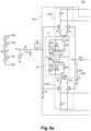
- the power supply circuit 151 comprises a MOSFET transistor M1, M2 directly connected to the first power supply bus V++ by its drain and to the second power supply bus V+ by its source via a fourth diode D3, D11, which can be a conventional diode or a Schottky diode.
- the anode of the fourth diode D3 is connected to the second power supply bus V+ and its cathode to the output signal numbered 2 representing the output signal of the power supply circuit 151-155, 155a, 155b ; the cathode of the fourth diode D11 is connected to the second power supply bus -V+.
- MOSFET transistor M1, M2 is blocked for a voltage lower than a threshold, typically 35 V, then switches and operates linearly beyond this threshold.
- MOSFET transistor M1, M2 passes the first power bus V++ when a control voltage greater than the threshold value is applied to it. This voltage is controlled by the combination of a charge assistance subcircuit 131, a discharge assistance subcircuit 141 and a voltage shift subcircuit 161.
- the charging assistance subcircuit 131 comprises a first resistor R24, R31 connected between the gate of the MOSFET transistor M1, M2 and an interconnection point A1, A2.
- the voltage shift subcircuit 161 comprises a first capacitor C18, C23 connected in parallel with a first diode D8, D10.
- the cathode of the first diode D8 is connected to a first interconnection node N1 and the anode of the first diode D8 is connected to a second interconnection node N2.
- the diode D10 is connected in reverse, i.e., its cathode is connected to the interconnection node N3 and its anode is connected to the interconnection node N4, as illustrated in the Figure 5a-5b
- the first interconnection node is connected to interconnection point A1 and the second interconnection node is connected to loudspeaker R44.
- the voltage shift sub-circuit ensures that the gate potential of MOSFET transistor M1 is always 15 V higher than that of the amplifier output.
- the Darlington circuit consisting of transistors Q8 and Q10 requires a 5 V dropout voltage, i.e., the voltage equal to the difference between the input voltage on the collector of transistor Q8 and the output voltage of the emitter of transistor Q10.
- MOSFET M1 on the other hand, requires a 10 V dropout voltage; i.e., the voltage equal to the difference between the input voltage on its gate and the output voltage on its source in the case where the current is maximum and saturated.
- the power supply circuit 151 advantageously comprises a first protection diode D5, D13.
- the anode of the diode D5 is connected to the output signal 2 of the power supply circuit 151 and its cathode is connected to the gate of the MOSFET transistor M1.
- the cathode of the diode D13 is connected to the output of the power supply circuit 155b and its anode is connected to the gate of the MOSFET transistor M2.
- the power supply circuit 151 comprises a second protection diode D4, D12.
- the cathode of the diode D4 is connected to the drain of the MOSFET transistor M1 and its anode is connected to the source of the MOSFET transistor M1.
- the cathode of the diode D12 is connected to the source of the MOSFET transistor M2 and its anode is connected to the drain of the MOSFET transistor M2.
- the signals illustrated on the Figure 7 correspond to the signals obtained with a 20kHz sinusoid supplied at the input of the high-power amplifier 102.
- the output signal 3 is distorted at the peaks of the sinusoids which take on a triangular appearance.
- the signals illustrated on the figure 8 correspond to the signals obtained with a 1kHz sinusoid supplied at the input of the high-power amplifier 102.
- TDD harmonic distortion rate
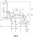
- the voltage shift sub-circuit 162 of the power supply stage 152 further comprises a second diode D6, D29 connected in parallel with a fourth resistor R22, R26.
- the cathode of the second diode D6 is connected to the interconnection point N1 and the anode of the second diode D6 is connected to the third interconnection node N10.
- the diode D29 is connected in the opposite direction, i.e. its cathode is connected to the interconnection node N20 and its anode is connected to the interconnection node N4, as illustrated in the Figure 5a-5b .
- the signals illustrated on the Figure 10 correspond to the signals obtained with a 20kHz sinusoid supplied at the input of the high-power amplifier 102. It is still observed that the output signal 3 is distorted at the peaks of the sinusoids, which take on a triangular appearance. Thus, it is still not possible to correctly reproduce a 20 kHz sinusoid.
- the signals illustrated on the Figure 11 correspond to the signals obtained with a 1kHz frequency sinusoid supplied at the input of the high-power amplifier 102.
- the sinusoid of the output signal 3 seems perfectly reproduced on the positive alternation and slightly distorted on the negative alternation.
- the distortion by harmonics THD is equal to 0.45% because the observed deformation corresponds to the production of harmonics.
- Adding these components therefore does not reduce the distortions observed on the amplifier's output signal.
- Adding the second diode D6, D29 and the fourth resistor R22, R26 degrades the dynamic performance of the circuit. More complex circuitry is required for these components to be beneficial, i.e., to improve degradation at low and high frequencies. To achieve a performance gain, it is possible to add other elements around transistor Q12, Q13.
- the charging assistance sub-circuit 132 of the power supply stage 153 further comprises a circuit branch comprising a third diode D9, D14 in series with a fifth resistor R29, R30, connected in parallel with the first resistor R24, R31.
- the cathode of the third diode D9 is for example connected to the gate of the MOSFET transistor M1.
- the anode of the third diode D14 is connected to the gate of the MOSFET transistor M2.
- the components D9, R29 and D14, R30 can be reversed, such that the third diode D9, D14 is connected to the gate of the MOSFET transistor M1, M2 via the resistor R29, R30.
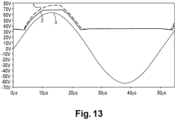
- the different signals obtained are illustrated on the Figure 13 . These correspond to the signals obtained with a 20kHz frequency sinusoid supplied at the input of the high-power amplifier 102.
- the output sinusoid corresponding to the output signal numbered 3 is well restored.
- the output signal 2 representing the output voltage of the power supply circuit 153, presents distortions between 0 and 5 ⁇ s and between 18 and 20 ⁇ s.
- the THD rate is equal to 0.26%.
- the addition of these components here makes it possible to improve the distortion for an input sinusoidal signal up to a frequency of 20kHz.
- the voltage shift sub-circuit of the power supply stage 154 further comprises a third capacitor C21, C24 connected in parallel with the fourth resistor R22, R26 and the second diode D6, D29, as well as a second capacitor C17, C22, connected in parallel with the first diode D8, D10 and the first capacitor C18, C23.
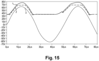
- the different signals obtained are illustrated on the Figure 15 . These correspond to the signals obtained with a 20kHz frequency sinusoid supplied at the input of the high-power amplifier 102.
- the second capacitor C17, C22 for example using electrochemical technology, has a high value, typically between 5 and 15 ⁇ F, constitutes an energy reservoir, while the first capacitor C18, C23, for example using plastic film technology, has a lower value, typically between 50 and 150nF, allows to smooth out high-frequency interference.
- the THD is reduced to 0.21%
- the power supply stage 155, 155a, 155b further comprises a fourth capacitor C14, C25 connected in parallel with the fourth diode D3, D11.
- the different signals obtained are illustrated on the Figure 17 . These correspond to the signals obtained with a 20kHz frequency sinusoid supplied at the input of the high-power amplifier 102.
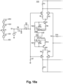
- a current measuring resistor R61 is inserted between the loudspeaker R44 and ground.
- the current amplifier 103 does not have a protection line 403.
- the bases of the transistors Q2 and Q4 are connected to an interconnection point located between the resistor R61 and the loudspeaker R44 via a capacitor C40. This capacitor C40 therefore only allows the alternating component of the signal to pass.
- the loudspeaker R44 is therefore crossed by an alternating current, an image of which is applied to point S2. It follows that the transconductance of the amplifier is equal to 1/R61 for an alternating signal.
- a resistor can be added to the feedback, between point S2 and the output of amplifier 3.
- the DC component is applied to the bases of transistors Q2 and Q4 via a resistor R18.
- the feedback will tend to cancel this DC component.
- resistor R18 limits the gain of the amplifier in the absence of speaker R44, also preventing it from oscillating.
- capacitor C40 has a negligible impedance compared to the value of resistor R18. In normal operation, that is, when there is no DC component and when a speaker R44 is actually present at the amplifier output, resistor R18 has almost no effect.
- the capacitor behaves like an open circuit, the DC component is thus reinjected at point S2 via resistor R18.
- the voltage gain is thus limited to 1 for DC voltages, which does not risk damaging loudspeaker R44.
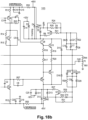
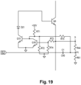
- a current amplifier protection circuit can be added.
- the interconnection point P1 located between the resistor R61 and the loudspeaker R44 is connected to a first terminal of a resistor R70.
- the second terminal of the resistor R70 is connected to the collector of a transistor Q16.
- the collector of the transistor Q16 is also connected to the base of a second transistor Q15.
- the voltage divider formed by the resistors R71 and R72 makes it possible to adapt the current threshold from which the protection circuit acts.
- the first terminal of the resistor R71 is connected to the second power supply bus V+ with a value of 32 V.
- transistor Q15 is a Darlington. This limits the distortion due to the circuit by drawing a lower current from the terminals of the measuring resistor R61 while maintaining sufficient sensitivity thanks to the divider network R71 / R72.
- Another divider bridge consisting of resistors R73 and R74 is inserted between point 3 and ground. The first terminal of resistor R73 is connected to point 3. The second terminal of resistor R73 is connected to the base of transistor Q16 and to the first terminal of resistor R74. The second terminal of the latter is connected to ground. This adapts the voltage threshold from which the current protection is neutralized.
- the emitters of transistors Q16 and Q15 are connected to each other and to ground, and the collector of transistor Q15 is connected to the base of transistor Q8 via a diode D21, whose cathode is connected to the collector of transistor Q15.
- This circuit must be mirrored to manage the current protection during the negative alternation, the NPN type transistors are then replaced by PNP type transistors.
- This circuit limits the risk of power failure of the amplifier under current, especially when it is overloaded or when its output is short-circuited. In these cases, the product of the output current by the voltage of the power supply buses will be entirely dissipated by the transistors and these could be damaged.
- the invention makes it possible to obtain a high-power audio amplifier making it possible to limit the distortions identified on the signals and therefore to improve the efficiency and reduce the saturation of the amplifier.
Landscapes
- Engineering & Computer Science (AREA)
- Power Engineering (AREA)
- Multimedia (AREA)
- Amplifiers (AREA)
Claims (10)
- Hochleistungsfähiger Audioverstärker (102) zur Steuerung mindestens eines Lautsprechers (R44), wobei der Verstärker Folgendes umfasst:- eine Vorverstärkerstufe (201, 301), die ein Eingangssignal (S1) empfängt;- eine Leistungsverstärkerstufe (202-203, 302), die mit der Vorverstärkerstufe (201, 301) verbunden ist und ein Ausgangssignal (3) zur Versorgung des mindestens einen Lautsprechers (R44) abgibt; wobei die Vorverstärkerstufen (201, 301) und die Leistungsverstärkerstufe (202-203, 302) einen oberen und einen unteren Teil aufweisen, die spiegelbildlich angeordnet sind;- eine Rückkopplung, die der Vorverstärkerstufe (201, 301) ein Abbild des Ausgangssignals (3) liefert;- eine obere Versorgungsschaltung (151-155, 155a), die mit dem oberen Teil der Leistungsverstärkerstufe (202-203, 302) verbunden ist und diesen über einen ersten oder zweiten Versorgungsbus (V++, V+) versorgt;- eine untere Versorgungsschaltung (155b), die mit dem unteren Teil der Leistungsverstärkerstufe (202-203, 302) verbunden ist und diesen über einen ersten oder zweiten Versorgungsbus versorgt;- jede Versorgungsschaltung (151-155, 155a, 155b) umfasst einen MOSFET-Transistor (M1, M2) und Überwachungsmittel, wobei der MOSFET-Transistor (M1, M2) von den Überwachungsmitteln so gesteuert wird, dass er zwischen dem einen oder dem anderen der beiden Versorgungsbusse (V++, V+) umschaltet,- dadurch gekennzeichnet, dass der MOSFET-Transistor (M1, M2) über eine vierte Diode (D3, D11) mit dem zweiten Versorgungsbus (V+) verbunden ist, deren erster Anschluss mit der Source des MOSFET-Transistors (M1, M2) verbunden ist, und der Drain des MOSFET-Transistors (M1, M2) mit dem ersten Versorgungsbus (V++) verbunden ist, wobei jede Versorgungsschaltung (151-155, 155a, 155b) ferner Folgendes umfasst:- eine Teilschaltung zur Lastunterstützung (131-133) des MOSFET-Transistors (M1, M2) mit mindestens einem ersten Widerstand (R24, R31), wobei ein erster Anschluss des ersten Widerstands (R24, R31) mit dem Gate des MOSFET-Transistors (M1, M2) verbunden ist und ein zweiter Anschluss des ersten Widerstands (R24, R31) mit einem Zwischenschaltungspunkt (A1) verbunden ist;- eine Teilschaltung zur Entladungsunterstützung (141) des MOSFET-Transistors (M1, M2), die mindestens einen zweiten und einen dritten Widerstand (R8, R27, R21, R39) und einen Bipolartransistor (Q12, Q13) umfasst; wobei die Basis des Bipolartransistors (Q12, Q13) mit einem ersten Anschluss des dritten Widerstands (R21, R39) verbunden ist, sein Emitter mit dem Gate des MOSFET-Transistors (M1, M2) verbunden ist, und sein Kollektor über den zweiten Widerstand (R8) mit der Source des MOSFET-Transistors (M1, M2) verbunden ist und der zweite Anschluss des dritten Widerstands (R21, R39) über den Zwischenschaltungspunkt (A1, A2) verbunden ist; und- eine Teilschaltung zur Spannungsschiebung (161-163) mit einer ersten Diode (D8, D10), die parallel zu einem ersten Kondensator (C18, C23) geschaltet ist; wobei ein erster Anschluss der ersten Diode (D8, D10) und ein erster Anschluss des ersten Kondensators (C8, C23) mit einem ersten Verbindungsknoten (N1, N4) verbunden sind, der seinerseits mit dem Zwischenschaltungspunkt (A1, A2) der Teilschaltung zur Entladungsunterstützung (141) verbunden ist; wobei ein zweiter Anschluss der ersten Diode (D8, D10) und ein zweiter Anschluss des ersten Kondensators (C18, C23) an einen zweiten Verbindungsknoten (N2, N3) angeschlossen sind, der seinerseits mit dem Ausgangssignal (3) verbunden ist.
- Verstärker nach Anspruch 1, dadurch gekennzeichnet, dass die Teilschaltung zur Spannungsverschiebung (161-163) ferner mindestens einen vierten Widerstand (R22, R26) und eine zweite Diode (D6, D29) aufweist, die parallel geschaltet sind, wobei ein erster Anschluss der zweiten Diode (D6, D29) und ein Anschluss des vierten Widerstands (R22, R26) mit dem Zwischenschaltungspunkt (A1, A2) verbunden sind und ein zweiter Anschluss des vierten Widerstands (R22, R26) und ein zweiter Anschluss der zweiten Diode (D6, D29) mit einem dritten Verbindungsknoten (N10) verbunden sind.
- Verstärker nach Anspruch 1 oder 2, dadurch gekennzeichnet, dass die Teilschaltung zur Lastunterstützung (131-133) außerdem einen fünften Widerstand (R29, R30) umfasst, der mit einer dritten Diode (D9, D14) in Reihe geschaltet ist, wobei der fünfte Widerstand (R29, R30) und die dritte Diode (D9, D14) parallel zum Zweig der Teilschaltung zur Lastunterstützung (131-133) geschaltet sind, der den ersten Widerstand (R24, R31) umfasst.
- Verstärker nach einem der Ansprüche 1 bis 3, dadurch gekennzeichnet, dass die Teilschaltung zur Spannungsverschiebung (161-163) ferner einen zweiten Kondensator (C17, C22) und einen dritten Kondensator (C21, C24) umfasst, wobei der zweite Kondensator (C17, C22) parallel zum ersten Kondensator (C18, C23) und zur ersten Diode (D8, D19) geschaltet ist und der dritte Kondensator (C21, C24) parallel zur zweiten Diode (D6, D29) und zum fünften Widerstand (R22, R26) geschaltet ist.
- Verstärker nach einem der Ansprüche 1 bis 4, dadurch gekennzeichnet, dass jede Versorgungsschaltung (151-155, 155a, 155b) eine erste Schutzdiode (D5, D13) aufweist, deren erster Anschluss mit der Source des MOSFET-Transistors (M1, M2) verbunden ist und deren zweiter Anschluss mit dem Gate des MOSFET-Transistors (M1, M2) verbunden ist.
- Verstärker nach einem der Ansprüche 1 bis 5, dadurch gekennzeichnet, dass jede Versorgungsschaltung (151-155, 155a, 155b) außerdem eine zweite Schutzdiode (D4, D12) aufweist, die zwischen der Source und dem Drain des MOSFET-Transistors (M1, M2) geschaltet ist.
- Verstärker nach einem der Ansprüche 1 bis 6, dadurch gekennzeichnet, dass jede Versorgungsschaltung (151-155, 155a, 155b) außerdem einen vierten Kondensator (C14, C25) enthält, der parallel zur vierten Diode (D3, D11) geschaltet ist.
- Verstärker nach einem der Ansprüche 1 bis 7, dadurch gekennzeichnet, dass die Vorverstärkerstufe (201, 301) über eine Schaltung zur Dämpfung von Leistungsschwankungen (304, 305) des ersten Versorgungsbusses (V++) mit dem ersten Versorgungsbus (V++) jeder Versorgungsschaltung (151-155, 155a, 155b) verbunden ist, wobei die Schaltung zur Dämpfung von Leistungsschwankungen (304, 305) mindestens einen Kondensator (C15, C19) und mindestens einen Widerstand (R52, R55) umfasst, die als Tiefpassfilter geschaltet sind.
- Verstärker nach Anspruch 8, dadurch gekennzeichnet, dass die Schaltung zur Dämpfung von Leistungsschwankungen (304, 305) außerdem einen zusätzlichen Kondensator enthält, der parallel zu dem mindestens einen Kondensator (C16, C20) geschaltet ist.
- Verstärker nach einem der Ansprüche 1 bis 9, dadurch gekennzeichnet, dass die Rückkopplung der Vorverstärkerstufe ein Signal abgibt, das proportional zum Strom ist, der durch den Lautsprecher fließt.
Applications Claiming Priority (2)
| Application Number | Priority Date | Filing Date | Title |
|---|---|---|---|
| FR2200839A FR3132399B1 (fr) | 2022-01-31 | 2022-01-31 | Amplificateur audio haute performance |
| PCT/EP2023/051797 WO2023144200A1 (fr) | 2022-01-31 | 2023-01-25 | Amplificateur audio haute performance |
Publications (3)
| Publication Number | Publication Date |
|---|---|
| EP4473658A1 EP4473658A1 (de) | 2024-12-11 |
| EP4473658C0 EP4473658C0 (de) | 2025-04-09 |
| EP4473658B1 true EP4473658B1 (de) | 2025-04-09 |
Family
ID=82019586
Family Applications (1)
| Application Number | Title | Priority Date | Filing Date |
|---|---|---|---|
| EP23701752.0A Active EP4473658B1 (de) | 2022-01-31 | 2023-01-25 | Hochleistungs-audioverstärker |
Country Status (7)
| Country | Link |
|---|---|
| US (1) | US12316287B1 (de) |
| EP (1) | EP4473658B1 (de) |
| JP (1) | JP7717986B2 (de) |
| KR (1) | KR102872576B1 (de) |
| CN (1) | CN118715711B (de) |
| FR (1) | FR3132399B1 (de) |
| WO (1) | WO2023144200A1 (de) |
Family Cites Families (12)
| Publication number | Priority date | Publication date | Assignee | Title |
|---|---|---|---|---|
| JPS50150346A (de) * | 1974-05-21 | 1975-12-02 | ||
| KR20000008691A (ko) * | 1998-07-15 | 2000-02-15 | 구자홍 | 음성보상 장치 |
| JP2001068986A (ja) * | 1999-08-30 | 2001-03-16 | Nec Ic Microcomput Syst Ltd | 半導体装置の出力バッファ回路 |
| JP2004214843A (ja) * | 2002-12-27 | 2004-07-29 | Alpine Electronics Inc | デジタルアンプ及びそのゲイン調整方法 |
| US9575715B2 (en) * | 2008-05-16 | 2017-02-21 | Adobe Systems Incorporated | Leveling audio signals |
| SG173836A1 (en) * | 2009-02-25 | 2011-09-29 | Thx Ltd | Low dissipation amplifier |
| US8049536B2 (en) * | 2009-11-30 | 2011-11-01 | Himax Technologies Limited | Half-power buffer amplifier |
| CN103138687B (zh) * | 2011-11-22 | 2017-04-12 | 应美盛股份有限公司 | 能处理高电平的音频放大电路中的失真抑制 |
| ITMI20121624A1 (it) * | 2012-09-28 | 2014-03-29 | St Microelectronics Srl | Amplificatore in classe "g" e sistema audio impiegante l'amplificatore |
| US10026375B2 (en) * | 2016-03-29 | 2018-07-17 | Himax Technologies Limited | Output amplifier of a source driver and control method thereof |
| JP7334977B2 (ja) * | 2017-04-28 | 2023-08-29 | ブルメスター オーディオシステム ゲーエムベーハー | 信号増幅器回路、電圧変換器およびシステム |
| US12334950B2 (en) * | 2022-12-28 | 2025-06-17 | Texas Instruments Incorporated | Dynamic range boost for amplifiers |
-
2022
- 2022-01-31 FR FR2200839A patent/FR3132399B1/fr active Active
-
2023
- 2023-01-25 EP EP23701752.0A patent/EP4473658B1/de active Active
- 2023-01-25 WO PCT/EP2023/051797 patent/WO2023144200A1/fr not_active Ceased
- 2023-01-25 JP JP2024545191A patent/JP7717986B2/ja active Active
- 2023-01-25 KR KR1020247029301A patent/KR102872576B1/ko active Active
- 2023-01-25 US US18/834,318 patent/US12316287B1/en active Active
- 2023-01-25 CN CN202380019139.8A patent/CN118715711B/zh active Active
Also Published As
| Publication number | Publication date |
|---|---|
| US20250158584A1 (en) | 2025-05-15 |
| CN118715711B (zh) | 2025-08-22 |
| EP4473658C0 (de) | 2025-04-09 |
| JP2025503287A (ja) | 2025-01-30 |
| KR20240141205A (ko) | 2024-09-25 |
| JP7717986B2 (ja) | 2025-08-04 |
| WO2023144200A1 (fr) | 2023-08-03 |
| CN118715711A (zh) | 2024-09-27 |
| FR3132399B1 (fr) | 2025-07-25 |
| FR3132399A1 (fr) | 2023-08-04 |
| EP4473658A1 (de) | 2024-12-11 |
| KR102872576B1 (ko) | 2025-10-20 |
| US12316287B1 (en) | 2025-05-27 |
Similar Documents
| Publication | Publication Date | Title |
|---|---|---|
| FR2532806A1 (fr) | Dispositif servant a convertir un signal electrique en un signal acoustique | |
| FR2724072A1 (fr) | Etage amplificateur de puissance, de type suiveur. | |
| EP0135412A1 (de) | Geregelte Speiseschaltung für einen Telefonapparat | |
| EP4473658B1 (de) | Hochleistungs-audioverstärker | |
| EP0737003B1 (de) | Ausleseverstärker für CCD-Register | |
| HK40116348A (en) | High-performance audio amplifier | |
| FR2664445A1 (fr) | Circuit amplificateur differentiel a faible distorsion et procede d'utilisation. | |
| EP3206038B1 (de) | Vorrichtung zum messen eines elektrischen stroms, der von einem akustischen verstärker erzeugt wird, um eine lautsprecherbox zu aktivieren | |
| FR2582169A1 (fr) | Appareil amplificateur | |
| FR2873872A1 (fr) | Amplificateur audio classe ad | |
| FR2533779A1 (fr) | Amplificateur audiofrequence de puissance avec regulation automatique du courant de polarisation absorbe par l'etage final | |
| FR2581275A1 (fr) | Recepteur de signaux optiques a tres large bande. | |
| EP2514219A1 (de) | Gerät mit vorrichtung für den anschluss von einem oder mehreren aussenlautsprechern sowie mit vorrichtung zur erkennung eines derartigen anschlusses | |
| EP0083529A2 (de) | Verstärkereinrichtung für stark schwankende Spannungen und Spannungsquelle mit einer derartigen Verstärkereinrichtung | |
| FR2602379A1 (fr) | Circuit repeteur de tension pour charges a composante ohmique, avec compensation de la distorsion harmonique | |
| HK40116348B (zh) | 高性能音频放大器 | |
| FR2498844A1 (fr) | Dispositif de protection thermique d'un amplificateur de puissance en classe b, c, d ou ab et amplificateur comportant un tel dispositif | |
| EP0608938A1 (de) | Verstärker mit Differenzeingangsstufe und integrierter Stabilisierungskapazität | |
| FR3048315B1 (fr) | Convertisseur courant-tension, etage d'entree d'un amplificateur et amplificateur correspondant. | |
| FR2796222A1 (fr) | Amplificateur operationnel multi-etage a controle de stabilite | |
| FR2884984A1 (fr) | Dispositif d'amplification de puissance d'un signal audiophonique et systeme d'amplification symetrique utilisant un tel dispositif | |
| FR2768871A1 (fr) | Amplificateur de courant, en particulier pour ligne telephonique | |
| EP1414148B1 (de) | Leistungsverstärker für Hochfrequenz-Transmissionssysteme | |
| FR2841408A1 (fr) | Procede et dispositif pour la reception de signaux differentiels avec une forte rejection du mode commun | |
| EP0577474A1 (de) | Weckschaltung für einen Telefonapparat |
Legal Events
| Date | Code | Title | Description |
|---|---|---|---|
| STAA | Information on the status of an ep patent application or granted ep patent |
Free format text: STATUS: UNKNOWN |
|
| STAA | Information on the status of an ep patent application or granted ep patent |
Free format text: STATUS: THE INTERNATIONAL PUBLICATION HAS BEEN MADE |
|
| PUAI | Public reference made under article 153(3) epc to a published international application that has entered the european phase |
Free format text: ORIGINAL CODE: 0009012 |
|
| STAA | Information on the status of an ep patent application or granted ep patent |
Free format text: STATUS: REQUEST FOR EXAMINATION WAS MADE |
|
| 17P | Request for examination filed |
Effective date: 20240730 |
|
| AK | Designated contracting states |
Kind code of ref document: A1 Designated state(s): AL AT BE BG CH CY CZ DE DK EE ES FI FR GB GR HR HU IE IS IT LI LT LU LV MC ME MK MT NL NO PL PT RO RS SE SI SK SM TR |
|
| GRAP | Despatch of communication of intention to grant a patent |
Free format text: ORIGINAL CODE: EPIDOSNIGR1 |
|
| STAA | Information on the status of an ep patent application or granted ep patent |
Free format text: STATUS: GRANT OF PATENT IS INTENDED |
|
| DAV | Request for validation of the european patent (deleted) | ||
| DAX | Request for extension of the european patent (deleted) | ||
| INTG | Intention to grant announced |
Effective date: 20250109 |
|
| GRAS | Grant fee paid |
Free format text: ORIGINAL CODE: EPIDOSNIGR3 |
|
| GRAA | (expected) grant |
Free format text: ORIGINAL CODE: 0009210 |
|
| STAA | Information on the status of an ep patent application or granted ep patent |
Free format text: STATUS: THE PATENT HAS BEEN GRANTED |
|
| RAP3 | Party data changed (applicant data changed or rights of an application transferred) |
Owner name: FOCAL JMLAB |
|
| AK | Designated contracting states |
Kind code of ref document: B1 Designated state(s): AL AT BE BG CH CY CZ DE DK EE ES FI FR GB GR HR HU IE IS IT LI LT LU LV MC ME MK MT NL NO PL PT RO RS SE SI SK SM TR |
|
| REG | Reference to a national code |
Ref country code: GB Ref legal event code: FG4D Free format text: NOT ENGLISH |
|
| REG | Reference to a national code |
Ref country code: CH Ref legal event code: EP |
|
| REG | Reference to a national code |
Ref country code: HK Ref legal event code: DE Ref document number: 40116348 Country of ref document: HK |
|
| REG | Reference to a national code |
Ref country code: IE Ref legal event code: FG4D Free format text: LANGUAGE OF EP DOCUMENT: FRENCH |
|
| U01 | Request for unitary effect filed |
Effective date: 20250409 |
|
| U07 | Unitary effect registered |
Designated state(s): AT BE BG DE DK EE FI FR IT LT LU LV MT NL PT RO SE SI Effective date: 20250415 |
|
| PG25 | Lapsed in a contracting state [announced via postgrant information from national office to epo] |
Ref country code: ES Free format text: LAPSE BECAUSE OF FAILURE TO SUBMIT A TRANSLATION OF THE DESCRIPTION OR TO PAY THE FEE WITHIN THE PRESCRIBED TIME-LIMIT Effective date: 20250409 |
|
| PG25 | Lapsed in a contracting state [announced via postgrant information from national office to epo] |
Ref country code: GR Free format text: LAPSE BECAUSE OF FAILURE TO SUBMIT A TRANSLATION OF THE DESCRIPTION OR TO PAY THE FEE WITHIN THE PRESCRIBED TIME-LIMIT Effective date: 20250710 Ref country code: NO Free format text: LAPSE BECAUSE OF FAILURE TO SUBMIT A TRANSLATION OF THE DESCRIPTION OR TO PAY THE FEE WITHIN THE PRESCRIBED TIME-LIMIT Effective date: 20250709 |
|
| PG25 | Lapsed in a contracting state [announced via postgrant information from national office to epo] |
Ref country code: PL Free format text: LAPSE BECAUSE OF FAILURE TO SUBMIT A TRANSLATION OF THE DESCRIPTION OR TO PAY THE FEE WITHIN THE PRESCRIBED TIME-LIMIT Effective date: 20250409 |
|
| PG25 | Lapsed in a contracting state [announced via postgrant information from national office to epo] |
Ref country code: HR Free format text: LAPSE BECAUSE OF FAILURE TO SUBMIT A TRANSLATION OF THE DESCRIPTION OR TO PAY THE FEE WITHIN THE PRESCRIBED TIME-LIMIT Effective date: 20250409 |
|
| PG25 | Lapsed in a contracting state [announced via postgrant information from national office to epo] |
Ref country code: RS Free format text: LAPSE BECAUSE OF FAILURE TO SUBMIT A TRANSLATION OF THE DESCRIPTION OR TO PAY THE FEE WITHIN THE PRESCRIBED TIME-LIMIT Effective date: 20250709 |
|
| PG25 | Lapsed in a contracting state [announced via postgrant information from national office to epo] |
Ref country code: IS Free format text: LAPSE BECAUSE OF FAILURE TO SUBMIT A TRANSLATION OF THE DESCRIPTION OR TO PAY THE FEE WITHIN THE PRESCRIBED TIME-LIMIT Effective date: 20250809 |
|
| PG25 | Lapsed in a contracting state [announced via postgrant information from national office to epo] |
Ref country code: SM Free format text: LAPSE BECAUSE OF FAILURE TO SUBMIT A TRANSLATION OF THE DESCRIPTION OR TO PAY THE FEE WITHIN THE PRESCRIBED TIME-LIMIT Effective date: 20250409 |
|
| PG25 | Lapsed in a contracting state [announced via postgrant information from national office to epo] |
Ref country code: CZ Free format text: LAPSE BECAUSE OF FAILURE TO SUBMIT A TRANSLATION OF THE DESCRIPTION OR TO PAY THE FEE WITHIN THE PRESCRIBED TIME-LIMIT Effective date: 20250409 |
|
| PG25 | Lapsed in a contracting state [announced via postgrant information from national office to epo] |
Ref country code: SK Free format text: LAPSE BECAUSE OF FAILURE TO SUBMIT A TRANSLATION OF THE DESCRIPTION OR TO PAY THE FEE WITHIN THE PRESCRIBED TIME-LIMIT Effective date: 20250409 |
|
| REG | Reference to a national code |
Ref country code: CH Ref legal event code: U11 Free format text: ST27 STATUS EVENT CODE: U-0-0-U10-U11 (AS PROVIDED BY THE NATIONAL OFFICE) Effective date: 20260201 |
|
| PLBE | No opposition filed within time limit |
Free format text: ORIGINAL CODE: 0009261 |
|
| STAA | Information on the status of an ep patent application or granted ep patent |
Free format text: STATUS: NO OPPOSITION FILED WITHIN TIME LIMIT |
|
| REG | Reference to a national code |
Ref country code: CH Ref legal event code: L10 Free format text: ST27 STATUS EVENT CODE: U-0-0-L10-L00 (AS PROVIDED BY THE NATIONAL OFFICE) Effective date: 20260218 |
|
| U20 | Renewal fee for the european patent with unitary effect paid |
Year of fee payment: 4 Effective date: 20260127 |
|
| 26N | No opposition filed |
Effective date: 20260112 |
|
| PGFP | Annual fee paid to national office [announced via postgrant information from national office to epo] |
Ref country code: CH Payment date: 20260201 Year of fee payment: 4 |