EP4471864A1 - Display device using light-emitting element and manufacturing method thereof - Google Patents
Display device using light-emitting element and manufacturing method thereof Download PDFInfo
- Publication number
- EP4471864A1 EP4471864A1 EP22926188.8A EP22926188A EP4471864A1 EP 4471864 A1 EP4471864 A1 EP 4471864A1 EP 22926188 A EP22926188 A EP 22926188A EP 4471864 A1 EP4471864 A1 EP 4471864A1
- Authority
- EP
- European Patent Office
- Prior art keywords
- layer
- light emitting
- display device
- insulating layer
- emitting device
- Prior art date
- Legal status (The legal status is an assumption and is not a legal conclusion. Google has not performed a legal analysis and makes no representation as to the accuracy of the status listed.)
- Pending
Links
Images






Classifications
-
- H—ELECTRICITY
- H10—SEMICONDUCTOR DEVICES; ELECTRIC SOLID-STATE DEVICES NOT OTHERWISE PROVIDED FOR
- H10H—INORGANIC LIGHT-EMITTING SEMICONDUCTOR DEVICES HAVING POTENTIAL BARRIERS
- H10H29/00—Integrated devices, or assemblies of multiple devices, comprising at least one light-emitting semiconductor element covered by group H10H20/00
- H10H29/80—Constructional details
- H10H29/85—Packages
- H10H29/855—Optical field-shaping means, e.g. lenses
- H10H29/8552—Light absorbing arrangements, e.g. black matrix
-
- H—ELECTRICITY
- H10—SEMICONDUCTOR DEVICES; ELECTRIC SOLID-STATE DEVICES NOT OTHERWISE PROVIDED FOR
- H10H—INORGANIC LIGHT-EMITTING SEMICONDUCTOR DEVICES HAVING POTENTIAL BARRIERS
- H10H20/00—Individual inorganic light-emitting semiconductor devices having potential barriers, e.g. light-emitting diodes [LED]
- H10H20/80—Constructional details
- H10H20/81—Bodies
- H10H20/813—Bodies having a plurality of light-emitting regions, e.g. multi-junction LEDs or light-emitting devices having photoluminescent regions within the bodies
- H10H20/8131—Stacked light-emitting regions
-
- H—ELECTRICITY
- H10—SEMICONDUCTOR DEVICES; ELECTRIC SOLID-STATE DEVICES NOT OTHERWISE PROVIDED FOR
- H10H—INORGANIC LIGHT-EMITTING SEMICONDUCTOR DEVICES HAVING POTENTIAL BARRIERS
- H10H29/00—Integrated devices, or assemblies of multiple devices, comprising at least one light-emitting semiconductor element covered by group H10H20/00
- H10H29/01—Manufacture or treatment
- H10H29/012—Manufacture or treatment of active-matrix LED displays
-
- H—ELECTRICITY
- H10—SEMICONDUCTOR DEVICES; ELECTRIC SOLID-STATE DEVICES NOT OTHERWISE PROVIDED FOR
- H10H—INORGANIC LIGHT-EMITTING SEMICONDUCTOR DEVICES HAVING POTENTIAL BARRIERS
- H10H29/00—Integrated devices, or assemblies of multiple devices, comprising at least one light-emitting semiconductor element covered by group H10H20/00
- H10H29/01—Manufacture or treatment
- H10H29/036—Manufacture or treatment of packages
- H10H29/0363—Manufacture or treatment of packages of optical field-shaping means
-
- H—ELECTRICITY
- H10—SEMICONDUCTOR DEVICES; ELECTRIC SOLID-STATE DEVICES NOT OTHERWISE PROVIDED FOR
- H10H—INORGANIC LIGHT-EMITTING SEMICONDUCTOR DEVICES HAVING POTENTIAL BARRIERS
- H10H29/00—Integrated devices, or assemblies of multiple devices, comprising at least one light-emitting semiconductor element covered by group H10H20/00
- H10H29/80—Constructional details
- H10H29/85—Packages
- H10H29/852—Encapsulations
- H10H29/854—Encapsulations characterised by their material, e.g. epoxy or silicone resins
-
- H—ELECTRICITY
- H10—SEMICONDUCTOR DEVICES; ELECTRIC SOLID-STATE DEVICES NOT OTHERWISE PROVIDED FOR
- H10H—INORGANIC LIGHT-EMITTING SEMICONDUCTOR DEVICES HAVING POTENTIAL BARRIERS
- H10H20/00—Individual inorganic light-emitting semiconductor devices having potential barriers, e.g. light-emitting diodes [LED]
- H10H20/01—Manufacture or treatment
- H10H20/036—Manufacture or treatment of packages
- H10H20/0362—Manufacture or treatment of packages of encapsulations
-
- H—ELECTRICITY
- H10—SEMICONDUCTOR DEVICES; ELECTRIC SOLID-STATE DEVICES NOT OTHERWISE PROVIDED FOR
- H10H—INORGANIC LIGHT-EMITTING SEMICONDUCTOR DEVICES HAVING POTENTIAL BARRIERS
- H10H20/00—Individual inorganic light-emitting semiconductor devices having potential barriers, e.g. light-emitting diodes [LED]
- H10H20/80—Constructional details
- H10H20/85—Packages
- H10H20/852—Encapsulations
- H10H20/854—Encapsulations characterised by their material, e.g. epoxy or silicone resins
-
- H—ELECTRICITY
- H10—SEMICONDUCTOR DEVICES; ELECTRIC SOLID-STATE DEVICES NOT OTHERWISE PROVIDED FOR
- H10H—INORGANIC LIGHT-EMITTING SEMICONDUCTOR DEVICES HAVING POTENTIAL BARRIERS
- H10H20/00—Individual inorganic light-emitting semiconductor devices having potential barriers, e.g. light-emitting diodes [LED]
- H10H20/80—Constructional details
- H10H20/85—Packages
- H10H20/855—Optical field-shaping means, e.g. lenses
-
- H—ELECTRICITY
- H10—SEMICONDUCTOR DEVICES; ELECTRIC SOLID-STATE DEVICES NOT OTHERWISE PROVIDED FOR
- H10H—INORGANIC LIGHT-EMITTING SEMICONDUCTOR DEVICES HAVING POTENTIAL BARRIERS
- H10H20/00—Individual inorganic light-emitting semiconductor devices having potential barriers, e.g. light-emitting diodes [LED]
- H10H20/80—Constructional details
- H10H20/882—Scattering means
-
- H—ELECTRICITY
- H10—SEMICONDUCTOR DEVICES; ELECTRIC SOLID-STATE DEVICES NOT OTHERWISE PROVIDED FOR
- H10H—INORGANIC LIGHT-EMITTING SEMICONDUCTOR DEVICES HAVING POTENTIAL BARRIERS
- H10H29/00—Integrated devices, or assemblies of multiple devices, comprising at least one light-emitting semiconductor element covered by group H10H20/00
- H10H29/01—Manufacture or treatment
- H10H29/036—Manufacture or treatment of packages
- H10H29/0362—Manufacture or treatment of packages of encapsulations
Definitions
- the present disclosure is applicable to a technical field related to a display device and relates to a display device using a Light Emitting Diode (LED) and a method of fabricating the same.
- LED Light Emitting Diode
- LCD Liquid Crystal Display
- PDP Plasma Display Panel
- ELD Electro Luminescent Display
- VFD Vacuum Fluorescent Display
- OLED Organic Light Emitting Diode
- Micro LED Micro Light Emitting Diode
- a digital signage is a display device that provides specific information as well as a broadcasting program in public places such as airport, hotel, hospital, and subway station, and the like, as a communication tool capable of inducing marketing, advertisement, training effects, and customer experience of enterprises as well as a general TV.
- a digital signage is a medium for displaying various contents and commercial advertisements by installing a display panel such as a Liquid Crystal Display (LCD), a Plasma Display Panel (PDP), an Organic Light Emitting Diode (OLED), a Micro LED Light Emitting Diode (LED), etc. in certain outdoor places or devices such as street furniture, and may be installed on public movement lines such as apartment elevators, subway stations, subway trains, buses, universities, banks, convenience stores, discount stores, and shopping malls, and the like.
- a display panel such as a Liquid Crystal Display (LCD), a Plasma Display Panel (PDP), an Organic Light Emitting Diode (OLED), a Micro LED Light Emitting Diode (LED), etc.
- LCD Liquid Crystal Display
- PDP Plasma Display Panel
- OLED Organic Light Emitting Diode
- LED Micro LED Light Emitting Diode
- Such digital signage is implemented as a modular display device in which various display modules are configured to be combined.
- a module display may use a Light Emitting Diode (LED) as a pixel.
- LED Light Emitting Diode
- a light emitting device When a light emitting device is used as a pixel (light source), when a black film is not applied to an upper side of the light emitting device, a central pixel area may be brightly represented but a periphery of the light source may not be represented sufficiently dark. This may be a phenomenon in which a sapphire used in the light emitting device has a large reflectivity with respect to an external incident light.
- the periphery of the light source may be represented to be sufficiently dark but the central white area may be darkened together by the application of the black film.
- contrast of a display may be reduced and a sufficient grayscale representation may be difficult.
- One technical task of the present disclosure is to provide a display device using a light emitting device and fabricating method thereof, by which light efficiency may be improved.
- Another technical task of the present disclosure is to provide a display device using a light emitting device and fabricating method thereof, by which a grayscale representation by a light source may be widely implemented.
- Another technical task of the present disclosure is to provide a stacked light emitting device and display device using the same, which may increase light efficiency by allowing light traveling to a side surface of a light emitting device to travel on a front surface,.
- Another technical task of the present disclosure is to provide a stacked light emitting device and display device using the same, which may uniformize a viewing angle due to different light distribution characteristics among red, green, and blue.
- Another technical task of the present disclosure is to provide a stacked light emitting device and display device using the same, which may improve a phenomenon in which a bright line occurs between modules when the display device has module structures connected to each other.
- a display device including a wiring substrate, a light emitting device disposed as an individual pixel on the wiring substrate, an insulating layer positioned on at least a side surface of the light emitting device, and a black layer positioned on the insulating layer, wherein the black layer may include a material formed by transforming a material forming the insulating layer.
- the black layer may include a material formed by carbonizing particles included in the insulating layer.
- the black layer may include a material formed by decomposing particles included in the insulating layer by heat.
- the material decomposed by the heat may include non-crystalline carbon and amorphous powder.
- the black layer may have a predetermined thickness on the insulating layer.
- the insulating layer may act as a reflective layer.
- the insulating layer may include a transparent resin layer and particles dispersed in the transparent resin layer.
- the transparent resin layer may include at least one of silicon, epoxy, or urethane.
- the particle may include at least one of silicon oxide, titanium oxide, or zirconium oxide.
- a refractive index of the particle may be different from that of the transparent resin layer.
- the light emitting device may include a semiconductor structure having a plurality of semiconductor layers stacked to emit light of a first color, a second color, and a third color.
- the light emitting device may include a support layer on the semiconductor structure.
- the insulating layer may be positioned to further surround a side surface of the support layer.
- the black layer may be positioned to surround at least a portion of a side surface of the support layer.
- a method of fabricating a display device using a light emitting device including disposing a plurality of light emitting devices forming individual pixels on a wiring substrate, forming an insulating layer including particles dispersed in a transparent resin layer between the light emitting devices, and forming a black layer by applying heat to the insulating layer.
- the applying the heat to the insulating layer may be performed by laser irradiation.
- the forming the black layer may include thermally decomposing particles included in the insulating layer by applying the heat.
- a lens may be positioned on the light emitting device so as not to react to the laser irradiation.
- a light source (light emitting device) side may be represented bright sufficiently, and a periphery of the light source may be represented sufficiently dark. Accordingly, a grayscale representation by the light source may be widely implemented.
- a black layer is not positioned on a light emitting device, an overall brightness of a display device may be improved.
- the light traveling to a side surface of a light emitting device is allowed to travel to a front surface, thereby increasing light efficiency.
- viewing angles due to different light distribution characteristics among red, green, and blue may be uniformized.
- a size of a light emitting device may be substantially expanded.
- a display device described in the present specification is a concept including all display devices displaying information as a unit pixel or a set of unit pixels. Therefore, the present disclosure is not limited to a finished product and may be applicable to a component.
- a panel corresponding to one component of a digital TV may also independently correspond to a display device of the present specification.
- the finished product may include a mobile phone, a smart phone, a laptop computer, a digital broadcasting terminal, Personal Digital Assistants (PDA), a Portable Multimedia Player (PMP), a navigation, a slate PC, a tablet PC, an Ultra Book, a digital TV, a desktop computer, etc.
- PDA Personal Digital Assistants
- PMP Portable Multimedia Player
- the semiconductor light emitting device mentioned in this specification is a concept including an LED, a micro LED, and the like, which may be used in a mixed manner.
- FIG. 1 is a cross-sectional diagram illustrating pixel regions of a display device using a light emitting device according to an embodiment of the present disclosure.
- FIG. 2 is a cross-sectional diagram illustrating a unit pixel region of a display device using a light emitting device according to an embodiment of the present disclosure.
- FIG. 3 is an enlarged diagram illustrating a display device using a light emitting device according to an embodiment of the present disclosure.
- light emitting devices 200 that form a plurality of pixels may be arranged on a wiring substrate 100 including a base substrate 120 provided with a wiring electrode 110.
- an insulating layer 300 may be disposed between a plurality of the light emitting devices 200.
- the insulating layer 300 may be disposed on at least a side surface of the light emitting device 200 to surround the side surface of the light emitting device 200.
- the insulating layer 300 may be provided to fill a space between the light emitting devices 200.
- a black layer 310 may be disposed on the insulating layer 300.
- the black layer 310 may serve as a black matrix layer that improves contrast of the display device 10.
- the black layer 310 may include a material formed by transforming a material forming the insulating layer 300.
- the black layer 310 may include a material formed by carbonizing particles included in the insulating layer 300.
- the black layer 310 may include a material in which particles included in the insulating layer 300 are decomposed by heat.
- the material decomposed by the heat may include non-crystalline carbon.
- the black layer 310 may be formed by carbonization of a resin included in the insulating layer 300.
- This carbonization phenomenon may be a phenomenon in which an organic material is pyrolyzed under appropriate conditions to generate non-crystalline carbon-black amorphous micropowder (soot). This will be described in detail later.
- the black layer 310 may have a predetermined thickness on the insulating layer 300. However, depending on embodiments, the thickness of the black layer 310 may vary depending on a distance between the light emitting devices 200.
- the insulating layer 300 may serve as a reflective layer. That is, the insulating layer 300 may serve as a reflective layer that reflects light emitted from the light emitting device 200 to the side surface. Meanwhile, the insulating layer 300 may insulate a first electrode 250 and a second electrode 260 of the light emitting device 200. In addition, the insulating layer 300 may act as a layer that fills a space between the light emitting devices 200 to planarize.
- the insulating layer 300 and the reflective layer 300 may be interchangeably described, and will be described using the same reference number.
- the insulating layer 300 may include particles 303 dispersed in a transparent resin layer 302.
- the particles 303 may act as reflective particles. This will be described in detail later.
- the wiring electrode 110 is briefly illustrated.
- a plurality of wiring electrodes 110 may be divided and positioned on the wiring substrate 110.
- the wiring electrode 110 may include a data electrode (pixel electrode) and a scan electrode (common electrode).
- the wiring electrode 110 arranged on the wiring substrate 100 may be connected to a TFT layer provided with a Thin Film Transistor (TFT).
- TFT Thin Film Transistor
- the data electrode (pixel electrode) may be connected to the TFT layer. A detailed description thereof will be omitted.
- the insulating layer 300 may have a hang structure 301 between the light emitting devices 200 neighboring to each other. That is, a curved structure 301 which is concavely formed between the neighboring light emitting devices 200 and continuously extends may be formed on a top surface of the insulating layer 300.
- a maximum height of the light emitting device 200 and a minimum height of the insulating layer 300 may be different from each other.
- the minimum height of the insulating layer 300 may be lower than the maximum height of the light emitting device 200.
- the height of the hang structure 301 may be higher than half of the height of the light emitting device 200.
- the hang structure 301 may be associated with a fabricating process of the insulating layer 300. For example, when the insulating layer 300 is formed using a jetting process of coating a material using a nozzle and then curing the material, the hang structure 301 may be formed.
- the light emitting device 200 may be disposed on the wiring substrate 100 while forming an individual pixel.
- a single light emitting device 200 may be configured to form a single pixel. Since the insulating layer 300 surrounding at least a side surface of the single light emitting device 200 constituting the individual pixel and acting as a reflective layer is formed, light emitted from the light emitting device 200 may be emitted upward without being mixed with light emitted from another light emitting device 200 constituting a neighboring pixel.
- the light emitted laterally from the individual light emitting devices 200 may be reflected by the insulating layer 300 and emitted toward an upper side of the display device 10.
- the light emitting device 200 constituting the individual pixel may include a semiconductor structure 202 including a plurality of semiconductor layers 210, 220, and 230 stacked to emit light of a first color, a second color, and a third color.
- the light emitting device 200 may be a stacked semiconductor light emitting device capable of emitting red, green, and blue light.
- the stacked light emitting device 200 may include a semiconductor structure 202 including a first semiconductor layer 210 emitting red light, a second semiconductor layer 220 emitting blue light, and a third semiconductor layer 230 emitting green light.
- the first semiconductor layer 210, the second semiconductor layer 220, and the third semiconductor layer 230 may include semiconductor layers capable of emitting lights of individual colors, respectively.
- each of the first semiconductor layer 210, the second semiconductor layer 220, and the third semiconductor layer 230 may include an active layer capable of emitting light of an individual color.
- each of the first semiconductor layer 210, the second semiconductor layer 220, and the third semiconductor layer 230 may include a n-type semiconductor layer and a p-type semiconductor layer together with an active layer capable of emitting light of an individual color. Such an individual structure is omitted from FIG. 2 .
- the light emitting device 200 may include a first electrode 250 and a second electrode 260 electrically connected to one side and the other side of the semiconductor structure, respectively.
- a first electrode 250 and a second electrode 260 electrically connected to one side and the other side of the semiconductor structure, respectively.
- FIG. 2 an electrical connection structure of the semiconductor structure, the first electrode 250, and the second electrode 260 is briefly illustrated.
- a support layer 240 may be disposed on the semiconductor structure 202.
- the support layer 240 may be a growth substrate in which the semiconductor structure 202 is grown or a transfer substrate in which the semiconductor structure 202 is transferred and bonded.
- the support layer 240 may be transparent to light emitted from the semiconductor structure 202.
- the support layer 240 may include a sapphire substrate.
- a lens 350 may be disposed on the support layer 240.
- the lens 350 does not react in the process of forming the black layer 310 so that the light emitting device 200 is allowed not to react with heat.
- first electrode 250 and the second electrode 260 which are electrically connected to one side and the other side of the semiconductor structure 202, respectively, may be provided with extension pads 251 and 261, respectively.
- a size of each of the extension pads 251 and 261 may become greater than an outer surface of the semiconductor structure 202.
- the light emitting device 200 as a light source will be described later in detail.
- the insulating layer 300 acts as a reflective layer and may be positioned to surround at least the side surface of the semiconductor structure 202 including the first semiconductor layer 210, the second semiconductor layer 220, and the third semiconductor layer 230 of the light emitting device 200.
- the insulating layer 300 may be positioned to cover the first electrode 250 and the second electrode 260. In addition, for example, the insulating layer 300 may be positioned to cover the extension pads 251 and 261.
- the insulating layer 300 may be positioned to further surround a side surface of the support layer 240 of the light emitting device 200.
- the insulating layer 300 may be positioned to surround all surfaces except for a top surface of the support layer 240 of the light emitting device.
- the black layer 310 may have a predetermined thickness on the insulating layer 300. That is, a thickness 'a' of the black layer 310 at a portion close to the light emitting device 200 may be the same as a thickness 'a" of a portion of the black layer 310 relatively far from the light emitting device 200.
- the predetermined thickness is formed along the insulating layer 300 by the above-mentioned carbonization (or pyrolysis) process.
- the black layer 310 may be formed in a manner that a heat source for carbonization (or pyrolysis) penetrates into the insulating layer to a predetermined depth irrespective of a position.
- the insulating layer 300 may include particles 303 dispersed in the transparent resin layer 302. These particles 303 may act as reflective particles.
- a refractive index of the particle 303 may be different from that of the transparent resin layer 302.
- the particle 303 may include at least one of silicon, titanium, zirconium, or an oxide thereof, e.g., silicon oxide (SiO x ), titanium oxide (TiO x ), or zirconium oxide (ZrO x ).
- the transparent resin layer 302 may be formed of a resin material.
- the transparent resin layer 302 may include at least one of silicon, epoxy, and urethane.
- a thickness of the insulating layer 300 may be set to have a reflectivity of 90% or more by the transparent resin layer 302 and the particles 303.
- FIG. 4 is a cross-sectional diagram illustrating a light emitting device of a display device using the light emitting device according to an embodiment of the present disclosure.
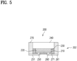
- FIG. 5 is a cross-sectional diagram illustrating a modified example of the light emitting device of FIG. 4 .
- a light emitting device 201 constituting an individual pixel may include a semiconductor structure 202 including a plurality of semiconductor layers 210, 220, and 230 stacked to emit light of a first color, a second color, and a third color.
- the light emitting device 201 may be a stacked semiconductor light emitting device capable of emitting red, green, and blue light.
- the stacked light emitting device 201 may include a semiconductor structure 202 including a first semiconductor layer 210 emitting red light, a second semiconductor layer 220 emitting blue light, and a third semiconductor layer 230 emitting green light.
- the first semiconductor layer 210, the second semiconductor layer 220, and the third semiconductor layer 230 may include semiconductor layers capable of emitting light of individual colors, respectively.
- each of the first semiconductor layer 210, the second semiconductor layer 220, and the third semiconductor layer 230 may include an active layer capable of emitting light of an individual color.
- each of the first semiconductor layer 210, the second semiconductor layer 220, and the third semiconductor layer 230 may include a n-type semiconductor layer and a p-type semiconductor layer together with an active layer capable of emitting light of an individual color.
- the light emitting device 201 may include a first electrode 250 and a second electrode 260 electrically connected to one side and the other side of the semiconductor structure 202, respectively.
- a support layer 240 may be disposed on the semiconductor structure 202.
- the support layer 240 may be a growth substrate in which the semiconductor structure 202 is grown or a transfer substrate in which the semiconductor structure 202 is transferred and bonded.
- a surface direction size of the support layer 240 may be greater than the semiconductor structure 202.
- a reflective layer 270 and 271 may be disposed on a side surface of the semiconductor structure 202 of the light emitting device 201.
- the reflective layer 270 and 271 may be positioned to surround the side surface of the semiconductor structure 202 including at least the first semiconductor layer 210, the second semiconductor layer 220, and the third semiconductor layer 230 of the light emitting device 200.
- the reflective layer 270 and 271 may be positioned to cover the first electrode 250 and the second electrode 260.
- the reflective layer 270 and 271 may be positioned to further surround the side surface of the support layer 240 of the light emitting device 201.
- the insulating layer 270 may be positioned to surround all surfaces except for a top surface of the support layer 240 of the light emitting device.
- the reflective layer may include a first reflective layer 271 covering side and bottom surfaces of the semiconductor structure including the first semiconductor layer 210, the second semiconductor layer 220, and the third semiconductor layer 230 and a second reflective layer 270 covering side surfaces of the first reflective layer 271 and the support layer 240.
- the reflective layer 270 and 271 may substantially extend a size of the light emitting device 201.
- a light emitting surface of the light emitting device 201 may be expanded to a size including the reflective layer 270 and 271. That is, the light emitting surface having an area corresponding to the semiconductor structure may be expanded to a size including the reflective layers 270 and 271.
- extension pads 251 and 261 respectively connected to the first electrode 250 and the second electrode 260 may be further provided.
- a size of the extension pad 251/261 may become greater over an outer surface of the semiconductor structure 202.
- the size of the extension pad 251/261 may be extended to an outer surface of the reflective layer 270.
- top surfaces of the extension pads 251 and 261 may be in contact with the reflective layer 270 and 271.
- the extension pad 251/261 may further improve the reflectivity of the reflective layer 270/271.
- the extension pad 251/261 may form a substantially external electrode pad of the light emitting device 201.
- the reflective layer 270 and 271 may include particles 303 dispersed in the transparent resin layer 302. That is, the characteristics of the reflective layer 270 and 271 of the present embodiment may be substantially the same as those of the reflective layer 300 described above. In other words, the characteristics of the reflective layer 270 and 271 of the present embodiment except for the characteristics having the hang structure 301 may be the same as those of the reflective layer 300 described above. Therefore, redundant descriptions will be omitted.
- FIG. 6 is a cross-sectional diagram illustrating a light emitting device of a display device using the light emitting device according to another embodiment of the present disclosure.
- FIG. 7 is a cross-sectional diagram illustrating a modified example of the light emitting device of FIG. 6 .
- a light emitting device 201 constituting an individual pixel may include a semiconductor structure 202 including a plurality of semiconductor layers 210, 220, and 230 stacked to emit light of a first color, a second color, and a third color. Since the semiconductor structure 202 is the same as that described with reference to FIG. 4 , a redundant description thereof will be omitted.
- the light emitting device 201 may include a first electrode 250 and a second electrode 260 electrically connected to one side and the other side of the semiconductor structure 202, respectively.
- a support layer 240 may be disposed on the semiconductor structure 202.
- the support layer 240 may be a growth substrate in which the semiconductor structure 202 is grown or a transfer substrate in which the semiconductor structure 202 is transferred and bonded.
- a surface direction size of the support layer 240 may be greater than the semiconductor structure 202.
- a reflective layer 271 and 272 may be disposed on a side surface of the semiconductor structure 202 of the light emitting device 201.
- the reflective layer may include a first reflective layer 271 covering a side surface of the semiconductor structure 202 including the first semiconductor layer 210, the second semiconductor layer 220, and the third semiconductor layer 230 and side surfaces of the first electrode 250 and the second electrode 260 and a second reflective layer 272 covering side and top surfaces of the first reflective layer 271 and the support layer 240.
- the second reflective layer 272 may be positioned to surround the side and top surfaces of the support layer 240 of the light emitting device 201.
- the second reflective layer 272 may improve uniformity of light emitted from the light emitting device 201.
- the reflective layer 271 and 272 may substantially extend a size of the light emitting device 201.
- a light emitting surface of the light emitting device 201 may be expanded to a size including the reflective layer 271 and 272. That is, the light emitting surface having an area corresponding to the semiconductor structure 202 may be expanded to a size including the reflective layer 271 and 272.
- extension pads 251 and 261 respectively connected to the first electrode 250 and the second electrode 260 may be further provided.
- a size of the extension pads 251 and 261 may become greater over an outer surface of the semiconductor structure 202.
- the size of the extension pads 251 and 261 may be expanded to an outer surface of the reflective layer 272.
- top surfaces of the extension pads 251 and 261 may be in contact with the reflective layer 271 and 272.
- the extension pads 251 and 261 may further improve reflectivity of the reflective layer 271 and 272.
- the extension pad 251/261 may form a substantially external electrode pad of the light emitting device 201.
- the reflective layer 271/272 may include particles 303 dispersed in the transparent resin layer 302. That is, the characteristics of the reflective layer 271/272 of the present embodiment may be substantially the same as those of the reflective layer 300 described above. In other words, the characteristics of the reflective layer 271/272 of the present embodiment except for the characteristics having the hang structure 301 may be the same as those of the reflective layer 300 described above. Therefore, redundant descriptions will be omitted.
- FIG. 8 is a cross-sectional diagram illustrating a display device using a light emitting device according to another embodiment of the present disclosure.
- FIG. 8 an embodiment of the display device 10 in which the light emitting device 201 according to the embodiment of FIG. 4 forms an individual pixel is illustrated.
- the light emitting device 201 may be installed on a wiring substrate 100 to form an individual pixel.
- a gap layer 400 may filled a space between the individual light emitting devices 201.
- the display device 10 may be implemented in a simple structure by using the light emitting device 201 having the structure expanded by a reflective layer 270, 271, and 272.
- a module display device 10 having a predetermined number of light emitting devices 201 may be implemented on the wiring substrate 100 having a predetermined size.
- the display device 10 having a desired size may be fabricated by combining the module display device 10.
- FIG. 9 is a schematic cross-sectional diagram illustrating a process of fabricating a display device using a light emitting device according to an embodiment of the present disclosure.
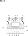
- FIG. 10 is a schematic diagram illustrating a partial region of FIG. 9 .
- FIG. 11 is a flowchart illustrating a process of fabricating a display device using a light emitting device according to an embodiment of the present disclosure.
- a process of forming a black layer 310 is schematically illustrated.
- a step S10 of disposing a plurality of light emitting devices 200 forming individual pixels on a wiring substrate 100 may be performed.
- a step S20 of forming an insulating layer 300 including particles 303 dispersed in a transparent resin layer 302 between the light emitting devices 200 may be performed.
- a step S30 of forming a black layer 310 by applying heat to the insulating layer 300 may be performed.
- FIG. 9 and FIG. 10 mainly illustrate the step S30 of forming the black layer 310 by applying heat to the insulating layer 300.
- the step of applying heat to the insulating layer 300 may be performed by laser irradiation.
- the black layer 310 may be formed by thermally decomposing the particles 303 included in the insulating layer 300 in a manner of applying heat to the insulating layer 300 by the laser irradiation.
- the resin (resin) may be carbonized by a pyrolysis process of the particles 303 or the transparent resin layer 302.
- Such a carbonization phenomenon may be a phenomenon in which an organic material is pyrolyzed under appropriate conditions to generate non-crystalline carbon-black amorphous micropowder (soot).
- At least one of the transparent resin layer 302 and the particles 303 may be thermally decomposed by heat generated by irradiating a laser to the insulating layer 300, and in this process, non-crystalline carbon, for example, black amorphous micropowder may be generated.
- the transparent resin layer 302 may be formed of a resin material.
- the transparent resin layer 302 may include at least one of silicon, epoxy, and urethane.
- the material forming the transparent resin layer 302 may be changed in shape by laser light. That is, the resin material forming the transparent resin layer 302 may be carbonized by laser light to form the black layer 310.
- the step S30 of forming the black layer 310 may be performed by irradiating laser light to all over the display 10.
- the laser light may react only to the insulating layer 300. That is, the light emitting device 200 may not react with the laser light.
- the laser light may penetrate the insulating layer 300 at a predetermined depth according to a set wavelength and power to apply heat thereto.
- the light emitting devices 200 are disposed on the wiring substrate 100, and in a state in which the insulating layer 300 is formed between the light emitting devices 200, the laser light may be irradiated while moving along the entire wiring substrate 100. Alternatively, laser light may be irradiated while the wiring substrate 100 moves in a state in which the laser is fixed.
- a lens 350 that does not react to a laser irradiation may be disposed on the light emitting device 200.
- Laser light may not react to the support layer 240 disposed on a top side of the light emitting device 200.
- the support layer 240 may be formed of a material such as sapphire, and the laser light may pass through the sapphire, but the power of the laser light may not damage the semiconductor structure 202.
- the lens 350 may be positioned on the support layer 240 so that the laser light may not pass through the support layer 240 or the power for the laser light to pass through the support layer 240 may be adjusted to greatly decrease.
- the laser light may form a reactive region R only on the insulating layer 300 and a non-reactive region N on the light emitting device 200.
- the laser light may react to the insulating layer 300 only in the reaction region R located at the left and right sides of the light emitting device 200 to form the black layer 310.
- the black layer 310 may include a material formed by transforming a material forming the insulating layer 300.
- the black layer 310 may include a material formed by carbonizing particles included in the insulating layer 300.
- the black layer 310 may include a material in which particles included in the insulating layer 300 are decomposed by heat.
- the material decomposed by the heat may include non-crystalline carbon or amorphous powder.
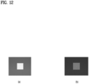
- FIG. 12 illustrates an example of a grayscale representation in a state in which a black film is formed on a front surface of a display device as a comparative example
- FIG. 13 illustrates an example of a grayscale representation of a display device using a light emitting device according to an embodiment of the present disclosure.
- FIG. 12 a black film is applied to a front surface including a top side of the light emitting device 200.
- FIG. 12 (a) shows a state before the black film is applied
- FIG. 12 (b) shows a state after the black film is applied.
- a central white region is bright, but a periphery before application of the black film is not sufficiently dark. This may be a phenomenon in which a sapphire mainly used as the support layer 240 of the light emitting device 200 has a large reflectivity with respect to external incident light.
- the contrast o of the display may be lowered, and it may be difficult to achieve sufficient grayscale representation.
- the black layer 310 is not positioned on the light emitting device 200, it may be seen that a central portion may be sufficiently bright, and a periphery may be sufficiently dark owing to an operation of the black layer 310.
- a light source (e.g., light emitting device 200) side may be represented to be sufficiently bright, and a periphery of the light source may be represented to be sufficiently dark. Accordingly, a grayscale representation by the light source may be widely implemented.
- the black layer 310 is not disposed on the light emitting device 200, the overall brightness of the display device may be improved.
- light traveling to the side surface of the light emitting device 200 may proceed to a front surface, thereby increasing light efficiency.
- viewing angles due to different light distribution characteristics among red, green, and blue may be uniformized.
- a display device using a Light Emitting Diode may be provided.
- LED Light Emitting Diode
Landscapes
- Electroluminescent Light Sources (AREA)
- Devices For Indicating Variable Information By Combining Individual Elements (AREA)
Abstract
Description
- The present disclosure is applicable to a technical field related to a display device and relates to a display device using a Light Emitting Diode (LED) and a method of fabricating the same.
- As the information society develops, demand for a display device increases in various forms, and in response thereto, various display devices such as a Liquid Crystal Display (LCD) device, a Plasma Display Panel (PDP), an Electro Luminescent Display (ELD), a Vacuum Fluorescent Display (VFD), an Organic Light Emitting Diode (OLED), a Micro Light Emitting Diode (Micro LED), and the like are being studied and used.
- A digital signage is a display device that provides specific information as well as a broadcasting program in public places such as airport, hotel, hospital, and subway station, and the like, as a communication tool capable of inducing marketing, advertisement, training effects, and customer experience of enterprises as well as a general TV.
- A digital signage is a medium for displaying various contents and commercial advertisements by installing a display panel such as a Liquid Crystal Display (LCD), a Plasma Display Panel (PDP), an Organic Light Emitting Diode (OLED), a Micro LED Light Emitting Diode (LED), etc. in certain outdoor places or devices such as street furniture, and may be installed on public movement lines such as apartment elevators, subway stations, subway trains, buses, universities, banks, convenience stores, discount stores, and shopping malls, and the like.
- Recently, many studies have been conducted to improve an image quality of a display panel while the digital signage is large- or ultra-large sized.
- Such digital signage is implemented as a modular display device in which various display modules are configured to be combined. Such a module display may use a Light Emitting Diode (LED) as a pixel.
- When a light emitting device is used as a pixel (light source), when a black film is not applied to an upper side of the light emitting device, a central pixel area may be brightly represented but a periphery of the light source may not be represented sufficiently dark. This may be a phenomenon in which a sapphire used in the light emitting device has a large reflectivity with respect to an external incident light.
- In addition, when the black film is applied, the periphery of the light source may be represented to be sufficiently dark but the central white area may be darkened together by the application of the black film.
- Accordingly, contrast of a display may be reduced and a sufficient grayscale representation may be difficult.
- Therefore, a demand for a solution for such problems has emerged.
- One technical task of the present disclosure is to provide a display device using a light emitting device and fabricating method thereof, by which light efficiency may be improved.
- Another technical task of the present disclosure is to provide a display device using a light emitting device and fabricating method thereof, by which a grayscale representation by a light source may be widely implemented.
- Another technical task of the present disclosure is to provide a stacked light emitting device and display device using the same, which may increase light efficiency by allowing light traveling to a side surface of a light emitting device to travel on a front surface,.
- Another technical task of the present disclosure is to provide a stacked light emitting device and display device using the same, which may uniformize a viewing angle due to different light distribution characteristics among red, green, and blue.
- Another technical task of the present disclosure is to provide a stacked light emitting device and display device using the same, which may improve a phenomenon in which a bright line occurs between modules when the display device has module structures connected to each other.
- Furthermore, the technical tasks to be achieved in the embodiments are not limited to the above-mentioned matters, and other unmentioned technical tasks may be considered by those skilled in the art from various embodiments to be described below.
- In a first technical aspect of the present disclosure, provided is a display device including a wiring substrate, a light emitting device disposed as an individual pixel on the wiring substrate, an insulating layer positioned on at least a side surface of the light emitting device, and a black layer positioned on the insulating layer, wherein the black layer may include a material formed by transforming a material forming the insulating layer.
- The black layer may include a material formed by carbonizing particles included in the insulating layer.
- The black layer may include a material formed by decomposing particles included in the insulating layer by heat.
- The material decomposed by the heat may include non-crystalline carbon and amorphous powder.
- The black layer may have a predetermined thickness on the insulating layer.
- The insulating layer may act as a reflective layer.
- The insulating layer may include a transparent resin layer and particles dispersed in the transparent resin layer.
- The transparent resin layer may include at least one of silicon, epoxy, or urethane.
- The particle may include at least one of silicon oxide, titanium oxide, or zirconium oxide.
- A refractive index of the particle may be different from that of the transparent resin layer.
- The light emitting device may include a semiconductor structure having a plurality of semiconductor layers stacked to emit light of a first color, a second color, and a third color.
- The light emitting device may include a support layer on the semiconductor structure.
- The insulating layer may be positioned to further surround a side surface of the support layer.
- The black layer may be positioned to surround at least a portion of a side surface of the support layer.
- In a second technical aspect of the present disclosure, provided is a method of fabricating a display device using a light emitting device, the method including disposing a plurality of light emitting devices forming individual pixels on a wiring substrate, forming an insulating layer including particles dispersed in a transparent resin layer between the light emitting devices, and forming a black layer by applying heat to the insulating layer.
- The applying the heat to the insulating layer may be performed by laser irradiation.
- The forming the black layer may include thermally decomposing particles included in the insulating layer by applying the heat.
- A lens may be positioned on the light emitting device so as not to react to the laser irradiation.
- First, according to an embodiment of the present disclosure, a light source (light emitting device) side may be represented bright sufficiently, and a periphery of the light source may be represented sufficiently dark. Accordingly, a grayscale representation by the light source may be widely implemented.
- In addition, since a black layer is not positioned on a light emitting device, an overall brightness of a display device may be improved.
- In addition, the light traveling to a side surface of a light emitting device is allowed to travel to a front surface, thereby increasing light efficiency.
- In addition, viewing angles due to different light distribution characteristics among red, green, and blue may be uniformized.
- In addition, when a display device has a module structure connected to each other, a phenomenon in which a bright line occurs between modules may be improved.
- In addition, a size of a light emitting device may be substantially expanded.
- The effects obtained from the embodiments are not limited to the effects mentioned above, and other unmentioned effects may be clearly derived and understood by those skilled in the art based on the following detailed description.
-
-
FIG. 1 is a cross-sectional diagram illustrating pixel regions of a display device using a light emitting device according to an embodiment of the present disclosure. -
FIG. 2 is a cross-sectional diagram illustrating a unit pixel region of a display device using a light emitting device according to an embodiment of the present disclosure. -
FIG. 3 is an enlarged diagram illustrating a display device using a light emitting device according to an embodiment of the present disclosure. -
FIG. 4 is a cross-sectional diagram illustrating a light emitting device of a display device using the light emitting device according to an embodiment of the present disclosure. -
FIG. 5 is a cross-sectional diagram illustrating a modified example of the light emitting device ofFIG. 4 . -
FIG. 6 is a cross-sectional diagram illustrating a light emitting device of a display device using the light emitting device according to another embodiment of the present disclosure. -
FIG. 7 is a cross-sectional diagram illustrating a modified example of the light emitting device ofFIG. 6 . -
FIG. 8 is a cross-sectional diagram illustrating a display device using a light emitting device according to another embodiment of the present disclosure. -
FIG. 9 is a schematic cross-sectional diagram illustrating a process of fabricating a display device using a light emitting device according to an embodiment of the present disclosure. -
FIG. 10 is a schematic diagram illustrating a partial region ofFIG. 9 . -
FIG. 11 is a flowchart illustrating a process of fabricating a display device using a light emitting device according to an embodiment of the present disclosure. -
FIG. 12 is a diagram illustrating an example of a grayscale representation in a state in which a black film is formed on a front surface of a display device as a comparative example. -
FIG. 13 is a diagram illustrating an example of a grayscale representation of a display device using a light emitting device according to an embodiment of the present disclosure. - Reference will now be made in detail to embodiments of the present disclosure, examples of which are illustrated in the accompanying drawings. Wherever possible, the same reference numbers will be used throughout the drawings to refer to the same or like parts, and redundant description thereof will be omitted. As used herein, the suffixes "module" and "unit" are added or used interchangeably to facilitate preparation of this specification and are not intended to suggest distinct meanings or functions. In describing embodiments disclosed in this specification, relevant well-known technologies may not be described in detail in order not to obscure the subject matter of the embodiments disclosed in this specification. In addition, it should be noted that the accompanying drawings are only for easy understanding of the embodiments disclosed in the present specification, and should not be construed as limiting the technical spirit disclosed in the present specification.
- Furthermore, although the drawings are separately described for simplicity, embodiments implemented by combining at least two or more drawings are also within the scope of the present disclosure.
- In addition, when an element such as a layer, region or module is described as being "on" another element, it is to be understood that the element may be directly on the other element or there may be an intermediate element between them.
- A display device described in the present specification is a concept including all display devices displaying information as a unit pixel or a set of unit pixels. Therefore, the present disclosure is not limited to a finished product and may be applicable to a component. For example, a panel corresponding to one component of a digital TV may also independently correspond to a display device of the present specification. The finished product may include a mobile phone, a smart phone, a laptop computer, a digital broadcasting terminal, Personal Digital Assistants (PDA), a Portable Multimedia Player (PMP), a navigation, a slate PC, a tablet PC, an Ultra Book, a digital TV, a desktop computer, etc.
- However, it will be readily apparent to those skilled in the art that the configuration according to embodiments described herein may be applied to a device capable of displaying even in the form of a new product to be developed later.
- In addition, the semiconductor light emitting device mentioned in this specification is a concept including an LED, a micro LED, and the like, which may be used in a mixed manner.
-
FIG. 1 is a cross-sectional diagram illustrating pixel regions of a display device using a light emitting device according to an embodiment of the present disclosure.FIG. 2 is a cross-sectional diagram illustrating a unit pixel region of a display device using a light emitting device according to an embodiment of the present disclosure.FIG. 3 is an enlarged diagram illustrating a display device using a light emitting device according to an embodiment of the present disclosure. - Referring to
FIG. 1 , in adisplay device 10, light emittingdevices 200 that form a plurality of pixels may be arranged on awiring substrate 100 including abase substrate 120 provided with awiring electrode 110. - In this case, an insulating
layer 300 may be disposed between a plurality of thelight emitting devices 200. The insulatinglayer 300 may be disposed on at least a side surface of thelight emitting device 200 to surround the side surface of thelight emitting device 200. - In addition, as shown in
FIG. 1 , the insulatinglayer 300 may be provided to fill a space between the light emittingdevices 200. - A
black layer 310 may be disposed on the insulatinglayer 300. Theblack layer 310 may serve as a black matrix layer that improves contrast of thedisplay device 10. - The
black layer 310 may include a material formed by transforming a material forming the insulatinglayer 300. In an exemplary embodiment, theblack layer 310 may include a material formed by carbonizing particles included in the insulatinglayer 300. - In other words, the
black layer 310 may include a material in which particles included in the insulatinglayer 300 are decomposed by heat. In this case, the material decomposed by the heat may include non-crystalline carbon. - The
black layer 310 may be formed by carbonization of a resin included in the insulatinglayer 300. This carbonization phenomenon may be a phenomenon in which an organic material is pyrolyzed under appropriate conditions to generate non-crystalline carbon-black amorphous micropowder (soot). This will be described in detail later. - As shown in
FIG. 1 , in an exemplary embodiment, theblack layer 310 may have a predetermined thickness on the insulatinglayer 300. However, depending on embodiments, the thickness of theblack layer 310 may vary depending on a distance between the light emittingdevices 200. - The insulating
layer 300 may serve as a reflective layer. That is, the insulatinglayer 300 may serve as a reflective layer that reflects light emitted from thelight emitting device 200 to the side surface. Meanwhile, the insulatinglayer 300 may insulate afirst electrode 250 and asecond electrode 260 of thelight emitting device 200. In addition, the insulatinglayer 300 may act as a layer that fills a space between the light emittingdevices 200 to planarize. Hereinafter, the insulatinglayer 300 and thereflective layer 300 may be interchangeably described, and will be described using the same reference number. - Referring to
FIG. 3 , the insulatinglayer 300 may includeparticles 303 dispersed in atransparent resin layer 302. Theparticles 303 may act as reflective particles. This will be described in detail later. - In
FIG. 1 , thewiring electrode 110 is briefly illustrated. A plurality ofwiring electrodes 110 may be divided and positioned on thewiring substrate 110. Here, thewiring electrode 110 may include a data electrode (pixel electrode) and a scan electrode (common electrode). - Although not shown, the
wiring electrode 110 arranged on thewiring substrate 100 may be connected to a TFT layer provided with a Thin Film Transistor (TFT). The data electrode (pixel electrode) may be connected to the TFT layer. A detailed description thereof will be omitted. - In an exemplary embodiment, as illustrated, the insulating
layer 300 may have ahang structure 301 between the light emittingdevices 200 neighboring to each other. That is, acurved structure 301 which is concavely formed between the neighboring light emittingdevices 200 and continuously extends may be formed on a top surface of the insulatinglayer 300. - In other words, a maximum height of the
light emitting device 200 and a minimum height of the insulatinglayer 300 may be different from each other. For example, the minimum height of the insulatinglayer 300 may be lower than the maximum height of thelight emitting device 200. In other words, the height of thehang structure 301 may be higher than half of the height of thelight emitting device 200. - The
hang structure 301 may be associated with a fabricating process of the insulatinglayer 300. For example, when the insulatinglayer 300 is formed using a jetting process of coating a material using a nozzle and then curing the material, thehang structure 301 may be formed. - The
light emitting device 200 may be disposed on thewiring substrate 100 while forming an individual pixel. For example, a singlelight emitting device 200 may be configured to form a single pixel. Since the insulatinglayer 300 surrounding at least a side surface of the singlelight emitting device 200 constituting the individual pixel and acting as a reflective layer is formed, light emitted from thelight emitting device 200 may be emitted upward without being mixed with light emitted from anotherlight emitting device 200 constituting a neighboring pixel. - That is, since light is emitted in all directions from the
light emitting device 200, the light emitted laterally from the individuallight emitting devices 200 may be reflected by the insulatinglayer 300 and emitted toward an upper side of thedisplay device 10. - Accordingly, since light emitted from the
light emitting device 200 and traveling to the side surface is blocked by the insulatinglayer 300, it is possible to fundamentally prevent a phenomenon in which a bright line is generated between the pixels in thedisplay device 10. - Referring to
FIG. 2 , for example, thelight emitting device 200 constituting the individual pixel may include asemiconductor structure 202 including a plurality ofsemiconductor layers - As a specific example, the
light emitting device 200 may be a stacked semiconductor light emitting device capable of emitting red, green, and blue light. - For example, the stacked
light emitting device 200 may include asemiconductor structure 202 including afirst semiconductor layer 210 emitting red light, asecond semiconductor layer 220 emitting blue light, and athird semiconductor layer 230 emitting green light. - Here, the
first semiconductor layer 210, thesecond semiconductor layer 220, and thethird semiconductor layer 230 may include semiconductor layers capable of emitting lights of individual colors, respectively. For example, each of thefirst semiconductor layer 210, thesecond semiconductor layer 220, and thethird semiconductor layer 230 may include an active layer capable of emitting light of an individual color. As another example, each of thefirst semiconductor layer 210, thesecond semiconductor layer 220, and thethird semiconductor layer 230 may include a n-type semiconductor layer and a p-type semiconductor layer together with an active layer capable of emitting light of an individual color. Such an individual structure is omitted fromFIG. 2 . - In addition, the
light emitting device 200 may include afirst electrode 250 and asecond electrode 260 electrically connected to one side and the other side of the semiconductor structure, respectively. InFIG. 2 , an electrical connection structure of the semiconductor structure, thefirst electrode 250, and thesecond electrode 260 is briefly illustrated. - A
support layer 240 may be disposed on thesemiconductor structure 202. Here, thesupport layer 240 may be a growth substrate in which thesemiconductor structure 202 is grown or a transfer substrate in which thesemiconductor structure 202 is transferred and bonded. Thesupport layer 240 may be transparent to light emitted from thesemiconductor structure 202. For example, thesupport layer 240 may include a sapphire substrate. - According to an embodiment, a lens 350 (see
FIG. 10 ) may be disposed on thesupport layer 240. Thelens 350 does not react in the process of forming theblack layer 310 so that thelight emitting device 200 is allowed not to react with heat. - Meanwhile, the
first electrode 250 and thesecond electrode 260, which are electrically connected to one side and the other side of thesemiconductor structure 202, respectively, may be provided withextension pads extension pads semiconductor structure 202. - The
light emitting device 200 as a light source will be described later in detail. - Here, the insulating
layer 300 acts as a reflective layer and may be positioned to surround at least the side surface of thesemiconductor structure 202 including thefirst semiconductor layer 210, thesecond semiconductor layer 220, and thethird semiconductor layer 230 of thelight emitting device 200. - In addition, the insulating
layer 300 may be positioned to cover thefirst electrode 250 and thesecond electrode 260. In addition, for example, the insulatinglayer 300 may be positioned to cover theextension pads - The insulating
layer 300 may be positioned to further surround a side surface of thesupport layer 240 of thelight emitting device 200. For example, the insulatinglayer 300 may be positioned to surround all surfaces except for a top surface of thesupport layer 240 of the light emitting device. - As described above, the
black layer 310 may have a predetermined thickness on the insulatinglayer 300. That is, a thickness 'a' of theblack layer 310 at a portion close to thelight emitting device 200 may be the same as a thickness 'a" of a portion of theblack layer 310 relatively far from thelight emitting device 200. - This may mean that the predetermined thickness is formed along the insulating
layer 300 by the above-mentioned carbonization (or pyrolysis) process. In addition, it may mean that theblack layer 310 may be formed in a manner that a heat source for carbonization (or pyrolysis) penetrates into the insulating layer to a predetermined depth irrespective of a position. - Referring to
FIG. 3 , the insulatinglayer 300 may includeparticles 303 dispersed in thetransparent resin layer 302. Theseparticles 303 may act as reflective particles. - In an exemplary embodiment, a refractive index of the
particle 303 may be different from that of thetransparent resin layer 302. - The
particle 303 may include at least one of silicon, titanium, zirconium, or an oxide thereof, e.g., silicon oxide (SiOx), titanium oxide (TiOx), or zirconium oxide (ZrOx). - Meanwhile, the
transparent resin layer 302 may be formed of a resin material. For example, thetransparent resin layer 302 may include at least one of silicon, epoxy, and urethane. - A thickness of the insulating
layer 300 may be set to have a reflectivity of 90% or more by thetransparent resin layer 302 and theparticles 303. -
FIG. 4 is a cross-sectional diagram illustrating a light emitting device of a display device using the light emitting device according to an embodiment of the present disclosure.FIG. 5 is a cross-sectional diagram illustrating a modified example of the light emitting device ofFIG. 4 . - Referring to
FIG. 4 , alight emitting device 201 constituting an individual pixel may include asemiconductor structure 202 including a plurality ofsemiconductor layers - As a specific example, the
light emitting device 201 may be a stacked semiconductor light emitting device capable of emitting red, green, and blue light. - For example, the stacked
light emitting device 201 may include asemiconductor structure 202 including afirst semiconductor layer 210 emitting red light, asecond semiconductor layer 220 emitting blue light, and athird semiconductor layer 230 emitting green light. - Here, the
first semiconductor layer 210, thesecond semiconductor layer 220, and thethird semiconductor layer 230 may include semiconductor layers capable of emitting light of individual colors, respectively. For example, each of thefirst semiconductor layer 210, thesecond semiconductor layer 220, and thethird semiconductor layer 230 may include an active layer capable of emitting light of an individual color. As another example, each of thefirst semiconductor layer 210, thesecond semiconductor layer 220, and thethird semiconductor layer 230 may include a n-type semiconductor layer and a p-type semiconductor layer together with an active layer capable of emitting light of an individual color. - In addition, the
light emitting device 201 may include afirst electrode 250 and asecond electrode 260 electrically connected to one side and the other side of thesemiconductor structure 202, respectively. - A
support layer 240 may be disposed on thesemiconductor structure 202. Here, thesupport layer 240 may be a growth substrate in which thesemiconductor structure 202 is grown or a transfer substrate in which thesemiconductor structure 202 is transferred and bonded. A surface direction size of thesupport layer 240 may be greater than thesemiconductor structure 202. - A
reflective layer semiconductor structure 202 of thelight emitting device 201. - Here, the
reflective layer semiconductor structure 202 including at least thefirst semiconductor layer 210, thesecond semiconductor layer 220, and thethird semiconductor layer 230 of thelight emitting device 200. - In addition, the
reflective layer first electrode 250 and thesecond electrode 260. - The
reflective layer support layer 240 of thelight emitting device 201. For example, the insulatinglayer 270 may be positioned to surround all surfaces except for a top surface of thesupport layer 240 of the light emitting device. - In this case, as an exemplary embodiment, the reflective layer may include a first
reflective layer 271 covering side and bottom surfaces of the semiconductor structure including thefirst semiconductor layer 210, thesecond semiconductor layer 220, and thethird semiconductor layer 230 and a secondreflective layer 270 covering side surfaces of the firstreflective layer 271 and thesupport layer 240. - The
reflective layer light emitting device 201. A light emitting surface of thelight emitting device 201 may be expanded to a size including thereflective layer reflective layers - Referring to
FIG. 5 ,extension pads first electrode 250 and thesecond electrode 260 may be further provided. - A size of the
extension pad 251/261 may become greater over an outer surface of thesemiconductor structure 202. For example, the size of theextension pad 251/261 may be extended to an outer surface of thereflective layer 270. - In this case, top surfaces of the
extension pads reflective layer extension pad 251/261 may further improve the reflectivity of thereflective layer 270/271. In addition, theextension pad 251/261 may form a substantially external electrode pad of thelight emitting device 201. - For other matters not described, the matters described above with reference to
FIGs. 1 to 3 may be applied as they are. For example, as described with reference toFIG. 3 , thereflective layer particles 303 dispersed in thetransparent resin layer 302. That is, the characteristics of thereflective layer reflective layer 300 described above. In other words, the characteristics of thereflective layer hang structure 301 may be the same as those of thereflective layer 300 described above. Therefore, redundant descriptions will be omitted. -
FIG. 6 is a cross-sectional diagram illustrating a light emitting device of a display device using the light emitting device according to another embodiment of the present disclosure.FIG. 7 is a cross-sectional diagram illustrating a modified example of the light emitting device ofFIG. 6 . - Referring to
FIG. 6 , alight emitting device 201 constituting an individual pixel may include asemiconductor structure 202 including a plurality ofsemiconductor layers semiconductor structure 202 is the same as that described with reference toFIG. 4 , a redundant description thereof will be omitted. - In addition, the
light emitting device 201 may include afirst electrode 250 and asecond electrode 260 electrically connected to one side and the other side of thesemiconductor structure 202, respectively. - A
support layer 240 may be disposed on thesemiconductor structure 202. Here, thesupport layer 240 may be a growth substrate in which thesemiconductor structure 202 is grown or a transfer substrate in which thesemiconductor structure 202 is transferred and bonded. A surface direction size of thesupport layer 240 may be greater than thesemiconductor structure 202. - A
reflective layer semiconductor structure 202 of thelight emitting device 201. - In an exemplary embodiment, the reflective layer may include a first
reflective layer 271 covering a side surface of thesemiconductor structure 202 including thefirst semiconductor layer 210, thesecond semiconductor layer 220, and thethird semiconductor layer 230 and side surfaces of thefirst electrode 250 and thesecond electrode 260 and a secondreflective layer 272 covering side and top surfaces of the firstreflective layer 271 and thesupport layer 240. - As described above, the second
reflective layer 272 may be positioned to surround the side and top surfaces of thesupport layer 240 of thelight emitting device 201. The secondreflective layer 272 may improve uniformity of light emitted from thelight emitting device 201. - The
reflective layer light emitting device 201. A light emitting surface of thelight emitting device 201 may be expanded to a size including thereflective layer semiconductor structure 202 may be expanded to a size including thereflective layer - Referring to
FIG. 7 ,extension pads first electrode 250 and thesecond electrode 260 may be further provided. - A size of the
extension pads semiconductor structure 202. For example, the size of theextension pads reflective layer 272. - In this case, top surfaces of the
extension pads reflective layer extension pads reflective layer extension pad 251/261 may form a substantially external electrode pad of thelight emitting device 201. - For other matters not described, the matters described with reference to
FIGS. 1 to 5 above may be applied as they are. For example, as described with reference toFIG. 3 , thereflective layer 271/272 may includeparticles 303 dispersed in thetransparent resin layer 302. That is, the characteristics of thereflective layer 271/272 of the present embodiment may be substantially the same as those of thereflective layer 300 described above. In other words, the characteristics of thereflective layer 271/272 of the present embodiment except for the characteristics having thehang structure 301 may be the same as those of thereflective layer 300 described above. Therefore, redundant descriptions will be omitted. -
FIG. 8 is a cross-sectional diagram illustrating a display device using a light emitting device according to another embodiment of the present disclosure. - Referring to
FIG. 8 , an embodiment of thedisplay device 10 in which thelight emitting device 201 according to the embodiment ofFIG. 4 forms an individual pixel is illustrated. - That is, the
light emitting device 201 according to the embodiment ofFIG. 5 may be installed on awiring substrate 100 to form an individual pixel. In this case, agap layer 400 may filled a space between the individuallight emitting devices 201. - As described above, the
display device 10 may be implemented in a simple structure by using thelight emitting device 201 having the structure expanded by areflective layer - In this case, a
module display device 10 having a predetermined number of light emittingdevices 201 may be implemented on thewiring substrate 100 having a predetermined size. Thedisplay device 10 having a desired size may be fabricated by combining themodule display device 10. -
FIG. 9 is a schematic cross-sectional diagram illustrating a process of fabricating a display device using a light emitting device according to an embodiment of the present disclosure.FIG. 10 is a schematic diagram illustrating a partial region ofFIG. 9 .FIG. 11 is a flowchart illustrating a process of fabricating a display device using a light emitting device according to an embodiment of the present disclosure. - Referring to
FIG. 9 , a process of forming ablack layer 310 is schematically illustrated. - Referring to
FIG. 11 together, in a process for fabricating a display device using a light emitting device according to an embodiment of the present disclosure, first, a step S10 of disposing a plurality of light emittingdevices 200 forming individual pixels on awiring substrate 100 may be performed. - Thereafter, a step S20 of forming an insulating
layer 300 includingparticles 303 dispersed in atransparent resin layer 302 between the light emittingdevices 200 may be performed. - Next, a step S30 of forming a
black layer 310 by applying heat to the insulatinglayer 300 may be performed. -
FIG. 9 andFIG. 10 mainly illustrate the step S30 of forming theblack layer 310 by applying heat to the insulatinglayer 300. - In an exemplary embodiment, the step of applying heat to the insulating
layer 300, that is, the step S30 of forming theblack layer 310 may be performed by laser irradiation. Theblack layer 310 may be formed by thermally decomposing theparticles 303 included in the insulatinglayer 300 in a manner of applying heat to the insulatinglayer 300 by the laser irradiation. The resin (resin) may be carbonized by a pyrolysis process of theparticles 303 or thetransparent resin layer 302. - Such a carbonization phenomenon may be a phenomenon in which an organic material is pyrolyzed under appropriate conditions to generate non-crystalline carbon-black amorphous micropowder (soot).
- That is, at least one of the
transparent resin layer 302 and theparticles 303 may be thermally decomposed by heat generated by irradiating a laser to the insulatinglayer 300, and in this process, non-crystalline carbon, for example, black amorphous micropowder may be generated. - As described above, the
transparent resin layer 302 may be formed of a resin material. For example, thetransparent resin layer 302 may include at least one of silicon, epoxy, and urethane. The material forming thetransparent resin layer 302 may be changed in shape by laser light. That is, the resin material forming thetransparent resin layer 302 may be carbonized by laser light to form theblack layer 310. - The step S30 of forming the
black layer 310 may be performed by irradiating laser light to all over thedisplay 10. In this process, the laser light may react only to the insulatinglayer 300. That is, thelight emitting device 200 may not react with the laser light. The laser light may penetrate the insulatinglayer 300 at a predetermined depth according to a set wavelength and power to apply heat thereto. - In the process of applying heat to the insulating
layer 300, thelight emitting devices 200 are disposed on thewiring substrate 100, and in a state in which the insulatinglayer 300 is formed between the light emittingdevices 200, the laser light may be irradiated while moving along theentire wiring substrate 100. Alternatively, laser light may be irradiated while thewiring substrate 100 moves in a state in which the laser is fixed. - Referring to
FIG. 10 , alens 350 that does not react to a laser irradiation may be disposed on thelight emitting device 200. - Laser light may not react to the
support layer 240 disposed on a top side of thelight emitting device 200. Thesupport layer 240 may be formed of a material such as sapphire, and the laser light may pass through the sapphire, but the power of the laser light may not damage thesemiconductor structure 202. - However, the
lens 350 may be positioned on thesupport layer 240 so that the laser light may not pass through thesupport layer 240 or the power for the laser light to pass through thesupport layer 240 may be adjusted to greatly decrease. - As described above, in
FIG. 10 , the laser light may form a reactive region R only on the insulatinglayer 300 and a non-reactive region N on thelight emitting device 200. - Therefore, when the laser light passes from a left side to a right side in
FIG. 10 , the laser light may react to the insulatinglayer 300 only in the reaction region R located at the left and right sides of thelight emitting device 200 to form theblack layer 310. - Accordingly, the
black layer 310 may include a material formed by transforming a material forming the insulatinglayer 300. In an exemplary embodiment, theblack layer 310 may include a material formed by carbonizing particles included in the insulatinglayer 300. - In other words, the
black layer 310 may include a material in which particles included in the insulatinglayer 300 are decomposed by heat. In this case, the material decomposed by the heat may include non-crystalline carbon or amorphous powder. -
FIG. 12 illustrates an example of a grayscale representation in a state in which a black film is formed on a front surface of a display device as a comparative example, andFIG. 13 illustrates an example of a grayscale representation of a display device using a light emitting device according to an embodiment of the present disclosure. - Referring to
FIG. 12 , a black film is applied to a front surface including a top side of thelight emitting device 200.FIG. 12 (a) shows a state before the black film is applied, andFIG. 12 (b) shows a state after the black film is applied. - Referring to
FIG. 12 (a) , it may be seen that a central white region is bright, but a periphery before application of the black film is not sufficiently dark. This may be a phenomenon in which a sapphire mainly used as thesupport layer 240 of thelight emitting device 200 has a large reflectivity with respect to external incident light. - In addition, referring to
FIG. 12 (b) , it may be seen that a periphery is sufficiently dark but a central white region is darkened together by the application of the black film. - Therefore, according to the comparative example shown in
FIG. 12 , the contrast o of the display may be lowered, and it may be difficult to achieve sufficient grayscale representation. - Meanwhile, referring to
FIG. 13 according to an embodiment of the present disclosure, since theblack layer 310 is not positioned on thelight emitting device 200, it may be seen that a central portion may be sufficiently bright, and a periphery may be sufficiently dark owing to an operation of theblack layer 310. - That is, a light source (e.g., light emitting device 200) side may be represented to be sufficiently bright, and a periphery of the light source may be represented to be sufficiently dark. Accordingly, a grayscale representation by the light source may be widely implemented.
- In addition, since the
black layer 310 is not disposed on thelight emitting device 200, the overall brightness of the display device may be improved. - In addition, light traveling to the side surface of the
light emitting device 200 may proceed to a front surface, thereby increasing light efficiency. - In addition, viewing angles due to different light distribution characteristics among red, green, and blue may be uniformized.
- The above description is merely illustrative of the technical idea of the present disclosure. Those of ordinary skill in the art to which the present disclosure pertains will be able to make various modifications and variations without departing from the essential characteristics of the present disclosure.
- Therefore, embodiments disclosed in the present disclosure are not intended to limit the technical idea of the present disclosure, but to describe, and the scope of the technical idea of the present disclosure is not limited by such embodiments.
- The scope of protection of the present disclosure should be interpreted by the claims below, and all technical ideas within the scope equivalent thereto should be construed as being included in the scope of the present disclosure.
- According to the present disclosure, a display device using a Light Emitting Diode (LED) may be provided.
Claims (20)
- A display device, comprising:a wiring substrate;a light emitting device disposed as an individual pixel on the wiring substrate;an insulating layer positioned on at least a side surface of the light emitting device; anda black layer positioned on the insulating layer,wherein the black layer includes a material formed by the transformation of a material constituting the insulating layer.
- The display device of claim 1, wherein the black layer comprises a material formed by the carbonization of particles included in the insulating layer.
- The display device of claim 1, wherein the black layer includes a material formed by the decomposition of particles included in the insulating layer due to heat.
- The display device of claim 3, wherein the material formed by the decomposition of particles due to the heat comprises non-crystalline carbon and amorphous powder.
- The display device of claim 1, wherein the black layer has a predetermined thickness on the insulating layer.
- The display device of claim 1, wherein the insulating layer acts as a reflective layer.
- The display device of claim 1, the insulating layer comprising:a transparent resin layer; andparticles dispersed within the transparent resin layer.
- The display device of claim 7, wherein the transparent resin layer comprises at least one of silicon, epoxy, or urethane.
- The display device of claim 7, wherein the particle comprises at least one of silicon oxide, titanium oxide, or zirconium oxide.
- The display device of claim 7, wherein a refractive index of the particle is different from that of the transparent resin layer.
- The display device of claim 1, wherein the light emitting device comprises a semiconductor structure having a plurality of semiconductor layers stacked to emit light of a first color, a second color, and a third color.
- The display device of claim 11, wherein the light emitting device comprises a support layer on the semiconductor structure.
- The display device of claim 12, wherein the insulating layer is positioned to further surround a side surface of the support layer.
- The display device of claim 12, wherein the black layer is positioned to surround at least a portion of a side surface of the support layer.
- A method of fabricating a display device using a light emitting device, the method comprising:disposing a plurality of light emitting devices forming individual pixels on a wiring substrate;forming an insulating layer including particles dispersed within a transparent resin layer between the light emitting devices; andforming a black layer by applying heat to the insulating layer.
- The method of claim 15, wherein the forming the black layer is performed by laser irradiation.
- The method of claim 16, wherein the forming the black layer comprises thermally decomposing particles included in the insulating layer by applying the heat.
- The method of claim 17, wherein the terminally decomposed particles comprise non-crystalline carbon and amorphous powder.
- The method of claim 15, wherein a lens is positioned on the light emitting device so as not to react to the laser irradiation.
- The method of claim 15, the insulating layer comprising:a transparent resin layer; andparticles dispersed within the transparent resin layer.
Applications Claiming Priority (2)
| Application Number | Priority Date | Filing Date | Title |
|---|---|---|---|
| KR20220018228 | 2022-02-11 | ||
| PCT/KR2022/017887 WO2023153590A1 (en) | 2022-02-11 | 2022-11-14 | Display device using light-emitting element and manufacturing method thereof |
Publications (2)
| Publication Number | Publication Date |
|---|---|
| EP4471864A1 true EP4471864A1 (en) | 2024-12-04 |
| EP4471864A4 EP4471864A4 (en) | 2025-05-07 |
Family
ID=87564459
Family Applications (1)
| Application Number | Title | Priority Date | Filing Date |
|---|---|---|---|
| EP22926188.8A Pending EP4471864A4 (en) | 2022-02-11 | 2022-11-14 | DISPLAY DEVICE USING LIGHT-EMITTING ELEMENT AND MANUFACTURING METHOD THEREOF |
Country Status (3)
| Country | Link |
|---|---|
| US (1) | US20250143057A1 (en) |
| EP (1) | EP4471864A4 (en) |
| WO (1) | WO2023153590A1 (en) |
Family Cites Families (8)
| Publication number | Priority date | Publication date | Assignee | Title |
|---|---|---|---|---|
| KR20130028350A (en) * | 2011-09-09 | 2013-03-19 | 엘지디스플레이 주식회사 | A patterned retarder type 3d display device having black strips and manufacturing method therefor |
| KR102492032B1 (en) * | 2016-04-04 | 2023-01-27 | 삼성디스플레이 주식회사 | Display device and method for fabricating the same |
| US11296262B2 (en) * | 2017-12-21 | 2022-04-05 | Lumileds Llc | Monolithic segmented LED array architecture with reduced area phosphor emission surface |
| TWI775712B (en) * | 2019-05-24 | 2022-08-21 | 晶元光電股份有限公司 | Package and display module |
| KR102764434B1 (en) * | 2019-05-30 | 2025-02-10 | 삼성디스플레이 주식회사 | Display device and manufacturing method thereof |
| KR102694326B1 (en) * | 2019-10-11 | 2024-08-13 | 삼성전자주식회사 | Display module and manafacturing method thereof |
| DE102019220379A1 (en) * | 2019-12-20 | 2021-06-24 | OSRAM Opto Semiconductors Gesellschaft mit beschränkter Haftung | RADIATION-EMITTING SEMICONDUCTOR COMPONENT AND METHOD FOR MANUFACTURING A RADIATION-EMITTING SEMICONDUCTOR COMPONENT |
| JP7349393B2 (en) * | 2020-03-10 | 2023-09-22 | シャープ福山レーザー株式会社 | image display element |
-
2022
- 2022-11-14 WO PCT/KR2022/017887 patent/WO2023153590A1/en not_active Ceased
- 2022-11-14 EP EP22926188.8A patent/EP4471864A4/en active Pending
- 2022-11-14 US US18/835,513 patent/US20250143057A1/en active Pending
Also Published As
| Publication number | Publication date |
|---|---|
| WO2023153590A1 (en) | 2023-08-17 |
| EP4471864A4 (en) | 2025-05-07 |
| US20250143057A1 (en) | 2025-05-01 |
Similar Documents
| Publication | Publication Date | Title |
|---|---|---|
| US10847585B2 (en) | Organic light emitting display device including a sound generating apparatus | |
| US12100692B2 (en) | Display panel, preparation method thereof and display device | |
| KR100742633B1 (en) | Electrooptic device, method for producing the same, and electronic apparatus | |
| TWI587734B (en) | Organic EL device, method of manufacturing organic EL device, and electronic device | |
| US9356179B2 (en) | Display panel integrated with photoelectric device | |
| US8981391B2 (en) | Display panel with high transparency | |
| KR102330553B1 (en) | Display device using micro led and method for producing the same | |
| CN108269823A (en) | Light emitting display device and use its multiscreen display apparatus | |
| CN103943649A (en) | Oled display panel and driving method thereof | |
| US12087807B2 (en) | Display device, method of manufacturing the same, and tiled display device including the same | |
| US12148788B2 (en) | Display device and tiled display device including the same | |
| CN118382931A (en) | Display device including semiconductor light emitting element | |
| US20250294923A1 (en) | Backlight unit including a plurality of leds and associated distributed bragg reflectors | |
| EP4471864A1 (en) | Display device using light-emitting element and manufacturing method thereof | |
| CN111613652A (en) | Display panel | |
| CN106711255A (en) | Photoluminescent display panel | |
| KR20230084019A (en) | Layered type light emitting device and display device using same | |
| KR20230125595A (en) | Display module and display device | |
| EP4739042A1 (en) | Display device and manufacturing method therefor | |
| US20220415216A1 (en) | Display device and tiled display device including the same | |
| KR20240128622A (en) | Light emitting device package and display device using same | |
| KR102917219B1 (en) | Light emitting device package and display device using same | |
| US20250370295A1 (en) | Display apparatus | |
| US20250072182A1 (en) | Display device including a semiconductor light emitting device | |
| CN112614877B (en) | Array substrate, display panel and display device |
Legal Events
| Date | Code | Title | Description |
|---|---|---|---|
| STAA | Information on the status of an ep patent application or granted ep patent |
Free format text: STATUS: THE INTERNATIONAL PUBLICATION HAS BEEN MADE |
|
| PUAI | Public reference made under article 153(3) epc to a published international application that has entered the european phase |
Free format text: ORIGINAL CODE: 0009012 |
|
| STAA | Information on the status of an ep patent application or granted ep patent |
Free format text: STATUS: REQUEST FOR EXAMINATION WAS MADE |
|
| 17P | Request for examination filed |
Effective date: 20240828 |
|
| AK | Designated contracting states |
Kind code of ref document: A1 Designated state(s): AL AT BE BG CH CY CZ DE DK EE ES FI FR GB GR HR HU IE IS IT LI LT LU LV MC ME MK MT NL NO PL PT RO RS SE SI SK SM TR |
|
| REG | Reference to a national code |
Ref country code: DE Ref legal event code: R079 Free format text: PREVIOUS MAIN CLASS: H01L0027150000 Ipc: H10H0029010000 |
|
| A4 | Supplementary search report drawn up and despatched |
Effective date: 20250409 |
|
| RIC1 | Information provided on ipc code assigned before grant |
Ipc: H10H 29/855 20250101ALI20250403BHEP Ipc: H10H 29/01 20250101AFI20250403BHEP |
|
| DAV | Request for validation of the european patent (deleted) | ||
| DAX | Request for extension of the european patent (deleted) |