EP4467341A2 - Direkte generative synthese aus uv-induzierten solvatisierten elektronen in einem ausgangsstoff für halogeniertes material und nanopartikel mit negativer elektronenaffinität - Google Patents
Direkte generative synthese aus uv-induzierten solvatisierten elektronen in einem ausgangsstoff für halogeniertes material und nanopartikel mit negativer elektronenaffinität Download PDFInfo
- Publication number
- EP4467341A2 EP4467341A2 EP24206381.6A EP24206381A EP4467341A2 EP 4467341 A2 EP4467341 A2 EP 4467341A2 EP 24206381 A EP24206381 A EP 24206381A EP 4467341 A2 EP4467341 A2 EP 4467341A2
- Authority
- EP
- European Patent Office
- Prior art keywords
- ceramic
- carbon
- nanoparticle
- feedstock
- printer
- Prior art date
- Legal status (The legal status is an assumption and is not a legal conclusion. Google has not performed a legal analysis and makes no representation as to the accuracy of the status listed.)
- Granted
Links
Images



Classifications
-
- H—ELECTRICITY
- H10—SEMICONDUCTOR DEVICES; ELECTRIC SOLID-STATE DEVICES NOT OTHERWISE PROVIDED FOR
- H10P—GENERIC PROCESSES OR APPARATUS FOR THE MANUFACTURE OR TREATMENT OF DEVICES COVERED BY CLASS H10
- H10P14/00—Formation of materials, e.g. in the shape of layers or pillars
- H10P14/20—Formation of materials, e.g. in the shape of layers or pillars of semiconductor materials
- H10P14/26—Formation of materials, e.g. in the shape of layers or pillars of semiconductor materials using liquid deposition
- H10P14/265—Formation of materials, e.g. in the shape of layers or pillars of semiconductor materials using liquid deposition using solutions
-
- B—PERFORMING OPERATIONS; TRANSPORTING
- B23—MACHINE TOOLS; METAL-WORKING NOT OTHERWISE PROVIDED FOR
- B23K—SOLDERING OR UNSOLDERING; WELDING; CLADDING OR PLATING BY SOLDERING OR WELDING; CUTTING BY APPLYING HEAT LOCALLY, e.g. FLAME CUTTING; WORKING BY LASER BEAM
- B23K26/00—Working by laser beam, e.g. welding, cutting or boring
- B23K26/34—Laser welding for purposes other than joining
- B23K26/342—Build-up welding
-
- B—PERFORMING OPERATIONS; TRANSPORTING
- B28—WORKING CEMENT, CLAY, OR STONE
- B28B—SHAPING CLAY OR OTHER CERAMIC COMPOSITIONS; SHAPING SLAG; SHAPING MIXTURES CONTAINING CEMENTITIOUS MATERIAL, e.g. PLASTER
- B28B1/00—Producing shaped prefabricated articles from the material
- B28B1/001—Rapid manufacturing of 3D objects by additive depositing, agglomerating or laminating of material
-
- B—PERFORMING OPERATIONS; TRANSPORTING
- B32—LAYERED PRODUCTS
- B32B—LAYERED PRODUCTS, i.e. PRODUCTS BUILT-UP OF STRATA OF FLAT OR NON-FLAT, e.g. CELLULAR OR HONEYCOMB, FORM
- B32B18/00—Layered products essentially comprising ceramics, e.g. refractory products
-
- B—PERFORMING OPERATIONS; TRANSPORTING
- B33—ADDITIVE MANUFACTURING TECHNOLOGY
- B33Y—ADDITIVE MANUFACTURING, i.e. MANUFACTURING OF THREE-DIMENSIONAL [3D] OBJECTS BY ADDITIVE DEPOSITION, ADDITIVE AGGLOMERATION OR ADDITIVE LAYERING, e.g. BY 3D PRINTING, STEREOLITHOGRAPHY OR SELECTIVE LASER SINTERING
- B33Y10/00—Processes of additive manufacturing
-
- B—PERFORMING OPERATIONS; TRANSPORTING
- B33—ADDITIVE MANUFACTURING TECHNOLOGY
- B33Y—ADDITIVE MANUFACTURING, i.e. MANUFACTURING OF THREE-DIMENSIONAL [3D] OBJECTS BY ADDITIVE DEPOSITION, ADDITIVE AGGLOMERATION OR ADDITIVE LAYERING, e.g. BY 3D PRINTING, STEREOLITHOGRAPHY OR SELECTIVE LASER SINTERING
- B33Y30/00—Apparatus for additive manufacturing; Details thereof or accessories therefor
-
- B—PERFORMING OPERATIONS; TRANSPORTING
- B33—ADDITIVE MANUFACTURING TECHNOLOGY
- B33Y—ADDITIVE MANUFACTURING, i.e. MANUFACTURING OF THREE-DIMENSIONAL [3D] OBJECTS BY ADDITIVE DEPOSITION, ADDITIVE AGGLOMERATION OR ADDITIVE LAYERING, e.g. BY 3D PRINTING, STEREOLITHOGRAPHY OR SELECTIVE LASER SINTERING
- B33Y70/00—Materials specially adapted for additive manufacturing
-
- C—CHEMISTRY; METALLURGY
- C01—INORGANIC CHEMISTRY
- C01B—NON-METALLIC ELEMENTS; COMPOUNDS THEREOF; METALLOIDS OR COMPOUNDS THEREOF NOT COVERED BY SUBCLASS C01C
- C01B32/00—Carbon; Compounds thereof
- C01B32/05—Preparation or purification of carbon not covered by groups C01B32/15, C01B32/20, C01B32/25, C01B32/30
-
- C—CHEMISTRY; METALLURGY
- C01—INORGANIC CHEMISTRY
- C01B—NON-METALLIC ELEMENTS; COMPOUNDS THEREOF; METALLOIDS OR COMPOUNDS THEREOF NOT COVERED BY SUBCLASS C01C
- C01B32/00—Carbon; Compounds thereof
- C01B32/25—Diamond
- C01B32/26—Preparation
-
- C—CHEMISTRY; METALLURGY
- C01—INORGANIC CHEMISTRY
- C01B—NON-METALLIC ELEMENTS; COMPOUNDS THEREOF; METALLOIDS OR COMPOUNDS THEREOF NOT COVERED BY SUBCLASS C01C
- C01B32/00—Carbon; Compounds thereof
- C01B32/90—Carbides
- C01B32/914—Carbides of single elements
- C01B32/956—Silicon carbide
- C01B32/963—Preparation from compounds containing silicon
-
- C—CHEMISTRY; METALLURGY
- C04—CEMENTS; CONCRETE; ARTIFICIAL STONE; CERAMICS; REFRACTORIES
- C04B—LIME, MAGNESIA; SLAG; CEMENTS; COMPOSITIONS THEREOF, e.g. MORTARS, CONCRETE OR LIKE BUILDING MATERIALS; ARTIFICIAL STONE; CERAMICS; REFRACTORIES; TREATMENT OF NATURAL STONE
- C04B35/00—Shaped ceramic products characterised by their composition; Ceramics compositions; Processing powders of inorganic compounds preparatory to the manufacturing of ceramic products
- C04B35/515—Shaped ceramic products characterised by their composition; Ceramics compositions; Processing powders of inorganic compounds preparatory to the manufacturing of ceramic products based on non-oxide ceramics
- C04B35/52—Shaped ceramic products characterised by their composition; Ceramics compositions; Processing powders of inorganic compounds preparatory to the manufacturing of ceramic products based on non-oxide ceramics based on carbon, e.g. graphite
- C04B35/528—Shaped ceramic products characterised by their composition; Ceramics compositions; Processing powders of inorganic compounds preparatory to the manufacturing of ceramic products based on non-oxide ceramics based on carbon, e.g. graphite obtained from carbonaceous particles with or without other non-organic components
-
- C—CHEMISTRY; METALLURGY
- C04—CEMENTS; CONCRETE; ARTIFICIAL STONE; CERAMICS; REFRACTORIES
- C04B—LIME, MAGNESIA; SLAG; CEMENTS; COMPOSITIONS THEREOF, e.g. MORTARS, CONCRETE OR LIKE BUILDING MATERIALS; ARTIFICIAL STONE; CERAMICS; REFRACTORIES; TREATMENT OF NATURAL STONE
- C04B35/00—Shaped ceramic products characterised by their composition; Ceramics compositions; Processing powders of inorganic compounds preparatory to the manufacturing of ceramic products
- C04B35/515—Shaped ceramic products characterised by their composition; Ceramics compositions; Processing powders of inorganic compounds preparatory to the manufacturing of ceramic products based on non-oxide ceramics
- C04B35/56—Shaped ceramic products characterised by their composition; Ceramics compositions; Processing powders of inorganic compounds preparatory to the manufacturing of ceramic products based on non-oxide ceramics based on carbides or oxycarbides
- C04B35/5607—Shaped ceramic products characterised by their composition; Ceramics compositions; Processing powders of inorganic compounds preparatory to the manufacturing of ceramic products based on non-oxide ceramics based on carbides or oxycarbides based on refractory metal carbides
- C04B35/5611—Shaped ceramic products characterised by their composition; Ceramics compositions; Processing powders of inorganic compounds preparatory to the manufacturing of ceramic products based on non-oxide ceramics based on carbides or oxycarbides based on refractory metal carbides based on titanium carbides
-
- C—CHEMISTRY; METALLURGY
- C04—CEMENTS; CONCRETE; ARTIFICIAL STONE; CERAMICS; REFRACTORIES
- C04B—LIME, MAGNESIA; SLAG; CEMENTS; COMPOSITIONS THEREOF, e.g. MORTARS, CONCRETE OR LIKE BUILDING MATERIALS; ARTIFICIAL STONE; CERAMICS; REFRACTORIES; TREATMENT OF NATURAL STONE
- C04B35/00—Shaped ceramic products characterised by their composition; Ceramics compositions; Processing powders of inorganic compounds preparatory to the manufacturing of ceramic products
- C04B35/515—Shaped ceramic products characterised by their composition; Ceramics compositions; Processing powders of inorganic compounds preparatory to the manufacturing of ceramic products based on non-oxide ceramics
- C04B35/56—Shaped ceramic products characterised by their composition; Ceramics compositions; Processing powders of inorganic compounds preparatory to the manufacturing of ceramic products based on non-oxide ceramics based on carbides or oxycarbides
- C04B35/5607—Shaped ceramic products characterised by their composition; Ceramics compositions; Processing powders of inorganic compounds preparatory to the manufacturing of ceramic products based on non-oxide ceramics based on carbides or oxycarbides based on refractory metal carbides
- C04B35/5626—Shaped ceramic products characterised by their composition; Ceramics compositions; Processing powders of inorganic compounds preparatory to the manufacturing of ceramic products based on non-oxide ceramics based on carbides or oxycarbides based on refractory metal carbides based on tungsten carbides
-
- C—CHEMISTRY; METALLURGY
- C04—CEMENTS; CONCRETE; ARTIFICIAL STONE; CERAMICS; REFRACTORIES
- C04B—LIME, MAGNESIA; SLAG; CEMENTS; COMPOSITIONS THEREOF, e.g. MORTARS, CONCRETE OR LIKE BUILDING MATERIALS; ARTIFICIAL STONE; CERAMICS; REFRACTORIES; TREATMENT OF NATURAL STONE
- C04B35/00—Shaped ceramic products characterised by their composition; Ceramics compositions; Processing powders of inorganic compounds preparatory to the manufacturing of ceramic products
- C04B35/515—Shaped ceramic products characterised by their composition; Ceramics compositions; Processing powders of inorganic compounds preparatory to the manufacturing of ceramic products based on non-oxide ceramics
- C04B35/56—Shaped ceramic products characterised by their composition; Ceramics compositions; Processing powders of inorganic compounds preparatory to the manufacturing of ceramic products based on non-oxide ceramics based on carbides or oxycarbides
- C04B35/565—Shaped ceramic products characterised by their composition; Ceramics compositions; Processing powders of inorganic compounds preparatory to the manufacturing of ceramic products based on non-oxide ceramics based on carbides or oxycarbides based on silicon carbide
- C04B35/573—Shaped ceramic products characterised by their composition; Ceramics compositions; Processing powders of inorganic compounds preparatory to the manufacturing of ceramic products based on non-oxide ceramics based on carbides or oxycarbides based on silicon carbide obtained by reaction sintering or recrystallisation
-
- C—CHEMISTRY; METALLURGY
- C09—DYES; PAINTS; POLISHES; NATURAL RESINS; ADHESIVES; COMPOSITIONS NOT OTHERWISE PROVIDED FOR; APPLICATIONS OF MATERIALS NOT OTHERWISE PROVIDED FOR
- C09D—COATING COMPOSITIONS, e.g. PAINTS, VARNISHES OR LACQUERS; FILLING PASTES; CHEMICAL PAINT OR INK REMOVERS; INKS; CORRECTING FLUIDS; WOODSTAINS; PASTES OR SOLIDS FOR COLOURING OR PRINTING; USE OF MATERIALS THEREFOR
- C09D11/00—Inks
- C09D11/02—Printing inks
- C09D11/03—Printing inks characterised by features other than the chemical nature of the binder
- C09D11/033—Printing inks characterised by features other than the chemical nature of the binder characterised by the solvent
-
- C—CHEMISTRY; METALLURGY
- C09—DYES; PAINTS; POLISHES; NATURAL RESINS; ADHESIVES; COMPOSITIONS NOT OTHERWISE PROVIDED FOR; APPLICATIONS OF MATERIALS NOT OTHERWISE PROVIDED FOR
- C09D—COATING COMPOSITIONS, e.g. PAINTS, VARNISHES OR LACQUERS; FILLING PASTES; CHEMICAL PAINT OR INK REMOVERS; INKS; CORRECTING FLUIDS; WOODSTAINS; PASTES OR SOLIDS FOR COLOURING OR PRINTING; USE OF MATERIALS THEREFOR
- C09D11/00—Inks
- C09D11/02—Printing inks
- C09D11/03—Printing inks characterised by features other than the chemical nature of the binder
- C09D11/037—Printing inks characterised by features other than the chemical nature of the binder characterised by the pigment
-
- C—CHEMISTRY; METALLURGY
- C30—CRYSTAL GROWTH
- C30B—SINGLE-CRYSTAL GROWTH; UNIDIRECTIONAL SOLIDIFICATION OF EUTECTIC MATERIAL OR UNIDIRECTIONAL DEMIXING OF EUTECTOID MATERIAL; REFINING BY ZONE-MELTING OF MATERIAL; PRODUCTION OF A HOMOGENEOUS POLYCRYSTALLINE MATERIAL WITH DEFINED STRUCTURE; SINGLE CRYSTALS OR HOMOGENEOUS POLYCRYSTALLINE MATERIAL WITH DEFINED STRUCTURE; AFTER-TREATMENT OF SINGLE CRYSTALS OR A HOMOGENEOUS POLYCRYSTALLINE MATERIAL WITH DEFINED STRUCTURE; APPARATUS THEREFOR
- C30B7/00—Single-crystal growth from solutions using solvents which are liquid at normal temperature, e.g. aqueous solutions
- C30B7/14—Single-crystal growth from solutions using solvents which are liquid at normal temperature, e.g. aqueous solutions the crystallising materials being formed by chemical reactions in the solution
-
- H—ELECTRICITY
- H10—SEMICONDUCTOR DEVICES; ELECTRIC SOLID-STATE DEVICES NOT OTHERWISE PROVIDED FOR
- H10P—GENERIC PROCESSES OR APPARATUS FOR THE MANUFACTURE OR TREATMENT OF DEVICES COVERED BY CLASS H10
- H10P14/00—Formation of materials, e.g. in the shape of layers or pillars
-
- H—ELECTRICITY
- H10—SEMICONDUCTOR DEVICES; ELECTRIC SOLID-STATE DEVICES NOT OTHERWISE PROVIDED FOR
- H10W—GENERIC PACKAGES, INTERCONNECTIONS, CONNECTORS OR OTHER CONSTRUCTIONAL DETAILS OF DEVICES COVERED BY CLASS H10
- H10W70/00—Package substrates; Interposers; Redistribution layers [RDL]
- H10W70/60—Insulating or insulated package substrates; Interposers; Redistribution layers
- H10W70/67—Insulating or insulated package substrates; Interposers; Redistribution layers characterised by their insulating layers or insulating parts
- H10W70/69—Insulating materials thereof
- H10W70/692—Ceramics or glasses
-
- C—CHEMISTRY; METALLURGY
- C04—CEMENTS; CONCRETE; ARTIFICIAL STONE; CERAMICS; REFRACTORIES
- C04B—LIME, MAGNESIA; SLAG; CEMENTS; COMPOSITIONS THEREOF, e.g. MORTARS, CONCRETE OR LIKE BUILDING MATERIALS; ARTIFICIAL STONE; CERAMICS; REFRACTORIES; TREATMENT OF NATURAL STONE
- C04B2235/00—Aspects relating to ceramic starting mixtures or sintered ceramic products
- C04B2235/02—Composition of constituents of the starting material or of secondary phases of the final product
- C04B2235/30—Constituents and secondary phases not being of a fibrous nature
- C04B2235/44—Metal salt constituents or additives chosen for the nature of the anions, e.g. hydrides or acetylacetonate
- C04B2235/444—Halide containing anions, e.g. bromide, iodate, chlorite
-
- C—CHEMISTRY; METALLURGY
- C04—CEMENTS; CONCRETE; ARTIFICIAL STONE; CERAMICS; REFRACTORIES
- C04B—LIME, MAGNESIA; SLAG; CEMENTS; COMPOSITIONS THEREOF, e.g. MORTARS, CONCRETE OR LIKE BUILDING MATERIALS; ARTIFICIAL STONE; CERAMICS; REFRACTORIES; TREATMENT OF NATURAL STONE
- C04B2235/00—Aspects relating to ceramic starting mixtures or sintered ceramic products
- C04B2235/02—Composition of constituents of the starting material or of secondary phases of the final product
- C04B2235/50—Constituents or additives of the starting mixture chosen for their shape or used because of their shape or their physical appearance
- C04B2235/54—Particle size related information
- C04B2235/5418—Particle size related information expressed by the size of the particles or aggregates thereof
- C04B2235/5454—Particle size related information expressed by the size of the particles or aggregates thereof nanometer sized, i.e. below 100 nm
-
- C—CHEMISTRY; METALLURGY
- C04—CEMENTS; CONCRETE; ARTIFICIAL STONE; CERAMICS; REFRACTORIES
- C04B—LIME, MAGNESIA; SLAG; CEMENTS; COMPOSITIONS THEREOF, e.g. MORTARS, CONCRETE OR LIKE BUILDING MATERIALS; ARTIFICIAL STONE; CERAMICS; REFRACTORIES; TREATMENT OF NATURAL STONE
- C04B2235/00—Aspects relating to ceramic starting mixtures or sintered ceramic products
- C04B2235/60—Aspects relating to the preparation, properties or mechanical treatment of green bodies or pre-forms
- C04B2235/602—Making the green bodies or pre-forms by moulding
- C04B2235/6026—Computer aided shaping, e.g. rapid prototyping
-
- C—CHEMISTRY; METALLURGY
- C30—CRYSTAL GROWTH
- C30B—SINGLE-CRYSTAL GROWTH; UNIDIRECTIONAL SOLIDIFICATION OF EUTECTIC MATERIAL OR UNIDIRECTIONAL DEMIXING OF EUTECTOID MATERIAL; REFINING BY ZONE-MELTING OF MATERIAL; PRODUCTION OF A HOMOGENEOUS POLYCRYSTALLINE MATERIAL WITH DEFINED STRUCTURE; SINGLE CRYSTALS OR HOMOGENEOUS POLYCRYSTALLINE MATERIAL WITH DEFINED STRUCTURE; AFTER-TREATMENT OF SINGLE CRYSTALS OR A HOMOGENEOUS POLYCRYSTALLINE MATERIAL WITH DEFINED STRUCTURE; APPARATUS THEREFOR
- C30B29/00—Single crystals or homogeneous polycrystalline material with defined structure characterised by the material or by their shape
- C30B29/02—Elements
- C30B29/04—Diamond
-
- C—CHEMISTRY; METALLURGY
- C30—CRYSTAL GROWTH
- C30B—SINGLE-CRYSTAL GROWTH; UNIDIRECTIONAL SOLIDIFICATION OF EUTECTIC MATERIAL OR UNIDIRECTIONAL DEMIXING OF EUTECTOID MATERIAL; REFINING BY ZONE-MELTING OF MATERIAL; PRODUCTION OF A HOMOGENEOUS POLYCRYSTALLINE MATERIAL WITH DEFINED STRUCTURE; SINGLE CRYSTALS OR HOMOGENEOUS POLYCRYSTALLINE MATERIAL WITH DEFINED STRUCTURE; AFTER-TREATMENT OF SINGLE CRYSTALS OR A HOMOGENEOUS POLYCRYSTALLINE MATERIAL WITH DEFINED STRUCTURE; APPARATUS THEREFOR
- C30B29/00—Single crystals or homogeneous polycrystalline material with defined structure characterised by the material or by their shape
- C30B29/10—Inorganic compounds or compositions
- C30B29/36—Carbides
Definitions
- the present disclosure relates generally to three-dimensional (3D) printing and in particular to 3D printing using a negative electronic affinity nanoparticle with halogenated material.
- Three-dimensional (3D) printing is an additive manufacturing process that allows for the manufacture of objects by "building up" an object.
- subtractive techniques such as machining
- 3D printing lays down successive layers of material to form the shape of an object.
- Typical materials used for 3D printing may include plastics, ceramics, and metals.
- a system includes a three-dimensional (3D) printer, a feedstock, and a laser.
- the three-dimensional printer includes a platen including an inert metal, and an enclosure including an inert atmosphere.
- the feedstock is configured to be deposited onto the platen.
- the feedstock includes a halogenated solution and a nanoparticle having negative electron affinity.
- the laser is configured to induce the nanoparticle to emit solvated electrons into the halogenated solution to form, by reduction, a ceramic and a diatomic halogen.
- a method for additive manufacture includes depositing a film of a feedstock onto a platen of a three-dimensional (3D) printer.
- the feedstock includes a halogenated solution and a nanoparticle having a negative electron affinity.
- the method also includes inducing the nanoparticle to emit solvated electrons into the halogenated solution using a laser to form, by reduction, layers of a ceramic and a diatomic halogen. Each layer of the ceramic is formed in a shape corresponding to the cross section of an object.
- the film of the feedstock is deposited until the layers of the ceramic form the shape of the object.
- a three-dimensional (3D) printer includes an inert atmosphere, a platen, and a control unit.
- the inert atmosphere is enclosed within the three-dimensional (3D) printer.
- the platen includes an inert metal and is configured to have a feedstock deposited onto it.
- the control unit is configured to deposit a film of the feedstock onto the platen of the three-dimensional (3D) printer.
- the feedstock includes a halogenated solution and a nanoparticle having a negative electron affinity.
- the control unit is further configured to induce the nanoparticle to emit solvated electrons into the halogenated solution using a laser to form, by reduction, layers of a ceramic and a diatomic halogen. Each layer of the ceramic is formed in a shape corresponding to a cross-section of an object.
- the film of the feedstock is deposited until the layers of the ceramic form the shape of the object.
- Technical advantages of certain embodiments may include using a negative electron affinity nanoparticle with halogenated solution to form a ceramic without a greenware intermediary that requires heating with a kiln to form a final ceramic. Some embodiments may include forming a polycrystalline diamond. Other embodiments may include forming a mixed carbon hybrid orbital ceramic. Yet other embodiments may include forming a silicon carbide ceramic. Other technical advantages will be readily apparent to one skilled in the art from the following figures, descriptions, and claims. Moreover, while specific advantages may have been enumerated above, various embodiments may include all, some, or none of the enumerated advantages.
- the present invention concerns the following aspects:
- FIGURES 1 through 4 like numerals being used for like and corresponding parts of the various drawings.
- embodiments of the present disclosure include 3D printing a ceramic by inducing a negative electron affinity nanoparticle in a halogenated solution to emit electrons, where the reduced halocompound nucleates to directly form the ceramic.
- 3D printing a ceramic with a negative electron affinity nanoparticle and a halogenated solution the ceramic may be formed without the greenware intermediary that requires baking or sintering in a kiln.
- the 3D printing with a negative electron affinity nanoparticle and halogenated solution also avoids contaminant in the form of a catalyst or binder, because the nanoparticle is incorporated directly into the ceramic product.
- Embodiments of the present disclosure may also include forming a 3D ceramic of arbitrary shape at room temperature or lower.
- Diamond is a form of the element carbon that has many unique properties. Diamond is among the hardest known materials, has a high melting and boiling point, and is an excellent thermal conductor as well as electrical insulator. Objects made out of diamond may be able to take advantage of these properties. For example, tools made out of diamond, such as drill bits, saws, or knives, may be more durable than tools made of conventional materials due to the hardness of diamond. Diamond can be produced in a variety of ways including as a powder in the form of diamond nanoparticles and from the pyrolysis of a pre-ceramic polymer.
- 3D printing techniques with a negative electron affinity nanoparticle and a halogenated solution may allow for the creation of objects made of a variety of ceramics in a variety of useful shapes.
- using 3D printing techniques with a negative electron affinity nanoparticle (for example, a hydrogen-terminated nanodiamond) and a halogenated solution (for example, carbon tetrachloride) may allow for the creation of diamond objects in a variety of shapes.
- a negative electron affinity nanoparticle for example, a nanodiamond
- a halogenated solution for example, carbon tetrachloride
- 3D printing with a negative electron affinity nanoparticle for example, nanodiamond
- a halogenated solution for example, carbon tetrachloride
- embodiments of the present disclosure may form objects made of other carbides, such as silicon carbide, titanium carbide, hafnium carbide, vanadium carbide, or tungsten carbide.
- embodiments of the present disclosure may also form objects made of boron nitride.
- Yet other embodiments of the present disclosure may form objects made of mixed hybrid orbital carbon, for example carbyne-doped diamond ceramics (sp 1 -sp 3 carbon ceramics), graphitic-doped diamond or Q-carbon family ceramics (sp 2 -sp 3 carbon ceramics), and/or tri-hybrid-orbital-carbon ceramics (sp 1 -sp 2 -sp 3 carbon ceramics) .
- carbyne-doped diamond ceramics sp 1 -sp 3 carbon ceramics
- graphitic-doped diamond or Q-carbon family ceramics sp 2 -sp 3 carbon ceramics
- tri-hybrid-orbital-carbon ceramics sp 1 -sp 2 -sp 3 carbon ceramics
- a negative electron affinity nanoparticle and halogenated solution may be used to 3D print a final ceramic, without the need to form a greenware intermediary that requires heating with a kiln.
- use of a negative electron affinity nanoparticle may act as a pseudocatalyst that is incorporated into the final ceramic, without the need for using a catalyst or binder that would need to be recovered or extracted after the 3D printing is complete.
- the following describes methods and systems of 3D printing using a negative electron affinity nanoparticle with a halogenated solution.
- FIGURE 1 will describe an example of a 3D printer system 100, according to certain embodiments.
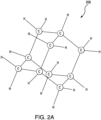
- FIGURE 2A will describe the chemical structure of an example negative electron affinity nanoparticle, adamantane diamondoid 200, according to certain embodiments.
- FIGURE 2B will describe the chemical structure of an example halogenated solution, carbon tetrachloride 205, according to certain embodiments.
- FIGURE 2C will describe an example ceramic product, polycrystalline diamond, according to certain embodiments.
- FIGURE 3 will describe a method of additive manufacture of a ceramic using a negative electron affinity nanoparticle with a halogenated solution, according to certain embodiments.
- FIGURE 4 will describe an example computer system that may be used to control the 3D printer of FIGURE 1 , according to certain embodiments.
- FIGURE 1 illustrates an example 3D printer system 100.
- 3D printer system 100 includes 3D printer 110 and laser 120.
- 3D printer 110 includes platen 130 and enclosure 140.
- Platen 130 is a plate of inert material.
- platen 130 may include platinum.
- Layers of feedstock 180 may be deposited onto platen 130 without reacting with platen 130.
- Feedstock 180 includes a negative electron affinity nanoparticle, such as adamantane diamondoid 200, and a halogenated solution, such as carbon tetrachloride 205.
- Enclosure 140 surrounds platen 130 and encloses an inert atmosphere 150. Examples of inert atmosphere 150 include nitrogen or argon gas.
- Enclosure 140 may maintain an inert 3D printing environment.
- Laser 120 is configured to raster scan feedstock 180 deposited on platen 130 to induce solvated electrons from the negative electron affinity nanoparticle, such as adamantane diamondoid 200.
- Laser 120 may emit wavelengths in the UV range.
- Laser 120 may also emit wavelengths in the visible light range.
- Laser 120 may induce a negative electron affinity nanoparticle in feedstock 180 to emit electrons into the halogenated solution, such as carbon tetrachloride 205.
- the electrons may reduce the halogen solution of feedstock 180 to form a diatomic halogen gas or liquid and an atom, such as a carbon atom.
- the carbon atom may nucleate into a ceramic, such as a diamond.
- Laser 120 may be set to certain wavelength or wavelength range.
- laser 120 may be set to a wavelength between 213 to 223 nm. As another example, laser 120 may be set to a wavelength of 532 nm. The wavelength or wavelength range may be the wavelength necessary to stimulate the emission of electrons from the negative electron affinity nanoparticle.
- 3D printer system 100 may include a control unit 160.
- Control unit 160 may include a computer system that controls the printing of an object by providing instructions to 3D printer 110.
- Control unit 160 may be either external to 3D printer 110 or incorporated into 3D printer 110. Certain embodiments of control unit 160 are discussed in more detail below with respect to FIGURE 5.
- 3D printer system 100 may include a flushing mechanism 190 configured to flush inert atmosphere 150 in enclosure 140 and to recover byproduct released into enclosure 140.
- a halogen gas byproduct may be released into enclosure 140.
- Flushing mechanism 190 may flush the halogen gas byproduct from inert atmosphere 150 of enclosure 140 and securely store the halogen gas byproduct. In this way, flushing mechanism 190 may ensure the halogen gas byproduct does not contaminate inert atmosphere 150. In this way, flushing mechanism 190 may also ensure the halogen gas byproduct is not released from 3D printing system 100 into the outside atmosphere.
- Flushing mechanism 190 may use any conventional method of flushing necessary to remove halogen gas from enclosure 140 in a way that prevents release of halogen gas into the outside atmosphere.
- flushing mechanism 190 may involve a continuous flow of argon gas through enclosure 140 and then through any conventional mechanism for recovering of halogen gas, such as by use of filters or compressors.
- 3D printer system 100 may include a draining mechanism 170 configured to drain feedstock 180.
- a draining mechanism 170 configured to drain feedstock 180.
- Draining mechanism 170 may drain the leftover feedstock 180 on platen 130 into a storage tank. Draining mechanism 170 may use any conventional method of draining necessary to remove feedstock 180 from platen 130.
- Feedstock 180 includes a halogenated solution, such as carbon tetrachloride 205.
- the halogenated solution may include bromine or chlorine as the halogen. It may be desirable to use a halogenated solution that is liquid at room temperature or at the temperature of the additive manufacture. For example, in embodiments forming a polycrystalline diamond ceramic, carbon tetrachloride or carbon tetrabromide may be liquid at room temperature. Other considerations in selecting a halogenated solution may also include the ease with which the diatomic halogen byproduct may be recovered. In some embodiments, it may be desirable for the other atoms of the halogenated solution to correspond with the atoms making up the ceramic product. For example, a halocarbon may be desirable as the halogenated solution when forming a polycrystalline diamond ceramic.
- any halocarbon may be used as the halogenated solution.
- carbon tetrachloride 205 as illustrated in FIGURE 2B may be used.
- carbon tetrabromide may be used in the halogenated solution.
- boron-nitride ceramics (dichloroamine)dichloroborane (NCl 2 -BCl 2 ) may be used as the halogenated solution and nanoparticle boron nitride as the negative electron affinity nanoparticle.
- a metal or semi-metal halogen may be added to carbon tetrachloride 205.
- a halogenated solution containing carbon and silicon such as trimethyltrichlorosilane (i.e., CCl 6 Si)
- the halogenated solution may include carbon tetrachloride 205 with the addition of silicon tetrachloride (i.e., SiCl 4 ).
- the halogenated solution may include carbon tetrachloride 205 and titanium tetrachloride (i.e., TiCl 4 ).
- the halogenated solution may include carbon tetrachloride 205 and hafnium tetrachloride (i.e., HfCl 4 ).
- the halogenated solution may include carbon tetrachloride 205 and vanadium tetrachloride (i.e., VCl 4 ).
- the halogenated solution may include carbon tetrachloride 205 and tungsten hexachloride (i.e., WCl 6 ).
- the halogenated solution may include two or more of an sp 1 carbon contributor, an sp 2 carbon contributor, and an sp 3 carbon contributor.
- the halogenated solution may include carbon tetrachloride 205 as the sp 3 contributor, and dichloroacetylene (i.e., C 2 Cl 2 ) as the sp 1 contributor.
- the halogenated solution may include carbon tetrachloride 205 as the sp 3 contributor, and tetrachloroethylene (i.e., C 2 Cl 4 ) as the sp 2 contributor.
- the halogenated solution may also include all three of an sp 1 , sp 2 , and sp 3 contributor to form a tri-hybrid-orbital-carbon ceramic.
- Feedstock 180 also includes a negative electron affinity nanoparticle.
- a negative electron affinity nanoparticle suitable to produce solvated electrons when induced by a laser, such as laser 120, may be used depending on the desired ceramic product.
- the negative electron affinity nanoparticle may act as a pseudocatalyst to produce electrons and nucleate into the ceramic.
- any diamondoid or hydrogen-terminated nanodiamond may be used as the negative electron affinity nanoparticle of feedstock 180.
- adamantane diamondoid 200 as illustrated in FIGURE 2A may be used.
- Other examples of negative electron affinity nanoparticles that may be used in forming polycrystalline diamond ceramic include diamantane and tetramantane.
- the nanodiamond or diamondoid emits electrons when illuminated by a laser, such as laser 120.
- the reduced halocarbon then nucleates on the nanodiamond or diamondoid to form diamond in sp 3 form. In this way, polycrystalline diamond ceramic is formed without the intermediary greenware, and without the need to heat an intermediary greenware in a kiln to form a final ceramic.
- an example negative electron affinity nanoparticle may include hydrogen-terminated silicon carbide nanoparticle.
- negative electron affinity boron-nitride nanoparticles may be used.
- FIGURE 2A illustrates the chemical structure of adamantane diamondoid 200 (i.e., C 10 H 16 ), which may be used as a negative electron affinity nanoparticle of feedstock 180 in certain embodiments forming a polycrystalline diamond.
- adamantane diamondoid 200 i.e., C 10 H 16
- feedstock 180 in certain embodiments forming a polycrystalline diamond.
- FIGURE 2B illustrates the chemical structure of carbon tetrachloride 205 (i.e., CCl 4 ), which may be used as a halogenated solution, according to certain embodiments.
- FIGURE 2C illustrates the chemical structure of a polycrystalline diamond (i.e., C 6 ), according to certain embodiments.
- Polycrystalline diamond is an example of a ceramic formed in certain embodiments.
- silicon carbide ceramic may be formed.
- a mixed carbon hybrid orbital ceramic may be formed.
- FIGURE 3 illustrates a method 300 for additive manufacture using a negative electron affinity nanoparticle and a halogenated solution.
- Method 300 may be implemented by 3D printer 110.
- Method 300 begins at step 305 where a film of feedstock 180 is deposited onto platen 130 of 3D printer 110.
- Feedstock 180 comprises a halogenated solution and a nanoparticle having a negative electron affinity.
- laser such as laser 120 induces the nanoparticle to emit solvated electrons into the halogenated solution to form layers of a ceramic.
- the laser inducing the nanoparticle to emit solvated electrons into the halogenated solution also forms a diatomic halogen.
- step 315 if all layers of ceramic needed to form an object have not been deposited, then 3D printer 110 will select the next cross section to be printed, and move back to step 305, where a new layer of film is deposited.
- step 310 the laser induces the nanoparticle to emit solvated electrons into the halogenated solution to form the next layer of the ceramic.
- step 315 when all layers of the ceramic needed to form the object have been printed, method 300 no longer proceeds back to step 305.
- excess feedstock 180 may be drained from the platen, such as platen 130, and into a storage tank or into a disposal tank.
- the object may be subjected to additional processing steps to prepare the object for use.
- post-printing processing may include: painting the object, polishing the object, treating the surface of the object to render it chemically inert or to make it chemically active, and assembly of another object or device from multiple printed objects.
- Method 300 may include more, fewer, or other steps. For example, steps may be performed in parallel or in any suitable order. While discussed as various components of system 100 performing the steps, any suitable component or combination of components of system 100 may perform one or more steps of the method.
- FIGURE 4 illustrates an example computer system 400 that may be used by the system of FIGURE 1 , according to certain embodiments.
- One or more computer systems 400 perform one or more steps of one or more methods described or illustrated herein.
- one or more computer systems 400 provide functionality described or illustrated herein.
- software running on one or more computer systems 400 performs one or more steps of one or more methods described or illustrated herein or provides functionality described or illustrated herein.
- Particular embodiments include one or more portions of one or more computer systems 400.
- reference to a computer system may encompass a computing device, and vice versa, where appropriate.
- reference to a computer system may encompass one or more computer systems, where appropriate.
- computer system 400 may be an embedded computer system, a system-on-chip (SOC), a single-board computer system (SBC) (such as, for example, a computer-on-module (COM) or system-on-module (SOM)), a desktop computer system, a laptop or notebook computer system, an interactive kiosk, a mainframe, a mesh of computer systems, a mobile telephone, a personal digital assistant (PDA), a server, a tablet computer system, or a combination of two or more of these.
- SOC system-on-chip
- SBC single-board computer system
- COM computer-on-module
- SOM system-on-module
- computer system 400 may include one or more computer systems 400; be unitary or distributed; span multiple locations; span multiple machines; span multiple data centers; or reside in a cloud, which may include one or more cloud components in one or more networks.
- one or more computer systems 400 may perform without substantial spatial or temporal limitation one or more steps of one or more methods described or illustrated herein.
- one or more computer systems 400 may perform in real time or in batch mode one or more steps of one or more methods described or illustrated herein.
- One or more computer systems 400 may perform at different times or at different locations one or more steps of one or more methods described or illustrated herein, where appropriate.
- computer system 400 includes a processor 402, memory 404, storage 406, an input/output (I/O) interface 408, a communication interface 410, and a bus 412.
- processor 402 memory 404
- storage 406 storage 406
- I/O interface 408 input/output (I/O) interface 408
- communication interface 410 communication interface 410
- processor 402 includes hardware for executing instructions, such as those making up a computer program.
- processor 402 may retrieve (or fetch) the instructions from an internal register, an internal cache, memory 404, or storage 406; decode and execute them; and then write one or more results to an internal register, an internal cache, memory 404, or storage 406.
- processor 402 may include one or more internal caches for data, instructions, or addresses. This disclosure contemplates processor 402 including any suitable number of any suitable internal caches, where appropriate.
- processor 402 may include one or more instruction caches, one or more data caches, and one or more translation lookaside buffers (TLBs).
- TLBs translation lookaside buffers
- Instructions in the instruction caches may be copies of instructions in memory 404 or storage 406, and the instruction caches may speed up retrieval of those instructions by processor 402.
- Data in the data caches may be copies of data in memory 404 or storage 406 for instructions executing at processor 402 to operate on; the results of previous instructions executed at processor 402 for access by subsequent instructions executing at processor 402 or for writing to memory 404 or storage 406; or other suitable data.
- the data caches may speed up read or write operations by processor 402.
- the TLBs may speed up virtual-address translation for processor 402.
- processor 402 may include one or more internal registers for data, instructions, or addresses. This disclosure contemplates processor 402 including any suitable number of any suitable internal registers, where appropriate. Where appropriate, processor 402 may include one or more arithmetic logic units (ALUs); be a multi-core processor; or include one or more processors 402. Although this disclosure describes and illustrates a particular processor, this disclosure contemplates any suitable processor.
- ALUs
- memory 404 includes main memory for storing instructions for processor 402 to execute or data for processor 402 to operate on.
- computer system 400 may load instructions from storage 406 or another source (such as, for example, another computer system 400) to memory 404.
- Processor 402 may then load the instructions from memory 404 to an internal register or internal cache.
- processor 402 may retrieve the instructions from the internal register or internal cache and decode them.
- processor 402 may write one or more results (which may be intermediate or final results) to the internal register or internal cache.
- Processor 402 may then write one or more of those results to memory 404.
- processor 402 executes only instructions in one or more internal registers or internal caches or in memory 404 (as opposed to storage 406 or elsewhere) and operates only on data in one or more internal registers or internal caches or in memory 404 (as opposed to storage 406 or elsewhere).
- One or more memory buses (which may each include an address bus and a data bus) may couple processor 402 to memory 404.
- Bus 412 may include one or more memory buses, as described below.
- one or more memory management units reside between processor 402 and memory 404 and facilitate accesses to memory 404 requested by processor 402.
- memory 404 includes random access memory (RAM).
- This RAM may be volatile memory, where appropriate Where appropriate, this RAM may be dynamic RAM (DRAM) or static RAM (SR_AM) . Moreover, where appropriate, this RAM may be single-ported or multi-ported RAM. This disclosure contemplates any suitable RAM.
- Memory 404 may include one or more memories 404, where appropriate. Although this disclosure describes and illustrates particular memory, this disclosure contemplates any suitable memory.
- storage 406 includes mass storage for data or instructions.
- storage 406 may include a hard disk drive (HDD), a floppy disk drive, flash memory, an optical disc, a magneto-optical disc, magnetic tape, or a Universal Serial Bus (USB) drive or a combination of two or more of these.
- Storage 406 may include removable or non-removable (or fixed) media, where appropriate.
- Storage 406 may be internal or external to computer system 400, where appropriate.
- storage 406 is non-volatile, solid-state memory.
- storage 406 includes read-only memory (ROM).
- this ROM may be mask-programmed ROM, programmable ROM (PROM), erasable PROM (EPROM), electrically erasable PROM (EEPROM), electrically alterable ROM (EAROM), or flash memory or a combination of two or more of these.
- This disclosure contemplates mass storage 406 taking any suitable physical form.
- Storage 406 may include one or more storage control units facilitating communication between processor 402 and storage 406, where appropriate. Where appropriate, storage 406 may include one or more storages 406. Although this disclosure describes and illustrates particular storage, this disclosure contemplates any suitable storage.
- I/O interface 408 includes hardware, software, or both, providing one or more interfaces for communication between computer system 400 and one or more I/O devices.
- Computer system 400 may include one or more of these I/O devices, where appropriate.
- One or more of these I/O devices may enable communication between a person and computer system 400.
- an I/O device may include a keyboard, keypad, microphone, monitor, mouse, printer, scanner, speaker, still camera, stylus, tablet, touch screen, trackball, video camera, another suitable I/O device or a combination of two or more of these.
- An I/O device may include one or more sensors. This disclosure contemplates any suitable I/O devices and any suitable I/O interfaces 408 for them.
- I/O interface 408 may include one or more device or software drivers enabling processor 402 to drive one or more of these I/O devices.
- I/O interface 408 may include one or more I/O interfaces 408, where appropriate.
- communication interface 410 includes hardware, software, or both providing one or more interfaces for communication (such as, for example, packet-based communication) between computer system 400 and one or more other computer systems 400 or one or more networks.
- communication interface 410 may include a network interface controller (NIC) or network adapter for communicating with an Ethernet or other wire-based network or a wireless NIC (WNIC) or wireless adapter for communicating with a wireless network, such as a WI-FI network.
- NIC network interface controller
- WNIC wireless NIC
- WI-FI network wireless network
- computer system 400 may communicate with an ad hoc network, a personal area network (PAN), a local area network (LAN), a wide area network (WAN), a metropolitan area network (MAN), or one or more portions of the Internet or a combination of two or more of these.
- PAN personal area network
- LAN local area network
- WAN wide area network
- MAN metropolitan area network
- computer system 400 may communicate with a wireless PAN (WPAN) (such as, for example, a BLUETOOTH WPAN), a WI-FI network, a WI-MAX network, a cellular telephone network (such as, for example, a Global System for Mobile Communications (GSM) network), or other suitable wireless network or a combination of two or more of these.
- WPAN wireless PAN
- WI-FI wireless personal area network
- WI-MAX wireless personal area network
- WI-MAX wireless personal area network
- cellular telephone network such as, for example, a Global System for Mobile Communications (GSM) network
- GSM Global System
- bus 412 includes hardware, software, or both coupling components of computer system 400 to each other.
- bus 412 may include an Accelerated Graphics Port (AGP) or other graphics bus, an Enhanced Industry Standard Architecture (EISA) bus, a front-side bus (FSB), a HYPERTRANSPORT (HT) interconnect, an Industry Standard Architecture (ISA) bus, an INFINIBAND interconnect, a low-pin-count (LPC) bus, a memory bus, a Micro Channel Architecture (MCA) bus, a Peripheral Component Interconnect (PCI) bus, a PCI-Express (PCIe) bus, a serial advanced technology attachment (SATA) bus, a Video Electronics Standards Association local (VLB) bus, or another suitable bus or a combination of two or more of these.
- Bus 412 may include one or more buses 412, where appropriate.
- the components of computer system 400 may be integrated or separated. In some embodiments, components of computer system 400 may each be housed within a single chassis. The operations of computer system 400 may be performed by more, fewer, or other components. Additionally, operations of computer system 400 may be performed using any suitable logic that may comprise software, hardware, other logic, or any suitable combination of the preceding.
- a computer-readable non-transitory storage medium or media may include one or more semiconductor-based or other integrated circuits (ICs) (such, as for example, fieldprogrammable gate arrays (FPGAs) or application-specific ICs (ASICs)), hard disk drives (HDDs), hybrid hard drives (HHDs), optical discs, optical disc drives (ODDs), magneto-optical discs, magneto-optical drives, floppy diskettes, floppy disk drives (FDDs), magnetic tapes, solid-state drives (SSDs), RAMdrives, SECURE DIGITAL cards or drives, any other suitable computer-readable non-transitory storage media, or any suitable combination of two or more of these, where appropriate.
- ICs semiconductor-based or other integrated circuits
- HDDs hard disk drives
- HHDs hybrid hard drives
- ODDs optical disc drives
- magneto-optical discs magneto-optical drives
- FDDs floppy diskettes
- FDDs floppy disk drives
- SSDs solid-
Landscapes
- Chemical & Material Sciences (AREA)
- Engineering & Computer Science (AREA)
- Organic Chemistry (AREA)
- Materials Engineering (AREA)
- Manufacturing & Machinery (AREA)
- Ceramic Engineering (AREA)
- Chemical Kinetics & Catalysis (AREA)
- Structural Engineering (AREA)
- Life Sciences & Earth Sciences (AREA)
- Inorganic Chemistry (AREA)
- General Chemical & Material Sciences (AREA)
- Mechanical Engineering (AREA)
- Wood Science & Technology (AREA)
- Physics & Mathematics (AREA)
- Optics & Photonics (AREA)
- General Life Sciences & Earth Sciences (AREA)
- Geology (AREA)
- Metallurgy (AREA)
- Crystallography & Structural Chemistry (AREA)
- Plasma & Fusion (AREA)
- Producing Shaped Articles From Materials (AREA)
- Carbon And Carbon Compounds (AREA)
- Powder Metallurgy (AREA)
Applications Claiming Priority (2)
| Application Number | Priority Date | Filing Date | Title |
|---|---|---|---|
| US15/976,626 US10960571B2 (en) | 2018-05-10 | 2018-05-10 | Direct additive synthesis from UV-induced solvated electrons in feedstock of halogenated material and negative electron affinity nanoparticle |
| EP19173744.4A EP3566871B1 (de) | 2018-05-10 | 2019-05-10 | Direkte additive synthese aus uv-induzierten solvatisierten elektronen in rohstoffen aus halogeniertem material und nanopartikeln mit negativelektronenaffinität |
Related Parent Applications (2)
| Application Number | Title | Priority Date | Filing Date |
|---|---|---|---|
| EP19173744.4A Division EP3566871B1 (de) | 2018-05-10 | 2019-05-10 | Direkte additive synthese aus uv-induzierten solvatisierten elektronen in rohstoffen aus halogeniertem material und nanopartikeln mit negativelektronenaffinität |
| EP19173744.4A Division-Into EP3566871B1 (de) | 2018-05-10 | 2019-05-10 | Direkte additive synthese aus uv-induzierten solvatisierten elektronen in rohstoffen aus halogeniertem material und nanopartikeln mit negativelektronenaffinität |
Publications (3)
| Publication Number | Publication Date |
|---|---|
| EP4467341A2 true EP4467341A2 (de) | 2024-11-27 |
| EP4467341A3 EP4467341A3 (de) | 2025-03-05 |
| EP4467341B1 EP4467341B1 (de) | 2026-03-18 |
Family
ID=66483888
Family Applications (2)
| Application Number | Title | Priority Date | Filing Date |
|---|---|---|---|
| EP24206381.6A Active EP4467341B1 (de) | 2018-05-10 | 2019-05-10 | Ein system für die direkte generative synthese aus uv-induzierten solvatisierten elektronen in einem ausgangsstoff für halogeniertes material und nanopartikel mit negativer elektronenaffinität |
| EP19173744.4A Active EP3566871B1 (de) | 2018-05-10 | 2019-05-10 | Direkte additive synthese aus uv-induzierten solvatisierten elektronen in rohstoffen aus halogeniertem material und nanopartikeln mit negativelektronenaffinität |
Family Applications After (1)
| Application Number | Title | Priority Date | Filing Date |
|---|---|---|---|
| EP19173744.4A Active EP3566871B1 (de) | 2018-05-10 | 2019-05-10 | Direkte additive synthese aus uv-induzierten solvatisierten elektronen in rohstoffen aus halogeniertem material und nanopartikeln mit negativelektronenaffinität |
Country Status (3)
| Country | Link |
|---|---|
| US (2) | US10960571B2 (de) |
| EP (2) | EP4467341B1 (de) |
| JP (2) | JP6951376B2 (de) |
Families Citing this family (2)
| Publication number | Priority date | Publication date | Assignee | Title |
|---|---|---|---|---|
| US11052647B2 (en) * | 2018-05-10 | 2021-07-06 | Lockheed Martin Corporation | Direct additive synthesis of diamond semiconductor |
| US11865809B2 (en) * | 2019-08-22 | 2024-01-09 | The Boeing Company | Method for forming non-bonded regions in multi-layered metallic armor |
Family Cites Families (30)
| Publication number | Priority date | Publication date | Assignee | Title |
|---|---|---|---|---|
| US5053434A (en) | 1989-10-25 | 1991-10-01 | Mobil Oil Corporation | Diamondoid polymeric compositions |
| JPH04209797A (ja) * | 1990-11-30 | 1992-07-31 | Sumitomo Electric Ind Ltd | ダイヤモンド合成方法 |
| JPH0543393A (ja) * | 1991-08-16 | 1993-02-23 | Semiconductor Energy Lab Co Ltd | 炭素材料作製方法 |
| US5463018A (en) | 1993-11-15 | 1995-10-31 | Board Of Regents Of The University Of Nebraska | Preparation of doped polycarbynes |
| US5436315A (en) | 1993-11-15 | 1995-07-25 | Board Of Regents Of The University Of Nebraska | Preparations of polycarbynes |
| US5516884A (en) * | 1994-03-09 | 1996-05-14 | The Penn State Research Foundation | Preparation of polycarbynes and diamond-like carbon materials made therefrom |
| JP2000273632A (ja) | 1999-03-25 | 2000-10-03 | Ibiden Co Ltd | 化学気相蒸着法により反りの無いフラットなセラミックバルク材料を製造する方法 |
| TWI228114B (en) | 1999-12-24 | 2005-02-21 | Nat Science Council | Method and equipment for making ceramic work piece |
| JP4264235B2 (ja) | 2002-08-16 | 2009-05-13 | 聡 河田 | 3次元フォトニック結晶を形成する方法 |
| KR100618878B1 (ko) * | 2004-11-26 | 2006-09-04 | 삼성전자주식회사 | 사면체 탄소 화합물로 이루어지는 하드 마스크용 폴리머막및 그 제조 방법과 이를 이용한 미세 패턴 형성 방법 |
| JP5047284B2 (ja) * | 2006-07-17 | 2012-10-10 | カミル トッパレ,レヴェント | ダイヤモンドおよびダイヤモンド状セラミックのポリマー前駆体であるポリカルビンの製造のための新たな工業的に実行可能な方法 |
| US7547358B1 (en) | 2008-03-03 | 2009-06-16 | Shapiro Zalman M | System and method for diamond deposition using a liquid-solvent carbon-transfer mechanism |
| US8252263B2 (en) | 2008-04-14 | 2012-08-28 | Chien-Min Sung | Device and method for growing diamond in a liquid phase |
| WO2012103622A1 (en) | 2011-02-02 | 2012-08-09 | Epic Ventures Inc. | Method for making poly(hydridocarbyne) |
| US9944021B2 (en) | 2012-03-02 | 2018-04-17 | Dynamic Material Systems, LLC | Additive manufacturing 3D printing of advanced ceramics |
| KR101858799B1 (ko) * | 2013-03-15 | 2018-05-16 | 웨스트 버지니아 유니버시티 리서치 코포레이션 | 순수한 탄소 제조 공정, 그 조성물 및 방법 |
| WO2015023612A2 (en) | 2013-08-15 | 2015-02-19 | Oxane Materials, Inc. | Additive fabrication of proppants |
| US9302945B2 (en) * | 2014-03-07 | 2016-04-05 | Lockheed Martin Corporation | 3-D diamond printing using a pre-ceramic polymer with a nanoparticle filler |
| US9643361B2 (en) | 2014-05-27 | 2017-05-09 | Jian Liu | Method and apparatus for three-dimensional additive manufacturing with a high energy high power ultrafast laser |
| GB2546016B (en) * | 2014-06-20 | 2018-11-28 | Velo3D Inc | Apparatuses, systems and methods for three-dimensional printing |
| US10300624B2 (en) | 2014-10-17 | 2019-05-28 | United Technologies Corporation | Functional inorganics and ceramic additive manufacturing |
| US9402322B1 (en) | 2015-03-04 | 2016-07-26 | Lockheed Martin Corporation | Metal-free monolithic epitaxial graphene-on-diamond PWB with optical waveguide |
| US11691341B2 (en) | 2015-10-30 | 2023-07-04 | Seurat Technologies, Inc. | Part manipulation using printed manipulation points |
| TW201726367A (zh) | 2016-01-05 | 2017-08-01 | 應用材料股份有限公司 | 三維列印之材料及配方 |
| US10994371B2 (en) | 2016-02-24 | 2021-05-04 | Mitsubishi Electric Research Laboratories, Inc. | System and method for depositing a metal to form a three-dimensional part |
| EP3442772A4 (de) | 2016-04-14 | 2019-11-13 | Desktop Metal, Inc. | Generative fertigung mit stützstrukturen |
| CN105788891A (zh) | 2016-04-29 | 2016-07-20 | 河南省豫星华晶微钻有限公司 | 一种基于3d打印技术的高耐磨高导热电触头及制备工艺 |
| CN106449809B (zh) | 2016-11-21 | 2018-06-08 | 北方民族大学 | 基于3d打印纳米金刚石透明薄膜电池的家用玻璃及制备方法 |
| US10577249B2 (en) * | 2017-05-12 | 2020-03-03 | Lockheed Martin Corporation | Tailorable polyorbital-hybrid ceramics |
| US11052647B2 (en) * | 2018-05-10 | 2021-07-06 | Lockheed Martin Corporation | Direct additive synthesis of diamond semiconductor |
-
2018
- 2018-05-10 US US15/976,626 patent/US10960571B2/en active Active
-
2019
- 2019-05-09 JP JP2019088808A patent/JP6951376B2/ja active Active
- 2019-05-10 EP EP24206381.6A patent/EP4467341B1/de active Active
- 2019-05-10 EP EP19173744.4A patent/EP3566871B1/de active Active
-
2021
- 2021-03-02 US US17/189,702 patent/US11670507B2/en active Active
- 2021-09-24 JP JP2021155072A patent/JP7190012B2/ja active Active
Also Published As
| Publication number | Publication date |
|---|---|
| EP4467341A3 (de) | 2025-03-05 |
| JP7190012B2 (ja) | 2022-12-14 |
| EP3566871A1 (de) | 2019-11-13 |
| US10960571B2 (en) | 2021-03-30 |
| US20210206020A1 (en) | 2021-07-08 |
| US20190344470A1 (en) | 2019-11-14 |
| JP2019196008A (ja) | 2019-11-14 |
| US11670507B2 (en) | 2023-06-06 |
| JP6951376B2 (ja) | 2021-10-20 |
| EP4467341B1 (de) | 2026-03-18 |
| JP2022008517A (ja) | 2022-01-13 |
| EP3566871B1 (de) | 2024-12-25 |
Similar Documents
| Publication | Publication Date | Title |
|---|---|---|
| US9302945B2 (en) | 3-D diamond printing using a pre-ceramic polymer with a nanoparticle filler | |
| US9402322B1 (en) | Metal-free monolithic epitaxial graphene-on-diamond PWB with optical waveguide | |
| US9504158B2 (en) | Metal-free monolithic epitaxial graphene-on-diamond PWB | |
| US11670507B2 (en) | Direct additive synthesis from UV-induced solvated electrons in feedstock of halogenated material and negative electron affinity nanoparticle | |
| US11557475B2 (en) | Direct additive synthesis of diamond semiconductor | |
| US20150301281A1 (en) | Metal-Free Monolithic Epitaxial Graphene-On-Diamond PWB With Optical Waveguide | |
| US12454075B2 (en) | Additive manufacture of complex intermetallic and ceramic structures | |
| Palanki et al. | Fabrication of thorium and thorium dioxide | |
| JP2019196008A5 (de) | ||
| Lin et al. | The effect of yttrium incorporation on the formation and properties of α-Al2O3 coatings |
Legal Events
| Date | Code | Title | Description |
|---|---|---|---|
| PUAI | Public reference made under article 153(3) epc to a published international application that has entered the european phase |
Free format text: ORIGINAL CODE: 0009012 |
|
| STAA | Information on the status of an ep patent application or granted ep patent |
Free format text: STATUS: REQUEST FOR EXAMINATION WAS MADE |
|
| 17P | Request for examination filed |
Effective date: 20241014 |
|
| AC | Divisional application: reference to earlier application |
Ref document number: 3566871 Country of ref document: EP Kind code of ref document: P |
|
| AK | Designated contracting states |
Kind code of ref document: A2 Designated state(s): AL AT BE BG CH CY CZ DE DK EE ES FI FR GB GR HR HU IE IS IT LI LT LU LV MC MK MT NL NO PL PT RO RS SE SI SK SM TR |
|
| REG | Reference to a national code |
Ref country code: DE Ref legal event code: R079 Free format text: PREVIOUS MAIN CLASS: B33Y0070000000 Ipc: B33Y0010000000 Ref country code: DE Ref legal event code: R079 Ref document number: 602019082760 Country of ref document: DE Free format text: PREVIOUS MAIN CLASS: B33Y0070000000 Ipc: B33Y0010000000 |
|
| PUAL | Search report despatched |
Free format text: ORIGINAL CODE: 0009013 |
|
| AK | Designated contracting states |
Kind code of ref document: A3 Designated state(s): AL AT BE BG CH CY CZ DE DK EE ES FI FR GB GR HR HU IE IS IT LI LT LU LV MC MK MT NL NO PL PT RO RS SE SI SK SM TR |
|
| RIC1 | Information provided on ipc code assigned before grant |
Ipc: B33Y 70/00 20200101ALI20250124BHEP Ipc: C04B 35/573 20060101ALI20250124BHEP Ipc: C04B 35/56 20060101ALI20250124BHEP Ipc: C04B 35/528 20060101ALI20250124BHEP Ipc: B23K 26/342 20140101ALI20250124BHEP Ipc: C04B 35/622 20060101ALI20250124BHEP Ipc: B32B 18/00 20060101ALI20250124BHEP Ipc: B28B 1/00 20060101ALI20250124BHEP Ipc: B29C 64/393 20170101ALI20250124BHEP Ipc: B29C 64/135 20170101ALI20250124BHEP Ipc: B33Y 30/00 20150101ALI20250124BHEP Ipc: B33Y 10/00 20150101AFI20250124BHEP |
|
| STAA | Information on the status of an ep patent application or granted ep patent |
Free format text: STATUS: EXAMINATION IS IN PROGRESS |
|
| 17Q | First examination report despatched |
Effective date: 20250814 |
|
| GRAP | Despatch of communication of intention to grant a patent |
Free format text: ORIGINAL CODE: EPIDOSNIGR1 |
|
| STAA | Information on the status of an ep patent application or granted ep patent |
Free format text: STATUS: GRANT OF PATENT IS INTENDED |
|
| INTG | Intention to grant announced |
Effective date: 20251107 |
|
| P01 | Opt-out of the competence of the unified patent court (upc) registered |
Free format text: CASE NUMBER: UPC_APP_0013817_4467341/2025 Effective date: 20251119 |
|
| GRAS | Grant fee paid |
Free format text: ORIGINAL CODE: EPIDOSNIGR3 |
|
| GRAA | (expected) grant |
Free format text: ORIGINAL CODE: 0009210 |
|
| STAA | Information on the status of an ep patent application or granted ep patent |
Free format text: STATUS: THE PATENT HAS BEEN GRANTED |
|
| AC | Divisional application: reference to earlier application |
Ref document number: 3566871 Country of ref document: EP Kind code of ref document: P |
|
| AK | Designated contracting states |
Kind code of ref document: B1 Designated state(s): AL AT BE BG CH CY CZ DE DK EE ES FI FR GB GR HR HU IE IS IT LI LT LU LV MC MK MT NL NO PL PT RO RS SE SI SK SM TR |
|
| REG | Reference to a national code |
Ref country code: CH Ref legal event code: F10 Free format text: ST27 STATUS EVENT CODE: U-0-0-F10-F00 (AS PROVIDED BY THE NATIONAL OFFICE) Effective date: 20260318 Ref country code: GB Ref legal event code: FG4D |
|
| REG | Reference to a national code |
Ref country code: DE Ref legal event code: R096 Ref document number: 602019082760 Country of ref document: DE |
|
| REG | Reference to a national code |
Ref country code: IE Ref legal event code: FG4D |