EP4462599A1 - Air-strip line and antenna device comprising air-strip line - Google Patents
Air-strip line and antenna device comprising air-strip line Download PDFInfo
- Publication number
- EP4462599A1 EP4462599A1 EP23737460.8A EP23737460A EP4462599A1 EP 4462599 A1 EP4462599 A1 EP 4462599A1 EP 23737460 A EP23737460 A EP 23737460A EP 4462599 A1 EP4462599 A1 EP 4462599A1
- Authority
- EP
- European Patent Office
- Prior art keywords
- feed line
- dielectric plate
- groove
- antenna device
- plate
- Prior art date
- Legal status (The legal status is an assumption and is not a legal conclusion. Google has not performed a legal analysis and makes no representation as to the accuracy of the status listed.)
- Pending
Links
Images



Classifications
-
- H—ELECTRICITY
- H01—ELECTRIC ELEMENTS
- H01Q—ANTENNAS, i.e. RADIO AERIALS
- H01Q21/00—Antenna arrays or systems
- H01Q21/0087—Apparatus or processes specially adapted for manufacturing antenna arrays
-
- H—ELECTRICITY
- H01—ELECTRIC ELEMENTS
- H01Q—ANTENNAS, i.e. RADIO AERIALS
- H01Q21/00—Antenna arrays or systems
- H01Q21/06—Arrays of individually energised antenna units similarly polarised and spaced apart
- H01Q21/061—Two dimensional planar arrays
- H01Q21/065—Patch antenna array
-
- H—ELECTRICITY
- H01—ELECTRIC ELEMENTS
- H01P—WAVEGUIDES; RESONATORS, LINES, OR OTHER DEVICES OF THE WAVEGUIDE TYPE
- H01P3/00—Waveguides; Transmission lines of the waveguide type
- H01P3/02—Waveguides; Transmission lines of the waveguide type with two longitudinal conductors
- H01P3/08—Microstrips; Strip lines
- H01P3/081—Microstriplines
- H01P3/084—Suspended microstriplines
-
- H—ELECTRICITY
- H01—ELECTRIC ELEMENTS
- H01Q—ANTENNAS, i.e. RADIO AERIALS
- H01Q1/00—Details of, or arrangements associated with, antennas
- H01Q1/42—Housings not intimately mechanically associated with radiating elements, e.g. radome
- H01Q1/422—Housings not intimately mechanically associated with radiating elements, e.g. radome comprising two or more layers of dielectric material
-
- H—ELECTRICITY
- H01—ELECTRIC ELEMENTS
- H01Q—ANTENNAS, i.e. RADIO AERIALS
- H01Q21/00—Antenna arrays or systems
- H01Q21/0006—Particular feeding systems
- H01Q21/0075—Stripline fed arrays
- H01Q21/0081—Stripline fed arrays using suspended striplines
-
- H—ELECTRICITY
- H01—ELECTRIC ELEMENTS
- H01Q—ANTENNAS, i.e. RADIO AERIALS
- H01Q21/00—Antenna arrays or systems
- H01Q21/24—Combinations of antenna units polarised in different directions for transmitting or receiving circularly and elliptically polarised waves or waves linearly polarised in any direction
-
- H—ELECTRICITY
- H01—ELECTRIC ELEMENTS
- H01Q—ANTENNAS, i.e. RADIO AERIALS
- H01Q9/00—Electrically-short antennas having dimensions not more than twice the operating wavelength and consisting of conductive active radiating elements
- H01Q9/04—Resonant antennas
- H01Q9/0407—Substantially flat resonant element parallel to ground plane, e.g. patch antenna
- H01Q9/045—Substantially flat resonant element parallel to ground plane, e.g. patch antenna with particular feeding means
- H01Q9/0457—Substantially flat resonant element parallel to ground plane, e.g. patch antenna with particular feeding means electromagnetically coupled to the feed line
-
- H—ELECTRICITY
- H01—ELECTRIC ELEMENTS
- H01Q—ANTENNAS, i.e. RADIO AERIALS
- H01Q9/00—Electrically-short antennas having dimensions not more than twice the operating wavelength and consisting of conductive active radiating elements
- H01Q9/04—Resonant antennas
- H01Q9/0485—Dielectric resonator antennas
Definitions
- the present disclosure relates to an air-strip line and an antenna device including the air-strip line.
- the antenna device may include a plate, a radiation element, and a feed line that supplies power to the radiation element.
- the size of the radiation element may vary depending on the frequency of use. For example, as the operating frequency increases, the size of the radiation element decreases.
- Multiple feed lines may be printed in a pattern on a substrate.
- the substrate is made of a PCB material (for example, FR4 material) with a predetermined dielectric constant, the insertion loss due to the multiple pattern-printed feed lines increases, which deteriorates the performance of the antenna device.
- Loss due to feed lines can be divided into conductor loss in the conductor through which the signal flows and dielectric loss due to the dielectric surrounding the conductor.
- the loss directly reduces the gain of the antenna device.
- it is necessary to improve the loss, and since changing or deforming the medium is relatively advantageous, improving the dielectric loss is effective.
- a representative example of the feed line used to improve dielectric loss is an air-strip line structure.
- the air-strip line structure refers to a feed line structure in which the dielectric portion is implemented as air.
- the dielectric loss In a feed line of the air-strip line structure, the dielectric loss is close to 0 because the conductor is surrounded by air. Therefore, when using a feed line of the air-strip line structure, the dielectric loss can be reduced, which increases the gain of the antenna device.
- the impedance can be varied by adjusting the width of the feed line.
- the width of the feed line is wider for the same impedance compared to the PCB type, so adjusting the width of the feed line to vary the impedance has limitations in the design of the antenna device.
- a height difference may occur between the feed lines during processing, and the characteristics of the antenna device may be deteriorated due to the height difference.
- the present disclosure provides an antenna device capable of adjusting the distance between a feed line and a dielectric plate and the thickness of the dielectric plate.
- the present disclosure provides an antenna device capable of configuring a circuit by changing only the structure of the dielectric while reducing the change in the width of the feed line.
- an antenna device comprising: a plate; a first dielectric plate coupled to one surface of the plate; a plurality of radiation elements arranged along a first direction on the first dielectric plate; and a plurality of first feed lines configured to supply power to the plurality of radiation elements and having an air-strip line structure, wherein the first dielectric plate includes a first groove penetrating upper and lower surfaces of the first dielectric plate and configured to allow the first feed line to float therein, and the first feed line is configured to float in the first groove.
- a feed line of an air-strip line structure which supplies power to a radiation element of an antenna device, the feed line comprising: a dielectric plate; a groove formed to penetrate through upper and lower surfaces of the dielectric plate; and a line unit configured to float at a predetermined distance from a side wall of the groove.
- the antenna device can vary the impedance by adjusting the distance between the feed line and the dielectric plate and the thickness of the dielectric plate.
- the antenna device can minimize the height difference that occurs when manufacturing the feed line by reducing the change in the width of the feed line.
- upper surface or “upper portion” refers to the direction in which radiation elements 14, 24 are coupled in antenna devices 1, 2, and “bottom surface” or “bottom portion” refers to the direction in which plates 11, 21 are coupled in the antenna devices 1, 2.
- FIG. 1 is a combined perspective view of an antenna device according to one embodiment of the present disclosure.
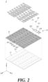
- FIG.2 is an exploded perspective view of the antenna device according to one embodiment of the present disclosure.
- an antenna device 1 may include all or some of a plate 11, a first dielectric plate 12, a first feed line 13, and a plurality of radiation elements 14.
- the first dielectric plate 12 may be coupled to an upper surface of the plate 11.
- the plate 11 may be made of a metallic material and may provide a ground plane for the radiation elements 14 of the antenna device 1.
- the plate 11 may include a plurality of holes 111.
- the plurality of holes 111 may be formed to penetrate the plate 11.
- the plurality of holes 111 may include a plurality of first holes and a plurality of second holes. Protrusions (not shown) of the first dielectric plate 12 are inserted into the plurality of first holes, so that the plate 11 and the first dielectric plate 12 can be coupled.
- RF filters, connectors, ports, etc. may be coupled in the plurality of second holes to be connected to the antenna device 1.
- the first dielectric plate 12 may include all or some of a first groove 121, a second groove 122, a first support unit 123, a first connection unit 124, a second connection unit 125, and a protrusion (not shown).
- the first dielectric plate 12 may be formed on the upper surface of the plate 11 through injection.
- all or some of the components of the first dielectric plate 12, the first groove 121, the second groove 122, the first support unit 123, the first connection unit 124, the second connection unit 125, and the protrusions may be formed integrally.
- the first dielectric plate 12 may be made of a dielectric, e.g., plastic material.
- the first groove 121 may be formed to penetrate the upper and lower surfaces of the first dielectric plate 12.
- the first groove 121 may extend longitudinally along a first direction.
- the first direction is a direction parallel to the Y-axis of FIG. 1 .
- the first groove 121 may be formed to correspond to the shape of the first feed line 13, which will be described later, so that the first feed line 13 can float in the first groove 121.
- the first feed line 13 may be configured to float in the first groove 121.
- the first feed line 13 may float at a predetermined distance from the side wall of the first groove 121.
- the first feed line 13 may float at a predetermined distance from the plate 11 coupled to the lower surface of the first dielectric plate 12.
- the space between the first feed line 13 and the side wall of the first groove 121 and/or the plate 11 may be filled with air. That is, the first feed line 13 may have an air-strip line structure.
- the air-strip line structure refers to a structure in which the dielectric portion is implemented as air in a general stripline structure.
- the dielectric loss is close to '0' because the conductor is surrounded by air. Therefore, the gain of the antenna device 1 can be increased by reducing the dielectric loss.
- the first support unit 123 may be formed in the first groove 121.
- the first support unit 123 is formed at the bottom of the first groove 121 and may connect opposing side walls of the first groove 121.
- the first support unit 123 may be connected to the first groove 121 and formed integrally with the first dielectric plate 12, but a thickness of the first support unit 123 may be thinner than a thickness of the first groove 121.
- the first support unit 123 may be formed in the first groove 121 at predetermined intervals along the first direction.
- the first feed line 13 may be coupled to upper surfaces of a plurality of first support units 123 formed at predetermined intervals. As the first feed line 13 is coupled to the upper surfaces of the first support unit 123, the first feed line 13 may float at a predetermined distance from the side wall of the first groove 121 and/or the plate 11. That is, by using the first support unit 123, an air-strip line structure can be formed using only a minimum amount of dielectric.
- the second groove 122 may be formed in at least a portion of the first dielectric plate 12 where the first groove 121 is not formed.
- the second groove 122 may be formed to penetrate the upper and lower surfaces of the first dielectric plate 12.
- the second groove 122 may be formed regularly with a predetermined pattern.
- the second groove 122 may be formed in a honeycomb-shaped pattern.
- the present disclosure is not limited to the above, and the second groove 122 may be formed irregularly.
- the first connection unit 124 may be formed to protrude from the upper surface of the first dielectric plate 12.
- the first connection unit 124 may connect the first dielectric plate 12 and the radiation element 14.
- Four first connection units 124 may be formed at predetermined intervals to connect the first dielectric plate 12 and the radiation element 14.
- the four first connection units 124 may be arranged to form a square shape.
- the present disclosure is not limited to the above, and the number and arrangement of the first connection units 124 may be designed in various ways as needed.
- the second connection unit 125 may be formed to protrude from the upper surface of the first dielectric plate 12 .
- the second connection unit 125 may connect the first dielectric plate 12 and the first feed line 13.
- the second connection unit 125 may be formed below the radiation element 14 so that the first feed line 13 can feed the radiation element 14. That is, the height of the second connection unit 125 may be lower than the height of the first connection unit 124.
- the second connection units 125 may be formed as a pair.
- the present disclosure is not limited to the above, and the number and arrangement of the second connection units 125 may be designed in various ways as needed.
- the protrusion may be formed on the lower surface of the first dielectric plate 12.
- the protrusion is formed to protrude from the lower surface of the first dielectric plate 12 and can be inserted into the hole 111 of the plate 11.
- the first dielectric plate 12 and the plate 11 may be coupled by inserting the protrusions into the holes 111.
- a plurality of protrusions may be formed corresponding to the positions of the holes 111 of the plate 11.
- the plurality of protrusions may be formed integrally with the first dielectric plate 12.
- a plurality of radiation elements 14 may be arranged in a row along the first direction.
- the plurality of radiation elements 14 may form one antenna column.
- the first direction is a direction parallel to the Y-axis of FIG. 1 .
- the intermediate frequency of the operating frequency band is lambda
- the gap between one radiation element 14 and its neighboring radiation element 14 is equal to or more than 1 lambda, undesirable grating lobes may occur in the radiation pattern.
- the gap between one radiation element 14 and its neighboring radiation element 14 in the first direction is less than 1 lambda.
- the present disclosure is not limited to the above, and the gap in the first direction between the two radiation elements 14 may have a value outside the above-described range.
- the antenna device 1 may include a plurality of antenna columns.
- a plurality of antenna columns may be arranged on the plate 11 along a second direction perpendicular to the first direction.
- the second direction is a direction parallel to the X-axis of FIG. 1 .
- the plurality of radiation elements 14 may be configured to implement dual polarization.
- the first feed line 13 may be configured as a pair so that the radiation element 14 implements dual polarization.
- the pair of first feed lines 13 may be arranged symmetrically. For example, two types of polarized signals of +45 degrees and -45 degrees may be radiated from one radiation element 14.
- the present disclosure is not limited to the above, and the radiation element 14 may be configured to implement single polarization or quadruple polarization.
- the first feed line 13 may be configured to supply power to a plurality of radiation elements 14. That is, the plurality of radiation elements 14 can transmit and receive signals or receive power using the first feed line 13.
- the first feed line 13 may include a main line region 131, a connection line region 132, and an input/output region 133.
- the main line region 131 may extend longitudinally along the first direction.
- the connection line region 132 may have one end connected to the second connection unit 125 and the other end connected to the main line region 131.
- the connection line region 132 may be formed by bending the main line region 131 at a predetermined angle.
- the connection line region 132 may be formed by bending the main line region 131 into an 'L' shape.
- the present disclosure is not limited to the above, and the connection line region 132 may be formed obliquely.
- connection line region 132 may be branched from the main line region 131, and each connection line region 132 may be connected to the corresponding radiation element 14.
- the connection line region 132 may be directly connected to the radiation element 14, or may be connected by a coupling method.
- the input/output region 133 may be branched from the main line region 131 and may connect an RF circuit to the main line region 131.
- One end of the input/output region 133 may be connected to the main line region 131, and the other end of the input/output region 133 may be connected to the RF circuit provided with a filter, a power amplifier, a power supply unit, and the like.
- the RF circuit may be provided inside the antenna device 1, but may also be provided in an external device outside the antenna device 1, for example, a remote radio head (RRH).
- a remote radio head RRH
- the antenna device 1 and the external device with the RF circuit may be connected using an RF cable, a connector, or the like.
- the input/output region 133 may transmit signals transmitted from the RF circuit to the plurality of radiation elements 14 or transmit signals received them from the plurality of radiation elements 14 to the RF circuit, using the main line region 131 and the connection line region 132. In addition, the input/output region 133 may supply power to the plurality of radiation elements 14 using the main line region 131 and the connection line region 132.
- the input/output region 133 may be disposed near the middle portion of the main line region 131.
- the dielectric portion is implemented as air, so the length of the first feed line 13 for inputting the same phase to the plurality of radiation elements 14 may be relatively long.
- the length of the first feed line 13 required to input signals of the same phase to the first radiation element and the second radiation element adjacent to the first radiation element may be 1 lambda. That is, the length of the first feed line 13 from the first connection line region and the second connection line region adjacent to the first connection line region may be 1 lambda.
- the gap in the first direction between two adjacent radiation elements 14 is preferably less than 1 lambda.
- the length of the first feed line connecting the two adjacent radiation elements 14 may be longer than the gap between the two adjacent radiation elements 14, which may be a problem.
- the main line region 131 may include a delay line.
- the delay line may be formed in at least a portion of the main line region 131.
- the delay line may be an area formed by bending a portion of the main line region 131, and may partially compensate for the length of the first feed line 13, which has become longer.
- the delay line may have a concave shape or a convex shape toward the other first feed line 13.
- the delay line may have a 'C' shape, but the present disclosure is not limited thereto.
- the antenna device 1 With the main line region 131 including the delay line, the distance between the two adjacent radiation elements 14 in the first direction can be prevented from inevitably increasing. Accordingly, the antenna device 1 can be compact, and the occurrence of undesirable grating lobes can be minimized.
- FIG. 3 is an enlarged top view of part B of FIG. 1 .
- the first feed line 13 of the antenna device 1 of the present disclosure may be configured to float in the first groove 121.
- the first feed line 13 may float at a predetermined distance from the side wall of the first groove 121.
- the first support unit 123 may support the first feed line 13 so that the first feed line 13 can float at the predetermined distance from the side wall of the first groove 121.
- the antenna device 1 of the present disclosure may vary the impedance by adjusting the gap between the first feed line 13 and the side wall of the first groove 121 while maintaining the width of the first feed line 13 constant.
- the first feed line 13 may have a uniform width. Therefore, unlike a conventional air-strip line structure in which the width of the feed line is adjusted to vary the impedance, there is an effect of minimizing a height difference that occurs when manufacturing the first feed line 13. Accordingly, the antenna device 1 of the present disclosure can also minimize burr problems that occur when manufacturing the air-strip line structure.
- FIG. 4 is a cross-sectional view taken along line AA' of FIG. 1 and a graph showing the change in impedance according to the distance between the feed line and the dielectric plate.
- the antenna device 1 of the present disclosure is capable of adjusting the distance between the first feed line 13 and the side wall of the first groove 121. Since the width of the first feed line 13 is constant, the width of the first groove 121 needs to be adjusted to adjust the distance between the first feed line 13 and the side wall of the first groove 121. For example, the distance between the first feed line 13 and the side wall of the first groove 121 can be increased or decreased by adjusting the thickness of the side wall of the first groove 121.
- the width of the first groove 121 can be designed using a preset value during the manufacturing process of the first dielectric plate 12.
- the antenna device 1 of the present disclosure can adjust the dielectric constant and impedance by adjusting the distance between the first feed line 13 and the side wall of the first groove 121.
- FIG. 5 is a graph showing a dielectric portion added to the bottom of the feed line and a change in impedance change depending on the thickness of the dielectric portion according to one embodiment of the present disclosure.
- the first dielectric plate 12 of the antenna device 1 of the present disclosure may further include a dielectric portion 126.
- the dielectric portion 126 may be formed in the first groove 121.
- the dielectric portion 126 may be formed at the bottom of the first groove 121 and may connect opposing side walls of the first groove 121.
- the dielectric portion 126 may be integrally formed with the first dielectric plate 12 to be connected to the first groove 121, and the thickness of the dielectric portion 126 may be thinner than the thickness of the first groove 121.
- the dielectric portion 126 may be formed in at least a portion of the first groove 121 where the first support unit 123 is not formed.
- the dielectric portion 126 may be formed continuously or may be formed regularly at predetermined intervals.
- the dielectric portion 126 may be formed at the bottom of the first dielectric plate 12 to be spaced apart by predetermined distance from the first feed line 13.
- the shape and thickness of the dielectric portion 126 may be designed in various ways as needed.
- the impedance varies depending on the distance between the first feed line 13 and the dielectric portion 126. It can be seen that as the thickness t of the dielectric portion 126 increases, that is, as the distance between the first feed line 13 and the dielectric portion 126 decreases, the impedance increases. That is, the antenna device 1 of the present disclosure can adjust the dielectric constant and impedance by adjusting the distance between the first feed line 13 and the dielectric portion 126.
- FIG. 6 is a combined perspective view of an antenna device according to another embodiment of the present disclosure.
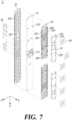
- FIG. 7 is an exploded perspective view of the antenna device according to another embodiment of the present disclosure.
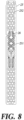
- FIG. 8 is a bottom view of the antenna device according to another embodiment of the present disclosure.
- the antenna device 2 includes all or some of a plate 21, a first dielectric plate 22, a first feed line 23, a plurality of radiation elements 14, a second dielectric plate 25, and a second feed line 26.
- the first dielectric plate 22 may include all or some of a first groove 221, a second groove 222, a first support unit 223, a first connection unit 224, and a second connection unit 225.
- the first feed line 23 may include a main line region 231, a connection line region 232, and an input/output region 233.
- the first dielectric plate 22 may be coupled to an upper surface of the antenna device 2, and the second dielectric plate 22 may be coupled to a lower surface.
- the first dielectric plate 22 and the second dielectric plate 25 may be respectively formed on the upper and lower surfaces of the plate 21 through double injection.
- the plate 21 may include a variable circuit board 211 and a coupling portion 212.
- the variable circuit board 211 is a type of printed circuit board, and a variable circuit having at least one power disconnection point that can change the phase of the frequency using the feed lines 23 and 26 may be printed in a pattern on an upper surface of the variable circuit board 211.
- the variable circuit board 211 may be electrically connected to the first feed line 23 and/or the second feed line 26.
- the coupling portion 212 may couple the plate 21, the first dielectric plate 22, and the second dielectric plate 25.
- the coupling portion 212 may each have a pair of bolt/nut structure, but is not limited thereto and may have any structure capable of combining the plate 21, the first dielectric plate 22, and the second dielectric plate 25.
- the second dielectric plate 25 may include all or part of a third groove 251 and a fourth groove 252.
- the third groove 251 and the fourth groove 252 may be formed integrally with the second dielectric plate 25.
- the second dielectric plate 25 may be made of a dielectric material, for example, a plastic material.
- the third groove 251 may be formed to penetrate upper and lower surfaces of the second dielectric plate 25.
- the third groove 251 may extend longitudinally along the first direction.
- the first direction is a direction parallel to the Y-axis of FIG. 7 .
- the third groove 251 may be formed to correspond to the shape of the second feed line 26 so that the second feed line 26 can float in the third groove 251.
- the second feed line 26 may be configured to float in the third groove 251.
- the second feed line 26 may float at a predetermined distance from the side wall of the third groove 251.
- the second feed line 26 may float at a predetermined distance from the plate 21 coupled to the lower surface of the second dielectric plate 25.
- the space between the second feed line 26 and the side wall of the third groove 251 and/or the plate 21 may be filled with air. That is, the second feed line 26 may have an air-strip line structure like the first feed line 23.
- the fourth groove 252 may be formed in at least a portion of the second dielectric plate 25 where the third groove 251 is not formed.
- the fourth groove 252 may be formed to penetrate the upper and lower surfaces of the second dielectric plate 25.
- the fourth groove 252 may be formed regularly with a predetermined pattern.
- the fourth groove 252 may be formed in a honeycomb-shaped pattern.
- the present disclosure is not limited to the above, and the fourth groove 252 may be formed irregularly.
- the second feed line 26 may not have a bent shape.
- the second feed lines 26 may be paired and be arranged symmetrically to each other.
- the second feed line 26 may extend longitudinally along the first direction.
- the second feed line 26 may be used when length compensation using the delay line of the first feed line 23 is not possible.
- a parallel feed design to be described later can be applied.
- one end of the second feed line 26 may be connected to the input/output region 233 of the first feed line 23, and the other end may be connected to the RF circuit.
- the other end of the second feed line 26 may be connected to the RF circuit provided with a filter, a power amplifier, a power supply unit, and the like.
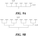
- FIGS. 9A and 9B are diagrams showing the connection relationship of the feed lines according to one embodiment of the present disclosure.
- FIG. 9A is a diagram schematically showing a circuit diagram when supplying power to the plurality of radiation elements 14 and 24 in series.
- the gap between two adjacent radiation elements 14, 24 may be 1 lambda.
- side lobes may occur due to a large phase difference between the plurality of radiation elements 14 and 24 on the phase slope, making it difficult to obtain a wide bandwidth of the antenna devices 1 and 2.
- FIG. 9B is a diagram schematically showing a circuit diagram when supplying power to the plurality of radiation elements 14 and 24 in parallel.
- the two adjacent radiation elements 14 and 24 may be identical in terms of phase.
- the phase difference in the phase slope is gentle, so the antenna devices 1 and 2 can obtain a wide bandwidth.
- Series feeding and parallel feeding can be applied to the antenna device 1 and the antenna device 2 according to one embodiment and another embodiment of the present disclosure, respectively.
- the present disclosure is not limited to this, and series feeding may be applied to the antenna device 2 according to another embodiment, or parallel feeding may be applied to the antenna device 1 according to one embodiment.
- series feeding and parallel feeding may be combined and applied to the antenna device 1 and the antenna device 2 according to one embodiment and another embodiment of the present disclosure.
Landscapes
- Engineering & Computer Science (AREA)
- Manufacturing & Machinery (AREA)
- Physics & Mathematics (AREA)
- Electromagnetism (AREA)
- Variable-Direction Aerials And Aerial Arrays (AREA)
- Waveguide Aerials (AREA)
Abstract
Description
- The present disclosure relates to an air-strip line and an antenna device including the air-strip line.
- The content described in this section merely provides background information related to one embodiment of the present disclosure and does not constitute prior art.
- The antenna device may include a plate, a radiation element, and a feed line that supplies power to the radiation element. The size of the radiation element may vary depending on the frequency of use. For example, as the operating frequency increases, the size of the radiation element decreases.
- Multiple feed lines may be printed in a pattern on a substrate. However, since the substrate is made of a PCB material (for example, FR4 material) with a predetermined dielectric constant, the insertion loss due to the multiple pattern-printed feed lines increases, which deteriorates the performance of the antenna device.
- Loss due to feed lines can be divided into conductor loss in the conductor through which the signal flows and dielectric loss due to the dielectric surrounding the conductor. The loss directly reduces the gain of the antenna device. In order to improve the gain of the antenna device, it is necessary to improve the loss, and since changing or deforming the medium is relatively advantageous, improving the dielectric loss is effective.
- A representative example of the feed line used to improve dielectric loss is an air-strip line structure. The air-strip line structure refers to a feed line structure in which the dielectric portion is implemented as air.
- In a feed line of the air-strip line structure, the dielectric loss is close to 0 because the conductor is surrounded by air. Therefore, when using a feed line of the air-strip line structure, the dielectric loss can be reduced, which increases the gain of the antenna device.
- In a conventional air-strip line structure, the impedance can be varied by adjusting the width of the feed line. However, in the conventional air-strip line structure, the width of the feed line is wider for the same impedance compared to the PCB type, so adjusting the width of the feed line to vary the impedance has limitations in the design of the antenna device.
- In addition, when the width of the feed line is adjusted, a height difference may occur between the feed lines during processing, and the characteristics of the antenna device may be deteriorated due to the height difference.
- According to one embodiment of the present disclosure, the present disclosure provides an antenna device capable of adjusting the distance between a feed line and a dielectric plate and the thickness of the dielectric plate.
- According to one embodiment of the present disclosure, the present disclosure provides an antenna device capable of configuring a circuit by changing only the structure of the dielectric while reducing the change in the width of the feed line.
- The objects to be achieved by the present disclosure are not limited to the objects mentioned above, and other objects not mentioned will be clearly understood by a person of ordinary skill in the art from the description below.
- According to one embodiment of the present disclosure, an antenna device comprising:
a plate; a first dielectric plate coupled to one surface of the plate; a plurality of radiation elements arranged along a first direction on the first dielectric plate; and a plurality of first feed lines configured to supply power to the plurality of radiation elements and having an air-strip line structure, wherein the first dielectric plate includes a first groove penetrating upper and lower surfaces of the first dielectric plate and configured to allow the first feed line to float therein, and the first feed line is configured to float in the first groove. - According to one embodiment of the present disclosure, a feed line of an air-strip line structure which supplies power to a radiation element of an antenna device, the feed line comprising: a dielectric plate; a groove formed to penetrate through upper and lower surfaces of the dielectric plate; and a line unit configured to float at a predetermined distance from a side wall of the groove.
- According to one embodiment, the antenna device can vary the impedance by adjusting the distance between the feed line and the dielectric plate and the thickness of the dielectric plate.
- According to one embodiment, the antenna device can minimize the height difference that occurs when manufacturing the feed line by reducing the change in the width of the feed line.
-
-
FIG. 1 is a combined perspective view of an antenna device according to one embodiment of the present disclosure. -
FIG.2 is an exploded perspective view of the antenna device according to one embodiment of the present disclosure. -
FIG.3 is an enlarged top view of part B ofFIG. 1 . -
FIG. 4 is a cross-sectional view taken along line AA' ofFIG. 1 and a graph showing the change in impedance according to the distance between a feed line and a dielectric plate. -
FIG. 5 is a graph showing a dielectric portion added to the bottom of the feed line and a change in impedance depending on the thickness of the dielectric portion according to one embodiment of the present disclosure. -
FIG. 6 is a combined perspective view of an antenna device according to another embodiment of the present disclosure. -
FIG. 7 is an exploded perspective view of the antenna device according to another embodiment of the present disclosure. -
FIG. 8 is a bottom view of the antenna device according to another embodiment of the present disclosure. -
FIGS. 9A and 9B are diagrams showing the connection relationship of feed lines according to one embodiment of the present disclosure. - Hereinafter, some exemplary embodiments of the present disclosure will be described in detail with reference to the accompanying drawings. In the following description, like reference numerals preferably designate like elements, although the elements are shown in different drawings. Further, in the following description of some embodiments, a detailed description of known functions and configurations incorporated therein will be omitted for the purpose of clarity and for brevity.
- Additionally, various terms such as first, second, A, B, i), ii), (a), (b), a), b), etc., are used solely to differentiate one component from the other but not to imply or suggest the substances, order, or sequence of the components. Throughout this specification, when a part 'includes' or 'comprises' a component, the part is meant to further include other components, not to exclude thereof unless specifically stated to the contrary.
- In the present specification, "upper surface" or "upper portion" refers to the direction in which
radiation elements antenna devices plates antenna devices -
FIG. 1 is a combined perspective view of an antenna device according to one embodiment of the present disclosure. -
FIG.2 is an exploded perspective view of the antenna device according to one embodiment of the present disclosure. - Referring to
FIGS. 1 and2 , anantenna device 1 may include all or some of aplate 11, afirst dielectric plate 12, afirst feed line 13, and a plurality ofradiation elements 14. - The
first dielectric plate 12 may be coupled to an upper surface of theplate 11. Theplate 11 may be made of a metallic material and may provide a ground plane for theradiation elements 14 of theantenna device 1. - The
plate 11 may include a plurality ofholes 111. The plurality ofholes 111 may be formed to penetrate theplate 11. The plurality ofholes 111 may include a plurality of first holes and a plurality of second holes. Protrusions (not shown) of thefirst dielectric plate 12 are inserted into the plurality of first holes, so that theplate 11 and thefirst dielectric plate 12 can be coupled. RF filters, connectors, ports, etc. may be coupled in the plurality of second holes to be connected to theantenna device 1. - The
first dielectric plate 12 may include all or some of afirst groove 121, asecond groove 122, afirst support unit 123, afirst connection unit 124, asecond connection unit 125, and a protrusion (not shown). - The
first dielectric plate 12 may be formed on the upper surface of theplate 11 through injection. Thus, all or some of the components of thefirst dielectric plate 12, thefirst groove 121, thesecond groove 122, thefirst support unit 123, thefirst connection unit 124, thesecond connection unit 125, and the protrusions may be formed integrally. In this case, thefirst dielectric plate 12 may be made of a dielectric, e.g., plastic material. - The
first groove 121 may be formed to penetrate the upper and lower surfaces of thefirst dielectric plate 12. Thefirst groove 121 may extend longitudinally along a first direction. In this case, the first direction is a direction parallel to the Y-axis ofFIG. 1 . Thefirst groove 121 may be formed to correspond to the shape of thefirst feed line 13, which will be described later, so that thefirst feed line 13 can float in thefirst groove 121. - The
first feed line 13 may be configured to float in thefirst groove 121. For example, thefirst feed line 13 may float at a predetermined distance from the side wall of thefirst groove 121. In addition, thefirst feed line 13 may float at a predetermined distance from theplate 11 coupled to the lower surface of thefirst dielectric plate 12. - The space between the
first feed line 13 and the side wall of thefirst groove 121 and/or theplate 11 may be filled with air. That is, thefirst feed line 13 may have an air-strip line structure. The air-strip line structure refers to a structure in which the dielectric portion is implemented as air in a general stripline structure. - In the
feed line 13 of the air-strip line structure, the dielectric loss is close to '0' because the conductor is surrounded by air. Therefore, the gain of theantenna device 1 can be increased by reducing the dielectric loss. - The
first support unit 123 may be formed in thefirst groove 121. Thefirst support unit 123 is formed at the bottom of thefirst groove 121 and may connect opposing side walls of thefirst groove 121. Thefirst support unit 123 may be connected to thefirst groove 121 and formed integrally with thefirst dielectric plate 12, but a thickness of thefirst support unit 123 may be thinner than a thickness of thefirst groove 121. Thefirst support unit 123 may be formed in thefirst groove 121 at predetermined intervals along the first direction. - The
first feed line 13 may be coupled to upper surfaces of a plurality offirst support units 123 formed at predetermined intervals. As thefirst feed line 13 is coupled to the upper surfaces of thefirst support unit 123, thefirst feed line 13 may float at a predetermined distance from the side wall of thefirst groove 121 and/or theplate 11. That is, by using thefirst support unit 123, an air-strip line structure can be formed using only a minimum amount of dielectric. - The
second groove 122 may be formed in at least a portion of thefirst dielectric plate 12 where thefirst groove 121 is not formed. Thesecond groove 122 may be formed to penetrate the upper and lower surfaces of thefirst dielectric plate 12. Thesecond groove 122 may be formed regularly with a predetermined pattern. For example, thesecond groove 122 may be formed in a honeycomb-shaped pattern. However, the present disclosure is not limited to the above, and thesecond groove 122 may be formed irregularly. By forming a plurality ofsecond grooves 122 in thefirst dielectric plate 12, the weight of thefirst dielectric plate 12 can be lightened and the manufacturing cost of theantenna device 1 can be reduced. - The
first connection unit 124 may be formed to protrude from the upper surface of thefirst dielectric plate 12. Thefirst connection unit 124 may connect thefirst dielectric plate 12 and theradiation element 14. Fourfirst connection units 124 may be formed at predetermined intervals to connect thefirst dielectric plate 12 and theradiation element 14. For example, the fourfirst connection units 124 may be arranged to form a square shape. However, the present disclosure is not limited to the above, and the number and arrangement of thefirst connection units 124 may be designed in various ways as needed. - The
second connection unit 125 may be formed to protrude from the upper surface of thefirst dielectric plate 12 . Thesecond connection unit 125 may connect thefirst dielectric plate 12 and thefirst feed line 13. Thesecond connection unit 125 may be formed below theradiation element 14 so that thefirst feed line 13 can feed theradiation element 14. That is, the height of thesecond connection unit 125 may be lower than the height of thefirst connection unit 124. In order to connect a pair offirst feed lines 13, thesecond connection units 125 may be formed as a pair. However, the present disclosure is not limited to the above, and the number and arrangement of thesecond connection units 125 may be designed in various ways as needed. - The protrusion may be formed on the lower surface of the
first dielectric plate 12. The protrusion is formed to protrude from the lower surface of thefirst dielectric plate 12 and can be inserted into thehole 111 of theplate 11. Thefirst dielectric plate 12 and theplate 11 may be coupled by inserting the protrusions into theholes 111. A plurality of protrusions may be formed corresponding to the positions of theholes 111 of theplate 11. The plurality of protrusions may be formed integrally with thefirst dielectric plate 12. - A plurality of
radiation elements 14 may be arranged in a row along the first direction. In this case, the plurality ofradiation elements 14 may form one antenna column. Here, the first direction is a direction parallel to the Y-axis ofFIG. 1 . - When the intermediate frequency of the operating frequency band is lambda, within one antenna column, if the gap between one
radiation element 14 and its neighboringradiation element 14 is equal to or more than 1 lambda, undesirable grating lobes may occur in the radiation pattern. - Therefore, it is preferable that the gap between one
radiation element 14 and its neighboringradiation element 14 in the first direction is less than 1 lambda. However, the present disclosure is not limited to the above, and the gap in the first direction between the tworadiation elements 14 may have a value outside the above-described range. - The
antenna device 1 may include a plurality of antenna columns. A plurality of antenna columns may be arranged on theplate 11 along a second direction perpendicular to the first direction. In this case, the second direction is a direction parallel to the X-axis ofFIG. 1 . - The plurality of
radiation elements 14 may be configured to implement dual polarization. Thefirst feed line 13 may be configured as a pair so that theradiation element 14 implements dual polarization. The pair offirst feed lines 13 may be arranged symmetrically. For example, two types of polarized signals of +45 degrees and -45 degrees may be radiated from oneradiation element 14. However, the present disclosure is not limited to the above, and theradiation element 14 may be configured to implement single polarization or quadruple polarization. - The
first feed line 13 may be configured to supply power to a plurality ofradiation elements 14. That is, the plurality ofradiation elements 14 can transmit and receive signals or receive power using thefirst feed line 13. - The
first feed line 13 may include amain line region 131, aconnection line region 132, and an input/output region 133. Themain line region 131 may extend longitudinally along the first direction. Theconnection line region 132 may have one end connected to thesecond connection unit 125 and the other end connected to themain line region 131. Theconnection line region 132 may be formed by bending themain line region 131 at a predetermined angle. For example, theconnection line region 132 may be formed by bending themain line region 131 into an 'L' shape. However, the present disclosure is not limited to the above, and theconnection line region 132 may be formed obliquely. - The
connection line region 132 may be branched from themain line region 131, and eachconnection line region 132 may be connected to the correspondingradiation element 14. Theconnection line region 132 may be directly connected to theradiation element 14, or may be connected by a coupling method. - The input/
output region 133 may be branched from themain line region 131 and may connect an RF circuit to themain line region 131. One end of the input/output region 133 may be connected to themain line region 131, and the other end of the input/output region 133 may be connected to the RF circuit provided with a filter, a power amplifier, a power supply unit, and the like. - The RF circuit may be provided inside the
antenna device 1, but may also be provided in an external device outside theantenna device 1, for example, a remote radio head (RRH). When the RF circuit is provided in an external device such as the RRH, theantenna device 1 and the external device with the RF circuit may be connected using an RF cable, a connector, or the like. - The input/
output region 133 may transmit signals transmitted from the RF circuit to the plurality ofradiation elements 14 or transmit signals received them from the plurality ofradiation elements 14 to the RF circuit, using themain line region 131 and theconnection line region 132. In addition, the input/output region 133 may supply power to the plurality ofradiation elements 14 using themain line region 131 and theconnection line region 132. - In order to minimize phase difference or power loss that may occur due to an increase in the length of the
first feed line 13, the input/output region 133 may be disposed near the middle portion of themain line region 131. - Meanwhile, in the air-strip line structure, the dielectric portion is implemented as air, so the length of the
first feed line 13 for inputting the same phase to the plurality ofradiation elements 14 may be relatively long. - For example, when the intermediate frequency of the operating frequency band is lambda, the length of the
first feed line 13 required to input signals of the same phase to the first radiation element and the second radiation element adjacent to the first radiation element may be 1 lambda. That is, the length of thefirst feed line 13 from the first connection line region and the second connection line region adjacent to the first connection line region may be 1 lambda. - As described above, in order to minimize the occurrence of grating lobes, the gap in the first direction between two
adjacent radiation elements 14 is preferably less than 1 lambda. In this case, the length of the first feed line connecting the twoadjacent radiation elements 14 may be longer than the gap between the twoadjacent radiation elements 14, which may be a problem. - To solve this problem, the
main line region 131 may include a delay line. The delay line may be formed in at least a portion of themain line region 131. The delay line may be an area formed by bending a portion of themain line region 131, and may partially compensate for the length of thefirst feed line 13, which has become longer. - In a pair of
first feed lines 13, the delay line may have a concave shape or a convex shape toward the otherfirst feed line 13. For example, the delay line may have a 'C' shape, but the present disclosure is not limited thereto. - With the
main line region 131 including the delay line, the distance between the twoadjacent radiation elements 14 in the first direction can be prevented from inevitably increasing. Accordingly, theantenna device 1 can be compact, and the occurrence of undesirable grating lobes can be minimized. -
FIG. 3 is an enlarged top view of part B ofFIG. 1 . - Referring to
FIG. 3 , thefirst feed line 13 of theantenna device 1 of the present disclosure may be configured to float in thefirst groove 121. Thefirst feed line 13 may float at a predetermined distance from the side wall of thefirst groove 121. Thefirst support unit 123 may support thefirst feed line 13 so that thefirst feed line 13 can float at the predetermined distance from the side wall of thefirst groove 121. - The
antenna device 1 of the present disclosure may vary the impedance by adjusting the gap between thefirst feed line 13 and the side wall of thefirst groove 121 while maintaining the width of thefirst feed line 13 constant. Thefirst feed line 13 may have a uniform width. Therefore, unlike a conventional air-strip line structure in which the width of the feed line is adjusted to vary the impedance, there is an effect of minimizing a height difference that occurs when manufacturing thefirst feed line 13. Accordingly, theantenna device 1 of the present disclosure can also minimize burr problems that occur when manufacturing the air-strip line structure. -
FIG. 4 is a cross-sectional view taken along line AA' ofFIG. 1 and a graph showing the change in impedance according to the distance between the feed line and the dielectric plate. - Referring to
FIG. 4 , theantenna device 1 of the present disclosure is capable of adjusting the distance between thefirst feed line 13 and the side wall of thefirst groove 121. Since the width of thefirst feed line 13 is constant, the width of thefirst groove 121 needs to be adjusted to adjust the distance between thefirst feed line 13 and the side wall of thefirst groove 121. For example, the distance between thefirst feed line 13 and the side wall of thefirst groove 121 can be increased or decreased by adjusting the thickness of the side wall of thefirst groove 121. The width of thefirst groove 121 can be designed using a preset value during the manufacturing process of thefirst dielectric plate 12. - Referring to the graph of
FIG. 4 , it can be seen that the impedance increases as the distance (clearance) between thefirst feed line 13 and the side wall of thefirst groove 121 increases. That is, theantenna device 1 of the present disclosure can adjust the dielectric constant and impedance by adjusting the distance between thefirst feed line 13 and the side wall of thefirst groove 121. -
FIG. 5 is a graph showing a dielectric portion added to the bottom of the feed line and a change in impedance change depending on the thickness of the dielectric portion according to one embodiment of the present disclosure. - Referring to
FIG. 5 , thefirst dielectric plate 12 of theantenna device 1 of the present disclosure may further include adielectric portion 126. - The
dielectric portion 126 may be formed in thefirst groove 121. Thedielectric portion 126 may be formed at the bottom of thefirst groove 121 and may connect opposing side walls of thefirst groove 121. Thedielectric portion 126 may be integrally formed with thefirst dielectric plate 12 to be connected to thefirst groove 121, and the thickness of thedielectric portion 126 may be thinner than the thickness of thefirst groove 121. - The
dielectric portion 126 may be formed in at least a portion of thefirst groove 121 where thefirst support unit 123 is not formed. Thedielectric portion 126 may be formed continuously or may be formed regularly at predetermined intervals. Thedielectric portion 126 may be formed at the bottom of thefirst dielectric plate 12 to be spaced apart by predetermined distance from thefirst feed line 13. The shape and thickness of thedielectric portion 126 may be designed in various ways as needed. - Referring to the graph of
FIG. 5 , it can be seen that the impedance varies depending on the distance between thefirst feed line 13 and thedielectric portion 126. It can be seen that as the thickness t of thedielectric portion 126 increases, that is, as the distance between thefirst feed line 13 and thedielectric portion 126 decreases, the impedance increases. That is, theantenna device 1 of the present disclosure can adjust the dielectric constant and impedance by adjusting the distance between thefirst feed line 13 and thedielectric portion 126. -
FIG. 6 is a combined perspective view of an antenna device according to another embodiment of the present disclosure. -
FIG. 7 is an exploded perspective view of the antenna device according to another embodiment of the present disclosure. -
FIG. 8 is a bottom view of the antenna device according to another embodiment of the present disclosure. - Referring to
FIGS. 6 to 8 , theantenna device 2 according to another embodiment of the present disclosure includes all or some of aplate 21, afirst dielectric plate 22, afirst feed line 23, a plurality ofradiation elements 14, asecond dielectric plate 25, and asecond feed line 26. - The
first dielectric plate 22 may include all or some of afirst groove 221, asecond groove 222, afirst support unit 223, afirst connection unit 224, and asecond connection unit 225. Thefirst feed line 23 may include amain line region 231, aconnection line region 232, and an input/output region 233. - In the descriptions of the
plate 21, thefirst dielectric plate 22, thefirst feed line 23, the plurality ofradiation elements 14, and each configuration of theantenna device 2 according to another embodiment of the present disclosure, descriptions of parts overlapping with theantenna device 1 according to one embodiment of the disclosure are replaced with the contents described above. In addition, for convenience of explanation, only one antenna column is disposed inFIGS. 6 to 8 , but the present disclosure is not limited to this and a plurality of antenna columns may be disposed. - The
first dielectric plate 22 may be coupled to an upper surface of theantenna device 2, and thesecond dielectric plate 22 may be coupled to a lower surface. Thefirst dielectric plate 22 and thesecond dielectric plate 25 may be respectively formed on the upper and lower surfaces of theplate 21 through double injection. - The
plate 21 may include avariable circuit board 211 and acoupling portion 212. Thevariable circuit board 211 is a type of printed circuit board, and a variable circuit having at least one power disconnection point that can change the phase of the frequency using thefeed lines variable circuit board 211. Thevariable circuit board 211 may be electrically connected to thefirst feed line 23 and/or thesecond feed line 26. Thecoupling portion 212 may couple theplate 21, thefirst dielectric plate 22, and thesecond dielectric plate 25. Thecoupling portion 212 may each have a pair of bolt/nut structure, but is not limited thereto and may have any structure capable of combining theplate 21, thefirst dielectric plate 22, and thesecond dielectric plate 25. - The
second dielectric plate 25 may include all or part of athird groove 251 and afourth groove 252. Thethird groove 251 and thefourth groove 252 may be formed integrally with thesecond dielectric plate 25. In this case, thesecond dielectric plate 25 may be made of a dielectric material, for example, a plastic material. - The
third groove 251 may be formed to penetrate upper and lower surfaces of thesecond dielectric plate 25. Thethird groove 251 may extend longitudinally along the first direction. In this case, the first direction is a direction parallel to the Y-axis ofFIG. 7 . Thethird groove 251 may be formed to correspond to the shape of thesecond feed line 26 so that thesecond feed line 26 can float in thethird groove 251. - The
second feed line 26 may be configured to float in thethird groove 251. For example, thesecond feed line 26 may float at a predetermined distance from the side wall of thethird groove 251. In addition, thesecond feed line 26 may float at a predetermined distance from theplate 21 coupled to the lower surface of thesecond dielectric plate 25. - The space between the
second feed line 26 and the side wall of thethird groove 251 and/or theplate 21 may be filled with air. That is, thesecond feed line 26 may have an air-strip line structure like thefirst feed line 23. - The
fourth groove 252 may be formed in at least a portion of thesecond dielectric plate 25 where thethird groove 251 is not formed. Thefourth groove 252 may be formed to penetrate the upper and lower surfaces of thesecond dielectric plate 25. Thefourth groove 252 may be formed regularly with a predetermined pattern. For example, thefourth groove 252 may be formed in a honeycomb-shaped pattern. However, the present disclosure is not limited to the above, and thefourth groove 252 may be formed irregularly. By forming a plurality offourth grooves 252 in thesecond dielectric plate 25, the weight of thesecond dielectric plate 25 can be lightened and the manufacturing cost of theantenna device 2 can be reduced. - Unlike the
first feed line 23, thesecond feed line 26 may not have a bent shape. Thesecond feed lines 26 may be paired and be arranged symmetrically to each other. Thesecond feed line 26 may extend longitudinally along the first direction. Thesecond feed line 26 may be used when length compensation using the delay line of thefirst feed line 23 is not possible. By using thesecond feed line 26, a parallel feed design to be described later can be applied. For example, one end of thesecond feed line 26 may be connected to the input/output region 233 of thefirst feed line 23, and the other end may be connected to the RF circuit. The other end of thesecond feed line 26 may be connected to the RF circuit provided with a filter, a power amplifier, a power supply unit, and the like. -
FIGS. 9A and 9B are diagrams showing the connection relationship of the feed lines according to one embodiment of the present disclosure. -
FIG. 9A is a diagram schematically showing a circuit diagram when supplying power to the plurality ofradiation elements adjacent radiation elements radiation elements antenna devices -
FIG. 9B is a diagram schematically showing a circuit diagram when supplying power to the plurality ofradiation elements adjacent radiation elements antenna devices - Series feeding and parallel feeding can be applied to the
antenna device 1 and theantenna device 2 according to one embodiment and another embodiment of the present disclosure, respectively. However, the present disclosure is not limited to this, and series feeding may be applied to theantenna device 2 according to another embodiment, or parallel feeding may be applied to theantenna device 1 according to one embodiment. In addition, series feeding and parallel feeding may be combined and applied to theantenna device 1 and theantenna device 2 according to one embodiment and another embodiment of the present disclosure. - Although exemplary embodiments of the present disclosure have been described for illustrative purposes, those skilled in the art will appreciate that various modifications, additions, and substitutions are possible, without departing from the idea and scope of the claimed invention. Therefore, exemplary embodiments of the present disclosure have been described for the sake of brevity and clarity. The scope of the technical idea of the present embodiments is not limited by the illustrations. Accordingly, one of ordinary skill would understand the scope of the claimed invention is not to be limited by the above explicitly described embodiments but by the claims and equivalents thereof.
-
- 1: antenna device 11: plate
- 111: hole 12: first dielectric plate
- 121: first groove 122: second groove
- 123: first support unit 124: first connection unit
- 125: second connection unit 13: first feed line
- 131: main line region 132: connection line region
- 133: input/output region 14: radiation element
- 2: antenna device 21: plate
- 211: variable circuit board 22: first dielectric plate
- 221: first groove 222: second groove
- 223: first support unit 224: first connection unit
- 225: second connection unit 23: first feed line
- 231: main line region 232: connection line region
- 233: input/output region 24: radiation element
- 25: second dielectric plate 251: third groove
- The present application claims priority to
Korean Patent Application No. 10-2022-0002899 filed on January 7, 2022 Korean Patent Application No. 10-2022-0041049 filed on April 1, 2022
Claims (15)
- An antenna device comprising:a plate;a first dielectric plate coupled to one surface of the plate;a plurality of radiation elements arranged along a first direction on the first dielectric plate; anda plurality of first feed lines configured to supply power to the plurality of radiation elements and having an air-strip line structure,wherein the first dielectric plate includes a first groove penetrating upper and lower surfaces of the first dielectric plate and configured to allow the first feed line to float therein, and the first feed line is configured to float in the first groove.
- The antenna device of claim 1, wherein the first feed line floats at a predetermined distance from a side wall of the first groove.
- The antenna device of claim 1, wherein the first dielectric plate further includes a dielectric portion between the first feed line and the plate.
- The antenna device of claim 1, wherein the first groove has a shape corresponding to a shape of the first feed line.
- The antenna device of claim 1, wherein the first dielectric plate further includes one or more first support units formed in at least a portion of the first groove to support the first feed line.
- The antenna device of claim 5, wherein the first support units are arranged at predetermined intervals and are formed integrally with the first dielectric plate.
- The antenna device of claim 1, wherein the first dielectric plate further includes a first connection unit connecting the first dielectric plate to the radiation element and a second connection unit connecting the first dielectric plate to the first feed line, and
the first connection unit and the second connection unit are formed integrally with the first dielectric plate. - The antenna device of claim 1, further comprising a second dielectric plate coupled to the other surface of the plate and a plurality of second feed lines configured to transmit signals to the first feed line.
- The antenna device of claim 8, wherein the second dielectric plate includes a third groove configured to penetrate upper and lower surfaces of the second dielectric plate in which the second feed line is disposed, and the second feed line is configured to float in the third groove.
- The antenna device of claim 8, wherein the first dielectric plate and the second dielectric plate are injection molded.
- The antenna device of claim 1, wherein the first feed line has a uniform width.
- A feed line of an air-strip line structure which supplies power to a radiation element of an antenna device, the feed line comprising:a dielectric plate;a groove formed to penetrate through upper and lower surfaces of the dielectric plate; anda line unit configured to float at a predetermined distance from a side wall of the groove.
- The feed line of claim 12, further comprising one or more support units formed in at least a portion of the groove to support the line unit.
- The feed line of claim 13, wherein the groove is formed to extend in a first direction, and
the support units are arranged at predetermined intervals along the first direction. - The feed line of claim 12, wherein the line unit has a uniform width.
Applications Claiming Priority (3)
| Application Number | Priority Date | Filing Date | Title |
|---|---|---|---|
| KR20220002899 | 2022-01-07 | ||
| KR1020220041049A KR20230107464A (en) | 2022-01-07 | 2022-04-01 | Air-Strip Line And Antenna Device Including Air-Strip Line |
| PCT/KR2023/000349 WO2023132712A1 (en) | 2022-01-07 | 2023-01-09 | Air-strip line and antenna device comprising air-strip line |
Publications (2)
| Publication Number | Publication Date |
|---|---|
| EP4462599A1 true EP4462599A1 (en) | 2024-11-13 |
| EP4462599A4 EP4462599A4 (en) | 2025-12-10 |
Family
ID=87074009
Family Applications (1)
| Application Number | Title | Priority Date | Filing Date |
|---|---|---|---|
| EP23737460.8A Pending EP4462599A4 (en) | 2022-01-07 | 2023-01-09 | Air current line and antenna device with air current line |
Country Status (4)
| Country | Link |
|---|---|
| US (1) | US20240364021A1 (en) |
| EP (1) | EP4462599A4 (en) |
| JP (1) | JP7755752B2 (en) |
| WO (1) | WO2023132712A1 (en) |
Family Cites Families (21)
| Publication number | Priority date | Publication date | Assignee | Title |
|---|---|---|---|---|
| US5086304A (en) * | 1986-08-13 | 1992-02-04 | Integrated Visual, Inc. | Flat phased array antenna |
| JPS6369301A (en) * | 1986-09-11 | 1988-03-29 | Yuniden Kk | Shared planar antenna for polarized wave |
| JPH027703A (en) * | 1988-06-27 | 1990-01-11 | Sharp Corp | planar antenna |
| US5608263A (en) * | 1994-09-06 | 1997-03-04 | The Regents Of The University Of Michigan | Micromachined self packaged circuits for high-frequency applications |
| JPH11186837A (en) * | 1997-12-24 | 1999-07-09 | Mitsubishi Electric Corp | Array antenna device |
| US6888427B2 (en) | 2003-01-13 | 2005-05-03 | Xandex, Inc. | Flex-circuit-based high speed transmission line |
| US7288723B2 (en) * | 2003-04-02 | 2007-10-30 | Sun Microsystems, Inc. | Circuit board including isolated signal transmission channels |
| JP2013005296A (en) * | 2011-06-17 | 2013-01-07 | Hitachi Chem Co Ltd | Line interlayer connector, planar array antenna having line interlayer connector and planar array antenna module |
| US9178257B2 (en) * | 2012-12-06 | 2015-11-03 | Anaren, Inc. | First and second microstrip networks stacked in an inverted arrangement to each other using an integrated support and shielding structure |
| JP5675934B1 (en) * | 2013-11-06 | 2015-02-25 | 有限会社Nazca | Antenna device |
| KR102033311B1 (en) * | 2013-11-22 | 2019-10-17 | 현대모비스 주식회사 | Microstripline-fed slot array antenna and manufacturing method thereof |
| KR101663139B1 (en) * | 2015-02-25 | 2016-10-10 | 블루웨이브텔(주) | High-efficient rf transmission line structure and its application components |
| CN206364178U (en) * | 2016-12-09 | 2017-07-28 | 安徽四创电子股份有限公司 | A kind of micro-strip array antenna |
| CN106602281A (en) * | 2016-12-20 | 2017-04-26 | 北京佰才邦技术有限公司 | Feed network and antenna array |
| KR102410799B1 (en) * | 2017-11-28 | 2022-06-21 | 삼성전자주식회사 | Antenna system for transmitting and receiving mm-wave signal |
| CN210576472U (en) * | 2019-05-24 | 2020-05-19 | 中兴通讯股份有限公司 | An antenna vibrator, antenna unit, antenna and communication equipment |
| US11276933B2 (en) * | 2019-11-06 | 2022-03-15 | The Boeing Company | High-gain antenna with cavity between feed line and ground plane |
| CN213093372U (en) * | 2020-09-10 | 2021-04-30 | 苏州硕贝德创新技术研究有限公司 | Compact microstrip array antenna and radiation unit |
| CN214227138U (en) * | 2021-01-29 | 2021-09-17 | 大富科技(安徽)股份有限公司 | Feed unit, metal conduction band feed network and antenna structure |
| CN112993561B (en) * | 2021-04-23 | 2021-07-30 | 四川斯艾普电子科技有限公司 | Antenna low-profile adapter plate, adapter method and dual-band common-caliber antenna |
| CN214477926U (en) * | 2021-04-30 | 2021-10-22 | 成都卫信科技有限公司 | Array antenna and waveguide conversion device |
-
2023
- 2023-01-09 EP EP23737460.8A patent/EP4462599A4/en active Pending
- 2023-01-09 WO PCT/KR2023/000349 patent/WO2023132712A1/en not_active Ceased
- 2023-01-09 JP JP2024539308A patent/JP7755752B2/en active Active
-
2024
- 2024-07-05 US US18/764,416 patent/US20240364021A1/en active Pending
Also Published As
| Publication number | Publication date |
|---|---|
| US20240364021A1 (en) | 2024-10-31 |
| JP2024545909A (en) | 2024-12-13 |
| JP7755752B2 (en) | 2025-10-16 |
| EP4462599A4 (en) | 2025-12-10 |
| WO2023132712A1 (en) | 2023-07-13 |
Similar Documents
| Publication | Publication Date | Title |
|---|---|---|
| US11626652B2 (en) | Ridge gap waveguide and multilayer antenna array including the same | |
| US6864851B2 (en) | Low profile wideband antenna array | |
| EP3621146B1 (en) | High frequency filter and phased array antenna comprising such a high frequency filter | |
| CN109314314B (en) | Array antenna | |
| EP2214259B1 (en) | Method and apparatus for forming millimeter wave phased array antenna | |
| CA1080351A (en) | Radio frequency antenna arrays of radiating slot apertures | |
| CN1547788B (en) | Adjustable antenna feed network with integrated phase shifter | |
| JP4888143B2 (en) | T-branch waveguide and array antenna | |
| KR20200011500A (en) | Tripolar Current Loop Radiating Element with Integrated Circular Polarization Feed | |
| KR100897864B1 (en) | Power Divider with Coupling | |
| JPH10308627A (en) | Formed beam array antenna | |
| KR20210005285A (en) | Waveguide slot antenna | |
| US11394114B2 (en) | Dual-polarized substrate-integrated 360° beam steering antenna | |
| WO2025036025A1 (en) | Circularly polarized antenna, array antenna, and communication device | |
| CN116487841B (en) | Gap waveguide liquid crystal phase shifter | |
| CN113300124B (en) | Right-hand circularly polarized array antenna based on slot waveguide technology | |
| KR20230107464A (en) | Air-Strip Line And Antenna Device Including Air-Strip Line | |
| US20240364021A1 (en) | Air-strip line and antenna device comprising air-strip line | |
| US12463311B2 (en) | RF filter assembly for antenna | |
| CN114784493B (en) | Compact terminal array antenna and handheld terminal comprising same | |
| CN212011278U (en) | Leaky-wave antenna based on substrate integrated waveguide | |
| CN118402138A (en) | Air panel wire and antenna device comprising same | |
| JP3976004B2 (en) | T-branch waveguide and array antenna | |
| US5467101A (en) | Waveguide antenna with transversal slots | |
| US20230299503A1 (en) | Antenna assembly including a feed line having air-strip structure and an antenna device using the same |
Legal Events
| Date | Code | Title | Description |
|---|---|---|---|
| STAA | Information on the status of an ep patent application or granted ep patent |
Free format text: STATUS: THE INTERNATIONAL PUBLICATION HAS BEEN MADE |
|
| PUAI | Public reference made under article 153(3) epc to a published international application that has entered the european phase |
Free format text: ORIGINAL CODE: 0009012 |
|
| STAA | Information on the status of an ep patent application or granted ep patent |
Free format text: STATUS: REQUEST FOR EXAMINATION WAS MADE |
|
| 17P | Request for examination filed |
Effective date: 20240705 |
|
| AK | Designated contracting states |
Kind code of ref document: A1 Designated state(s): AL AT BE BG CH CY CZ DE DK EE ES FI FR GB GR HR HU IE IS IT LI LT LU LV MC ME MK MT NL NO PL PT RO RS SE SI SK SM TR |
|
| DAV | Request for validation of the european patent (deleted) | ||
| DAX | Request for extension of the european patent (deleted) | ||
| REG | Reference to a national code |
Ref country code: DE Ref legal event code: R079 Free format text: PREVIOUS MAIN CLASS: H01Q0013080000 Ipc: H01Q0009040000 |
|
| A4 | Supplementary search report drawn up and despatched |
Effective date: 20251107 |
|
| RIC1 | Information provided on ipc code assigned before grant |
Ipc: H01Q 9/04 20060101AFI20251103BHEP Ipc: H01Q 21/00 20060101ALI20251103BHEP Ipc: H01Q 21/06 20060101ALI20251103BHEP Ipc: H01Q 21/24 20060101ALI20251103BHEP Ipc: H01P 3/08 20060101ALI20251103BHEP |