EP4462561A1 - Power storage cell and power storage module - Google Patents
Power storage cell and power storage module Download PDFInfo
- Publication number
- EP4462561A1 EP4462561A1 EP24164037.4A EP24164037A EP4462561A1 EP 4462561 A1 EP4462561 A1 EP 4462561A1 EP 24164037 A EP24164037 A EP 24164037A EP 4462561 A1 EP4462561 A1 EP 4462561A1
- Authority
- EP
- European Patent Office
- Prior art keywords
- power storage
- cell
- band
- terminal portion
- terminal
- Prior art date
- Legal status (The legal status is an assumption and is not a legal conclusion. Google has not performed a legal analysis and makes no representation as to the accuracy of the status listed.)
- Granted
Links
Images


Classifications
-
- H—ELECTRICITY
- H01—ELECTRIC ELEMENTS
- H01M—PROCESSES OR MEANS, e.g. BATTERIES, FOR THE DIRECT CONVERSION OF CHEMICAL ENERGY INTO ELECTRICAL ENERGY
- H01M50/00—Constructional details or processes of manufacture of the non-active parts of electrochemical cells other than fuel cells, e.g. hybrid cells
- H01M50/50—Current conducting connections for cells or batteries
- H01M50/543—Terminals
- H01M50/552—Terminals characterised by their shape
- H01M50/553—Terminals adapted for prismatic, pouch or rectangular cells
-
- H—ELECTRICITY
- H01—ELECTRIC ELEMENTS
- H01M—PROCESSES OR MEANS, e.g. BATTERIES, FOR THE DIRECT CONVERSION OF CHEMICAL ENERGY INTO ELECTRICAL ENERGY
- H01M50/00—Constructional details or processes of manufacture of the non-active parts of electrochemical cells other than fuel cells, e.g. hybrid cells
- H01M50/50—Current conducting connections for cells or batteries
- H01M50/543—Terminals
- H01M50/545—Terminals formed by the casing of the cells
-
- H—ELECTRICITY
- H01—ELECTRIC ELEMENTS
- H01M—PROCESSES OR MEANS, e.g. BATTERIES, FOR THE DIRECT CONVERSION OF CHEMICAL ENERGY INTO ELECTRICAL ENERGY
- H01M50/00—Constructional details or processes of manufacture of the non-active parts of electrochemical cells other than fuel cells, e.g. hybrid cells
- H01M50/50—Current conducting connections for cells or batteries
- H01M50/543—Terminals
- H01M50/552—Terminals characterised by their shape
-
- H—ELECTRICITY
- H01—ELECTRIC ELEMENTS
- H01M—PROCESSES OR MEANS, e.g. BATTERIES, FOR THE DIRECT CONVERSION OF CHEMICAL ENERGY INTO ELECTRICAL ENERGY
- H01M50/00—Constructional details or processes of manufacture of the non-active parts of electrochemical cells other than fuel cells, e.g. hybrid cells
- H01M50/20—Mountings; Secondary casings or frames; Racks, modules or packs; Suspension devices; Shock absorbers; Transport or carrying devices; Holders
- H01M50/296—Mountings; Secondary casings or frames; Racks, modules or packs; Suspension devices; Shock absorbers; Transport or carrying devices; Holders characterised by terminals of battery packs
-
- H—ELECTRICITY
- H01—ELECTRIC ELEMENTS
- H01M—PROCESSES OR MEANS, e.g. BATTERIES, FOR THE DIRECT CONVERSION OF CHEMICAL ENERGY INTO ELECTRICAL ENERGY
- H01M50/00—Constructional details or processes of manufacture of the non-active parts of electrochemical cells other than fuel cells, e.g. hybrid cells
- H01M50/20—Mountings; Secondary casings or frames; Racks, modules or packs; Suspension devices; Shock absorbers; Transport or carrying devices; Holders
- H01M50/204—Racks, modules or packs for multiple batteries or multiple cells
- H01M50/207—Racks, modules or packs for multiple batteries or multiple cells characterised by their shape
- H01M50/209—Racks, modules or packs for multiple batteries or multiple cells characterised by their shape adapted for prismatic or rectangular cells
-
- H—ELECTRICITY
- H01—ELECTRIC ELEMENTS
- H01M—PROCESSES OR MEANS, e.g. BATTERIES, FOR THE DIRECT CONVERSION OF CHEMICAL ENERGY INTO ELECTRICAL ENERGY
- H01M50/00—Constructional details or processes of manufacture of the non-active parts of electrochemical cells other than fuel cells, e.g. hybrid cells
- H01M50/20—Mountings; Secondary casings or frames; Racks, modules or packs; Suspension devices; Shock absorbers; Transport or carrying devices; Holders
- H01M50/204—Racks, modules or packs for multiple batteries or multiple cells
- H01M50/207—Racks, modules or packs for multiple batteries or multiple cells characterised by their shape
- H01M50/211—Racks, modules or packs for multiple batteries or multiple cells characterised by their shape adapted for pouch cells
-
- H—ELECTRICITY
- H01—ELECTRIC ELEMENTS
- H01M—PROCESSES OR MEANS, e.g. BATTERIES, FOR THE DIRECT CONVERSION OF CHEMICAL ENERGY INTO ELECTRICAL ENERGY
- H01M50/00—Constructional details or processes of manufacture of the non-active parts of electrochemical cells other than fuel cells, e.g. hybrid cells
- H01M50/20—Mountings; Secondary casings or frames; Racks, modules or packs; Suspension devices; Shock absorbers; Transport or carrying devices; Holders
- H01M50/262—Mountings; Secondary casings or frames; Racks, modules or packs; Suspension devices; Shock absorbers; Transport or carrying devices; Holders with fastening means, e.g. locks
- H01M50/264—Mountings; Secondary casings or frames; Racks, modules or packs; Suspension devices; Shock absorbers; Transport or carrying devices; Holders with fastening means, e.g. locks for cells or batteries, e.g. straps, tie rods or peripheral frames
-
- H—ELECTRICITY
- H01—ELECTRIC ELEMENTS
- H01M—PROCESSES OR MEANS, e.g. BATTERIES, FOR THE DIRECT CONVERSION OF CHEMICAL ENERGY INTO ELECTRICAL ENERGY
- H01M50/00—Constructional details or processes of manufacture of the non-active parts of electrochemical cells other than fuel cells, e.g. hybrid cells
- H01M50/50—Current conducting connections for cells or batteries
- H01M50/502—Interconnectors for connecting terminals of adjacent batteries; Interconnectors for connecting cells outside a battery casing
-
- H—ELECTRICITY
- H01—ELECTRIC ELEMENTS
- H01M—PROCESSES OR MEANS, e.g. BATTERIES, FOR THE DIRECT CONVERSION OF CHEMICAL ENERGY INTO ELECTRICAL ENERGY
- H01M50/00—Constructional details or processes of manufacture of the non-active parts of electrochemical cells other than fuel cells, e.g. hybrid cells
- H01M50/50—Current conducting connections for cells or batteries
- H01M50/502—Interconnectors for connecting terminals of adjacent batteries; Interconnectors for connecting cells outside a battery casing
- H01M50/507—Interconnectors for connecting terminals of adjacent batteries; Interconnectors for connecting cells outside a battery casing comprising an arrangement of two or more busbars within a container structure, e.g. busbar modules
-
- H—ELECTRICITY
- H01—ELECTRIC ELEMENTS
- H01M—PROCESSES OR MEANS, e.g. BATTERIES, FOR THE DIRECT CONVERSION OF CHEMICAL ENERGY INTO ELECTRICAL ENERGY
- H01M50/00—Constructional details or processes of manufacture of the non-active parts of electrochemical cells other than fuel cells, e.g. hybrid cells
- H01M50/50—Current conducting connections for cells or batteries
- H01M50/543—Terminals
- H01M50/547—Terminals characterised by the disposition of the terminals on the cells
- H01M50/55—Terminals characterised by the disposition of the terminals on the cells on the same side of the cell
-
- Y—GENERAL TAGGING OF NEW TECHNOLOGICAL DEVELOPMENTS; GENERAL TAGGING OF CROSS-SECTIONAL TECHNOLOGIES SPANNING OVER SEVERAL SECTIONS OF THE IPC; TECHNICAL SUBJECTS COVERED BY FORMER USPC CROSS-REFERENCE ART COLLECTIONS [XRACs] AND DIGESTS
- Y02—TECHNOLOGIES OR APPLICATIONS FOR MITIGATION OR ADAPTATION AGAINST CLIMATE CHANGE
- Y02E—REDUCTION OF GREENHOUSE GAS [GHG] EMISSIONS, RELATED TO ENERGY GENERATION, TRANSMISSION OR DISTRIBUTION
- Y02E60/00—Enabling technologies; Technologies with a potential or indirect contribution to GHG emissions mitigation
- Y02E60/10—Energy storage using batteries
Definitions
- the present disclosure relates to a power storage cell and a power storage module.
- US Patent Application Publication No. 2016/0372793 discloses a rechargeable battery.
- the rechargeable battery includes an electrode assembly, a case, a cap plate, a first sub-terminal, and a second sub-terminal.
- the cap plate seals an opening of the case.
- the first sub-terminal is arranged on one end of the cap plate, and extends adjacent to an outer surface of the case.
- the second sub-terminal is on the other end of the cap plate, and extends adjacent to another outer surface of the case.
- the external terminals i.e., the sub-terminals
- the bus bar or the like it is not easy to arrange the bus bar or the like with respect to the external terminal on the side surface of the case.
- the present disclosure has been accomplished in view of the aforementioned problem, and it is therefore an object of the present disclosure to provide a power storage cell and a power storage module which allows an easy arrangement of a component such as a bus bar for connecting power storage cells to each other.
- the power storage cell includes an electrode assembly, a cell case, and an external terminal.
- the cell case houses an electrode assembly.
- the external terminal is fixed to the cell case.
- the external terminal includes a first terminal portion and a second terminal portion.
- the first terminal portion is arranged above the cell case.
- the second terminal portion extends from the first terminal portion along the side surface of the cell case.
- the second terminal portion is provided with a recess.
- the recess is formed on a surface of the second terminal portion opposite to the other surface thereof that faces the cell case.
- a power storage module includes two or more power storage cells, a band, and a bus bar.
- the two or more power storage cells are arranged side by side in the lateral direction.
- the band surrounds the two or more power storage cells.
- the bus bar is disposed in the recess of a first power storage cell which is one of the two or more power storage cells and in the recess of a second power storage cell which is another one of the two or more power storage cells and is adjacent to the first power storage cell.
- the bus bar is provided on a surface of the band that faces the power storage cell.
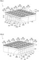
- Fig. 1 is a perspective view schematically illustrating a power storage module 1 according to an embodiment of the present disclosure.
- Fig. 2 is another perspective view schematically illustrating the power storage module 1 according to the embodiment of the present disclosure.
- the power storage module 1 according to an embodiment of the present disclosure includes two or more power storage cells 10, a band 20, and one or more bus bars 30.
- the two or more power storage cells 10 are arranged side by side in the lateral direction. Specifically, two or more power storage cells 10 are arranged side by side in the thickness direction of the power storage cell 10.
- a spacer (not illustrated) may be disposed between a pair of power storage cells 10 adjacent to each other.
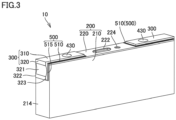
- Fig. 3 is a perspective view schematically illustrating the power storage cell according to an embodiment of the present disclosure.
- Fig. 4 is a cross-sectional view of the power storage module taken along line IV-IV in Fig. 1 .
- the power storage cell 10 includes an electrode assembly 100, a cell case 200, a pair of external terminals 300, a pair of connecting members 400, and an insulating member 500.
- Fig. 5 is a cross-sectional view of the electrode assembly taken along line V-V in Fig. 4 .
- the electrode assembly 100 includes a plurality of electrodes 110 and 120, and a separator 130.
- the plurality of electrodes 110 and 120 are arranged side by side in one direction (the lateral direction in Fig. 5 ).
- the plurality of electrodes 110 and 120 include a plurality of positive electrodes 110 and a plurality of negative electrodes 120.
- Each positive electrode 110 is formed in a rectangular shape elongated in a width direction (a direction orthogonal to both the one direction and the vertical direction).
- Each positive electrode 110 includes a positive electrode collector foil 112 and a positive electrode active material layer 114 provided on both surfaces of the positive electrode collector foil 112.
- the positive electrode collector foil 112 includes a positive electrode tab 112p (see Fig. 4 ) on which the positive electrode active material layer 114 is not provided.
- the positive electrode tab 112p protrudes toward one side of the width direction (a direction orthogonal to the paper surface of Fig. 5 ).
- Each negative electrode 120 is formed in a rectangular shape elongated in the width direction.
- Each negative electrode 120 includes a negative electrode collector foil 122 and a negative electrode active material layer 124 provided on both surfaces of the negative electrode collector foil 122.
- the negative electrode collector foil 122 includes a negative electrode tab 122n (see Fig. 4 ) on which the negative electrode active material layer 124 is not provided. The negative electrode tab 122n protrudes toward the other side of the width direction.
- the separator 130 insulates the positive electrode 110 and the negative electrode 120 from each other.
- the separator 130 is made of an insulating material, and has minute voids that allow ions to pass through. As illustrated in Fig. 5 , the separator 130 is formed in a zigzag shape.
- the separator 130 has a rectangular shape before being formed in a zigzag shape.
- the separator 130 is formed in a zigzag shape and is arranged between the electrodes 110 and 120.
- the separator 130 includes a plurality of intervening portions 132a, a plurality of upper folded portions 132b, a plurality of lower folded portions 132c, and an outermost covering portioning portion 132d.
- Each intervening portion 132a is interposed between a pair of electrodes 110 and 120 adjacent to each other in the one direction. In other words, each intervening portion 132a functions to insulate the positive electrode 110 and the negative electrode 120 from each other. Each intervening portion 132a is formed in a rectangular shape.
- Each upper folded portion 132b connects an upper end of one intervening portion 132a of the plurality of intervening portions 132a to an upper end of another intervening portion 132a of the plurality of intervening portions 132a which is adjacent to the one intervening portion 132a on one side of the one direction.
- the upper folded portion 132b is disposed above the positive electrode 110.
- Each lower folded portion 132c connects a lower end of one intervening portion 132a of the plurality of intervening portions 132a to a lower end of another intervening portion 132a of the plurality of intervening portions 132a which is adjacent to the one intervening portion 132a on the other side of the one direction.
- the lower folded portion 132c is disposed below the negative electrode 120.
- the negative electrode 120 is disposed above the lower folded portion 132c.
- the outermost covering portioning portion 132d collectively covers each upper folded portion 132b and each lower folded portion 132c. More specifically, the outermost covering portioning portion 132d collectively covers all of the electrodes 110 and 120, all of the intervening portions 132a, all of the upper folded portions 132b and all of the lower folded portions 132c while being wound around a central axis parallel to the width direction.
- a terminal end 132e of the outermost covering portioning portion 132d is configured not to overlap with the positive electrode active material layer 114 and the negative electrode active material layer 124 in the one direction. In the present embodiment, the terminal end 132e of the outermost covering portioning portion 132d is provided below each of the electrodes 110 and 120.
- the peripheral surface and bottom surface of the plurality of electrodes 110 and 120 and the separator 130 are covered with an insulating film (not illustrated).
- the cell case 200 houses the electrode assembly 100.
- the cell case 200 contains an electrolytic solution (not illustrated).
- the cell case 200 is sealed.
- the cell case 200 includes a case body 210 and a lid 220.
- the case body 210 has an opening that opens upward.
- the case body 210 is made of a metal such as aluminum.
- the case body 210 includes a bottom wall 212 and a peripheral wall 214.
- the bottom wall 212 is formed in a rectangular flat plate shape.
- the peripheral wall 214 rises from the bottom wall 212.
- the peripheral wall 214 is formed in a quadrangular cylindrical shape.
- the length of the peripheral wall 214 in the width direction is longer than the length of the peripheral wall 214 in the thickness direction.
- the length of the peripheral wall 214 in the height direction is longer than the length of the peripheral wall 214 in the thickness direction.
- the lid 220 closes the opening of the case body 210.
- the lid 220 is connected to the opening by welding or the like.
- the lid 220 is formed in a flat plate shape.
- the lid 220 is made of a metal such as aluminum.
- the lid 220 includes a pressure release valve 222 and a sealing member 224.
- the pressure release valve 222 is formed at a central portion of the lid 220.
- the pressure release valve 222 is configured to break when the internal pressure of the cell case 200 becomes equal to or higher than a predetermined pressure. When the pressure release valve 222 is broken, the gas in the cell case 200 is released to the outside of the cell case 200 through the pressure release valve 222, which reduces the internal pressure of the cell case 200.
- the sealing member 224 seals a liquid injection port h formed in the lid 220.
- the liquid injection port h is a through hole for injecting an electrolytic solution into the cell case 200 in the manufacturing process of the power storage cell 10. After the electrolytic solution is injected into the case body 210 through the liquid injection port h, the liquid injection port h is sealed by the sealing member 224.
- the pair of external terminals 300 is fixed to the cell case 200.
- One of the pair of external terminals 300 is a positive external terminal, and the other is a negative external terminal.
- Each external terminal 300 is fixed to an upper surface of the lid 220 via an upper insulating portion 510 which will be described later.
- Each external terminal 300 is made of a metal such as aluminum.
- Each external terminal 300 includes a first terminal portion 310 and a second terminal portion 320.
- the first terminal portion 310 is arranged above the cell case 200. More specifically, the first terminal portion 310 is fixed to the upper surface of the lid 220 via the upper insulating portion 510.
- the first terminal portion 310 is formed, for example, in a rectangular parallelepiped shape.
- the second terminal portion 320 extends from the first terminal portion 310 along a side surface of the cell case 200. More specifically, the second terminal portion 320 extends along the peripheral wall 214 in the thickness direction of the case body 210.
- the second terminal portion 320 is provided with a recess 321.
- the recess 321 is formed on a surface of the second terminal portion 320 opposite to the other surface thereof that faces the cell case 200 (the case body 210).
- the recess 321 extends from one end edge 322 to the other end edge 323 in the lateral direction of the second terminal portion 320 when viewed from the direction (i.e., the width direction) in which the second terminal portion 320 and the cell case 200 (the case body 210) are arranged in line (see Fig. 3 ).
- the pair of connecting members 400 connects a plurality of electrode tabs 112p and a plurality of electrode tabs 122n to the pair of external terminals 300, respectively. More specifically, one of the pair of connecting members 400 connects the plurality of positive electrode tabs 112p to the positive external terminal300, and the other connecting member 400 connects the plurality of negative electrode tabs 122n to the negative external terminal 300. Since the pair of connecting members 400 have substantially the same structure, only one connecting member 400 will be described below.
- the connecting member 400 includes a collector tab 410, a subtab 420, and a connecting pin 430.
- the collector tab 410 has a side portion 412 and an upper portion 414.
- the side portion 412 is arranged on a side surface of the electrode assembly 100 in the width direction.
- the upper portion 414 is arranged above an upper surface of the electrode assembly 100.
- the upper portion 414 extends inward in the width direction from an upper end of the side portion 412.
- the subtab 420 connects the plurality of positive electrode tabs 112p to the collector tab 410.
- One end 422 of the subtab 420 is connected to the plurality of positive electrode tabs 112p by welding or the like, and the other end 424 of the subtab 420 is connected to the side portion 412 of the collector tab 410 by welding or the like.
- the connecting pin 430 connects the collector tab 410 to the first terminal portion 310 of the external terminal 300.
- the connecting pin 430 connects the upper portion 414 to the first terminal portion 310 of the external terminal 300.
- the lower end of the connecting pin 430 is inserted into a through hole provided on the upper portion 414 and is connected to the upper portion 414 by welding or the like
- the upper end of the connecting pin 430 is inserted into a through hole provided on the first terminal portion 310 of the external terminal 300 and is connected to the external terminal 300 by welding, caulking or the like.
- the insulating member 500 insulates the cell case 200 and the connecting member 400 from each other.
- the insulating member 500 includes an upper insulating portion 510, a lateral insulating portion 515, a lower insulating portion 520, an insulating cylinder 530, and an insulating plate 540.
- the upper insulating portion 510 is fixed to the upper surface of the lid 220.
- the upper insulating portion 510 is disposed between the lid 220 and the first terminal portion 310 of the external terminal 300.
- the upper insulating portion 510 is provided with an insertion hole through which the connecting pin 430 is inserted.
- the lateral insulating portion 515 is disposed on the peripheral wall 214 of the case body 210.
- the lateral insulating portion 515 extends downward from the upper insulating portion 510.
- the lateral insulating portion 515 is disposed between the peripheral wall 214 of the case body 210 and the second terminal portion 320 of the external terminal 300.
- the lower insulating portion 520 is fixed to the lower surface of the lid 220.
- the lower insulating portion 520 is disposed between the lid 220, and the upper portion 414 and a lower portion of the connecting pin 430.
- the lower insulating portion 520 is provided with an insertion hole through which the connecting pin 430 is inserted.
- the insulating cylinder 530 is disposed between the connecting pin 430 and the lid 220.
- the insulating cylinder 530 is formed in a cylindrical shape, and is configured to surround the connecting pin 430.
- the insulating plate 540 is fixed to the lower surface of the upper portion 414.
- the insulating plate 540 is disposed on the electrode assembly 100.
- a through hole is formed in a portion of the insulating plate 540 located below the pressure release valve 222 and a portion of the insulating plate 540 located below the liquid injection port h.
- the insulating member 500 insulating one connecting member 400 (for example, the connecting member 400 electrically connected to the positive tab 112p) of the pair of connecting members 400 and the cell case 200 may not include the upper insulating section 510 and the lateral insulating section 515.
- the external terminal 300 may be in direct contact with the cell case 200, or a conductive member may be disposed between the external terminal 300 and the cell case 200 instead of the upper insulating portion 510 and the lateral insulating portion 515.
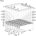
- Fig. 6 is a perspective view schematically illustrating a step of attaching a band to a plurality of power storage cells.
- the band 20 is configured to surround two or more power storage cells 10.
- the band 20 extends in a circular shape along the lateral direction orthogonal to the vertical direction.
- the band 20 has a belt-like profile.
- the band 20 is stretchable.
- the band 20 surrounds the power storage cells 10 in a stretched state.
- the band 20 restrains two or more power storage cells 10 by a contracting force.
- the band 20 is configured to further stretch from the state of surrounding the power storage cells 10.
- the material of the band 20 is not particularly limited.
- the band 20 may be made of an elastic material such as silicone rubber.
- the band 20 is constituted by one band member formed in a circular shape.
- the band 20 may be formed in a circular shape by connecting both ends of a belt member to each other.
- the band 20 may have a connection portion formed by connecting both ends to each other.
- the band 20 may be constituted by two or more belt members.
- the band 20 may be formed in a circular shape by connecting the ends of adjacent belt members to each other.
- the band 20 may have two or more connection portions formed by connecting the ends of two or more belt members to each other.
- connection portion the belt members constituting the band 20 may be separable from each other.
- the length of the band 20 in the circular direction may be adjustable at the connection portion. This makes it possible to easily modify the design of the band 20 when the shape of the power storage cells 10 or the number of the power storage cells 10 is changed.
- the connection portion may be configured as a belt buckle which allows to adjust the length of the band 20.
- the bus bar 30 (the first bus bar 30A) is disposed in the recess 321 of a first power storage cell 10A which is one of the two or more power storage cells 10 and in the recess 321 of a second power storage cell 10B which is another one of the two or more power storage cells 10 and is adjacent to the first power storage cell 10A.
- the bus bar 30 is electrically conductive. Therefore, the bus bar 30 electrically connects the external terminal 300 of the first power storage cell 10A and the external terminal 300 of the second power storage cell 10B.
- the bus bar 30 is made of a metal such as aluminum or an aluminum alloy.
- the bus bar 30 may be connected to the external terminals 300 by welding or the like.
- the two or more power storage cells 10 further include a third power storage cell 10C.
- the one or more bus bars 30 further include a second bus bar 30B different from the first bus bar 30A.
- the third power storage cell 10C is disposed on one side of the first power storage cell 10A opposite to the side where the second power storage cell 10B is disposed.
- the third power storage cell 10C is adjacent to the first power storage cell 10A.
- the second bus bar 30B is disposed in the recess 321 provided on the other side surface of the first power storage cell 10A and in the recess 321 of the third power storage cell 10C.
- the bus bar 30 is provided on a surface of the band 20 that faces the power storage cell 10. A portion of the bus bar 30 is embedded in the band 20.
- either the first bus bar 30A or the second bus bar 30B is provided on a surface of the band 20 that faces the power storage cell 10. More specifically, all the bus bars 30 positioned on the inner peripheral side of the band 20 are provided on the surface of the band 20 that faces the power storage cell 10. These bus bars 30 are fixed on the surface of the band 20. The bus bars 30 are spaced apart from each other on the surface of the band 20.
- the second terminal portion 320 is provided with a recess 321.
- the recess 321 is formed on a surface of the second terminal portion 320 opposite to the other surface thereof that faces the cell case 200.
- the position of the bus bar 30 with respect to the external terminal 300 may be determined by placing the bus bar 30 in the recess 321. Therefore, it is possible to easily determine the position of a component such as the bus bar for connecting the power storage cells 10 to each other.
- the recess 321 extends from one end edge 322 to the other end edge 323 in the lateral direction of the second terminal portion 320 when viewed from the direction in which the second terminal portion 320 and the cell case 200 are arranged in line.
- the bus bar 30 is slidable in the recess 321 in the thickness direction of the cell case 200. Therefore, it is possible to easily adjust the position of a component such as the bus bar 30 with respect to the second terminal portion 320 in the vertical direction, and it is possible to easily adjust the position of a component such as the bus bar 30 with respect to the second terminal portion 320 in the lateral direction. Therefore, it is possible to easily connect the power storage cells 10 to each other.
- the power storage module 1 includes two or more power storage cells 10, a band 20, and a bus bar 30.
- the two or more power storage cells 10 are arranged side by side in the lateral direction.
- the band 20 surrounds two or more power storage cells 10.
- the bus bar 30 is disposed in the recess 321 of the first power storage cell 10A, which is one of the two or more power storage cells 10, and in the recess 321 of the second power storage cell 10B, which is another one of the two or more power storage cells 10 and is adjacent to the first power storage cell 10A.
- the bus bar 30 is provided on a surface of the band 20 that faces the power storage cell 10.
- the above configuration it is possible to reduce the height of the power storage module 1 as compared with the case where the external terminals 300 are connected to each other by the bus bar on the upper surface of the external terminal 300. Further, by attaching the band 20 to the plurality of power storage cells 10 in the vertical direction (see Fig. 6 ), it is possible to easily dispose the bus bar 30 in each recess 321. Therefore, it is possible to easily connect the power storage cells 10 to each other.
- the band 20 is stretchable. According to this configuration, it is possible to restrain the plurality of power storage cells 10 by a contracting force of the band 20. Further, by restraining the power storage cell 10 with the band 20, it is possible to fix the bus bar 30 in the recess 321 before welding or without the need of welding the bus bar 30 to the external terminal 300. Further, by stretching the band 20, it is possible to easily detach the bus bar 30 from the recess 321. Therefore, it is possible to easily connect the power storage cells 10 to each other.
Landscapes
- Chemical & Material Sciences (AREA)
- Chemical Kinetics & Catalysis (AREA)
- Electrochemistry (AREA)
- General Chemical & Material Sciences (AREA)
- Connection Of Batteries Or Terminals (AREA)
- Battery Mounting, Suspending (AREA)
Abstract
Description
- This non-provisional application is based on
Japanese Patent Application No. 2023-079065 filed on May 12, 2023 - The present disclosure relates to a power storage cell and a power storage module.
- Conventionally,
US Patent Application Publication No. 2016/0372793 discloses a rechargeable battery. The rechargeable battery includes an electrode assembly, a case, a cap plate, a first sub-terminal, and a second sub-terminal. The cap plate seals an opening of the case. The first sub-terminal is arranged on one end of the cap plate, and extends adjacent to an outer surface of the case. The second sub-terminal is on the other end of the cap plate, and extends adjacent to another outer surface of the case. - In the rechargeable battery (i.e., the power storage cell) disclosed in
US Patent Application Publication No. 2016/0372793 , in order to reduce the height of the power storage module, the external terminals (i.e., the sub-terminals) of adj acent power storage cells are electrically connected to each other by a bus bar or the like on a side surface of the case. However, it is not easy to arrange the bus bar or the like with respect to the external terminal on the side surface of the case. - The present disclosure has been accomplished in view of the aforementioned problem, and it is therefore an object of the present disclosure to provide a power storage cell and a power storage module which allows an easy arrangement of a component such as a bus bar for connecting power storage cells to each other.
- The power storage cell according to the present disclosure includes an electrode assembly, a cell case, and an external terminal. The cell case houses an electrode assembly. The external terminal is fixed to the cell case. The external terminal includes a first terminal portion and a second terminal portion. The first terminal portion is arranged above the cell case. The second terminal portion extends from the first terminal portion along the side surface of the cell case. The second terminal portion is provided with a recess. The recess is formed on a surface of the second terminal portion opposite to the other surface thereof that faces the cell case.
- A power storage module according to an embodiment of the present disclosure includes two or more power storage cells, a band, and a bus bar. The two or more power storage cells are arranged side by side in the lateral direction. The band surrounds the two or more power storage cells. The bus bar is disposed in the recess of a first power storage cell which is one of the two or more power storage cells and in the recess of a second power storage cell which is another one of the two or more power storage cells and is adjacent to the first power storage cell. The bus bar is provided on a surface of the band that faces the power storage cell.
- The foregoing and other objects, features, aspects and advantages of the present disclosure will become more apparent from the following detailed description of the present disclosure when taken in conjunction with the accompanying drawings.
-
-
Fig. 1 is a perspective view schematically illustrating a power storage module according to an embodiment of the present disclosure; -
Fig. 2 is another perspective view schematically illustrating a power storage module according to an embodiment of the present disclosure; -
Fig. 3 is a perspective view schematically illustrating a power storage cell according to an embodiment of the present disclosure; -
Fig. 4 is a cross-sectional view of the power storage module taken along line IV-IV inFig. 1 ; -
Fig. 5 is a cross-sectional view of an electrode assembly taken along line V-V inFig. 4 ; and -
Fig. 6 is a perspective view schematically illustrating a step of attaching a band to a plurality of power storage cells. - Embodiments of the present disclosure will be described with reference to the drawings. In the following drawings, the same or corresponding members are denoted by the same reference numerals.
-
Fig. 1 is a perspective view schematically illustrating apower storage module 1 according to an embodiment of the present disclosure.Fig. 2 is another perspective view schematically illustrating thepower storage module 1 according to the embodiment of the present disclosure. As illustrated inFigs. 1 and 2 , thepower storage module 1 according to an embodiment of the present disclosure includes two or morepower storage cells 10, aband 20, and one ormore bus bars 30. - The two or more
power storage cells 10 are arranged side by side in the lateral direction. Specifically, two or morepower storage cells 10 are arranged side by side in the thickness direction of thepower storage cell 10. A spacer (not illustrated) may be disposed between a pair ofpower storage cells 10 adjacent to each other. - First, the configuration of the
power storage cell 10 will be described in detail.Fig. 3 is a perspective view schematically illustrating the power storage cell according to an embodiment of the present disclosure.Fig. 4 is a cross-sectional view of the power storage module taken along line IV-IV inFig. 1 . - As illustrated in
Figs. 3 and4 , thepower storage cell 10 includes anelectrode assembly 100, acell case 200, a pair ofexternal terminals 300, a pair of connectingmembers 400, and aninsulating member 500. -
Fig. 5 is a cross-sectional view of the electrode assembly taken along line V-V inFig. 4 . As illustrated inFig. 5 , theelectrode assembly 100 includes a plurality ofelectrodes separator 130. - As illustrated in
Fig. 5 , the plurality ofelectrodes Fig. 5 ). The plurality ofelectrodes positive electrodes 110 and a plurality ofnegative electrodes 120. - Each
positive electrode 110 is formed in a rectangular shape elongated in a width direction (a direction orthogonal to both the one direction and the vertical direction). Eachpositive electrode 110 includes a positive electrode collector foil 112 and a positive electrodeactive material layer 114 provided on both surfaces of the positive electrode collector foil 112. The positive electrode collector foil 112 includes apositive electrode tab 112p (seeFig. 4 ) on which the positive electrodeactive material layer 114 is not provided. Thepositive electrode tab 112p protrudes toward one side of the width direction (a direction orthogonal to the paper surface ofFig. 5 ). - Each
negative electrode 120 is formed in a rectangular shape elongated in the width direction. Eachnegative electrode 120 includes a negativeelectrode collector foil 122 and a negative electrodeactive material layer 124 provided on both surfaces of the negativeelectrode collector foil 122. As illustrated inFig. 4 , the negativeelectrode collector foil 122 includes anegative electrode tab 122n (seeFig. 4 ) on which the negative electrodeactive material layer 124 is not provided. Thenegative electrode tab 122n protrudes toward the other side of the width direction. - The
separator 130 insulates thepositive electrode 110 and thenegative electrode 120 from each other. Theseparator 130 is made of an insulating material, and has minute voids that allow ions to pass through. As illustrated inFig. 5 , theseparator 130 is formed in a zigzag shape. - The
separator 130 has a rectangular shape before being formed in a zigzag shape. Theseparator 130 is formed in a zigzag shape and is arranged between theelectrodes separator 130 includes a plurality of interveningportions 132a, a plurality of upper foldedportions 132b, a plurality of lower foldedportions 132c, and an outermostcovering portioning portion 132d. - Each intervening
portion 132a is interposed between a pair ofelectrodes portion 132a functions to insulate thepositive electrode 110 and thenegative electrode 120 from each other. Each interveningportion 132a is formed in a rectangular shape. - Each upper folded
portion 132b connects an upper end of one interveningportion 132a of the plurality of interveningportions 132a to an upper end of another interveningportion 132a of the plurality of interveningportions 132a which is adjacent to the one interveningportion 132a on one side of the one direction. In the present embodiment, the upper foldedportion 132b is disposed above thepositive electrode 110. - Each lower folded
portion 132c connects a lower end of one interveningportion 132a of the plurality of interveningportions 132a to a lower end of another interveningportion 132a of the plurality of interveningportions 132a which is adjacent to the one interveningportion 132a on the other side of the one direction. In the present embodiment, the lower foldedportion 132c is disposed below thenegative electrode 120. In other words, thenegative electrode 120 is disposed above the lower foldedportion 132c. - The outermost
covering portioning portion 132d collectively covers each upper foldedportion 132b and each lower foldedportion 132c. More specifically, the outermostcovering portioning portion 132d collectively covers all of theelectrodes portions 132a, all of the upper foldedportions 132b and all of the lower foldedportions 132c while being wound around a central axis parallel to the width direction. Aterminal end 132e of the outermostcovering portioning portion 132d is configured not to overlap with the positive electrodeactive material layer 114 and the negative electrodeactive material layer 124 in the one direction. In the present embodiment, theterminal end 132e of the outermostcovering portioning portion 132d is provided below each of theelectrodes electrodes separator 130 are covered with an insulating film (not illustrated). - As illustrated in
Figs. 3 and4 , thecell case 200 houses theelectrode assembly 100. Thecell case 200 contains an electrolytic solution (not illustrated). Thecell case 200 is sealed. Thecell case 200 includes acase body 210 and alid 220. - The
case body 210 has an opening that opens upward. Thecase body 210 is made of a metal such as aluminum. Thecase body 210 includes abottom wall 212 and aperipheral wall 214. Thebottom wall 212 is formed in a rectangular flat plate shape. Theperipheral wall 214 rises from thebottom wall 212. Theperipheral wall 214 is formed in a quadrangular cylindrical shape. The length of theperipheral wall 214 in the width direction is longer than the length of theperipheral wall 214 in the thickness direction. The length of theperipheral wall 214 in the height direction is longer than the length of theperipheral wall 214 in the thickness direction. - The
lid 220 closes the opening of thecase body 210. Thelid 220 is connected to the opening by welding or the like. Thelid 220 is formed in a flat plate shape. Thelid 220 is made of a metal such as aluminum. Thelid 220 includes apressure release valve 222 and a sealingmember 224. - The
pressure release valve 222 is formed at a central portion of thelid 220. Thepressure release valve 222 is configured to break when the internal pressure of thecell case 200 becomes equal to or higher than a predetermined pressure. When thepressure release valve 222 is broken, the gas in thecell case 200 is released to the outside of thecell case 200 through thepressure release valve 222, which reduces the internal pressure of thecell case 200. - The sealing
member 224 seals a liquid injection port h formed in thelid 220. The liquid injection port h is a through hole for injecting an electrolytic solution into thecell case 200 in the manufacturing process of thepower storage cell 10. After the electrolytic solution is injected into thecase body 210 through the liquid injection port h, the liquid injection port h is sealed by the sealingmember 224. - The pair of
external terminals 300 is fixed to thecell case 200. One of the pair ofexternal terminals 300 is a positive external terminal, and the other is a negative external terminal. Eachexternal terminal 300 is fixed to an upper surface of thelid 220 via an upper insulatingportion 510 which will be described later. Eachexternal terminal 300 is made of a metal such as aluminum. - Each
external terminal 300 includes a firstterminal portion 310 and a secondterminal portion 320. The firstterminal portion 310 is arranged above thecell case 200. More specifically, the firstterminal portion 310 is fixed to the upper surface of thelid 220 via the upper insulatingportion 510. The firstterminal portion 310 is formed, for example, in a rectangular parallelepiped shape. - The second
terminal portion 320 extends from the firstterminal portion 310 along a side surface of thecell case 200. More specifically, the secondterminal portion 320 extends along theperipheral wall 214 in the thickness direction of thecase body 210. - The second
terminal portion 320 is provided with arecess 321. Therecess 321 is formed on a surface of the secondterminal portion 320 opposite to the other surface thereof that faces the cell case 200 (the case body 210). Therecess 321 extends from oneend edge 322 to theother end edge 323 in the lateral direction of the secondterminal portion 320 when viewed from the direction (i.e., the width direction) in which the secondterminal portion 320 and the cell case 200 (the case body 210) are arranged in line (seeFig. 3 ). - The pair of connecting
members 400 connects a plurality ofelectrode tabs 112p and a plurality ofelectrode tabs 122n to the pair ofexternal terminals 300, respectively. More specifically, one of the pair of connectingmembers 400 connects the plurality ofpositive electrode tabs 112p to the positive external terminal300, and the other connectingmember 400 connects the plurality ofnegative electrode tabs 122n to the negativeexternal terminal 300. Since the pair of connectingmembers 400 have substantially the same structure, only one connectingmember 400 will be described below. - The connecting
member 400 includes acollector tab 410, asubtab 420, and a connectingpin 430. - The
collector tab 410 has aside portion 412 and anupper portion 414. Theside portion 412 is arranged on a side surface of theelectrode assembly 100 in the width direction. Theupper portion 414 is arranged above an upper surface of theelectrode assembly 100. Theupper portion 414 extends inward in the width direction from an upper end of theside portion 412. - The
subtab 420 connects the plurality ofpositive electrode tabs 112p to thecollector tab 410. Oneend 422 of thesubtab 420 is connected to the plurality ofpositive electrode tabs 112p by welding or the like, and theother end 424 of thesubtab 420 is connected to theside portion 412 of thecollector tab 410 by welding or the like. - The connecting
pin 430 connects thecollector tab 410 to the firstterminal portion 310 of theexternal terminal 300. The connectingpin 430 connects theupper portion 414 to the firstterminal portion 310 of theexternal terminal 300. Specifically, the lower end of the connectingpin 430 is inserted into a through hole provided on theupper portion 414 and is connected to theupper portion 414 by welding or the like, and the upper end of the connectingpin 430 is inserted into a through hole provided on the firstterminal portion 310 of theexternal terminal 300 and is connected to theexternal terminal 300 by welding, caulking or the like. - The insulating
member 500 insulates thecell case 200 and the connectingmember 400 from each other. The insulatingmember 500 includes an upper insulatingportion 510, a lateral insulatingportion 515, a lower insulatingportion 520, an insulatingcylinder 530, and an insulatingplate 540. - The upper insulating
portion 510 is fixed to the upper surface of thelid 220. The upper insulatingportion 510 is disposed between thelid 220 and the firstterminal portion 310 of theexternal terminal 300. The upper insulatingportion 510 is provided with an insertion hole through which the connectingpin 430 is inserted. - The lateral insulating
portion 515 is disposed on theperipheral wall 214 of thecase body 210. The lateral insulatingportion 515 extends downward from the upper insulatingportion 510. The lateral insulatingportion 515 is disposed between theperipheral wall 214 of thecase body 210 and the secondterminal portion 320 of theexternal terminal 300. - The lower insulating
portion 520 is fixed to the lower surface of thelid 220. The lower insulatingportion 520 is disposed between thelid 220, and theupper portion 414 and a lower portion of the connectingpin 430. The lower insulatingportion 520 is provided with an insertion hole through which the connectingpin 430 is inserted. - The insulating
cylinder 530 is disposed between the connectingpin 430 and thelid 220. The insulatingcylinder 530 is formed in a cylindrical shape, and is configured to surround the connectingpin 430. - The insulating
plate 540 is fixed to the lower surface of theupper portion 414. The insulatingplate 540 is disposed on theelectrode assembly 100. A through hole is formed in a portion of the insulatingplate 540 located below thepressure release valve 222 and a portion of the insulatingplate 540 located below the liquid injection port h. - The insulating
member 500 insulating one connecting member 400 (for example, the connectingmember 400 electrically connected to thepositive tab 112p) of the pair of connectingmembers 400 and thecell case 200 may not include the upper insulatingsection 510 and the lateral insulatingsection 515. In this case, theexternal terminal 300 may be in direct contact with thecell case 200, or a conductive member may be disposed between theexternal terminal 300 and thecell case 200 instead of the upper insulatingportion 510 and the lateral insulatingportion 515. - Next, the
band 20 and thebus bar 30 of thepower storage module 1 will be described.Fig. 6 is a perspective view schematically illustrating a step of attaching a band to a plurality of power storage cells. - As illustrated in
Figs. 1, 2 ,4 and6 , theband 20 is configured to surround two or morepower storage cells 10. Theband 20 extends in a circular shape along the lateral direction orthogonal to the vertical direction. Theband 20 has a belt-like profile. - The
band 20 is stretchable. Theband 20 surrounds thepower storage cells 10 in a stretched state. When theband 20 surrounds thepower storage cells 10, theband 20 restrains two or morepower storage cells 10 by a contracting force. Theband 20 is configured to further stretch from the state of surrounding thepower storage cells 10. The material of theband 20 is not particularly limited. Theband 20 may be made of an elastic material such as silicone rubber. - In the present embodiment, the
band 20 is constituted by one band member formed in a circular shape. However, theband 20 may be formed in a circular shape by connecting both ends of a belt member to each other. In other words, theband 20 may have a connection portion formed by connecting both ends to each other. - The
band 20 may be constituted by two or more belt members. In this case, theband 20 may be formed in a circular shape by connecting the ends of adjacent belt members to each other. In other words, theband 20 may have two or more connection portions formed by connecting the ends of two or more belt members to each other. - In the connection portion, the belt members constituting the
band 20 may be separable from each other. The length of theband 20 in the circular direction may be adjustable at the connection portion. This makes it possible to easily modify the design of theband 20 when the shape of thepower storage cells 10 or the number of thepower storage cells 10 is changed. The connection portion may be configured as a belt buckle which allows to adjust the length of theband 20. - The bus bar 30 (the
first bus bar 30A) is disposed in therecess 321 of a firstpower storage cell 10A which is one of the two or morepower storage cells 10 and in therecess 321 of a secondpower storage cell 10B which is another one of the two or morepower storage cells 10 and is adjacent to the firstpower storage cell 10A. - The
bus bar 30 is electrically conductive. Therefore, thebus bar 30 electrically connects theexternal terminal 300 of the firstpower storage cell 10A and theexternal terminal 300 of the secondpower storage cell 10B. Thebus bar 30 is made of a metal such as aluminum or an aluminum alloy. Thebus bar 30 may be connected to theexternal terminals 300 by welding or the like. - In the present embodiment, the two or more
power storage cells 10 further include a thirdpower storage cell 10C. The one ormore bus bars 30 further include asecond bus bar 30B different from thefirst bus bar 30A. - The third
power storage cell 10C is disposed on one side of the firstpower storage cell 10A opposite to the side where the secondpower storage cell 10B is disposed. The thirdpower storage cell 10C is adjacent to the firstpower storage cell 10A. Thesecond bus bar 30B is disposed in therecess 321 provided on the other side surface of the firstpower storage cell 10A and in therecess 321 of the thirdpower storage cell 10C. - The
bus bar 30 is provided on a surface of theband 20 that faces thepower storage cell 10. A portion of thebus bar 30 is embedded in theband 20. - In the present embodiment, either the
first bus bar 30A or thesecond bus bar 30B is provided on a surface of theband 20 that faces thepower storage cell 10. More specifically, all the bus bars 30 positioned on the inner peripheral side of theband 20 are provided on the surface of theband 20 that faces thepower storage cell 10. These bus bars 30 are fixed on the surface of theband 20. The bus bars 30 are spaced apart from each other on the surface of theband 20. - As described above, in the
power storage cell 10 according to the embodiment of the present disclosure, the secondterminal portion 320 is provided with arecess 321. Therecess 321 is formed on a surface of the secondterminal portion 320 opposite to the other surface thereof that faces thecell case 200. - According to the above configuration, the position of the
bus bar 30 with respect to theexternal terminal 300 may be determined by placing thebus bar 30 in therecess 321. Therefore, it is possible to easily determine the position of a component such as the bus bar for connecting thepower storage cells 10 to each other. - The
recess 321 extends from oneend edge 322 to theother end edge 323 in the lateral direction of the secondterminal portion 320 when viewed from the direction in which the secondterminal portion 320 and thecell case 200 are arranged in line. - According to the above configuration, the
bus bar 30 is slidable in therecess 321 in the thickness direction of thecell case 200. Therefore, it is possible to easily adjust the position of a component such as thebus bar 30 with respect to the secondterminal portion 320 in the vertical direction, and it is possible to easily adjust the position of a component such as thebus bar 30 with respect to the secondterminal portion 320 in the lateral direction. Therefore, it is possible to easily connect thepower storage cells 10 to each other. - The
power storage module 1 according to an embodiment of the present disclosure includes two or morepower storage cells 10, aband 20, and abus bar 30. The two or morepower storage cells 10 are arranged side by side in the lateral direction. Theband 20 surrounds two or morepower storage cells 10. Thebus bar 30 is disposed in therecess 321 of the firstpower storage cell 10A, which is one of the two or morepower storage cells 10, and in therecess 321 of the secondpower storage cell 10B, which is another one of the two or morepower storage cells 10 and is adjacent to the firstpower storage cell 10A. Thebus bar 30 is provided on a surface of theband 20 that faces thepower storage cell 10. - According to the above configuration, it is possible to reduce the height of the
power storage module 1 as compared with the case where theexternal terminals 300 are connected to each other by the bus bar on the upper surface of theexternal terminal 300. Further, by attaching theband 20 to the plurality ofpower storage cells 10 in the vertical direction (seeFig. 6 ), it is possible to easily dispose thebus bar 30 in eachrecess 321. Therefore, it is possible to easily connect thepower storage cells 10 to each other. - The
band 20 is stretchable. According to this configuration, it is possible to restrain the plurality ofpower storage cells 10 by a contracting force of theband 20. Further, by restraining thepower storage cell 10 with theband 20, it is possible to fix thebus bar 30 in therecess 321 before welding or without the need of welding thebus bar 30 to theexternal terminal 300. Further, by stretching theband 20, it is possible to easily detach thebus bar 30 from therecess 321. Therefore, it is possible to easily connect thepower storage cells 10 to each other. - Although the present disclosure has been described and illustrated in detail, it is clearly understood that the same is by way of illustration and example only and is not to be taken by way of limitation, the scope of the present disclosure being interpreted by the terms of the appended claims.
Claims (4)
- A power storage cell comprising:an electrode assembly (100);a cell case (200) that houses the electrode assembly (100); andan external terminal (300) that is fixed to the cell case (200),wherein the external terminal (300) includes a first terminal portion (310) that is arranged above the cell case (200), and a second terminal portion (320) that extends from the first terminal portion (310) along a side surface of the cell case (200),the second terminal portion (320) is provided with a recess (321) on a surface of the second terminal portion (320) opposite to the other surface thereof that faces the cell case (200).
- The power storage cell according to claim 1, wherein
the recess (321) extends from one end edge (322) to the other end edge (323) in a lateral direction of the second terminal portion (320) when viewed from a direction in which the second terminal portion (320) and the cell case (200) are arranged in line. - A power storage module comprising:two or more power storage cells (10) according to claim 1 or 2 that are arranged side by side in the lateral direction;a band (20) that surrounds the two or more power storage cells (10); anda bus bar (30) that is disposed in the recess (321) of a first power storage cell (10A) which is one of the two or more power storage cells (10) and in the recess (321) of a second power storage cell (10B) which is another one of the two or more power storage cells (10) and is adjacent to the first power storage cell (10A),the bus bar (30) is provided on a surface of the band (20) that faces the power storage cell (10).
- The power storage module according to claim 3, wherein
the band (20) is stretchable.
Applications Claiming Priority (1)
| Application Number | Priority Date | Filing Date | Title |
|---|---|---|---|
| JP2023079065A JP7772024B2 (en) | 2023-05-12 | 2023-05-12 | Energy storage cells and modules |
Publications (2)
| Publication Number | Publication Date |
|---|---|
| EP4462561A1 true EP4462561A1 (en) | 2024-11-13 |
| EP4462561B1 EP4462561B1 (en) | 2025-03-05 |
Family
ID=90366485
Family Applications (1)
| Application Number | Title | Priority Date | Filing Date |
|---|---|---|---|
| EP24164037.4A Active EP4462561B1 (en) | 2023-05-12 | 2024-03-18 | Power storage cell and power storage module |
Country Status (5)
| Country | Link |
|---|---|
| US (1) | US20240380081A1 (en) |
| EP (1) | EP4462561B1 (en) |
| JP (1) | JP7772024B2 (en) |
| KR (1) | KR20240164426A (en) |
| CN (1) | CN118943631A (en) |
Citations (4)
| Publication number | Priority date | Publication date | Assignee | Title |
|---|---|---|---|---|
| EP2654099A1 (en) * | 2010-12-13 | 2013-10-23 | Panasonic Corporation | Battery module and battery pack |
| CN103840190A (en) * | 2012-11-23 | 2014-06-04 | 三星Sdi株式会社 | Rechargeable battery and module of the same |
| CN104466220A (en) * | 2013-09-13 | 2015-03-25 | 三星Sdi株式会社 | Secondary battery module |
| US20160372793A1 (en) | 2015-06-22 | 2016-12-22 | Samsung Sdi Co., Ltd. | Rechargeable battery and rechargeable battery module |
Family Cites Families (7)
| Publication number | Priority date | Publication date | Assignee | Title |
|---|---|---|---|---|
| JP2004362826A (en) | 2003-06-02 | 2004-12-24 | Auto Network Gijutsu Kenkyusho:Kk | Battery device |
| JP5225805B2 (en) | 2008-10-27 | 2013-07-03 | 日立ビークルエナジー株式会社 | Secondary battery and manufacturing method thereof |
| KR101174897B1 (en) | 2010-10-12 | 2012-08-17 | 삼성에스디아이 주식회사 | battery assembly |
| KR101244739B1 (en) | 2011-05-09 | 2013-03-18 | 로베르트 보쉬 게엠베하 | Battery module |
| JP6148555B2 (en) | 2013-07-16 | 2017-06-14 | 株式会社ジーエスエレテック | Busbar module device |
| KR20160051476A (en) | 2014-11-03 | 2016-05-11 | 삼성에스디아이 주식회사 | Rechargeable battery and rechargeable battery pack including the same |
| KR20240060271A (en) | 2022-10-28 | 2024-05-08 | 주식회사 엘지에너지솔루션 | Secondary battery having improved terminal structure |
-
2023
- 2023-05-12 JP JP2023079065A patent/JP7772024B2/en active Active
-
2024
- 2024-03-18 EP EP24164037.4A patent/EP4462561B1/en active Active
- 2024-03-27 US US18/618,045 patent/US20240380081A1/en active Pending
- 2024-05-07 CN CN202410551250.8A patent/CN118943631A/en active Pending
- 2024-05-08 KR KR1020240060496A patent/KR20240164426A/en active Pending
Patent Citations (4)
| Publication number | Priority date | Publication date | Assignee | Title |
|---|---|---|---|---|
| EP2654099A1 (en) * | 2010-12-13 | 2013-10-23 | Panasonic Corporation | Battery module and battery pack |
| CN103840190A (en) * | 2012-11-23 | 2014-06-04 | 三星Sdi株式会社 | Rechargeable battery and module of the same |
| CN104466220A (en) * | 2013-09-13 | 2015-03-25 | 三星Sdi株式会社 | Secondary battery module |
| US20160372793A1 (en) | 2015-06-22 | 2016-12-22 | Samsung Sdi Co., Ltd. | Rechargeable battery and rechargeable battery module |
Also Published As
| Publication number | Publication date |
|---|---|
| KR20240164426A (en) | 2024-11-19 |
| JP7772024B2 (en) | 2025-11-18 |
| JP2024163458A (en) | 2024-11-22 |
| US20240380081A1 (en) | 2024-11-14 |
| EP4462561B1 (en) | 2025-03-05 |
| CN118943631A (en) | 2024-11-12 |
Similar Documents
| Publication | Publication Date | Title |
|---|---|---|
| KR100551396B1 (en) | Secondary battery having an integrated cap assembly and a method of forming an integrated cap assembly | |
| EP2228853B1 (en) | Rechargeable battery | |
| US10923703B2 (en) | Electricity storage apparatus | |
| EP2597705B1 (en) | Rechargeable battery | |
| US20090317665A1 (en) | Secondary battery | |
| US9028993B2 (en) | Secondary battery | |
| US12614811B2 (en) | Secondary battery | |
| US9059456B2 (en) | Rechargeable battery and battery module | |
| CN111566846B (en) | Secondary battery | |
| KR101621094B1 (en) | Secondary Battery | |
| KR20160100673A (en) | Battery pack | |
| US20120208075A1 (en) | Secondary Battery | |
| EP4462561B1 (en) | Power storage cell and power storage module | |
| US8993152B2 (en) | Rechargeable battery with terminal through-out portion, terminal plate, and fastening portion | |
| US20240154274A1 (en) | Power storage cell, and method of short-circuiting between lid and external terminal | |
| JP7852571B2 (en) | Secondary batteries and battery modules | |
| KR19990041761A (en) | Secondary battery cap assembly and assembly method | |
| US20240128617A1 (en) | Power storage cell | |
| US20240421392A1 (en) | Power storage cell | |
| EP4462533B1 (en) | Electrode assembly | |
| US20240421444A1 (en) | Power storage cell | |
| US20240396174A1 (en) | Power storage cell | |
| JP7810153B2 (en) | Energy storage module | |
| US20240128559A1 (en) | Method of manufacturing power storage cell and power storage cell | |
| US20250015397A1 (en) | Method of manufacturing battery case |
Legal Events
| Date | Code | Title | Description |
|---|---|---|---|
| PUAI | Public reference made under article 153(3) epc to a published international application that has entered the european phase |
Free format text: ORIGINAL CODE: 0009012 |
|
| STAA | Information on the status of an ep patent application or granted ep patent |
Free format text: STATUS: REQUEST FOR EXAMINATION WAS MADE |
|
| 17P | Request for examination filed |
Effective date: 20240318 |
|
| AK | Designated contracting states |
Kind code of ref document: A1 Designated state(s): AL AT BE BG CH CY CZ DE DK EE ES FI FR GB GR HR HU IE IS IT LI LT LU LV MC ME MK MT NL NO PL PT RO RS SE SI SK SM TR |
|
| GRAP | Despatch of communication of intention to grant a patent |
Free format text: ORIGINAL CODE: EPIDOSNIGR1 |
|
| STAA | Information on the status of an ep patent application or granted ep patent |
Free format text: STATUS: GRANT OF PATENT IS INTENDED |
|
| RIC1 | Information provided on ipc code assigned before grant |
Ipc: H01M 50/553 20210101ALI20241119BHEP Ipc: H01M 50/55 20210101ALI20241119BHEP Ipc: H01M 50/507 20210101ALI20241119BHEP Ipc: H01M 50/211 20210101ALI20241119BHEP Ipc: H01M 50/209 20210101AFI20241119BHEP |
|
| INTG | Intention to grant announced |
Effective date: 20241209 |
|
| GRAS | Grant fee paid |
Free format text: ORIGINAL CODE: EPIDOSNIGR3 |
|
| GRAA | (expected) grant |
Free format text: ORIGINAL CODE: 0009210 |
|
| STAA | Information on the status of an ep patent application or granted ep patent |
Free format text: STATUS: THE PATENT HAS BEEN GRANTED |
|
| AK | Designated contracting states |
Kind code of ref document: B1 Designated state(s): AL AT BE BG CH CY CZ DE DK EE ES FI FR GB GR HR HU IE IS IT LI LT LU LV MC ME MK MT NL NO PL PT RO RS SE SI SK SM TR |
|
| REG | Reference to a national code |
Ref country code: GB Ref legal event code: FG4D |
|
| REG | Reference to a national code |
Ref country code: CH Ref legal event code: EP |
|
| REG | Reference to a national code |
Ref country code: DE Ref legal event code: R096 Ref document number: 602024000023 Country of ref document: DE |
|
| REG | Reference to a national code |
Ref country code: IE Ref legal event code: FG4D |
|
| P01 | Opt-out of the competence of the unified patent court (upc) registered |
Free format text: CASE NUMBER: APP_20540/2025 Effective date: 20250430 |
|
| PG25 | Lapsed in a contracting state [announced via postgrant information from national office to epo] |
Ref country code: RS Free format text: LAPSE BECAUSE OF FAILURE TO SUBMIT A TRANSLATION OF THE DESCRIPTION OR TO PAY THE FEE WITHIN THE PRESCRIBED TIME-LIMIT Effective date: 20250605 |
|
| PG25 | Lapsed in a contracting state [announced via postgrant information from national office to epo] |
Ref country code: FI Free format text: LAPSE BECAUSE OF FAILURE TO SUBMIT A TRANSLATION OF THE DESCRIPTION OR TO PAY THE FEE WITHIN THE PRESCRIBED TIME-LIMIT Effective date: 20250305 |
|
| REG | Reference to a national code |
Ref country code: NL Ref legal event code: MP Effective date: 20250305 |
|
| PG25 | Lapsed in a contracting state [announced via postgrant information from national office to epo] |
Ref country code: ES Free format text: LAPSE BECAUSE OF FAILURE TO SUBMIT A TRANSLATION OF THE DESCRIPTION OR TO PAY THE FEE WITHIN THE PRESCRIBED TIME-LIMIT Effective date: 20250305 |
|
| REG | Reference to a national code |
Ref country code: LT Ref legal event code: MG9D |
|
| PG25 | Lapsed in a contracting state [announced via postgrant information from national office to epo] |
Ref country code: NO Free format text: LAPSE BECAUSE OF FAILURE TO SUBMIT A TRANSLATION OF THE DESCRIPTION OR TO PAY THE FEE WITHIN THE PRESCRIBED TIME-LIMIT Effective date: 20250605 |
|
| PG25 | Lapsed in a contracting state [announced via postgrant information from national office to epo] |
Ref country code: HR Free format text: LAPSE BECAUSE OF FAILURE TO SUBMIT A TRANSLATION OF THE DESCRIPTION OR TO PAY THE FEE WITHIN THE PRESCRIBED TIME-LIMIT Effective date: 20250305 |
|
| PG25 | Lapsed in a contracting state [announced via postgrant information from national office to epo] |
Ref country code: LV Free format text: LAPSE BECAUSE OF FAILURE TO SUBMIT A TRANSLATION OF THE DESCRIPTION OR TO PAY THE FEE WITHIN THE PRESCRIBED TIME-LIMIT Effective date: 20250305 |
|
| PG25 | Lapsed in a contracting state [announced via postgrant information from national office to epo] |
Ref country code: GR Free format text: LAPSE BECAUSE OF FAILURE TO SUBMIT A TRANSLATION OF THE DESCRIPTION OR TO PAY THE FEE WITHIN THE PRESCRIBED TIME-LIMIT Effective date: 20250606 Ref country code: BG Free format text: LAPSE BECAUSE OF FAILURE TO SUBMIT A TRANSLATION OF THE DESCRIPTION OR TO PAY THE FEE WITHIN THE PRESCRIBED TIME-LIMIT Effective date: 20250305 |
|
| PG25 | Lapsed in a contracting state [announced via postgrant information from national office to epo] |
Ref country code: NL Free format text: LAPSE BECAUSE OF FAILURE TO SUBMIT A TRANSLATION OF THE DESCRIPTION OR TO PAY THE FEE WITHIN THE PRESCRIBED TIME-LIMIT Effective date: 20250305 |
|
| PG25 | Lapsed in a contracting state [announced via postgrant information from national office to epo] |
Ref country code: SE Free format text: LAPSE BECAUSE OF FAILURE TO SUBMIT A TRANSLATION OF THE DESCRIPTION OR TO PAY THE FEE WITHIN THE PRESCRIBED TIME-LIMIT Effective date: 20250305 |
|
| REG | Reference to a national code |
Ref country code: DE Ref legal event code: R084 Ref document number: 602024000023 Country of ref document: DE |
|
| PG25 | Lapsed in a contracting state [announced via postgrant information from national office to epo] |
Ref country code: SM Free format text: LAPSE BECAUSE OF FAILURE TO SUBMIT A TRANSLATION OF THE DESCRIPTION OR TO PAY THE FEE WITHIN THE PRESCRIBED TIME-LIMIT Effective date: 20250305 |
|
| PG25 | Lapsed in a contracting state [announced via postgrant information from national office to epo] |
Ref country code: PT Free format text: LAPSE BECAUSE OF FAILURE TO SUBMIT A TRANSLATION OF THE DESCRIPTION OR TO PAY THE FEE WITHIN THE PRESCRIBED TIME-LIMIT Effective date: 20250707 |
|
| PG25 | Lapsed in a contracting state [announced via postgrant information from national office to epo] |
Ref country code: IT Free format text: LAPSE BECAUSE OF FAILURE TO SUBMIT A TRANSLATION OF THE DESCRIPTION OR TO PAY THE FEE WITHIN THE PRESCRIBED TIME-LIMIT Effective date: 20250305 Ref country code: PL Free format text: LAPSE BECAUSE OF FAILURE TO SUBMIT A TRANSLATION OF THE DESCRIPTION OR TO PAY THE FEE WITHIN THE PRESCRIBED TIME-LIMIT Effective date: 20250305 |
|
| PG25 | Lapsed in a contracting state [announced via postgrant information from national office to epo] |
Ref country code: AT Free format text: LAPSE BECAUSE OF FAILURE TO SUBMIT A TRANSLATION OF THE DESCRIPTION OR TO PAY THE FEE WITHIN THE PRESCRIBED TIME-LIMIT Effective date: 20250305 |
|
| PG25 | Lapsed in a contracting state [announced via postgrant information from national office to epo] |
Ref country code: EE Free format text: LAPSE BECAUSE OF FAILURE TO SUBMIT A TRANSLATION OF THE DESCRIPTION OR TO PAY THE FEE WITHIN THE PRESCRIBED TIME-LIMIT Effective date: 20250305 Ref country code: CZ Free format text: LAPSE BECAUSE OF FAILURE TO SUBMIT A TRANSLATION OF THE DESCRIPTION OR TO PAY THE FEE WITHIN THE PRESCRIBED TIME-LIMIT Effective date: 20250305 |
|
| PG25 | Lapsed in a contracting state [announced via postgrant information from national office to epo] |
Ref country code: SK Free format text: LAPSE BECAUSE OF FAILURE TO SUBMIT A TRANSLATION OF THE DESCRIPTION OR TO PAY THE FEE WITHIN THE PRESCRIBED TIME-LIMIT Effective date: 20250305 |
|
| PG25 | Lapsed in a contracting state [announced via postgrant information from national office to epo] |
Ref country code: IS Free format text: LAPSE BECAUSE OF FAILURE TO SUBMIT A TRANSLATION OF THE DESCRIPTION OR TO PAY THE FEE WITHIN THE PRESCRIBED TIME-LIMIT Effective date: 20250705 |
|
| REG | Reference to a national code |
Ref country code: DE Ref legal event code: R097 Ref document number: 602024000023 Country of ref document: DE |
|
| PG25 | Lapsed in a contracting state [announced via postgrant information from national office to epo] |
Ref country code: MC Free format text: LAPSE BECAUSE OF FAILURE TO SUBMIT A TRANSLATION OF THE DESCRIPTION OR TO PAY THE FEE WITHIN THE PRESCRIBED TIME-LIMIT Effective date: 20250305 |
|
| PLBE | No opposition filed within time limit |
Free format text: ORIGINAL CODE: 0009261 |
|
| STAA | Information on the status of an ep patent application or granted ep patent |
Free format text: STATUS: NO OPPOSITION FILED WITHIN TIME LIMIT |
|
| PG25 | Lapsed in a contracting state [announced via postgrant information from national office to epo] |
Ref country code: DK Free format text: LAPSE BECAUSE OF FAILURE TO SUBMIT A TRANSLATION OF THE DESCRIPTION OR TO PAY THE FEE WITHIN THE PRESCRIBED TIME-LIMIT Effective date: 20250305 |
|
| REG | Reference to a national code |
Ref country code: CH Ref legal event code: L10 Free format text: ST27 STATUS EVENT CODE: U-0-0-L10-L00 (AS PROVIDED BY THE NATIONAL OFFICE) Effective date: 20260114 |
|
| 26N | No opposition filed |
Effective date: 20251208 |
|
| PGFP | Annual fee paid to national office [announced via postgrant information from national office to epo] |
Ref country code: DE Payment date: 20260128 Year of fee payment: 3 |
|
| PGFP | Annual fee paid to national office [announced via postgrant information from national office to epo] |
Ref country code: FR Payment date: 20260209 Year of fee payment: 3 |