EP4462467A1 - Verfahren zur herstellung von halbleiteranordnungen - Google Patents
Verfahren zur herstellung von halbleiteranordnungen Download PDFInfo
- Publication number
- EP4462467A1 EP4462467A1 EP24169742.4A EP24169742A EP4462467A1 EP 4462467 A1 EP4462467 A1 EP 4462467A1 EP 24169742 A EP24169742 A EP 24169742A EP 4462467 A1 EP4462467 A1 EP 4462467A1
- Authority
- EP
- European Patent Office
- Prior art keywords
- connecting bars
- electrically conductive
- insulating material
- conductive substrate
- common electrically
- Prior art date
- Legal status (The legal status is an assumption and is not a legal conclusion. Google has not performed a legal analysis and makes no representation as to the accuracy of the status listed.)
- Granted
Links
Images


Classifications
-
- H10W70/048—
-
- H10W70/457—
-
- H10W74/014—
-
- H10W70/424—
-
- H10W72/0198—
-
- H10W74/00—
-
- H10W90/755—
Definitions
- the description relates to manufacturing semiconductor devices.
- Wettable flanks are a desirable feature of integrated circuits semiconductor devices in as much as they enhance solderability of the devices to the final substrate, such as a printed circuit board (PCB), for instance.
- PCB printed circuit board
- wettable flanks facilitate automatic optical inspection (AOI) thanks to the formation of a solder meniscus at the flank of the device when soldered to the final substrate.
- AOI automatic optical inspection
- wettable flanks are conventionally provided via a "half-cut" at the connecting bars which run along the periphery of each individual device.
- a plurality of substrates (leadframes) for individual devices are held together in a leadframe strip using metallic connecting structures including (sacrificial) connecting bars running along the periphery of each device. Multiple devices are thus concurrently processed and finally singulated into individual devices.
- a plating step can be performed in order to plate the leadframe bottom surface with a metallic (solderable) layer, of tin, for instance.
- the "half-cut" may cause the connecting bars to be exposed at the surface of the leadframe strip during the plating step causing the connecting bars to be plated with a relatively large amount of tin.
- a singulating blade removes the connecting bars and the solderable metallic layer plated thereon. Due to the amount of metal accumulated on the connecting bars, the action of the blade during the singulation step may produce flakes or filaments that undesirably "bridge" neighboring leads causing a short circuit therebetween.
- Document EP 4 057 342 A2 discloses a semiconductor device, such as a QFN (Quad-Flat No-lead) package, that comprises one or mode semiconductor chips arranged on a surface of a leadframe.
- the semiconductor chip(s) is/are arranged at a die pad of the leadframe and the leadframe has an array of electrically-conductive leads around the die pad.
- the leads in the array have distal ends facing away from the die pad as well as recessed portions of the surface of the leadframe at the distal ends of the leads in the array.
- Resilient material such as low elasticity modulus material is formed at the recessed portions at the distal ends of the leads in the array, and an insulating encapsulation is molded onto the semiconductor chip(s) arranged on the leadframe.
- the resilient material is sandwiched between the insulating encapsulation and the distal ends of the leads in the array at the recessed portions and facilitates flexibility of the leads, making them suited for reliable soldering to an insulated metal substrate.
- the resilient material is jetted on the upper side of the leads -- before molding.
- Document EP 2 680 307 A2 discloses a structure and method to improve saw singulation quality and wettability of integrated circuit packages assembled with lead frames having half-etched recesses in leads.
- a method of forming a semiconductor device package includes providing a lead frame strip having a plurality of lead frames. Each of the lead frames includes a depression that is at least partially filled with a material prior to singulating the strip.
- Document EP 4 099 368 A1 discloses a method of manufacturing semiconductor devices, such as "die pad up" QFN (Quad-Flat No-lead) packages, comprises arranging a plurality of semiconductor chips on an elongated substrate and providing an insulating encapsulation of the semiconductor chips. Electrically conductive formations are plated on the insulating encapsulation. This may comprise Laser Direct Structuring, LDS or Direct Copper Interconnect, DCI material. Plating may include forming electrically conductive plating lines, the plating lines comprising first transverse plating lines as well as second plating lines branching out from the first plating lines the towards the electrically conductive formations.
- a first partial cutting step removes the first plating lines extending transversely thus replacing them with grooves into which insulating material is dispensed to encapsulate the end portions of the second plating lines.
- a second cutting step through the elongate substrate having the semiconductor chips arranged thereon and the insulating encapsulation produces singulated semiconductor devices wherein the end portions of the second plating lines are encapsulated by the insulating material.
- the connecting bars that are exposed during the plating step are covered with an insulating material to counter growth/deposition of solderable material on the connecting bars.
- Quad Flat No-leads QFN
- Solutions as described herein may be advantageously applied to Quad Flat No-leads (QFN) packages provided with wettable flanks.
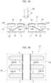
- Figures 1A, 1B ; 2A, 2B ; and 3A, 3B are pairs of cross-sectional and plan views, respectively, illustrative of processing steps according to a conventional approach intended to provide integrated circuit semiconductor (silicon, for instance) devices with wettable flanks.
- Figure 1A illustrates a portion of a leadframe reel comprising a plurality of semiconductor devices under (concurrent) processing.
- these devices comprise a substrate (leadframe) having arranged thereon one or more semiconductor chips or dice 14.
- the terms chip/s and die/dice are regarded as synonymous.
- leadframe (or “lead frame”) is currently used (see, for instance the USPC Consolidated Glossary of the United States Patent and Trademark Office) to indicate a metal frame that provides support for an integrated circuit chip or die as well as electrical leads to interconnect the integrated circuit in the die or chip (the terms chip/s and die/dice are regarded as synonymous) to other electrical components or contacts.
- a leadframe comprises an array of electrically-conductive formations (or leads, 12B for instance) that from an outline location extend inwardly in the direction of a semiconductor chip or die thus forming an array of electrically-conductive formations from a die pad (12A in Figure 1 , for instance) configured to have at least one (integrated circuit) semiconductor chip or die attached on the top/front surface thereof. This may be via conventional means such as a die attach adhesive (a die attach film or DAF, for instance).
- a die attach adhesive a die attach film or DAF, for instance
- a leadframe can be of the pre-molded type, that is a type of leadframe comprising a sculptured metal (e.g., copper) structure formed by etching a metal sheet and comprising empty spaces that are filled by an insulating compound (a resin, for instance) "pre-molded" on the sculptured metal structure.
- a sculptured metal e.g., copper
- a resin a resin, for instance
- a common substrate 12 e.g., a leadframe strip
- a common substrate 12 e.g., a leadframe strip
- leadframe strip 12 In order to concurrently process several devices, several (individual) leadframes are arranged in a leadframe strip 12 and held together via sacrificial connecting bars CB running at the periphery of the individual leadframes.
- two devices in the leadframe strip 12 are connected to the same connecting bar CB via their leads 12B. More generally, individual leadframes may be connected to the connecting bars CB both via leads 12B and/or die pads 12A. In certain cases, so-called tie bars may be provided, that is, bridge-like formations that connect the die pads (12A, for instance) or the leads (12B, for instance) of a leadframe to the connecting bars.
- devices in the leadframe strip 12 may comprise:
- the leadframe strip 12 having the chips 14 arranged thereon and provided with the insulating encapsulation of molding compound 20 may be arranged on a carrier C, as illustrated in Figures 1A to 3A , with its bottom/back surface up in order to facilitate further processing.
- Figure 1A illustrates a processing step in providing devices comprised in the leadframe reel with wettable flanks.
- connecting bars CB may be "half-etched” and are not exposed at the bottom/back surface of the leadframe reel due to the (pre-)molding compound 20' covering them.
- half-etching is a common designation in the art, which does not imply that such partial etching is by necessity to exactly half the thickness of the base sculptured structure of the leadframe.
- a first blade (or saw) B1 having a first thickness T1 is used to perform a partial cut at the connecting bars CB which removes the molding compound 20' covering the connecting bars CB. As illustrated in Figure 1B connecting bars CB are now exposed on the bottom surface of the leadframe reel.
- FIGs 2A and 2B illustrate a plating step where a layer of solderable material 18 (for instance, tin) is grown/deposited on the second (bottom) surface of the leadframe reel.
- a layer of solderable material 18 for instance, tin
- the exposed surfaces of conductive material that is, the metallic material of the leadframe
- the connecting bars CB are left uncovered during the plating step and are thus plated with a layer of solderable material 18 (tin, for instance).
- Figure 3A illustrates a final singulation step where the leadframe reel is cut into individual devices.
- a second, thinner blade B2 having a thickness (width) T2 ⁇ T1 may be used to perform a full cut of the leadframe reel resulting in the formation of wettable flanks WF on at the periphery of each individual device.
- a solderable layer 18 together with wettable flanks WF provided at the periphery of the package enhance solderability of the device to the support substrate the device is intended to be mounted (soldered) on, such as a printed circuit board (PCB) for instance.
- PCB printed circuit board
- wettable flanks WF cause the formation of a solder meniscus which facilitates automatic optical inspection of the devices soldered/mounted on the substrate.
- filaments or flakes F may form as a consequence of the action of the singulating blade B2.
- filaments/flakes F may establish electrical contact between two neighboring leads 12B, causing an undesired short circuit therebetween and consequent failure (and rejection) of the device.
- Formation of filaments F and related issues may be mitigated by frequently replacing the singulation blade B2. In fact, it is observed that filaments F are increasingly formed as the blade deteriorates.
- an insulating material is formed (coated) on the exposed (bottom) surface of the connecting bars CB to counter plating thereof.
- Solutions as described herein provide a time- and cost-effective way to reduce the possible formation of filaments F likely to short neighboring leads 12B, thus reducing the number of rejected devices.
- devices in the leadframe strip 12 as illustrated herein comprise:
- the molding compound 20 is formed on the die/leadframe -- prior -- to partial cutting indicated as B1 with the insulating material 100 coated on the second surface of the elongate sacrificial connecting bars CB exposed in response to such partial cutting.
- Figure 4 illustrates a portion of the second (back or bottom) surface of a leadframe reel after a partial cut has been performed to remove the molding compound 20 (the portion of molding compound indicated with the reference 20' in Figure 1A ) and exposing the connecting bars CB.
- a mass of insulating material 100 is formed on the second surface of the connecting bars CB that is exposed as a consequence of the removal of a portion of molding/encapsulation compound 20' (via a partial cut as illustrated in Figure 1A , for instance).
- the insulating material 100 may be formed on the connecting bars CB by any method known to those skilled in the art; possible techniques to form/coat insulating material 100 comprise, for instance:
- the insulating material 100 counters deposition of the solderable layer 18 on the connecting bars CB, thus reducing the amount of solderable material that is removed by the blade (the blade B2 illustrated in Figure 3A , for instance) in the singulations step.
- the insulating material 100 may be chosen to be a curable material in order to make it resistant to the chemicals in the plating bath.
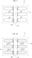
- Figures 5A and 5B are, respectively, a plan view and a perspective view of a portion of the second (bottom) surface of a leadframe reel after a plating step is performed.
- leads 12B are plated with a layer of solderable material 18 (tin, for instance) as desired, while connecting bars CB covered with a mass of insulating material 100 are not plated.
- insulating material 100 is formed at the bottom of the trench formed during the partial cut (performed via a blade B1 like the one illustrated in Figure 1A , for instance), leaving the sides of the trench exposed by the insulating material 100.
- the side surface of the leads 12B are plated with solderable material 18 thus providing wettable flanks WF to the devices in the leadframe strip 12.
- Figure 6 is illustrative of the final singulation step performed via a blade B2, for instance, where the connecting bars CB with the insulating material formed 100 thereon are removed in order to separate the leadframe strip 12 into individual devices.
- Cutting during the final singulation step thus take place along the length of the elongate sacrificial connecting bars CB that, at those locations where cutting occurs, are exempt from solder material 18 deposited at the second surface due to the presence of the insulating material 100 coated thereon.
- solderable metallic layer 18 is absent from the surface of the connecting bars CB exposed to cutting and the blade will not contact (notionally) the solderable metallic layer 18 plated on the conductive surfaces of the leadframe strip 12, thus reducing the risk of filament formation.
- the material 100 may be advantageously chosen to be:
- solutions as described herein may be advantageously applied in manufacturing processes where a plurality of integrated circuit semiconductor devices are concurrently processed.
- a plurality of semiconductor dice 14 is arranged onto a first (front) surface of a common electrically conductive substrate (such as the leadframe strip 12, for instance) that has a second surface opposite the first surface and comprises substrate portions (the individual leadframes comprising die pads 12A and leads 12B) .
- a common electrically conductive substrate such as the leadframe strip 12, for instance
- the common electrically conductive substrate comprises also elongated connecting bars CB extending between adjacent substrate portions.
- Insulating material 100 is formed on the second surface of the elongate sacrificial connecting bars CB and, subsequently, solder material 18 (tin, for instance) is grown on the second (that is, back) surface of the common electrically conductive substrate 12 having the insulating material formed on the second surface of the elongate sacrificial connecting bars (CB) .
- the insulating (and curable) material 100 counters growth of solder material 18 on the second (back) surface of the elongate sacrificial connecting bars CB thus reducing the risk of filaments formation.
- the common electrically conductive substrate 12 is finally cut (via sawing with a blade B2, for instance) along the length of the elongate sacrificial connecting bars (CB) having the insulating material (100) formed on the second surface thereof to provide finished individual devices that are notionally exempt of filaments that may cause undesired shorts (and thus rejection of the device).
- the second (back) surface of the elongate sacrificial connecting bars CB may be exposed as a consequence of a partial cut (via a blade B1 thicker than the singulating blade B2) intended to provide the package of the devices with wettable flanks.
Landscapes
- Lead Frames For Integrated Circuits (AREA)
- Engineering & Computer Science (AREA)
- Computer Hardware Design (AREA)
- Microelectronics & Electronic Packaging (AREA)
- Power Engineering (AREA)
- Physics & Mathematics (AREA)
- Condensed Matter Physics & Semiconductors (AREA)
- General Physics & Mathematics (AREA)
- Manufacturing & Machinery (AREA)
Applications Claiming Priority (1)
| Application Number | Priority Date | Filing Date | Title |
|---|---|---|---|
| IT102023000008289A IT202300008289A1 (it) | 2023-04-27 | 2023-04-27 | Procedimento per fabbricare dispositivi a semiconduttore |
Publications (2)
| Publication Number | Publication Date |
|---|---|
| EP4462467A1 true EP4462467A1 (de) | 2024-11-13 |
| EP4462467B1 EP4462467B1 (de) | 2026-02-18 |
Family
ID=87136250
Family Applications (1)
| Application Number | Title | Priority Date | Filing Date |
|---|---|---|---|
| EP24169742.4A Active EP4462467B1 (de) | 2023-04-27 | 2024-04-11 | Verfahren zur herstellung von halbleiteranordnungen |
Country Status (3)
| Country | Link |
|---|---|
| US (1) | US20240363584A1 (de) |
| EP (1) | EP4462467B1 (de) |
| IT (1) | IT202300008289A1 (de) |
Citations (8)
| Publication number | Priority date | Publication date | Assignee | Title |
|---|---|---|---|---|
| US20050116321A1 (en) * | 2002-12-10 | 2005-06-02 | National Semiconductor Corporation, A Delaware Corp. | Enhanced solder joint strength and ease of inspection of leadless leadframe package (LLP) |
| US8017447B1 (en) * | 2010-08-03 | 2011-09-13 | Linear Technology Corporation | Laser process for side plating of terminals |
| EP2680307A2 (de) | 2012-06-29 | 2014-01-01 | Freescale Semiconductor, Inc. | Halbleitervorrichtungsverpackung und Verfahren zur Herstellung |
| US20160276251A1 (en) * | 2015-03-16 | 2016-09-22 | Unisem (M) Berhad | Lead Frames With Wettable Flanks |
| EP4057342A2 (de) | 2021-03-11 | 2022-09-14 | STMicroelectronics S.r.l. | Verfahren zur herstellung von halbleiterbauelementen und entsprechendes halbleiterbauelement |
| US20220344173A1 (en) * | 2021-04-26 | 2022-10-27 | Microchip Technology Incorporated | Method of forming a surface-mount integrated circuit package with solder enhanced leadframe terminals |
| EP4099368A1 (de) | 2021-06-01 | 2022-12-07 | STMicroelectronics S.r.l. | Verfahren zur herstellung von halbleiterbauelementen und entsprechendes halbleiterbauelement |
| WO2023037682A1 (ja) * | 2021-09-08 | 2023-03-16 | Towa株式会社 | 半導体装置の製造方法およびリードフレーム |
Family Cites Families (1)
| Publication number | Priority date | Publication date | Assignee | Title |
|---|---|---|---|---|
| CN106206326B (zh) * | 2015-05-28 | 2022-05-13 | 意法半导体股份有限公司 | 用于制造表面安装类型半导体器件的方法以及对应的半导体器件 |
-
2023
- 2023-04-27 IT IT102023000008289A patent/IT202300008289A1/it unknown
-
2024
- 2024-04-11 EP EP24169742.4A patent/EP4462467B1/de active Active
- 2024-04-17 US US18/637,865 patent/US20240363584A1/en active Pending
Patent Citations (8)
| Publication number | Priority date | Publication date | Assignee | Title |
|---|---|---|---|---|
| US20050116321A1 (en) * | 2002-12-10 | 2005-06-02 | National Semiconductor Corporation, A Delaware Corp. | Enhanced solder joint strength and ease of inspection of leadless leadframe package (LLP) |
| US8017447B1 (en) * | 2010-08-03 | 2011-09-13 | Linear Technology Corporation | Laser process for side plating of terminals |
| EP2680307A2 (de) | 2012-06-29 | 2014-01-01 | Freescale Semiconductor, Inc. | Halbleitervorrichtungsverpackung und Verfahren zur Herstellung |
| US20160276251A1 (en) * | 2015-03-16 | 2016-09-22 | Unisem (M) Berhad | Lead Frames With Wettable Flanks |
| EP4057342A2 (de) | 2021-03-11 | 2022-09-14 | STMicroelectronics S.r.l. | Verfahren zur herstellung von halbleiterbauelementen und entsprechendes halbleiterbauelement |
| US20220344173A1 (en) * | 2021-04-26 | 2022-10-27 | Microchip Technology Incorporated | Method of forming a surface-mount integrated circuit package with solder enhanced leadframe terminals |
| EP4099368A1 (de) | 2021-06-01 | 2022-12-07 | STMicroelectronics S.r.l. | Verfahren zur herstellung von halbleiterbauelementen und entsprechendes halbleiterbauelement |
| WO2023037682A1 (ja) * | 2021-09-08 | 2023-03-16 | Towa株式会社 | 半導体装置の製造方法およびリードフレーム |
Non-Patent Citations (1)
| Title |
|---|
| P. SERRA ET AL.: "Laser-Induced Forward Transfer: Fundamentals and Applications", ADVANCED MATERIALS TECHNOLOGIES, vol. 4 |
Also Published As
| Publication number | Publication date |
|---|---|
| IT202300008289A1 (it) | 2024-10-27 |
| US20240363584A1 (en) | 2024-10-31 |
| EP4462467B1 (de) | 2026-02-18 |
Similar Documents
| Publication | Publication Date | Title |
|---|---|---|
| US8071426B2 (en) | Method and apparatus for no lead semiconductor package | |
| US6841414B1 (en) | Saw and etch singulation method for a chip package | |
| US10366948B2 (en) | Semiconductor device and method for manufacturing the same | |
| US8329509B2 (en) | Packaging process to create wettable lead flank during board assembly | |
| KR100275660B1 (ko) | 리드프레임, 반도체 장치의 제조방법 및 연속조립 시스템 | |
| US9363901B2 (en) | Making a plurality of integrated circuit packages | |
| CN102479767A (zh) | 具有电磁屏蔽的半导体器件封装 | |
| KR200492009Y1 (ko) | 예비성형된 리드 프레임 및 이 리드 프레임으로부터 제조된 리드 프레임 패키지 | |
| JP7473560B2 (ja) | 側壁メッキ層を有する半導体パッケージ | |
| EP3861568B1 (de) | Verpackungsverfahren zur beschichtung mit selektiven formkörpern | |
| US20020149090A1 (en) | Lead frame and semiconductor package | |
| US9287238B2 (en) | Leadless semiconductor package with optical inspection feature | |
| US20060125062A1 (en) | Semiconductor package having improved adhesion and solderability | |
| EP4462467B1 (de) | Verfahren zur herstellung von halbleiteranordnungen | |
| US20250105024A1 (en) | Method of manufacturing semiconductor devices and corresponding semiconductor device | |
| US11728179B2 (en) | Surface mount semiconductor device and method of manufacture | |
| US8969139B2 (en) | Lead frame array package with flip chip die attach | |
| US20230360928A1 (en) | Method for manufacturing semiconductor devices and corresponding semiconductor device | |
| US20240332250A1 (en) | Method of manufacturing semiconductor devices and corresponding semiconductor device | |
| US20200321228A1 (en) | Method of manufacturing a lead frame, method of manufacturing an electronic apparatus, and electronic apparatus | |
| CN118866715A (zh) | 制造半导体设备的方法 | |
| US20240178105A1 (en) | Method of manufacturing substrates for semiconductor devices, corresponding product and semiconductor device | |
| EP4489070A1 (de) | Verfahren zur herstellung von halbleiterbauelementen, entsprechender vorgeformter leiterrahmen und halbleiterbauelement | |
| US12165880B2 (en) | Method of manufacturing semiconductor devices and corresponding semiconductor device | |
| EP4542629A1 (de) | Verfahren zur herstellung von halbleiterbauelementen und zugehöriges halbleiterbauelement |
Legal Events
| Date | Code | Title | Description |
|---|---|---|---|
| PUAI | Public reference made under article 153(3) epc to a published international application that has entered the european phase |
Free format text: ORIGINAL CODE: 0009012 |
|
| STAA | Information on the status of an ep patent application or granted ep patent |
Free format text: STATUS: THE APPLICATION HAS BEEN PUBLISHED |
|
| AK | Designated contracting states |
Kind code of ref document: A1 Designated state(s): AL AT BE BG CH CY CZ DE DK EE ES FI FR GB GR HR HU IE IS IT LI LT LU LV MC ME MK MT NL NO PL PT RO RS SE SI SK SM TR |
|
| STAA | Information on the status of an ep patent application or granted ep patent |
Free format text: STATUS: REQUEST FOR EXAMINATION WAS MADE |
|
| 17P | Request for examination filed |
Effective date: 20250331 |
|
| GRAP | Despatch of communication of intention to grant a patent |
Free format text: ORIGINAL CODE: EPIDOSNIGR1 |
|
| STAA | Information on the status of an ep patent application or granted ep patent |
Free format text: STATUS: GRANT OF PATENT IS INTENDED |
|
| INTG | Intention to grant announced |
Effective date: 20250909 |
|
| GRAS | Grant fee paid |
Free format text: ORIGINAL CODE: EPIDOSNIGR3 |
|
| GRAL | Information related to payment of fee for publishing/printing deleted |
Free format text: ORIGINAL CODE: EPIDOSDIGR3 |
|
| GRAS | Grant fee paid |
Free format text: ORIGINAL CODE: EPIDOSNIGR3 |
|
| GRAA | (expected) grant |
Free format text: ORIGINAL CODE: 0009210 |
|
| STAA | Information on the status of an ep patent application or granted ep patent |
Free format text: STATUS: THE PATENT HAS BEEN GRANTED |