EP4455774A1 - Display module and display device - Google Patents
Display module and display device Download PDFInfo
- Publication number
- EP4455774A1 EP4455774A1 EP21827537.8A EP21827537A EP4455774A1 EP 4455774 A1 EP4455774 A1 EP 4455774A1 EP 21827537 A EP21827537 A EP 21827537A EP 4455774 A1 EP4455774 A1 EP 4455774A1
- Authority
- EP
- European Patent Office
- Prior art keywords
- substrate
- support plate
- electrostatic discharge
- metal
- disposed
- Prior art date
- Legal status (The legal status is an assumption and is not a legal conclusion. Google has not performed a legal analysis and makes no representation as to the accuracy of the status listed.)
- Pending
Links
Images


Classifications
-
- G—PHYSICS
- G02—OPTICS
- G02F—OPTICAL DEVICES OR ARRANGEMENTS FOR THE CONTROL OF LIGHT BY MODIFICATION OF THE OPTICAL PROPERTIES OF THE MEDIA OF THE ELEMENTS INVOLVED THEREIN; NON-LINEAR OPTICS; FREQUENCY-CHANGING OF LIGHT; OPTICAL LOGIC ELEMENTS; OPTICAL ANALOGUE/DIGITAL CONVERTERS
- G02F1/00—Devices or arrangements for the control of the intensity, colour, phase, polarisation or direction of light arriving from an independent light source, e.g. switching, gating or modulating; Non-linear optics
- G02F1/01—Devices or arrangements for the control of the intensity, colour, phase, polarisation or direction of light arriving from an independent light source, e.g. switching, gating or modulating; Non-linear optics for the control of the intensity, phase, polarisation or colour
- G02F1/13—Devices or arrangements for the control of the intensity, colour, phase, polarisation or direction of light arriving from an independent light source, e.g. switching, gating or modulating; Non-linear optics for the control of the intensity, phase, polarisation or colour based on liquid crystals, e.g. single liquid crystal display cells
- G02F1/133—Constructional arrangements; Operation of liquid crystal cells; Circuit arrangements
- G02F1/1333—Constructional arrangements; Manufacturing methods
- G02F1/133308—Support structures for LCD panels, e.g. frames or bezels
- G02F1/133314—Back frames
-
- G—PHYSICS
- G02—OPTICS
- G02F—OPTICAL DEVICES OR ARRANGEMENTS FOR THE CONTROL OF LIGHT BY MODIFICATION OF THE OPTICAL PROPERTIES OF THE MEDIA OF THE ELEMENTS INVOLVED THEREIN; NON-LINEAR OPTICS; FREQUENCY-CHANGING OF LIGHT; OPTICAL LOGIC ELEMENTS; OPTICAL ANALOGUE/DIGITAL CONVERTERS
- G02F1/00—Devices or arrangements for the control of the intensity, colour, phase, polarisation or direction of light arriving from an independent light source, e.g. switching, gating or modulating; Non-linear optics
- G02F1/01—Devices or arrangements for the control of the intensity, colour, phase, polarisation or direction of light arriving from an independent light source, e.g. switching, gating or modulating; Non-linear optics for the control of the intensity, phase, polarisation or colour
- G02F1/13—Devices or arrangements for the control of the intensity, colour, phase, polarisation or direction of light arriving from an independent light source, e.g. switching, gating or modulating; Non-linear optics for the control of the intensity, phase, polarisation or colour based on liquid crystals, e.g. single liquid crystal display cells
- G02F1/133—Constructional arrangements; Operation of liquid crystal cells; Circuit arrangements
- G02F1/136—Liquid crystal cells structurally associated with a semi-conducting layer or substrate, e.g. cells forming part of an integrated circuit
- G02F1/1362—Active matrix addressed cells
- G02F1/1368—Active matrix addressed cells in which the switching element is a three-electrode device
-
- G—PHYSICS
- G02—OPTICS
- G02F—OPTICAL DEVICES OR ARRANGEMENTS FOR THE CONTROL OF LIGHT BY MODIFICATION OF THE OPTICAL PROPERTIES OF THE MEDIA OF THE ELEMENTS INVOLVED THEREIN; NON-LINEAR OPTICS; FREQUENCY-CHANGING OF LIGHT; OPTICAL LOGIC ELEMENTS; OPTICAL ANALOGUE/DIGITAL CONVERTERS
- G02F1/00—Devices or arrangements for the control of the intensity, colour, phase, polarisation or direction of light arriving from an independent light source, e.g. switching, gating or modulating; Non-linear optics
- G02F1/01—Devices or arrangements for the control of the intensity, colour, phase, polarisation or direction of light arriving from an independent light source, e.g. switching, gating or modulating; Non-linear optics for the control of the intensity, phase, polarisation or colour
- G02F1/13—Devices or arrangements for the control of the intensity, colour, phase, polarisation or direction of light arriving from an independent light source, e.g. switching, gating or modulating; Non-linear optics for the control of the intensity, phase, polarisation or colour based on liquid crystals, e.g. single liquid crystal display cells
- G02F1/133—Constructional arrangements; Operation of liquid crystal cells; Circuit arrangements
- G02F1/1333—Constructional arrangements; Manufacturing methods
- G02F1/1345—Conductors connecting electrodes to cell terminals
- G02F1/13452—Conductors connecting driver circuitry and terminals of panels
-
- G—PHYSICS
- G02—OPTICS
- G02F—OPTICAL DEVICES OR ARRANGEMENTS FOR THE CONTROL OF LIGHT BY MODIFICATION OF THE OPTICAL PROPERTIES OF THE MEDIA OF THE ELEMENTS INVOLVED THEREIN; NON-LINEAR OPTICS; FREQUENCY-CHANGING OF LIGHT; OPTICAL LOGIC ELEMENTS; OPTICAL ANALOGUE/DIGITAL CONVERTERS
- G02F1/00—Devices or arrangements for the control of the intensity, colour, phase, polarisation or direction of light arriving from an independent light source, e.g. switching, gating or modulating; Non-linear optics
- G02F1/01—Devices or arrangements for the control of the intensity, colour, phase, polarisation or direction of light arriving from an independent light source, e.g. switching, gating or modulating; Non-linear optics for the control of the intensity, phase, polarisation or colour
- G02F1/13—Devices or arrangements for the control of the intensity, colour, phase, polarisation or direction of light arriving from an independent light source, e.g. switching, gating or modulating; Non-linear optics for the control of the intensity, phase, polarisation or colour based on liquid crystals, e.g. single liquid crystal display cells
- G02F1/133—Constructional arrangements; Operation of liquid crystal cells; Circuit arrangements
- G02F1/136—Liquid crystal cells structurally associated with a semi-conducting layer or substrate, e.g. cells forming part of an integrated circuit
- G02F1/1362—Active matrix addressed cells
- G02F1/136204—Arrangements to prevent high voltage or static electricity failures
-
- G—PHYSICS
- G02—OPTICS
- G02F—OPTICAL DEVICES OR ARRANGEMENTS FOR THE CONTROL OF LIGHT BY MODIFICATION OF THE OPTICAL PROPERTIES OF THE MEDIA OF THE ELEMENTS INVOLVED THEREIN; NON-LINEAR OPTICS; FREQUENCY-CHANGING OF LIGHT; OPTICAL LOGIC ELEMENTS; OPTICAL ANALOGUE/DIGITAL CONVERTERS
- G02F2202/00—Materials and properties
- G02F2202/22—Antistatic materials or arrangements
Definitions
- the present invention relates to a field of display technology, and in particular to a display module and a display device.
- vehicle display modules mainly include a frame body 1, a panel body 2 and a fixed cover 3, fixed cover 3 is connected to the frame body 1 through the fixing tape 9 to form a closed space 400, the panel main body 2 is integrally disposed in the closed space 400 and is connected to the fixed cover 3 by adhesive 8.
- the panel main body 2 includes a laminated first polarizing structure 4, an array substrate 5, a color filter substrate 6 and a laminated second polarizing structure 7.
- the panel body 2 is bonded to the fixed cover 3 on the side where the second polarizing structure 7 is provided.
- This structure using adhesive 8 to connect the fixed cover plate 3 and the panel body 2 is easy to lead to excessive thickness of the vehicle display module, which is not suitable for the development demand of thinning the vehicle display module.
- the present invention provides display module and a display device to solve the technical problem of large thickness of vehicle display module.
- the present invention provides a display module including a metal back frame and a display panel disposed on the metal back frame, wherein the display panel includes:
- the display panel further includes an opposing area and a connecting area surrounding the opposing area;
- the display module further includes a first conductive adhesive located in the connecting area and connecting the first substrate with the metal back frame; and the thin film transistor layer includes a first electrostatic discharge terminal located in the connecting area, and the first conductive adhesive is electrically connecing the metal support platewith the first electrostatic discharge terminal.
- the thin film transistor layer is provided with a first groove located in the connecting area, and the first electrostatic discharge terminal is disposed in the first groove; and one end of the first conductive adhesive is electrically connected to the metal support plate, and another end of the first conductive adhesive is disposed in the first groove and is electrically connected to the first electrostatic discharge terminal.
- the thin film transistor layer further includes a first metal layer disposed on the substrate, a second metal layer disposed on the first metal layer, and an insulating layer stacked with the first metal layer and the second metal layer, and the first groove is defined inthe insulating layer and located in the connecting area; and the first metal layer includes the first electrostatic discharge terminal, or the second metal layer includes the first electrostatic discharge terminal.
- the second metal layer includes the first electrostatic discharge terminal
- the insulating layer includes a first insulating sublayer disposed on a side of the second metal layer away from the substrate; and the first groove corresponds to the first electrostatic discharge terminal and is defined indefined in the first insulating sublayer.
- the first metal layer includes the first electrostatic discharge terminal
- the insulating layer includes a first insulating sublayer disposed on one side of the second metal layer away from the substrate, and a second insulating sublayer disposed between the first metal layer and the second metal layer; and the first groove corresponds to the first electrostatic discharge terminal and is defined in the first insulating sublayer and the second insulating sublayer.
- the metal support plate is provided with a second groove located in the connecting area; and one end of the first conductive adhesive is disposed in the second groove and is electrically connected to the metal support plate, and another end of the first conductive adhesive is disposed in the first groove and is electrically connected to the first electrostatic discharge terminal.
- the second groove is annularly defined in the metal support plate and disposed around the opposing area.
- an orthograph projection of the first conductive adhesive on the substrate overlaps an orthograph projection of the first electrostatic discharge terminal on the substrate.
- the first connecting part is disposed around the display driving part and connected to the metal support plate, and the second substrate is disposed opposite to the display driving part and is located in the opposing area.
- the connecting area includes a first connecting subarea and a second connecting subarea
- the metal support plate includes a first support plate located in the first connecting subarea and a second support plate located in the second connecting subarea, and a distance from the second support plate to the first substrate is greater than a distance from the first support plate to the first substrate
- the second substrate includes a second connecting part located in the second connecting subarea, the first support plate and the first connecting part are connected in the first connecting subarea, and the second support plate and the second connecting part are connected in the second connecting subarea.
- the display module further includes a first conductive adhesive located in the first connecting subarea and connecting the first connecting part with the first support plate, and a second conductive adhesive located in the second connecting subarea and connecting the second connecting part with the second support plate; and the first substrate further includes a first electrostatic discharge terminal located in the first connecting subarea, the second substrate further includes a second electrostatic discharge terminal located in the second connecting subarea, the first conductive adhesive is electrically connected the first support plate with the first electrostatic discharge terminal, and the second conductive adhesive is electrically connected the second support plate with the second electrostatic discharge terminal.
- the present invention further provides a display device including a display module and a device main body, wherein the display module and the device main body are combined into one body.
- the display panel further includes an opposing area and a connecting area surrounding the opposing area;
- the display module further includes a first conductive adhesive located in the connecting area and connectingthe first substrate with the metal back frame; and the thin film transistor layer includes a first electrostatic discharge terminal located in the connecting area, and the first conductive adhesive is electrically connected the metal support plate with the first electrostatic discharge terminal.
- the thin film transistor layer is provided with a first groove located in the connecting area, and the first electrostatic discharge terminal is disposed in the first groove; and one end of the first conductive adhesive is electrically connected to the metal support plate, and another end of the first conductive adhesive is disposed in the first groove and is electrically connected to the first electrostatic discharge terminal.
- the thin film transistor layer further includes a first metal layer disposed on the substrate, a second metal layer disposed on the first metal layer, and an insulating layer stacked with the first metal layer and the second metal layer, and the first groove is defined in the insulating layer and located in the connecting area; and the first metal layer includes the first electrostatic discharge terminal, or the second metal layer includes the first electrostatic discharge terminal.
- the connecting area includes a first connecting subarea and a second connecting subarea
- the metal support plate includes a first support plate located in the first connecting subarea and a second support plate located in the second connecting subarea, and a distance from the second support plate to the first substrate is greater than a distance from the first support plate to the first substrate
- the second substrate includes a second connecting part located in the second connecting subarea, the first support plate and the first connecting part are connected in the first connecting subarea, and the second support plate and the second connecting part are connected in the second connecting subarea.
- the display module further includes a first conductive adhesive located in the first connecting subarea and connecting the first connecting part with the first support plate, and a second conductive adhesive located in the second connecting subarea and connecting the second connecting part with the second support plate; and the first substrate further includes a first electrostatic discharge terminal located in the first connecting subarea, the second substrate further includes a second electrostatic discharge terminal located in the second connecting subarea, the first conductive adhesive is electrically connected the first support plate with the first electrostatic discharge terminal, and the second conductive adhesive is electrically connected the second support plate with the second electrostatic discharge terminal.
- the beneficial effect of the application by disposing the first substrate of the display panel on the metal back frame, and disposing the second substrate of the display panel opposite to the first substrate and located between the first substrate and the metal back frame, the complexity of the overall structure of the display module is reduced. Obviously, this structure that the first substrate of the display panel directly disposes on the metal back frame omits the adhesive, the fixed cover plate, and other original related films, and the thickness of the display module is reduced to meet the thinning requirements of the display module.
- first and second are only used for descriptive purposes and cannot be understood as indicating or implying relative importance or implicitly indicating the number of indicated technical features. Thus, the features defining “first” and “second” may explicitly or implicitly include one or more of the features. In the description of this application, “multiple” means two or more, unless otherwise expressly and specifically defined.
- connection should be understood in a broad sense, for example, it can be fixed connection, removable connection, or integrated connection; it can be mechanical connection, electrical connection or mutual communication; it can be directly connected or indirectly connected through an intermediate medium, it can be the connection within two elements or the interaction relationship between two elements.
- connection should be understood in a broad sense, for example, it can be fixed connection, removable connection, or integrated connection; it can be mechanical connection, electrical connection or mutual communication; it can be directly connected or indirectly connected through an intermediate medium, it can be the connection within two elements or the interaction relationship between two elements.
- the embodiment of the present application provides a display module including a metal back frame 10 and a display panel 20 disposed on the metal back frame 10, wherein the display panel includes:
- vehicle display modules mainly include a frame body 1, a panel body 2 and a fixed cover 3, fixed cover 3 is connected to the frame body 1 through the fixing tape 9 to form a closed space 400, the panel main body 2 is integrally disposed in the closed space 400 and is connected to the fixed cover 3 by adhesive 8.
- the panel main body 2 includes a laminated first polarizing structure 4, an array substrate 5, a color filter substrate 6 and a laminated second polarizing structure 7.
- the panel body 2 is bonded to the fixed cover 3 on the side where the second polarizing structure 7 is provided.
- This structure using adhesive 8 to connect the fixed cover plate 3 and the panel body 2 is easy to lead to excessive thickness of the vehicle display module, which is not suitable for the development demand of thinning the vehicle display module;
- the first substrate 21 of the display panel 20 on the metal back frame 10
- the second substrate 22 of the display panel 20 opposite the first substrate 21 and located between the first substrate 21 and the metal back frame 10
- the complexity of the overall structure of the display module is reduced.
- this structure of that the first substrate 21 of the display panel directly disposes on the metal back frame 10 omits the adhesive 8, the fixed cover plate 3 and other related original films, and the thickness of the display module is reduced, to meet the thinning requirements of the display module.
- the vehicle display module is assembled through the connection between the fixed cover plate 3 and the frame 1 and he connection between the fixed cover plate 3 and the panel body 2 respectively.
- the structure in which the fixed cover plate 3 and the panel body 2 are bonded and fixed by adhesive 8 is also easy to increase the difficulty of the vehicle display module process.
- the first substrate 21 includes a substrate 211 and a thin film transistor layer 212 disposed on the side of the substrate 211 close to the second substrate 22.
- the substrate 211 is a hard substrate to protect other functional films in the display module., specifically, the substrate 211 can be a glass substrate.
- the display panel 20 further includes a first polarizer 24 and a second polarizer 25.
- the first polarizer 24 is disposed on the side of the first substrate 21 away from the second substrate 22, and the second polarizer 25 is disposed on the side of the second substrate 22 away from the first substrate 21.
- the display module further includes a backlight module 26 disposed between the display panel 20 and the metal back frame 10 and located in a holding space 100, the backlight module 26 at least includes a stacked reflector 261, a light guide plate 262 and an optical film 263.
- the backlight module 26 is a side entry structure or a straight down structure, which is not limited here.
- the display panel further includes an opposing area 200 and a connecting area 300 surrounding the opposing area 200;
- the display panel 20 includes an opposing area 200 and a connecting area 300 surrounding the opposing area 200, and divides the first substrate 21 into a display driving unit 213 located in the opposing area 200 and a first connection part 214 located in the connecting area 300, and the metal back frame 10 is divided into a metal back cover 11 disposed opposite to the first substrate 21 and a metal support plate 12 extending from the peripheral side of the metal back cover 11 to the direction of the first substrate 21.
- the metal support plate 12 is located in the connecting area 300 and connected to the first connection part 214, to realize the connection between the first substrate 21 and the metal back frame 10 in the connecting area 300.
- the first connecting part 214 can be disposed around the display driving part 213 and connected to the metal support plate 12, the second substrate 22 can be disposed opposite to the display driving part 213 and located in the opposing area 200, and the first substrate 21, the metal back cover 11 and the metal support plate 12 can be enclosed to form a holding space 100.
- the second substrate 22 can be located in the holding space, the second substrate 22 can be disposed opposite to the display driving unit 213 and located in the opposing area 200, that is, the second substrate 22 is aligned with the display driving unit 213, and the liquid crystal layer 23 is disposed between the second substrate 22 and the display driving part 213, to realize the function of driving the liquid crystal deflection in the liquid crystal layer 23.
- the display module further includes a first conductive adhesive 30 located in the connecting area 300 and connecting the first substrate 21 with the metal back frame 10; and the thin film transistor layer 212 includes a first electrostatic discharge terminal 2120 located in the connecting area 300, and the first conductive adhesive 30 is electrically connecing the metal support plate 12 with the first electrostatic discharge terminal 2120.
- the vehicle display module is assembled through the connection of the fixed cover plate 3 with the frame 1 and the panel body 2 respectively, wherein the fixed cover plate 3 is connected to the panel body 2 through the adhesive 8, and the fixed cover plate 3 is connected to the frame 1 through the fixed adhesive 9, so that the static electricity generated on the panel body 2 cannot be released to the frame 1, the electrostatic discharge capacity of the vehicle display module is low, which affects the use experience.
- the display module includes a first conductive adhesive 30 located in the connecting area 300 and connecting the first substrate 21 with the metal back frame 10, and the thin film transistor layer 212 includes a first electrostatic discharge terminal 2120 located in the connecting area 300, which electrically connected the metal support plate 12 to the first electrostatic discharge terminal 2120 through the first conductive adhesive 30.
- the first conductive adhesive 30 may be a conductive foam tape or an optical adhesive embedded with conductive gold balls.
- thin film transistor layer 212 is provided with a first groove 2121 located in the connecting area 300, and the first electrostatic discharge terminal 2120 is disposed in the first groove 2121; and one end of the first conductive adhesive 30 is electrically connected to the metal support plate 12, and another end of the first conductive adhesive 30 is disposed in the first groove 2121 and is electrically connected to the first electrostatic discharge terminal 2120.
- the thin film transistor layer 212 includes a first groove 2121 located in the connecting area 300, and the first electrostatic discharge terminal 2120 is disposed in the first groove 2121, and one end of the first conductive adhesive 30 is electrically connected to the metal support plate 12, another end of the first conductive adhesive 30 is disposed in the first groove 2121 and electrically connected to the first electrostatic discharge terminal 2120.
- first conductive adhesive 30 By setting the first groove 2121, one end of the first conductive adhesive 30 is disposed in the first groove 2121 and electrically connected to the first electrostatic discharge terminal 2120, the first conductive adhesive 30 is prevented from being squeezed between the first panel and the metal back frame 10, which further reduces the thickness of the display module, and also ensures the full contact between the first conductive adhesive 30 and the first electrostatic discharge terminal 2120.
- the thin film transistor layer 212 further includes a first metal layer 2122 disposed on the substrate 211, a second metal layer 2123 disposed on the first metal layer 2122, and an insulating layer stacked with the first metal layer 2122 and the second metal layer 2123, and the first groove 2121 is defined in the insulating layer and located in the connecting area 300; and the first metal layer 2122 includes the first electrostatic discharge terminal 2120, or the second metal layer 2123 includes the first electrostatic discharge terminal 2120.
- the thin film transistor layer 212 includes a first metal layer 2122 disposed on the substrate 211, a second metal layer 2123 disposed on the first metal layer 2122, and an insulating layer stacked with the first metal layer 2122 and the second metal layer 2123, the first groove 2121 is disposed on the insulating layer and located in the connecting area 300.
- the first metal layer 2122 includes the first electrostatic discharge terminal 2120, or the second metal layer 2123 includes the first electrostatic discharge terminal 2120, that is, the first metal layer 2122 and the first electrostatic discharge terminal 2120 are disposed on the same layer, or the second metal layer 2123 and the first electrostatic discharge terminal 2120 are disposed on the same layer.
- the static electricity on the thin film transistor layer 212 can be released to the metal back frame 10 without adding a new film layer structure.
- the first metal layer 2122 can further include a gate located in the opposing area 200
- the second metal layer 2123 can further include a source and a drain located in the opposing area 200.
- the second metal layer 2123 includes the first electrostatic discharge terminal 2120
- the insulating layer includes a first insulating sublayer 2124 disposed on a side of the second metal layer 2123 away from the substrate 211; and the first groove 2121 corresponds to the first electrostatic discharge terminal 2120 and is defined in the first insulating sublayer 2124.
- the second metal layer 2123 includes the first electrostatic discharge terminal 2120, that is, the second metal layer 2123 and the first electrostatic discharge terminal 2120 are disposed on the same layer, and the insulating layer includes the first insulator layer 2124 disposed on the side of the second metal layer 2123 away from the substrate 211.
- the first groove 2121 corresponds to the first electrostatic discharge terminal 2120 and is defined in the first insulator layer 2124, so that the first conductive adhesive 30 can be electrically connected to the first electrostatic discharge terminal 2120 through the first groove 2121.
- the first metal layer 2122 includes the first electrostatic discharge terminal 2120
- the insulating layer includes a first insulating sublayer 2124 disposed on one side of the second metal layer 2123 away from the substrate 211, and a second insulating sublayer 2125 disposed between the first metal layer 2122 and the second metal layer 2123; and the first groove 2121 corresponds to the first electrostatic discharge terminal 2120 and is defined in the first insulating sublayer 2124 and the second insulating sublayer 2125.
- the first metal layer 2122 includes the first electrostatic discharge terminal 2120, that is, the first metal layer 2122 and the first electrostatic discharge terminal 2120 are disposed on the same layer, and the insulating layer includes the first insulator layer 2124 disposed on the side of the second metal layer 2123 away from the substrate 211.
- a second insulator layer 2125 disposed between the first metal layer 2122 and the second metal layer 2123, the first groove 2121 corresponds to the first electrostatic discharge terminal 2120 and is defined in the first insulator layer 2124 and the second insulator layer 2125 so that the first groove 2121 passes through the first insulator layer 2124 and the second insulator layer 2125.
- the depth of the first groove 2121 is maximized, so that the volume containing the first conductive adhesive 30 is increased, compared with the structure disposed on the same layer of the second metal layer 2123 and the first electrostatic discharge terminal 2120, the thickness of the display module is further reduced.
- the metal support plate 12 is provided with a second groove 121 located in the connecting area 300; and one end of the first conductive adhesive 30 is disposed in the second groove 121 and is electrically connected to the metal support plate 12, and another end of the first conductive adhesive 30 is disposed in the first groove 2121 and is electrically connected to the first electrostatic discharge terminal 2120.
- the metal support plate 12 is provided with a second groove 121 located in the connecting area 300
- the thin film transistor layer 212 is provided with a first groove 2121 located in the connecting area 300, so that one end of the first conductive adhesive 30 is disposed in the second groove 121 and electrically connected to the metal support plate 12, another end of the first conductive adhesive 30 is disposed in the first groove 2121 and electrically connected to the first electrostatic discharge terminal 2120, so that both ends of the first conductive adhesive 30 are disposed in the first groove 2121 and the second groove 121 as much as possible, reducing the thickness of the display module, the electrostatic discharge on the thin film transistor layer 212 to the metal back frame 10 is also realized.
- the second groove 121 is annularly defined in the metal support plate 12 and disposed around the opposing area 200. It can be understood that the second groove 121 is a ring and annularly disposed around the opposing area 200, and the first conductive adhesive 30 is at least disposed in the second groove 121, so as to facilitate the bonding of the first substrate 21 and the metal back frame 10 through the first conductive adhesive 30, and increase the area of electrical connection between the metal back frame 10 and the first conductive adhesive 30 at the same time, it is convenient to discharge static electricity on the thin film transistor layer 212 to the metal back frame 10.
- an orthograph projection of the first conductive adhesive 30 on the substrate 211 overlaps an orthograph projection of the first electrostatic discharge terminal 2120 on the substrate 211.
- the orthograph projection of the first conductive adhesive 30 on the substrate 211 overlaps the orthograph projection of the first electrostatic discharge terminal 2120 on the substrate 211, that is, the first conductive adhesive 30 is completely covered on the first electrostatic discharge terminal 2120, so that the first conductive adhesive 30 is fully electrically connected to the first electrostatic discharge terminal 2120, it is convenient to discharge static electricity on the thin film transistor layer 212 to the metal back frame 10.
- the first conductive adhesive 30 is completely covered on the first electrostatic discharge terminal 2120, so that the first conductive adhesive 30 is fully electrically connected to the first electrostatic discharge terminal 2120, it is convenient to discharge static electricity on the thin film transistor layer 212 to the metal back frame 10.
- the connecting area 300 includes a first connecting subarea 310 and a second connecting subarea 320
- the metal support plate 12 includes a first support plate 121 located in the first connecting subarea 310 and a second support plate 122 located in the second connecting subarea 320, and a distance from the second support plate 122 to the first substrate 21 is greater than a distance from the first support plate 121 to the first substrate 21
- the second substrate 22 includes a second connecting part 221 located in the second connecting subarea 320, the first support plate 121 and the first connecting part 214 are connected in the first connecting subarea 310, and the second support plate 122 and the second connecting part 221 are connected in the second connecting subarea 320.
- the connecting area 300 includes a first connecting subarea 310 and a second connecting subarea 320
- the metal support plate 12 includes a first support plate 121 located in the first connecting subarea 310 and a second support plate 122 located in the second connecting subarea 320
- the spacing between the second support plate 122 and the first substrate 21 is set to be greater than the spacing between the first support plate 121 and the first substrate 21, so that the first substrate 21 extends into the second connecting subarea 320, so that the metal support plate 12 can be connected to the first substrate 21 in the first connecting subarea 310.
- the metal support plate 12 is connected to the second substrate 22 in the second connecting subarea 320, specifically, the second substrate 22 includes a second connecting part 221 located in the second connecting subarea 320, and the first support plate 121 and the first connecting part 214 are connected in the first connecting subarea 310, the second support plate 122 and the second connecting part 221 are connected in the second connecting subarea 320, thereby reducing the thickness of the display module to meet the thinning requirements of the display module.
- the display module further includes a first conductive adhesive 30 located in the first connecting subarea 310 and connecting the first connecting part 214 with he first support plate 121, and a second conductive adhesive 40 located in the second connecting subarea 320 and connecting the second connecting part 221 with the second support plate 122; and the first substrate 21 further includes a first electrostatic discharge terminal 2120 located in the first connecting subarea 310, the second substrate 22 further includes a second electrostatic discharge terminal 2200 located in the second connecting subarea 320, the first conductive adhesive 30 is electrically connected the first support plate 121 with the first electrostatic discharge terminal 2120, and the second conductive adhesive 40 is electrically connected the second support plate 122 with the second electrostatic discharge terminal 2200.
- the vehicle display module is assembled with the frame 1 and the panel body 2 respectively through the connection of the fixed cover plate 3, wherein the fixed cover plate 3 is connected with the panel body 2 through the adhesive 8. And the fixed cover plate 3 is connected with the frame 1 through the fixed adhesive 9, so that the static electricity generated on the panel body 2 cannot be released to the frame 1.
- the electrostatic discharge capacity of the vehicle display module is low, which affects the use experience.
- the display module includes a first conductive adhesive 30 located in the first connecting subarea 310 and connecting the first connecting part 214 with the first support plate 121, and a second conductive adhesive 40 located in the second connecting subarea 320 and connecting the second connecting part 221 with the second support plate 122, and the first substrate 21 further includes a first electrostatic discharge terminal 2120 located in the first connecting subarea 310.
- the second substrate 22 includes a second electrostatic discharge terminal 2200 located in the second connecting subarea 320, and the first conductive adhesive 30 is electrically connected the first support plate 121 with the first electrostatic discharge terminal 2120, the second conductive adhesive 40 electrically connected the second support plate 122 with the second electrostatic discharge terminal 2200, and electrically connected the first support plate 121 with the first electrostatic discharge terminal 2120 through the first conductive adhesive 30, so as to facilitate the electrostatic discharge on the first substrate 21 to the metal back frame 10, the second support plate 122 and the second electrostatic discharge terminal 2200 are electrically connected through the second conductive adhesive 40, so as to facilitate the electrostatic discharge on the second substrate 22 to the metal back frame, and improve the electrostatic discharge capacity of the display module.
- the first conductive adhesive 30 and the second conductive adhesive 40 may be conductive foam tape or optical adhesive embedded with conductive golden balls.
- the orthograph projection of the second conductive adhesive 40 on the first substrate 21 can overlaps the orthograph projection of the second electrostatic discharge terminal 2200 on the first substrate 21, and the second electrostatic discharge terminal 2200 can be electrically connected to the metal layer in the second substrate 22.
- the specific connection structure is not limited here.
- the embodiment of the application further provides a display device, which includes the display module and the device body as in the previous embodiment, and the display module and the device main body are combined into one body.
- the present application reduces the complexity of the overall structure of the display module by setting the first substrate 21 of the display panel 20 on the metal back frame 10, and setting the second substrate 22 of the display panel 20 opposite to the first substrate 21 and located between the first substrate 21 and the metal back frame 10. Obviously, this structure of directly setting the first substrate 21 of the display panel 20 on the metal back frame 10, the original film layers such as adhesive 8 and fixed cover plate 3 are omitted, and the thickness of the display module is reduced to meet the thinning requirements of the display module.
Landscapes
- Physics & Mathematics (AREA)
- Nonlinear Science (AREA)
- Mathematical Physics (AREA)
- Chemical & Material Sciences (AREA)
- Crystallography & Structural Chemistry (AREA)
- General Physics & Mathematics (AREA)
- Optics & Photonics (AREA)
- Engineering & Computer Science (AREA)
- Microelectronics & Electronic Packaging (AREA)
- Devices For Indicating Variable Information By Combining Individual Elements (AREA)
- Liquid Crystal (AREA)
Abstract
Description
- The present invention relates to a field of display technology, and in particular to a display module and a display device.
- With the development of display technology and automotive technology, vehicle display modules have received widespread attention. At present, as shown in
FIG. 1 , vehicle display modules mainly include aframe body 1, apanel body 2 and a fixed cover 3, fixed cover 3 is connected to theframe body 1 through thefixing tape 9 to form a closedspace 400, the panelmain body 2 is integrally disposed in the closedspace 400 and is connected to the fixed cover 3 by adhesive 8. The panelmain body 2 includes a laminated first polarizingstructure 4, anarray substrate 5, acolor filter substrate 6 and a laminated second polarizingstructure 7. Thepanel body 2 is bonded to the fixed cover 3 on the side where the second polarizingstructure 7 is provided. Thisstructure using adhesive 8 to connect the fixed cover plate 3 and thepanel body 2 is easy to lead to excessive thickness of the vehicle display module, which is not suitable for the development demand of thinning the vehicle display module. - The present invention provides display module and a display device to solve the technical problem of large thickness of vehicle display module.
- The present invention provides a display module including a metal back frame and a display panel disposed on the metal back frame, wherein the display panel includes:
- a first substrate, wherein at least one end of the first substrate is disposed on the metal back frame; and
- a second substrate disposed opposite to the first substrate and located between the first substrate and the metal back frame, wherein a liquid crystal layer is disposed between the first substrate and the second substrate; and
- wherein the first substrate includes a base and a thin film transistor layer disposed on one side of the base close to the second substrate.
- In some embodiment of the display module, the display panel further includes an opposing area and a connecting area surrounding the opposing area;
- the first substrate further includes a display driving part located in the opposing area and a first connecting part located in the connecting area; and
- the metal back frame includes a metal back cover disposed opposite to the first substrate and a metal support plate extending along a direction from the peripheral side of the metal back cover to the first substrate, and the metal support plate is located in the connecting area and connected to the first connecting part.
- In some embodiment of the display module, the display module further includes a first conductive adhesive located in the connecting area and connecting the first substrate with the metal back frame; and
the thin film transistor layer includes a first electrostatic discharge terminal located in the connecting area, and the first conductive adhesive is electrically connecing the metal support platewith the first electrostatic discharge terminal. - In some embodiment of the display module, the thin film transistor layer is provided with a first groove located in the connecting area, and the first electrostatic discharge terminal is disposed in the first groove; and
one end of the first conductive adhesive is electrically connected to the metal support plate, and another end of the first conductive adhesive is disposed in the first groove and is electrically connected to the first electrostatic discharge terminal. - In some embodiment of the display module, the thin film transistor layer further includes a first metal layer disposed on the substrate, a second metal layer disposed on the first metal layer, and an insulating layer stacked with the first metal layer and the second metal layer, and the first groove is defined inthe insulating layer and located in the connecting area; and
the first metal layer includes the first electrostatic discharge terminal, or the second metal layer includes the first electrostatic discharge terminal. - In some embodiment of the display module, the second metal layer includes the first electrostatic discharge terminal, and the insulating layer includes a first insulating sublayer disposed on a side of the second metal layer away from the substrate; and
the first groove corresponds to the first electrostatic discharge terminal and is defined indefined in the first insulating sublayer. - In some embodiment of the display module, the first metal layer includes the first electrostatic discharge terminal, and the insulating layer includes a first insulating sublayer disposed on one side of the second metal layer away from the substrate, and a second insulating sublayer disposed between the first metal layer and the second metal layer; and
the first groove corresponds to the first electrostatic discharge terminal and is defined in the first insulating sublayer and the second insulating sublayer. - In some embodiment of the display module, the metal support plate is provided with a second groove located in the connecting area; and
one end of the first conductive adhesive is disposed in the second groove and is electrically connected to the metal support plate, and another end of the first conductive adhesive is disposed in the first groove and is electrically connected to the first electrostatic discharge terminal. - In some embodiment of the display module, the second groove is annularly defined in the metal support plate and disposed around the opposing area.
- In some embodiment of the display module, an orthograph projection of the first conductive adhesive on the substrate overlaps an orthograph projection of the first electrostatic discharge terminal on the substrate.
- In some embodiment of the display module, the first connecting part is disposed around the display driving part and connected to the metal support plate, and the second substrate is disposed opposite to the display driving part and is located in the opposing area.
- In some embodiment of the display module, the connecting area includes a first connecting subarea and a second connecting subarea, the metal support plate includes a first support plate located in the first connecting subarea and a second support plate located in the second connecting subarea, and a distance from the second support plate to the first substrate is greater than a distance from the first support plate to the first substrate; and
the second substrate includes a second connecting part located in the second connecting subarea, the first support plate and the first connecting part are connected in the first connecting subarea, and the second support plate and the second connecting part are connected in the second connecting subarea. - In some embodiment of the display module, the display module further includes a first conductive adhesive located in the first connecting subarea and connecting the first connecting part with the first support plate, and a second conductive adhesive located in the second connecting subarea and connecting the second connecting part with the second support plate; and
the first substrate further includes a first electrostatic discharge terminal located in the first connecting subarea, the second substrate further includes a second electrostatic discharge terminal located in the second connecting subarea, the first conductive adhesive is electrically connected the first support plate with the first electrostatic discharge terminal, and the second conductive adhesive is electrically connected the second support plate with the second electrostatic discharge terminal. - The present invention further provides a display device including a display module and a device main body, wherein the display module and the device main body are combined into one body.
- In some embodiment of the display device, the display panel further includes an opposing area and a connecting area surrounding the opposing area;
- the first substrate further includes a display driving part located in the opposing area and a first connecting part located in the connecting area; and
- the metal back frame includes a metal back cover disposed opposite to the first substrate and a metal support plate extending along a direction from the peripheral side of the metal back cover to the first substrate, and the metal support plate is located in the connecting area and connected to the first connecting part.
- In some embodiment of the display device, the display module further includes a first conductive adhesive located in the connecting area and connectingthe first substrate with the metal back frame; and
the thin film transistor layer includes a first electrostatic discharge terminal located in the connecting area, and the first conductive adhesive is electrically connected the metal support plate with the first electrostatic discharge terminal. - In some embodiment of the display device, wherein the thin film transistor layer is provided with a first groove located in the connecting area, and the first electrostatic discharge terminal is disposed in the first groove; and
one end of the first conductive adhesive is electrically connected to the metal support plate, and another end of the first conductive adhesive is disposed in the first groove and is electrically connected to the first electrostatic discharge terminal. - In some embodiment of the display device, the thin film transistor layer further includes a first metal layer disposed on the substrate, a second metal layer disposed on the first metal layer, and an insulating layer stacked with the first metal layer and the second metal layer, and the first groove is defined in the insulating layer and located in the connecting area; and
the first metal layer includes the first electrostatic discharge terminal, or the second metal layer includes the first electrostatic discharge terminal. - In some embodiment of the display device, the connecting area includes a first connecting subarea and a second connecting subarea, the metal support plate includes a first support plate located in the first connecting subarea and a second support plate located in the second connecting subarea, and a distance from the second support plate to the first substrate is greater than a distance from the first support plate to the first substrate; and
the second substrate includes a second connecting part located in the second connecting subarea, the first support plate and the first connecting part are connected in the first connecting subarea, and the second support plate and the second connecting part are connected in the second connecting subarea. - In some embodiment of the display device, the display module further includes a first conductive adhesive located in the first connecting subarea and connecting the first connecting part with the first support plate, and a second conductive adhesive located in the second connecting subarea and connecting the second connecting part with the second support plate; and
the first substrate further includes a first electrostatic discharge terminal located in the first connecting subarea, the second substrate further includes a second electrostatic discharge terminal located in the second connecting subarea, the first conductive adhesive is electrically connected the first support plate with the first electrostatic discharge terminal, and the second conductive adhesive is electrically connected the second support plate with the second electrostatic discharge terminal. - The beneficial effect of the application: by disposing the first substrate of the display panel on the metal back frame, and disposing the second substrate of the display panel opposite to the first substrate and located between the first substrate and the metal back frame, the complexity of the overall structure of the display module is reduced. Obviously, this structure that the first substrate of the display panel directly disposes on the metal back frame omits the adhesive, the fixed cover plate, and other original related films, and the thickness of the display module is reduced to meet the thinning requirements of the display module.
- In order to explain the embodiments or the technical solutions in the prior art more clearly, the following will briefly introduce the drawings that need to be used in the description of the embodiments or the prior art. The drawings in the following description are only for disclosure, for those of ordinary skill in the art, without creative work, other drawings can be obtained from these drawings.
-
FIG. 1 is a schematic diagram of a vechicle display module in the prior art. -
FIG. 2 is a first schematic diagram of the display module provided by the embodiment of the application. -
FIG. 3 is a schematic diagram of the first partial enlarged structure at A inFIG. 2 . -
FIG. 4 is a schematic diagram of the second partial enlarged structure at A inFIG. 2 . -
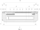
FIG. 5 is a second schematic diagram of the display module provided by the embodiment of the application. - The following description of the embodiments is made with reference to additional illustrations to illustrate specific embodiments that the present invention can be implemented. The direction terms mentioned in the invention, such as [up], [down], [front], [back], [left], [right], [inside], [outside], [side], etc., are only the direction of reference to the additional schematic. Therefore, the directional terms used are intended to illustrate and understand the invention, not to limit the invention. In the figure, units with similar structures are represented by the same label.
- In the description of the present application, it should be understood that the terms "first" and "second" are only used for descriptive purposes and cannot be understood as indicating or implying relative importance or implicitly indicating the number of indicated technical features. Thus, the features defining "first" and "second" may explicitly or implicitly include one or more of the features. In the description of this application, "multiple" means two or more, unless otherwise expressly and specifically defined.
- In the description of the application, it should be noted that, unless otherwise clearly specified and limited, the terms "installation", "connection" and "connection" should be understood in a broad sense, for example, it can be fixed connection, removable connection, or integrated connection; it can be mechanical connection, electrical connection or mutual communication; it can be directly connected or indirectly connected through an intermediate medium, it can be the connection within two elements or the interaction relationship between two elements. For those skilled in the art, the specific meaning of the above terms in the application can be understood according to the specific circumstances.
- The technical scheme of the application is described in combination with specific embodiments.
- Please refer to
FIG.2 to FIG. 4 , The embodiment of the present application provides a display module including a metal backframe 10 and adisplay panel 20 disposed on the metal backframe 10, wherein the display panel includes: - a
first substrate 21, wherein at least one end of thefirst substrate 21 is disposed on the metal backframe 10; and - a
second substrate 22 disposed opposite to thefirst substrate 21 and is located between thefirst substrate 21 and the metal backframe 10, wherein aliquid crystal layer 23 is disposed between thefirst substrate 21 and thesecond substrate 22; and - wherein, the
first substrate 21 includes a base and a thin film transistor layer disposed on one side of the base close to the second substrate. - It can be understood that, at present, as shown in
FIG. 1 , vehicle display modules mainly include aframe body 1, apanel body 2 and a fixed cover 3, fixed cover 3 is connected to theframe body 1 through the fixingtape 9 to form aclosed space 400, the panelmain body 2 is integrally disposed in theclosed space 400 and is connected to the fixed cover 3 byadhesive 8. The panelmain body 2 includes a laminated firstpolarizing structure 4, anarray substrate 5, acolor filter substrate 6 and a laminated secondpolarizing structure 7. Thepanel body 2 is bonded to the fixed cover 3 on the side where the secondpolarizing structure 7 is provided. This structure using adhesive 8 to connect the fixed cover plate 3 and thepanel body 2 is easy to lead to excessive thickness of the vehicle display module, which is not suitable for the development demand of thinning the vehicle display module; In this embodiment, by disposing thefirst substrate 21 of thedisplay panel 20 on the metal backframe 10, and disposing thesecond substrate 22 of thedisplay panel 20 opposite thefirst substrate 21 and located between thefirst substrate 21 and the metal backframe 10, the complexity of the overall structure of the display module is reduced. Obviously, this structure of that thefirst substrate 21 of the display panel directly disposes on the metal backframe 10 omits the adhesive 8, the fixed cover plate 3 and other related original films, and the thickness of the display module is reduced, to meet the thinning requirements of the display module. - It is worth noting that, as shown in
FIG. 1 , at present, the vehicle display module is assembled through the connection between the fixed cover plate 3 and theframe 1 and he connection between the fixed cover plate 3 and thepanel body 2 respectively. Specifically, the structure in which the fixed cover plate 3 and thepanel body 2 are bonded and fixed by adhesive 8 is also easy to increase the difficulty of the vehicle display module process. In this embodiment, By directly setting thefirst substrate 21 of thedisplay panel 20 on the metal backframe 10, the original functional films such as fixed cover plate 3 and adhesive 8 are eliminated, that is, the manufacturing difficulty of the display module is reduced and the yield of the display module is improved; in addition, in this embodiment, thefirst substrate 21 includes asubstrate 211 and a thinfilm transistor layer 212 disposed on the side of thesubstrate 211 close to thesecond substrate 22. Thesubstrate 211 is a hard substrate to protect other functional films in the display module., specifically, thesubstrate 211 can be a glass substrate. - It should be noted that, the
display panel 20 further includes afirst polarizer 24 and asecond polarizer 25. Thefirst polarizer 24 is disposed on the side of thefirst substrate 21 away from thesecond substrate 22, and thesecond polarizer 25 is disposed on the side of thesecond substrate 22 away from the first substrate 21.The display module further includes abacklight module 26 disposed between thedisplay panel 20 and the metal backframe 10 and located in a holdingspace 100, thebacklight module 26 at least includes astacked reflector 261, alight guide plate 262 and anoptical film 263. Specifically, thebacklight module 26 is a side entry structure or a straight down structure, which is not limited here. - In one embodiment, please refer to
FIG. 2 , wherein the display panel further includes an opposingarea 200 and a connectingarea 300 surrounding the opposingarea 200; - the
first substrate 21 further includes adisplay driving part 213 located in the opposingarea 200 and a first connectingpart 214 located in the connectingarea 300; and - the metal back
frame 10 includes ametal back cover 11 disposed opposite to thefirst substrate 21 and ametal support plate 12 extending along a direction from the peripheral side of the metal back cover to thefirst substrate 21, and themetal support plate 12 is located in the connectingarea 300 and connected to the first connectingpart 214. - It can be understood that the
display panel 20 includes an opposingarea 200 and a connectingarea 300 surrounding the opposingarea 200, and divides thefirst substrate 21 into adisplay driving unit 213 located in the opposingarea 200 and afirst connection part 214 located in the connectingarea 300, and the metal backframe 10 is divided into ametal back cover 11 disposed opposite to thefirst substrate 21 and ametal support plate 12 extending from the peripheral side of themetal back cover 11 to the direction of thefirst substrate 21. Themetal support plate 12 is located in the connectingarea 300 and connected to thefirst connection part 214, to realize the connection between thefirst substrate 21 and the metal backframe 10 in the connectingarea 300. - It should be noted that the first connecting
part 214 can be disposed around thedisplay driving part 213 and connected to themetal support plate 12, thesecond substrate 22 can be disposed opposite to thedisplay driving part 213 and located in the opposingarea 200, and thefirst substrate 21, themetal back cover 11 and themetal support plate 12 can be enclosed to form a holdingspace 100. In this embodiment, thesecond substrate 22 can be located in the holding space, thesecond substrate 22 can be disposed opposite to thedisplay driving unit 213 and located in the opposingarea 200, that is, thesecond substrate 22 is aligned with thedisplay driving unit 213, and theliquid crystal layer 23 is disposed between thesecond substrate 22 and thedisplay driving part 213, to realize the function of driving the liquid crystal deflection in theliquid crystal layer 23. - In one embodiment, please refer to
FIG. 2 to FIG. 4 , the display module further includes a first conductive adhesive 30 located in the connectingarea 300 and connecting thefirst substrate 21 with the metal backframe 10; and
the thinfilm transistor layer 212 includes a firstelectrostatic discharge terminal 2120 located in the connectingarea 300, and the firstconductive adhesive 30 is electrically connecing themetal support plate 12 with the firstelectrostatic discharge terminal 2120. - It can be understood that, as shown in
FIG. 1 , at present, the vehicle display module is assembled through the connection of the fixed cover plate 3 with theframe 1 and thepanel body 2 respectively, wherein the fixed cover plate 3 is connected to thepanel body 2 through the adhesive 8, and the fixed cover plate 3 is connected to theframe 1 through the fixedadhesive 9, so that the static electricity generated on thepanel body 2 cannot be released to theframe 1, the electrostatic discharge capacity of the vehicle display module is low, which affects the use experience. In this embodiment, the display module includes a first conductive adhesive 30 located in the connectingarea 300 and connecting thefirst substrate 21 with the metal backframe 10, and the thinfilm transistor layer 212 includes a firstelectrostatic discharge terminal 2120 located in the connectingarea 300, which electrically connected themetal support plate 12 to the firstelectrostatic discharge terminal 2120 through the firstconductive adhesive 30. Thus, it is convenient to release the static electricity on the thinfilm transistor layer 212 to the metal backframe 10, and the static electricity release ability of the display module is improved; specifically, the firstconductive adhesive 30 may be a conductive foam tape or an optical adhesive embedded with conductive gold balls. - In one embodiment, please refer to
FIG. 2 to FIG. 4 , thinfilm transistor layer 212 is provided with afirst groove 2121 located in the connectingarea 300, and the firstelectrostatic discharge terminal 2120 is disposed in thefirst groove 2121; and
one end of the firstconductive adhesive 30 is electrically connected to themetal support plate 12, and another end of the firstconductive adhesive 30 is disposed in thefirst groove 2121 and is electrically connected to the firstelectrostatic discharge terminal 2120. - It can be understood that the thin
film transistor layer 212 includes afirst groove 2121 located in the connectingarea 300, and the firstelectrostatic discharge terminal 2120 is disposed in thefirst groove 2121, and one end of the firstconductive adhesive 30 is electrically connected to themetal support plate 12, another end of the firstconductive adhesive 30 is disposed in thefirst groove 2121 and electrically connected to the firstelectrostatic discharge terminal 2120. By setting thefirst groove 2121, one end of the firstconductive adhesive 30 is disposed in thefirst groove 2121 and electrically connected to the firstelectrostatic discharge terminal 2120, the firstconductive adhesive 30 is prevented from being squeezed between the first panel and the metal backframe 10, which further reduces the thickness of the display module, and also ensures the full contact between the firstconductive adhesive 30 and the firstelectrostatic discharge terminal 2120. - In one embodiment, please refer to
FIG.3 to FIG. 4 , wherein tthe thinfilm transistor layer 212 further includes afirst metal layer 2122 disposed on thesubstrate 211, asecond metal layer 2123 disposed on thefirst metal layer 2122, and an insulating layer stacked with thefirst metal layer 2122 and thesecond metal layer 2123, and thefirst groove 2121 is defined in the insulating layer and located in the connectingarea 300; and
thefirst metal layer 2122 includes the firstelectrostatic discharge terminal 2120, or thesecond metal layer 2123 includes the firstelectrostatic discharge terminal 2120. - It can be understood that the thin
film transistor layer 212 includes afirst metal layer 2122 disposed on thesubstrate 211, asecond metal layer 2123 disposed on thefirst metal layer 2122, and an insulating layer stacked with thefirst metal layer 2122 and thesecond metal layer 2123, thefirst groove 2121 is disposed on the insulating layer and located in the connectingarea 300. Thefirst metal layer 2122 includes the firstelectrostatic discharge terminal 2120, or thesecond metal layer 2123 includes the firstelectrostatic discharge terminal 2120, that is, thefirst metal layer 2122 and the firstelectrostatic discharge terminal 2120 are disposed on the same layer, or thesecond metal layer 2123 and the firstelectrostatic discharge terminal 2120 are disposed on the same layer. Thus, the static electricity on the thinfilm transistor layer 212 can be released to the metal backframe 10 without adding a new film layer structure. In this embodiment, thefirst metal layer 2122 can further include a gate located in the opposingarea 200, and thesecond metal layer 2123 can further include a source and a drain located in the opposingarea 200. - In one embodiment, please refer to
FIG.3 , thesecond metal layer 2123 includes the firstelectrostatic discharge terminal 2120, and the insulating layer includes a first insulatingsublayer 2124 disposed on a side of thesecond metal layer 2123 away from thesubstrate 211; and
thefirst groove 2121 corresponds to the firstelectrostatic discharge terminal 2120 and is defined in the first insulatingsublayer 2124. - It can be understood that the
second metal layer 2123 includes the firstelectrostatic discharge terminal 2120, that is, thesecond metal layer 2123 and the firstelectrostatic discharge terminal 2120 are disposed on the same layer, and the insulating layer includes thefirst insulator layer 2124 disposed on the side of thesecond metal layer 2123 away from thesubstrate 211. Thefirst groove 2121 corresponds to the firstelectrostatic discharge terminal 2120 and is defined in thefirst insulator layer 2124, so that the firstconductive adhesive 30 can be electrically connected to the firstelectrostatic discharge terminal 2120 through thefirst groove 2121. - In one embodiment, please refer to
FIG.4 , thefirst metal layer 2122 includes the firstelectrostatic discharge terminal 2120, and the insulating layer includes a first insulatingsublayer 2124 disposed on one side of thesecond metal layer 2123 away from thesubstrate 211, and a second insulatingsublayer 2125 disposed between thefirst metal layer 2122 and thesecond metal layer 2123; and
thefirst groove 2121 corresponds to the firstelectrostatic discharge terminal 2120 and is defined in the first insulatingsublayer 2124 and the second insulatingsublayer 2125. - It can be understood that the
first metal layer 2122 includes the firstelectrostatic discharge terminal 2120, that is, thefirst metal layer 2122 and the firstelectrostatic discharge terminal 2120 are disposed on the same layer, and the insulating layer includes thefirst insulator layer 2124 disposed on the side of thesecond metal layer 2123 away from thesubstrate 211. Asecond insulator layer 2125 disposed between thefirst metal layer 2122 and thesecond metal layer 2123, thefirst groove 2121 corresponds to the firstelectrostatic discharge terminal 2120 and is defined in thefirst insulator layer 2124 and thesecond insulator layer 2125 so that thefirst groove 2121 passes through thefirst insulator layer 2124 and thesecond insulator layer 2125. The depth of thefirst groove 2121 is maximized, so that the volume containing the firstconductive adhesive 30 is increased, compared with the structure disposed on the same layer of thesecond metal layer 2123 and the firstelectrostatic discharge terminal 2120, the thickness of the display module is further reduced. - In one embodiment, please refer to
FIG.2 to FIG.4 , themetal support plate 12 is provided with asecond groove 121 located in the connectingarea 300; and
one end of the firstconductive adhesive 30 is disposed in thesecond groove 121 and is electrically connected to themetal support plate 12, and another end of the firstconductive adhesive 30 is disposed in thefirst groove 2121 and is electrically connected to the firstelectrostatic discharge terminal 2120. - It can be understood that the
metal support plate 12 is provided with asecond groove 121 located in the connectingarea 300, and the thinfilm transistor layer 212 is provided with afirst groove 2121 located in the connectingarea 300, so that one end of the firstconductive adhesive 30 is disposed in thesecond groove 121 and electrically connected to themetal support plate 12, another end of the firstconductive adhesive 30 is disposed in thefirst groove 2121 and electrically connected to the firstelectrostatic discharge terminal 2120, so that both ends of the firstconductive adhesive 30 are disposed in thefirst groove 2121 and thesecond groove 121 as much as possible, reducing the thickness of the display module, the electrostatic discharge on the thinfilm transistor layer 212 to the metal backframe 10 is also realized. - In one embodiment, the
second groove 121 is annularly defined in themetal support plate 12 and disposed around the opposingarea 200. It can be understood that thesecond groove 121 is a ring and annularly disposed around the opposingarea 200, and the firstconductive adhesive 30 is at least disposed in thesecond groove 121, so as to facilitate the bonding of thefirst substrate 21 and the metal backframe 10 through the firstconductive adhesive 30, and increase the area of electrical connection between the metal backframe 10 and the firstconductive adhesive 30 at the same time, it is convenient to discharge static electricity on the thinfilm transistor layer 212 to the metal backframe 10. - In one embodiment, please refer to
FIG. 2 to FIG. 4 , an orthograph projection of the firstconductive adhesive 30 on thesubstrate 211 overlaps an orthograph projection of the firstelectrostatic discharge terminal 2120 on thesubstrate 211. - It can be understood that the orthograph projection of the first
conductive adhesive 30 on thesubstrate 211 overlaps the orthograph projection of the firstelectrostatic discharge terminal 2120 on thesubstrate 211, that is, the firstconductive adhesive 30 is completely covered on the firstelectrostatic discharge terminal 2120, so that the firstconductive adhesive 30 is fully electrically connected to the firstelectrostatic discharge terminal 2120, it is convenient to discharge static electricity on the thinfilm transistor layer 212 to the metal backframe 10. In one embodiment, please refer toFIG. 5 , the connectingarea 300 includes a first connectingsubarea 310 and a second connectingsubarea 320, themetal support plate 12 includes afirst support plate 121 located in the first connectingsubarea 310 and asecond support plate 122 located in the second connectingsubarea 320, and a distance from thesecond support plate 122 to thefirst substrate 21 is greater than a distance from thefirst support plate 121 to thefirst substrate 21; and
thesecond substrate 22 includes a second connectingpart 221 located in the second connectingsubarea 320, thefirst support plate 121 and the first connectingpart 214 are connected in the first connectingsubarea 310, and thesecond support plate 122 and the second connectingpart 221 are connected in the second connectingsubarea 320. - It can be understood that the connecting
area 300 includes a first connectingsubarea 310 and a second connectingsubarea 320, and themetal support plate 12 includes afirst support plate 121 located in the first connectingsubarea 310 and asecond support plate 122 located in the second connectingsubarea 320, and the spacing between thesecond support plate 122 and thefirst substrate 21 is set to be greater than the spacing between thefirst support plate 121 and thefirst substrate 21, so that thefirst substrate 21 extends into the second connectingsubarea 320, so that themetal support plate 12 can be connected to thefirst substrate 21 in the first connectingsubarea 310. And themetal support plate 12 is connected to thesecond substrate 22 in the second connectingsubarea 320, specifically, thesecond substrate 22 includes a second connectingpart 221 located in the second connectingsubarea 320, and thefirst support plate 121 and the first connectingpart 214 are connected in the first connectingsubarea 310, thesecond support plate 122 and the second connectingpart 221 are connected in the second connectingsubarea 320, thereby reducing the thickness of the display module to meet the thinning requirements of the display module. - In one embodiment, please refer to
FIG.5 , the display module further includes a first conductive adhesive 30 located in the first connectingsubarea 310 and connecting the first connectingpart 214 with hefirst support plate 121, and a second conductive adhesive 40 located in the second connectingsubarea 320 and connecting the second connectingpart 221 with thesecond support plate 122; and
thefirst substrate 21 further includes a firstelectrostatic discharge terminal 2120 located in the first connectingsubarea 310, thesecond substrate 22 further includes a secondelectrostatic discharge terminal 2200 located in the second connectingsubarea 320, the firstconductive adhesive 30 is electrically connected thefirst support plate 121 with the firstelectrostatic discharge terminal 2120, and the secondconductive adhesive 40 is electrically connected thesecond support plate 122 with the secondelectrostatic discharge terminal 2200. - It can be understood that, as shown in
FIG. 1 , at present, the vehicle display module is assembled with theframe 1 and thepanel body 2 respectively through the connection of the fixed cover plate 3, wherein the fixed cover plate 3 is connected with thepanel body 2 through the adhesive 8. And the fixed cover plate 3 is connected with theframe 1 through the fixedadhesive 9, so that the static electricity generated on thepanel body 2 cannot be released to theframe 1. The electrostatic discharge capacity of the vehicle display module is low, which affects the use experience. In this embodiment, the display module includes a first conductive adhesive 30 located in the first connectingsubarea 310 and connecting the first connectingpart 214 with thefirst support plate 121, and a second conductive adhesive 40 located in the second connectingsubarea 320 and connecting the second connectingpart 221 with thesecond support plate 122, and thefirst substrate 21 further includes a firstelectrostatic discharge terminal 2120 located in the first connectingsubarea 310. Thesecond substrate 22 includes a secondelectrostatic discharge terminal 2200 located in the second connectingsubarea 320, and the firstconductive adhesive 30 is electrically connected thefirst support plate 121 with the firstelectrostatic discharge terminal 2120, the second conductive adhesive 40 electrically connected thesecond support plate 122 with the secondelectrostatic discharge terminal 2200, and electrically connected thefirst support plate 121 with the firstelectrostatic discharge terminal 2120 through the firstconductive adhesive 30, so as to facilitate the electrostatic discharge on thefirst substrate 21 to the metal backframe 10, thesecond support plate 122 and the secondelectrostatic discharge terminal 2200 are electrically connected through the secondconductive adhesive 40, so as to facilitate the electrostatic discharge on thesecond substrate 22 to the metal back frame, and improve the electrostatic discharge capacity of the display module. Specifically, the firstconductive adhesive 30 and the secondconductive adhesive 40 may be conductive foam tape or optical adhesive embedded with conductive golden balls. - It should be noted that the orthograph projection of the second
conductive adhesive 40 on thefirst substrate 21 can overlaps the orthograph projection of the secondelectrostatic discharge terminal 2200 on thefirst substrate 21, and the secondelectrostatic discharge terminal 2200 can be electrically connected to the metal layer in the second substrate 22., the specific connection structure is not limited here. - The embodiment of the application further provides a display device, which includes the display module and the device body as in the previous embodiment, and the display module and the device main body are combined into one body.
- The present application reduces the complexity of the overall structure of the display module by setting the
first substrate 21 of thedisplay panel 20 on the metal backframe 10, and setting thesecond substrate 22 of thedisplay panel 20 opposite to thefirst substrate 21 and located between thefirst substrate 21 and the metal backframe 10. Obviously, this structure of directly setting thefirst substrate 21 of thedisplay panel 20 on the metal backframe 10, the original film layers such asadhesive 8 and fixed cover plate 3 are omitted, and the thickness of the display module is reduced to meet the thinning requirements of the display module. - To sum up, although the invention has been disclosed as above in the preferred embodiment, the above preferred embodiment is not intended to limit the invention, ordinary technicians in the art can make various changes and refinements without departing from the scope of the invention, therefore, the protection scope of the invention shall be subject to the scope defined in the claims.
Claims (20)
- A display module comprising a metal back frame and a display panel disposed on the metal back frame, wherein the display panel comprises:a first substrate, wherein at least one end of the first substrate is disposed on the metal back frame; anda second substrate disposed opposite to the first substrate and located between the first substrate and the metal back frame, wherein a liquid crystal layer is disposed between the first substrate and the second substrate; andwherein the first substrate comprises a base and a thin film transistor layer disposed on one side of the base close to the second substrate.
- The display module according to claim 1, wherein the display panel further comprises an opposing area and a connecting area surrounding the opposing area;the first substrate further comprises a display driving part located in the opposing area and a first connecting part located in the connecting area; andthe metal back frame comprises a metal back cover disposed opposite to the first substrate and a metal support plate extending along a direction from the peripheral side of the metal back cover to the first substrate, and the metal support plate is located in the connecting area and connected to the first connecting part.
- The display module according to claim 2, wherein the display module further comprises a first conductive adhesive located in the connecting area and connecting the first substrate with the metal back frame; and
the thin film transistor layer comprises a first electrostatic discharge terminal located in the connecting area, and the first conductive adhesive is electrically connected to the metal support platewith the first electrostatic discharge terminal. - The display module according to claim 3, wherein the thin film transistor layer is provided with a first groove located in the connecting area, and the first electrostatic discharge terminal is disposed in the first groove; and
one end of the first conductive adhesive is electrically connected to the metal support plate, and another end of the first conductive adhesive is disposed in the first groove and is electrically connected to the first electrostatic discharge terminal. - The display module according to claim 4, wherein the thin film transistor layer further comprises a first metal layer disposed on a substrate, a second metal layer disposed on the first metal layer, and an insulating layer stacked with the first metal layer and the second metal layer, and the first groove is defined in the insulating layer and located in the connecting area; and
the first metal layer comprises the first electrostatic discharge terminal, or the second metal layer comprises the first electrostatic discharge terminal. - The display module according to claim 5, wherein the second metal layer comprises the first electrostatic discharge terminal, and the insulating layer comprises a first insulating sublayer disposed on a side of the second metal layer away from the substrate; and
the first groove corresponds to the first electrostatic discharge terminal and is defined in the first insulating sublayer. - The display module according to claim 5, wherein the first metal layer comprises the first electrostatic discharge terminal, and the insulating layer comprises a first insulating sublayer disposed on one side of the second metal layer away from the substrate, and a second insulating sublayer disposed between the first metal layer and the second metal layer; and
the first groove corresponds to the first electrostatic discharge terminal and is defined in the first insulating sublayer and the second insulating sublayer. - The display module according to claim 4, wherein the metal support plate is provided with a second groove located in the connecting area; and
one end of the first conductive adhesive is disposed in the second groove and is electrically connected to the metal support plate, and another end of the first conductive adhesive is disposed in the first groove and is electrically connected to the first electrostatic discharge terminal. - The display module according to claim 8, wherein the second groove is annularly defined in the metal support plate and disposed around the opposing area.
- The display module according to claim 3, wherein an orthograph projection of the first conductive adhesive on the substrate overlaps an orthograph projection of the first electrostatic discharge terminal on the substrate.
- The display module according to claim 2, wherein the first connecting part is disposed around the display driving part and connected to the metal support plate, and the second substrate is disposed opposite to the display driving part and is located in the opposing area.
- The display module according to claim 2, wherein the connecting area comprises a first connecting subarea and a second connecting subarea, the metal support plate comprises a first support plate located in the first connecting subarea and a second support plate located in the second connecting subarea, and a distance from the second support plate to the first substrate is greater than a distance from the first support plate to the first substrate; and
the second substrate comprises a second connecting part located in the second connecting subarea, the first support plate and the first connecting part are connected in the first connecting subarea, and the second support plate and the second connecting part are connected in the second connecting subarea. - The display module according to claim 12, wherein the display module further comprises a first conductive adhesive located in the first connecting subarea and connecting the first connecting part with the first support plate, and a second conductive adhesive located in the second connecting subarea and connecting the second connecting part with the second support plate; and
the first substrate further comprises a first electrostatic discharge terminal located in the first connecting subarea, the second substrate further comprises a second electrostatic discharge terminal located in the second connecting subarea, the first conductive adhesive is electrically connected the first support plate with the first electrostatic discharge terminal, and the second conductive adhesive is electrically connected the second support plate with the second electrostatic discharge terminal. - A display device comprising a display module and a device main body, wherein the display module and the device main body are combined into one body;
wherein the display module comprises a metal back frame and a display panel disposed on the metal back frame, and the display panel comprises:a first substrate, at least one end of the first substrate is disposed on the metal back frame; anda second substrate disposed opposite to the first substrate and is located between the first substrate and the metal back frame, a liquid crystal layer is disposed between the first substrate and the second substrate; andwherein the first substrate comprises a base and a thin film transistor layer disposed on one side of the base close to the second substrate. - The display device according to claim 14, wherein the display panel further comprises an opposing area 200 and a connecting area surrounding the opposing area 200;the first substrate further comprises a display driving part located in the opposing area 200 and a first connecting part located in the connecting area; andthe metal back frame comprises a metal back cover disposed opposite to the first substrate and a metal support plate extending along a direction from the peripheral side of the metal back cover to the first substrate, and the metal support plate is located in the connecting area and connected to the first connecting part.
- The display device according to claim 15, wherein the display module further comprises a first conductive adhesive located in the connecting area and connectingthe first substrate with the metal back frame; and
the thin film transistor layer comprises a first electrostatic discharge terminal located in the connecting area, and the first conductive adhesive is electrically connected the metal support plate with the first electrostatic discharge terminal. - The display device according to claim 16, wherein the thin film transistor layer is provided with a first groove located in the connecting area, and the first electrostatic discharge terminal is disposed in the first groove; and
one end of the first conductive adhesive is electrically connected to the metal support plate, and another end of the first conductive adhesive is disposed in the first groove and is electrically connected to the first electrostatic discharge terminal. - The display device according to claim 17, wherein the thin film transistor layer further comprises a first metal layer disposed on the substrate, a second metal layer disposed on the first metal layer, and an insulating layer stacked with the first metal layer and the second metal layer, and the first groove is defined in the insulating layer and located in the connecting area; and
the first metal layer comprises the first electrostatic discharge terminal, or the second metal layer comprises the first electrostatic discharge terminal. - The display device according to claim 15, wherein the connecting area comprises a first connecting subarea and a second connecting subarea, the metal support plate comprises a first support plate located in the first connecting subarea and a second support plate located in the second connecting subarea, and a distance from the second support plate to the first substrate is greater than a distance from the first support plate to the first substrate; and
the second substrate comprises a second connecting part located in the second connecting subarea, the first support plate and the first connecting part are connected in the first connecting subarea, and the second support plate and the second connecting part are connected in the second connecting subarea. - The display device according to claim 19, wherein the display module further comprises a first conductive adhesive located in the first connecting subarea and connecting the first connecting part with the first support plate, and a second conductive adhesive located in the second connecting subarea and connecting the second connecting part with the second support plate; and
the first substrate further comprises a first electrostatic discharge terminal located in the first connecting subarea, the second substrate further comprises a second electrostatic discharge terminal located in the second connecting subarea, the first conductive adhesive is electrically connected the first support plate with the first electrostatic discharge terminal, and the second conductive adhesive is electrically connected the second support plate with the second electrostatic discharge terminal.
Applications Claiming Priority (2)
| Application Number | Priority Date | Filing Date | Title |
|---|---|---|---|
| CN202111581099.5A CN114296267B (en) | 2021-12-22 | 2021-12-22 | A display module and a display device |
| PCT/CN2021/141235 WO2023115546A1 (en) | 2021-12-22 | 2021-12-24 | Display module and display device |
Publications (2)
| Publication Number | Publication Date |
|---|---|
| EP4455774A1 true EP4455774A1 (en) | 2024-10-30 |
| EP4455774A4 EP4455774A4 (en) | 2025-10-22 |
Family
ID=80969682
Family Applications (1)
| Application Number | Title | Priority Date | Filing Date |
|---|---|---|---|
| EP21827537.8A Pending EP4455774A4 (en) | 2021-12-22 | 2021-12-24 | DISPLAY MODULE AND DISPLAY DEVICE |
Country Status (5)
| Country | Link |
|---|---|
| US (1) | US12158681B2 (en) |
| EP (1) | EP4455774A4 (en) |
| JP (1) | JP7490682B2 (en) |
| CN (1) | CN114296267B (en) |
| WO (1) | WO2023115546A1 (en) |
Families Citing this family (1)
| Publication number | Priority date | Publication date | Assignee | Title |
|---|---|---|---|---|
| KR20230126241A (en) * | 2022-02-21 | 2023-08-30 | 삼성디스플레이 주식회사 | display device |
Family Cites Families (27)
| Publication number | Priority date | Publication date | Assignee | Title |
|---|---|---|---|---|
| JP4010124B2 (en) | 1995-01-11 | 2007-11-21 | セイコーエプソン株式会社 | Power supply circuit, liquid crystal display device and electronic device |
| JP2000137446A (en) | 1998-11-02 | 2000-05-16 | Hitachi Ltd | Liquid crystal display |
| JP2004354606A (en) | 2003-05-28 | 2004-12-16 | Sony Corp | Liquid crystal display device and method of manufacturing the same |
| JP2006184349A (en) * | 2004-12-27 | 2006-07-13 | Casio Comput Co Ltd | Display module and manufacturing method thereof |
| JP4353266B2 (en) * | 2007-04-05 | 2009-10-28 | エプソンイメージングデバイス株式会社 | Electro-optical device and electronic apparatus |
| JP5079715B2 (en) * | 2009-01-16 | 2012-11-21 | 株式会社ジャパンディスプレイウェスト | Liquid crystal display |
| KR101681884B1 (en) | 2009-03-27 | 2016-12-05 | 가부시키가이샤 한도오따이 에네루기 켄큐쇼 | Semiconductor device, display device, and electronic appliance |
| CN101866069A (en) * | 2009-04-17 | 2010-10-20 | 群康科技(深圳)有限公司 | Display device |
| JP5544749B2 (en) | 2009-04-27 | 2014-07-09 | セイコーエプソン株式会社 | Electro-optical device and electronic apparatus |
| US8456586B2 (en) * | 2009-06-11 | 2013-06-04 | Apple Inc. | Portable computer display structures |
| TWI442361B (en) | 2011-03-22 | 2014-06-21 | Innolux Corp | Display module and manufacturing method thereof |
| CN202067045U (en) | 2011-05-10 | 2011-12-07 | 深圳市华星光电技术有限公司 | Liquid crystal display device and rear shell of liquid crystal display device |
| TWI467270B (en) * | 2011-07-01 | 2015-01-01 | Au Optronics Corp | Carrier and display device using same |
| US9274359B2 (en) | 2012-06-20 | 2016-03-01 | Apple Inc. | Electronic device display chassis |
| JP6627447B2 (en) * | 2015-11-19 | 2020-01-08 | 三菱電機株式会社 | Liquid crystal display |
| CN205193388U (en) | 2015-11-25 | 2016-04-27 | 武汉天马微电子有限公司 | Display device |
| KR102599883B1 (en) | 2016-11-15 | 2023-11-09 | 삼성전자주식회사 | Display apparatus |
| CN106526943B (en) * | 2017-01-12 | 2019-06-14 | 京东方科技集团股份有限公司 | A liquid crystal display device |
| CN109037468A (en) | 2017-06-09 | 2018-12-18 | 上海和辉光电有限公司 | A kind of display panel |
| CN206833100U (en) * | 2017-06-27 | 2018-01-02 | 京东方科技集团股份有限公司 | Display panel and display device |
| KR20190034368A (en) * | 2017-09-22 | 2019-04-02 | 삼성디스플레이 주식회사 | Backlight unit and display device including the same |
| CN108254961A (en) | 2018-02-12 | 2018-07-06 | 京东方科技集团股份有限公司 | A kind of display panel, display module and display device |
| US20200363673A1 (en) * | 2019-05-17 | 2020-11-19 | Sharp Kabushiki Kaisha | Display panel and display apparatus |
| CN110703500A (en) * | 2019-10-25 | 2020-01-17 | 京东方科技集团股份有限公司 | Display panels and display devices |
| CN110928061B (en) | 2019-11-29 | 2022-04-26 | 武汉华星光电技术有限公司 | Display panel and display device |
| CN111679504B (en) | 2020-06-28 | 2022-06-10 | 武汉华星光电技术有限公司 | Backlight module and display panel |
| CN214122615U (en) * | 2020-10-23 | 2021-09-03 | 京东方科技集团股份有限公司 | Display module and display device |
-
2021
- 2021-12-22 CN CN202111581099.5A patent/CN114296267B/en active Active
- 2021-12-24 US US17/623,609 patent/US12158681B2/en active Active
- 2021-12-24 WO PCT/CN2021/141235 patent/WO2023115546A1/en not_active Ceased
- 2021-12-24 EP EP21827537.8A patent/EP4455774A4/en active Pending
- 2021-12-24 JP JP2021577677A patent/JP7490682B2/en active Active
Also Published As
| Publication number | Publication date |
|---|---|
| JP2024502910A (en) | 2024-01-24 |
| US12158681B2 (en) | 2024-12-03 |
| WO2023115546A1 (en) | 2023-06-29 |
| EP4455774A4 (en) | 2025-10-22 |
| CN114296267A (en) | 2022-04-08 |
| JP7490682B2 (en) | 2024-05-27 |
| US20240036425A1 (en) | 2024-02-01 |
| CN114296267B (en) | 2023-09-05 |
Similar Documents
| Publication | Publication Date | Title |
|---|---|---|
| CN100480811C (en) | Display device | |
| US6903794B2 (en) | Semiconductor device, liquid crystal module adopting same, method of manufacturing liquid crystal module, and electronic equipment adopting same | |
| US9201459B2 (en) | Portable terminal | |
| US20070252922A1 (en) | Liquid crystal display device | |
| US20110123266A1 (en) | Device with ring-shaped fixing member | |
| WO2006126376A1 (en) | Liquid crystal display | |
| JP2000353416A (en) | Flat panel display | |
| US20100265430A1 (en) | Display device with conductive masking film for discharging static electricity | |
| US12158681B2 (en) | Display module and display device | |
| JPH10268268A (en) | Liquid crystal display panel, liquid crystal display device and electronic equipment using the same | |
| JP3275764B2 (en) | Liquid crystal display panel, liquid crystal display device and electronic equipment using the same | |
| CN112838112A (en) | Display panel and display device | |
| US20240411160A1 (en) | Liquid crystal display panel and liquid crystal display device | |
| JP2006330230A (en) | Liquid crystal display | |
| CN115145071A (en) | Display module and display device | |
| JP3719362B2 (en) | Display device and electronic device | |
| WO2019214094A1 (en) | Oled display structure and oled display screen | |
| WO2019237269A1 (en) | Display screen assembly, electronic device and fabrication method therefor | |
| CN113589584B (en) | Backlight modules, LCD modules and LCD monitors | |
| CN115755457A (en) | Display module and display device | |
| CN223742904U (en) | Display device | |
| JP3744289B2 (en) | Display device and electronic apparatus equipped with the same | |
| CN112835227A (en) | Backlight modules and electronic equipment | |
| JP3719361B2 (en) | Display device and electronic device including the same | |
| CN115016184B (en) | Display module assembly and on-vehicle display device |
Legal Events
| Date | Code | Title | Description |
|---|---|---|---|
| STAA | Information on the status of an ep patent application or granted ep patent |
Free format text: STATUS: UNKNOWN |
|
| STAA | Information on the status of an ep patent application or granted ep patent |
Free format text: STATUS: THE INTERNATIONAL PUBLICATION HAS BEEN MADE |
|
| PUAI | Public reference made under article 153(3) epc to a published international application that has entered the european phase |
Free format text: ORIGINAL CODE: 0009012 |
|
| STAA | Information on the status of an ep patent application or granted ep patent |
Free format text: STATUS: REQUEST FOR EXAMINATION WAS MADE |
|
| 17P | Request for examination filed |
Effective date: 20211231 |
|
| AK | Designated contracting states |
Kind code of ref document: A1 Designated state(s): AL AT BE BG CH CY CZ DE DK EE ES FI FR GB GR HR HU IE IS IT LI LT LU LV MC MK MT NL NO PL PT RO RS SE SI SK SM TR |
|
| DAV | Request for validation of the european patent (deleted) | ||
| DAX | Request for extension of the european patent (deleted) | ||
| A4 | Supplementary search report drawn up and despatched |
Effective date: 20250923 |
|
| RIC1 | Information provided on ipc code assigned before grant |
Ipc: G02F 1/1333 20060101AFI20250917BHEP Ipc: G02F 1/1362 20060101ALI20250917BHEP |