EP4451828A1 - Anzeigesubstrat und herstellungsverfahren dafür sowie anzeigevorrichtung - Google Patents
Anzeigesubstrat und herstellungsverfahren dafür sowie anzeigevorrichtung Download PDFInfo
- Publication number
- EP4451828A1 EP4451828A1 EP23838642.9A EP23838642A EP4451828A1 EP 4451828 A1 EP4451828 A1 EP 4451828A1 EP 23838642 A EP23838642 A EP 23838642A EP 4451828 A1 EP4451828 A1 EP 4451828A1
- Authority
- EP
- European Patent Office
- Prior art keywords
- light
- pixel
- sub
- base substrate
- shielding layer
- Prior art date
- Legal status (The legal status is an assumption and is not a legal conclusion. Google has not performed a legal analysis and makes no representation as to the accuracy of the status listed.)
- Pending
Links
Images


Classifications
-
- H—ELECTRICITY
- H10—SEMICONDUCTOR DEVICES; ELECTRIC SOLID-STATE DEVICES NOT OTHERWISE PROVIDED FOR
- H10K—ORGANIC ELECTRIC SOLID-STATE DEVICES
- H10K59/00—Integrated devices, or assemblies of multiple devices, comprising at least one organic light-emitting element covered by group H10K50/00
- H10K59/50—OLEDs integrated with light modulating elements, e.g. with electrochromic elements, photochromic elements or liquid crystal elements
-
- H—ELECTRICITY
- H10—SEMICONDUCTOR DEVICES; ELECTRIC SOLID-STATE DEVICES NOT OTHERWISE PROVIDED FOR
- H10K—ORGANIC ELECTRIC SOLID-STATE DEVICES
- H10K59/00—Integrated devices, or assemblies of multiple devices, comprising at least one organic light-emitting element covered by group H10K50/00
- H10K59/10—OLED displays
- H10K59/12—Active-matrix OLED [AMOLED] displays
- H10K59/126—Shielding, e.g. light-blocking means over the TFTs
-
- H—ELECTRICITY
- H10—SEMICONDUCTOR DEVICES; ELECTRIC SOLID-STATE DEVICES NOT OTHERWISE PROVIDED FOR
- H10K—ORGANIC ELECTRIC SOLID-STATE DEVICES
- H10K59/00—Integrated devices, or assemblies of multiple devices, comprising at least one organic light-emitting element covered by group H10K50/00
- H10K59/10—OLED displays
- H10K59/12—Active-matrix OLED [AMOLED] displays
- H10K59/1201—Manufacture or treatment
-
- H—ELECTRICITY
- H10—SEMICONDUCTOR DEVICES; ELECTRIC SOLID-STATE DEVICES NOT OTHERWISE PROVIDED FOR
- H10K—ORGANIC ELECTRIC SOLID-STATE DEVICES
- H10K59/00—Integrated devices, or assemblies of multiple devices, comprising at least one organic light-emitting element covered by group H10K50/00
- H10K59/10—OLED displays
- H10K59/12—Active-matrix OLED [AMOLED] displays
- H10K59/121—Active-matrix OLED [AMOLED] displays characterised by the geometry or disposition of pixel elements
- H10K59/1213—Active-matrix OLED [AMOLED] displays characterised by the geometry or disposition of pixel elements the pixel elements being TFTs
-
- H—ELECTRICITY
- H10—SEMICONDUCTOR DEVICES; ELECTRIC SOLID-STATE DEVICES NOT OTHERWISE PROVIDED FOR
- H10K—ORGANIC ELECTRIC SOLID-STATE DEVICES
- H10K59/00—Integrated devices, or assemblies of multiple devices, comprising at least one organic light-emitting element covered by group H10K50/00
- H10K59/10—OLED displays
- H10K59/12—Active-matrix OLED [AMOLED] displays
- H10K59/131—Interconnections, e.g. wiring lines or terminals
-
- H—ELECTRICITY
- H10—SEMICONDUCTOR DEVICES; ELECTRIC SOLID-STATE DEVICES NOT OTHERWISE PROVIDED FOR
- H10K—ORGANIC ELECTRIC SOLID-STATE DEVICES
- H10K59/00—Integrated devices, or assemblies of multiple devices, comprising at least one organic light-emitting element covered by group H10K50/00
- H10K59/30—Devices specially adapted for multicolour light emission
- H10K59/35—Devices specially adapted for multicolour light emission comprising red-green-blue [RGB] subpixels
- H10K59/352—Devices specially adapted for multicolour light emission comprising red-green-blue [RGB] subpixels the areas of the RGB subpixels being different
-
- H—ELECTRICITY
- H10—SEMICONDUCTOR DEVICES; ELECTRIC SOLID-STATE DEVICES NOT OTHERWISE PROVIDED FOR
- H10K—ORGANIC ELECTRIC SOLID-STATE DEVICES
- H10K59/00—Integrated devices, or assemblies of multiple devices, comprising at least one organic light-emitting element covered by group H10K50/00
- H10K59/30—Devices specially adapted for multicolour light emission
- H10K59/38—Devices specially adapted for multicolour light emission comprising colour filters or colour changing media [CCM]
-
- H—ELECTRICITY
- H10—SEMICONDUCTOR DEVICES; ELECTRIC SOLID-STATE DEVICES NOT OTHERWISE PROVIDED FOR
- H10K—ORGANIC ELECTRIC SOLID-STATE DEVICES
- H10K59/00—Integrated devices, or assemblies of multiple devices, comprising at least one organic light-emitting element covered by group H10K50/00
- H10K59/80—Constructional details
- H10K59/87—Passivation; Containers; Encapsulations
-
- H—ELECTRICITY
- H10—SEMICONDUCTOR DEVICES; ELECTRIC SOLID-STATE DEVICES NOT OTHERWISE PROVIDED FOR
- H10K—ORGANIC ELECTRIC SOLID-STATE DEVICES
- H10K59/00—Integrated devices, or assemblies of multiple devices, comprising at least one organic light-emitting element covered by group H10K50/00
- H10K59/80—Constructional details
- H10K59/8791—Arrangements for improving contrast, e.g. preventing reflection of ambient light
-
- H—ELECTRICITY
- H10—SEMICONDUCTOR DEVICES; ELECTRIC SOLID-STATE DEVICES NOT OTHERWISE PROVIDED FOR
- H10K—ORGANIC ELECTRIC SOLID-STATE DEVICES
- H10K2102/00—Constructional details relating to the organic devices covered by this subclass
- H10K2102/301—Details of OLEDs
- H10K2102/331—Nanoparticles used in non-emissive layers, e.g. in packaging layer
Definitions
- Embodiments of the present disclosure relates to a display substrate and a manufacture method thereof, and a display device.
- Display devices include thin film transistor liquid crystal displays (TFT-LCD), active-matrix organic light-emitting diode (AMOLED) display devices, etc.
- the active-matrix organic light-emitting diode (AMOLED) display devices have advantages of long lifespan, high display brightness, high contrast, and wide color gamut.
- Organic light-emitting diode display devices using the active-matrix organic light-emitting diodes as light-emitting elements not only have characteristics of being thinner and lighter than conventional liquid crystal display devices, but also have characteristics of fast response speed, wide viewing angle, and low voltage driving. Therefore, the organic light-emitting diode display devices can be widely used in cellular phones, portable information terminals, televisions, and monitors.
- the organic light-emitting diode display device mainly includes a cathode, a light-emitting layer, and an anode.
- each sub-pixel has a switching transistor and a driving transistor, by adjusting the switching transistor and the driving transistor, the light-emitting layer in the organic light-emitting diode display device emits light.
- At least one embodiment of the present disclosure provides a display substrate and a manufacture method thereof, and a display device.
- the wavelength of light emitted from the first effective light-emitting region is greater than the wavelength of light emitted from the second effective light-emitting region
- the ratio M1 of the ratio a of the area of the first light-shielding layer corresponding to the first effective light-emitting region to the area of the first sub-pixel to the ratio b of the area of the second light-shielding layer corresponding to the second effective light-emitting region to the area of the second sub-pixel ranges from 1.020 to 1.120, that is, the area ratio of the light-shielding layer corresponding to the light with longer wavelength is larger and meets the range of the ratio M1 mentioned above, and the opening ratio of the display substrate can be adjusted.
- At least one embodiment of the present disclosure provides a display substrate, and the display substrate includes: a first base substrate; and a plurality of sub-pixels on the first base substrate, the plurality of sub-pixels comprise a first sub-pixel and a second sub-pixel; the first sub-pixel comprises a first pixel circuit and a first effective light-emitting region; the second sub-pixel comprises a second pixel circuit and a second effective light-emitting region; a first light-shielding layer is provided between the first pixel circuit and the first base substrate, and an orthographic projection of the first light-shielding layer on the first base substrate at least partially overlaps with an orthographic projection of the first pixel circuit on the first base substrate; a second light-shielding layer is provided between the second pixel circuit and the first base substrate, and an orthographic projection of the second light-shielding layer on the first base substrate at least partially overlaps with an orthographic projection of the second pixel circuit on the first base substrate; a wavelength of light emitted from
- the area of the first sub-pixel is equal to the area of the second sub-pixel; on a plane parallel to a main surface of the first base substrate, a ratio of the area of the first light-shielding layer to the area of the second light-shielding layer is equal to M1.
- the plurality of sub-pixels further comprise a third sub-pixel;
- the third sub-pixel comprises a third pixel circuit and a third effective light-emitting region;
- a third light-shielding layer is provided between the third pixel circuit and the first base substrate, and an orthographic projection of the third light-shielding layer on the first base substrate at least partially overlaps with an orthographic projection of the third pixel circuit on the first base substrate;
- the plurality of sub-pixels further comprise a fourth sub-pixel;
- the fourth sub-pixel comprises a fourth pixel circuit and a fourth effective light-emitting region;
- a fourth light-shielding layer is provided between the fourth pixel circuit and the first base substrate, and an orthographic projection of the fourth light-shielding layer on the first base substrate at least partially overlaps with an orthographic projection of the fourth pixel circuit on the first base substrate;
- a wavelength of light emitted from the fourth effective light-emitting region is greater than the wavelength of the light emitted from the second effective light-emitting region, on the plane parallel to the main surface of the first base substrate,
- an area ratio d of the fourth light-shielding layer is equal to a ratio of an area of the fourth light-shielding layer to an area of the fourth sub-pixel, an opening ratio n4(1-d) of the fourth sub-pixel ranges from 0.230 to 0.950, where n4 is
- the first sub-pixel further comprises a first light-emitting element, the first pixel circuit controls the first light-emitting element to emit light, and a color of light emitted by the first light-emitting element is same as a color of the light emitted from the first effective light-emitting region;
- the second sub-pixel further comprises a second light-emitting element, the second pixel circuit controls the second light-emitting element to emit light, and a color of light emitted by the second light-emitting element is same as a color of the light emitted from the second effective light-emitting region;
- the third sub-pixel further comprises a third light-emitting element, the third pixel circuit controls the third light-emitting element to emit light, and a color of light emitted by the third light-emitting element is same as a color of the light emitted from the third effective light-emitting region.
- the first sub-pixel further comprises a first light-emitting element, and the first pixel circuit controls the first light-emitting element to emit light;
- the second sub-pixel further comprises a second light-emitting element, and the second pixel circuit controls the second light-emitting element to emit light;
- the third sub-pixel further comprises a third light-emitting element, and the third pixel circuit controls the third light-emitting element to emit light;
- the fourth sub-pixel further comprises a fourth light-emitting element, and the fourth pixel circuit controls the fourth light-emitting element to emit light;
- the first light-emitting element, the second light-emitting element, the third light-emitting element, and the fourth light-emitting element are all white light-emitting elements, and a first filter layer, a second filter layer, a third filter layer, and a light transmitting layer are respectively provided on sides of the first light-emitting element, the second light-emit
- a transmittance of a material of the first filter layer is ⁇ 1
- a transmittance of a material of the second filter layer is ⁇ 2
- a transmittance of a material of the third filter layer is ⁇ 3
- a transmittance of a material of the light transmitting layer is ⁇ 4
- a total transmittance of the first filter layer, the second filter layer, the third filter layer, and the light transmitting layer is T( ⁇ )
- T( ⁇ ) n1(1-a) ⁇ 1+n2 (1-b) ⁇ 2+n3(1-c) ⁇ 3+n4 (1-d) ⁇ 4
- a value of ⁇ ranges from 0.260 to 0.950
- a sum of the transmittances of the first filter layer, the second filter layer and the third filter layer and the transmittance of the light transmitting layer satisfy: [n1(1-a)] ⁇ 1+n2(1-b) ⁇ 2+n3 (1-c) ⁇ 3]
- a ratio of a total of an area of the first filter layer, an area of the second filter layer, an area of the third filter layer, and an area of the light transmitting layer to a total of an area of the first light-shielding layer, an area of the second light-shielding layer, an area of the third light-shielding layer, and an area of the fourth light-shielding layer ranges from 1.050 to 6.800.
- a ratio of an area of the first filter layer to an area of the first light-shielding layer ranges from 2.000 to 3.000.
- a ratio of an area of the second filter layer to an area of the second light-shielding layer ranges from 1.1074 to 1.6938.
- the display substrate provided by at least one embodiment of the present disclosure, further comprises: a data line and a first sensing line that extend along a first direction, and a second sensing line that extends along a second direction, and the data line intersects with the second sensing line to define a plurality of pixel regions, each of the plurality of pixel regions comprises the sub-pixel; a first power voltage line parallel to the data line is provided between adjacent sub-pixels, and a second power voltage line parallel to the second direction is provided on a side of the first effective light-emitting region close to the first light-shielding layer, the second power voltage line intersects with the first power voltage line and is connected to a first drain electrode of a first driving transistor in the first pixel circuit, and an orthographic projection of the second power voltage line on the first base substrate overlaps with an orthographic projection of the first light-shielding layer on the first base substrate.
- the orthographic projection of the second power voltage line on the first base substrate overlaps with the orthographic projection of the fourth light-shielding layer on the first base substrate.
- the orthographic projection of the second power voltage line on the first base substrate overlaps with an orthographic projection of the third light-shielding layer on the first base substrate, and overlaps with an orthographic projection of the second light-shielding layer on the first base substrate.
- an overlapping area of the orthographic projection of the second power voltage line on the first base substrate and the orthographic projection of the first light-shielding layer on the first base substrate is greater than an overlapping area of the orthographic projection of the second power voltage line on the first base substrate and the orthographic projection of the second light-shielding layer on the first base substrate.
- an overlapping area of the orthographic projection of the second power voltage line on the first base substrate and the orthographic projection of the first light-shielding layer on the first base substrate is greater than an overlapping area of the orthographic projection of the second power voltage line on the first base substrate and the orthographic projection of the third light-shielding layer on the first base substrate.
- an overlapping area of the orthographic projection of the second power voltage line on the first base substrate and the orthographic projection of the first light-shielding layer on the first base substrate is greater than an overlapping area of the orthographic projection of the second power voltage line on the first base substrate and the orthographic projection of the fourth light-shielding layer on the first base substrate;
- the overlapping area of the orthographic projection of the second power voltage line on the first base substrate and the orthographic projection of the fourth light-shielding layer on the first base substrate is greater than the overlapping area of the orthographic projection of the second power voltage line on the first base substrate and the orthographic projection of the third light-shielding layer on the first base substrate;
- the overlapping area of the orthographic projection of the second power voltage line on the first base substrate and the orthographic projection of the third light-shielding layer on the first base substrate is greater than the overlapping area of the orthographic projection of the second power voltage line on the first base substrate and the orthographic projection of the orthographic projection of the second power voltage line on the first
- an overlapping area of the orthographic projection of the second power voltage line on the first base substrate and the orthographic projection of the first light-shielding layer on the first base substrate ranges from 0.03 square micrometers to 0.30 square micrometers; in one second sub-pixel, an overlapping area of the orthographic projection of the second power voltage line on the first base substrate and the orthographic projection of the fourth light-shielding layer on the first base substrate ranges from 0.02 square micrometers to 0.20 square micrometers; in one third sub-pixel, an overlapping area of the orthographic projection of the second power voltage line on the first base substrate and the orthographic projection of the third light-shielding layer on the first base substrate ranges from 0 to 0.05 square micrometers; and in one fourth sub-pixel, an overlapping area of the orthographic projection of the second power voltage line on the first base substrate and the orthographic projection of the second light-shielding layer on the first base substrate ranges from 0.03 square micrometers to 0.30 square micrometers; in one second sub-pixel, an
- the second power voltage line comprises a first portion and a second portion that are separated from each other, and the first portion and the second portion are connected to the first power voltage line through different via structures.
- the first portion is connected to the first drain electrode of the first driving transistor of the first pixel circuit and a second drain electrode of a second driving transistor of the second pixel circuit; the second portion is connected to a third drain electrode of a third driving transistor of the third pixel circuit and a fourth drain electrode of a fourth driving transistor of the fourth pixel circuit.
- an extension direction of the first portion is parallel to an extension direction of the second portion, the first portion and the second portion extend in a straight line, and the first portion is on a side of the second portion close to the second sensing line.
- the first portion is connected to the first drain electrode and a middle region of the second drain electrode
- the second portion is connected to an edge of the third drain electrode away from the second sensing line and an edge of the fourth drain electrode away from the second sensing line.
- the first portion and the second portion both extend along a broken line, and the first portion is connected to an edge of the first drain electrode away from the second sensing line and a middle region of the second drain electrode; the second portion is connected to an edge of the third drain electrode away from the second sensing line and a middle region of the fourth drain electrode.
- the first drain electrode and the first light-shielding layer are connected through a first via that sequentially penetrates an interlayer insulation layer, a gate insulation layer, and a buffer layer.
- the display substrate provided by at least one embodiment of the present disclosure, further comprises a first gate line extending along the second direction and a first gate electrode extending from the first gate line towards a side of the second power voltage line, in which a planar shape of the first light-shielding layer comprises a first sub-portion and a second sub-portion extending along the first direction, and a first distance between a first side of the first sub-portion close to the first gate line and the first gate line is greater than a second distance between a second side of the second sub-portion close to the first gate electrode and the first gate electrode.
- the display substrate provided by at least one embodiment of the present disclosure, further comprises a second gate line parallel to the first gate line, in which the first gate electrode is configured as a gate electrode of a first switching transistor, the second gate line is configured as a gate electrode of a first sensing transistor of the first pixel circuit, a gate electrode of a second sensing transistor of the second pixel circuit, a gate electrode of a third sensing transistor of the third pixel circuit, and a gate electrode of a fourth sensing transistor of the fourth pixel circuit.
- At least one embodiment of the present disclosure further provides a display device, and the display device comprises the display substrate according to any one of the embodiments mentioned above and a cover plate opposite to the display substrate, the cover plate comprises a second base substrate, and a quantum dot layer is provided on a side of the second base substrate close to the display substrate, the quantum dot layer comprises a plurality of quantum dot units, the plurality of quantum dot units correspond to a plurality of sub-pixels in one-to-one correspondence, a color of each of the plurality of quantum dot units is same as a color of a corresponding sub-pixel.
- the display device provided by at least one embodiment of the present disclosure, further comprises a black matrix provided on the side of the second base substrate close to the display substrate, and the black matrix comprises a plurality of openings, and each of the plurality of quantum dot units is within one of the plurality of openings.
- At least one embodiment of the present disclosure further provides a manufacture method of a display substrate, and the manufacture method comprises: providing a first base substrate; and forming a plurality of sub-pixels on the first base substrate, in which forming the plurality of sub-pixels comprises forming a first sub-pixel and a second sub-pixel; forming the first sub-pixel comprises forming a first pixel circuit and a first effective light-emitting region; forming the second sub-pixel comprises forming a second pixel circuit and a second effective light-emitting region; forming a first light-shielding layer between the first pixel circuit and the first base substrate, and an orthographic projection of the first light-shielding layer on the first base substrate at least partially overlaps with an orthographic projection of the first pixel circuit on the first base substrate; forming a second light-shielding layer between the second pixel circuit and the first base substrate, in which an orthographic projection of the second light-shielding layer on the first base substrate at least partially overlaps with an
- the pixel size of the light-emitting diode display devices continuously decreas.
- the brightness of the red sub-pixel, the brightness of the green sub-pixel, and the brightness of the blue sub-pixel are inconsistent, and the wavelengths of the light respectively emitted by the red sub-pixel, the green sub-pixel, and the blue sub-pixel are different. Therefore, it is necessary to adjust the opening ratio of the sub-pixels of different colors to improve the light mixing effect of the red sub-pixel, the green sub-pixel, and the blue sub-pixel.
- filter layers should be provided in the corresponding regions of the red sub-pixel, the green sub-pixel, and the blue sub-pixel.
- the distance between the filter layers corresponding to the sub-pixels of different colors decreases, which easily leads to color crosstalk, and increases the difficulty of adjusting the opening ratio of the red sub-pixel, the green sub-pixel, and the blue sub-pixel by adjusting the size of the filter layers.
- the inventor(s) of the present disclosure found that the opening ratio corresponding to different sub-pixels can be adjusted by designing the size of the light-shielding layer corresponding to different sub-pixels, thereby making the entire manufacture process of the display substrate simpler.
- At least one embodiment of the present disclosure provides a display substrate, the display substrate includes: a first base substrate; and a plurality of sub-pixels on the first base substrate, in which the plurality of sub-pixels include a first sub-pixel and a second sub-pixel; the first sub-pixel includes a first pixel circuit and a first effective light-emitting region; the second sub-pixel includes a second pixel circuit and a second effective light-emitting region; a first light-shielding layer is provided between the first pixel circuit and the first base substrate, and an orthographic projection of the first light-shielding layer on the first base substrate at least partially overlaps with an orthographic projection of the first pixel circuit on the first base substrate; a second light-shielding layer is provided between the second pixel circuit and the first base substrate, and an orthographic projection of the second light-shielding layer on the first base substrate at least partially overlaps with an orthographic projection of the second pixel circuit on the first base substrate; a wavelength of light emitted
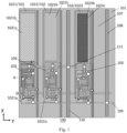
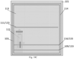
- Fig. 1 is a planar structural schematic diagram of a display substrate provided by at least one embodiment of the present disclosure, as shown in Fig. 1 , the display substrate 100 includes: a first base substrate 101 and a plurality of sub-pixels 102 on the first base substrate 101.
- the arrangement direction of the plurality of sub-pixels 102 is a second direction Y, that is, the plurality of sub-pixels 102 are arranged side by side in the second direction Y.
- the plurality of sub-pixels 102 include a first sub-pixel 1021 and a second sub-pixel 1022 arranged side by side in the second direction Y, and a direction that intersects or is perpendicular to the second direction Y is a first direction X.
- the first sub-pixel 1021 includes a first pixel circuit 1021a and a first effective light-emitting region 1021b in the first direction X; the second sub-pixel 1022 includes a second pixel circuit 1022a and a second effective light-emitting region 1022b in the first direction X.
- a first light-shielding layer 103 is provided between the first pixel circuit 1021a and the first base substrate 101, and an orthographic projection of the first light-shielding layer 103 on the first base substrate 101 at least partially overlaps with an orthographic projection of the first pixel circuit 1021a on the first base substrate 101.
- a second light-shielding layer 104 is provided between the second pixel circuit 1022a and the first base substrate 101, and an orthographic projection of the second light-shielding layer 104 on the first base substrate 101 at least partially overlaps with an orthographic projection of the second pixel circuit 1022a on the first base substrate 101.
- a wavelength of light emitted from the first effective light-emitting region 1021b is greater than a wavelength of light emitted from the second effective light-emitting region 1022b
- the ratio of the area of the first light-shielding layer 103 to the area of the first sub-pixel 1021 is a
- the ratio of the area of the second light-shielding layer 104 to the area of the second sub-pixel 1022 is b
- the ratio M1 of a to b ranges from 1.020 to 1.120.
- the ratio M1 of a to b is less than 1.020, the ratio a of the area of the first light-shielding layer 103 to the area of the first sub-pixel 1021 is too small, resulting in a higher opening ratio of the first sub-pixel 1021 and a lower opening ratio of the second sub-pixel 1022, which leads to poor final color mixing effect.
- the ratio M1 of a to b is greater than 1.120, the ratio a of the area of the first light-shielding layer 103 to the area of the first sub-pixel 1021 is too large, resulting in a lower opening rate of the first sub-pixel 1021 and a higher opening rate of the second sub-pixel 1022, which leads to poor final color mixing effect.
- the shielding protection effect on the first pixel circuit 1021a is relatively weak (for example, the first light-shielding layer 103 at least overlaps with the active layer of the driving transistor of the first pixel circuit 1021a to provide shielding protection and avoid leakage current caused by external light irradiation).
- the second light-shielding layer 104 corresponding to the second sub-pixel 1022 is smaller, which weakens the shielding protection effect on the second pixel circuit 1022a (for example, the first light-shielding layer 103 at least overlaps with the active layer of the driving transistor of the second pixel circuit 1022a to provide shielding protection and avoid leakage current caused by external light irradiation).
- the first sub-pixel and the second sub-pixel included in the plurality of sub-pixels may be two adjacent sub-pixels arranged side by side along the second direction in one pixel unit, or two sub-pixels arranged side by side and spaced apart from each other along the second direction in one pixel unit.
- the embodiments of the present disclosure are not limited in this aspect, as long as the first sub-pixel and the second sub-pixel are in the same pixel unit.
- the first sub-pixel 1021 and the second sub-pixel 1022 are respectively red sub-pixel and green sub-pixel, correspondingly, the first effective light-emitting region 1021b is a red light-emitting region, and the second effective light-emitting region 1022b is a green light-emitting region.
- the light-emitting region of the red sub-pixel is larger than the light-emitting region of the green sub-pixel, that is, the area of the first effective light-emitting region 1021b is larger than the area of the second effective light-emitting region 1022b, by providing the area of the first light-shielding layer 103 to be larger than the area of the second light-shielding layer 104, the opening ratio of the first sub-pixel 1021 and the second sub-pixel 1022 can be adjusted to improve the final mixing effect. Moreover, the manufacture process of the display substrate is simpler, and the display substrate has higher light-emitting efficiency.
- the red sub-pixel is more prone to diffraction, which in turn affects the pixel circuit of the same sub-pixel or other sub-pixels. Therefore, the area of the first light-shielding layer 103 is provided to be larger than the area of the second light-shielding layer 104 to decrease the diffraction of the light emitted from the red sub-pixel.
- first light-shielding layer 103 and the second light-shielding layer 104 can be formed using the same material in the same process.
- the materials of the first light-shielding layer 103 and the second light-shielding layer 104 can be metal materials with shading performance or other materials with shading performance, which is not limited by the embodiments of the present disclosure.
- the orthographic projection of the first effective light-emitting region 1021b on the first base substrate 101 does not overlap with the orthographic projection of the first light-shielding layer 103 on the first base substrate 101
- the orthographic projection of the second effective light-emitting region 1022b on the first base substrate 101 does not overlap with the orthographic projection of the second light-shielding layer 104 on the first base substrate 101.
- the display substrate is used in a display panel
- the display panel can achieve top emission, bottom emission or bidirectional emission, the embodiments of the present disclosure are not limited in this aspect.
- a is equal to the area of the first light-shielding layer/the area of the first sub-pixel
- b is equal to the area of the second light-shielding layer/the area of the second sub-pixel
- M1 a/b.
- the area of the first sub-pixel 1021 is equal to the area of the second sub-pixel 1022, and on a plane parallel to the main surface of the first base substrate 101, the ratio of the area of the first light-shielding layer 103 to the area of the second light-shielding layer 104 is equal to M1.
- the region shielded by the first light-shielding layer 103 is not an opening region, and in addition to the region shielded by the first light-shielding layer 103 and the opening region, the first sub-pixel 1021 also includes other regions.
- the region shielded by the second light-shielding layer 104 is not an opening region, and in addition to the region shielded by the second light-shielding layer 104 and the opening region, the second sub-pixel 1022 also includes other regions.
- the opening ratio of the first sub-pixel 1021 is n1 (1-a), where n1 is the ratio of the area of the opening region in the first sub-pixel 1021 to the area of the portion in the first sub-pixel 1021 other than the region shielded by the first light-shielding layer 103.
- the opening ratio of the second sub-pixel is n2 (1-b), where n2 is the ratio of the area of the opening region in the second sub-pixel 1022 to the area of the portion in the second sub-pixel 1022 other than the region shielded by the second light-shielding layer 104.
- the initial brightness of the first sub-pixel is 26.1cd/m 2
- the initial brightness of the second sub-pixel is 86.1cd/m 2
- the luminescence lifetime of the first sub-pixel is 150000 hours
- the luminescence lifetime of the second sub-pixel is 40000 hours
- n2 n1
- the initial brightness can be obtained by testing the brightness of each sub-pixel in a display device under a certain grayscale condition.
- the wavelength of the light emitted by the second sub-pixel is shorter, the initial brightness of the second sub-pixel is higher, and the lifetime is shorter; the wavelength of the light emitted by the first sub-pixel is longer, the initial brightness of the first sub-pixel is lower, and the lifetime is longer. Therefore, it can be obtained that K1 is smaller than K2.
- the first sub-pixel is a red sub-pixel
- the second sub-pixel is a green sub-pixel.
- the initial brightness of the green sub-pixel is higher, and the lifetime of the green sub-pixel is shorter.
- the initial brightness of the red sub-pixel is lower, and the lifetime of the red sub-pixel is longer. Therefore, K1 is smaller than K2.
- the plurality of sub-pixels 102 further include a third sub-pixel 1023, that is, the third sub-pixel 1023 is further provided on the first base substrate 101 and the third sub-pixel 1023 is arranged side by side with the first sub-pixel 1021 and the second sub-pixel 1022.
- the third sub-pixel 1023 may include a third pixel circuit 1023a and a third effective light-emitting region 1023b.
- a third light-shielding layer 105 is provided between the third pixel circuit 1023a and the first base substrate 101, and an orthographic projection of the third light-shielding layer 105 on the first base substrate 101 at least partially overlaps with an orthographic projection of the third pixel circuit 1023a on the first base substrate 101.
- the wavelength of the light emitted from the third effective light-emitting region 1023b is smaller than the wavelength of the light emitted from the second effective light-emitting region 1022b, and on a plane parallel to the main surface of the first base substrate 101, an area ratio c of the third light-shielding layer 105 is equal to a ratio of the area of the third light-shielding layer 105 to the area of the third sub-pixel 1023, and the opening ratio of the third sub-pixel 1023 is n3 (1-c).
- the first effective light-emitting region 1021b, the second effective light-emitting region 1022b, and the third effective light-emitting region 1023b respectively correspond to the red light-emitting region, the green light-emitting region, and the blue light-emitting region, and correspondingly, the first sub-pixel 1021, the second sub-pixel 1022, and the third sub-pixel 1023 are respectively the red sub-pixel, the green sub-pixel, and the blue sub-pixel.
- the initial brightness of the second sub-pixel 1022 is 86.1cd/m 2
- the luminescence lifetime of the second sub-pixel 1022 is 40000 hours
- the initial brightness of the third sub-pixel 1023 is 11.3cd/m 2
- the luminescence lifetime of the third sub-pixel 1023 is 60000 hours
- the first sub-pixel 1021 further includes a first light-emitting element 1021c, the first pixel circuit 1021a controls the first light-emitting element 1021c to emit light, and the color of the light emitted by the first light-emitting element 1021c is the same as the color of the light emitted from the first effective light-emitting region 1021b.
- the second sub-pixel 1022 further includes a second light-emitting element 1022c, and the second pixel circuit 1022a controls the second light-emitting element 1022c to emit light, and the color of the light emitted by the second light-emitting element 1022c is the same as the color of the light emitted from the second effective light-emitting region 1022b.
- the third sub-pixel 1023 further includes a third light-emitting element 1023c, and the third pixel circuit 1023a controls the third light-emitting element 1023c to emit light, and the color of the light emitted by the third light-emitting element 1023c is the same as the color of the light emitted from the third effective light-emitting region 1023b.
- the first emitting element 1021c, the second emitting element 1022c, and the third emitting element 1023c respectively emit first color light, second color light, and third color light, and the first color light, the second color light, and the third color light can be mixed to form white light.
- the first emitting element, the second emitting element, and the third emitting element respectively emit red light, green light, and blue light.
- the area of the first light-shielding layer 103: the area of the second light-shielding layer 104: the area of the third light-shielding layer 105 20:19:18.
- the longer the wavelength the more likely diffraction occurs, which in turn affects the pixel circuit of the same sub-pixel or other sub-pixels. Therefore, sub-pixels with longer wavelengths correspond to larger light-shielding layers, to slow down the diffraction effect of the emitted light.
- a: b: c 20:19:18.
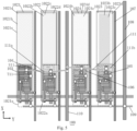
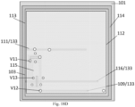
- Fig. 2 is a planar structural schematic diagram of another display substrate provided by at least one embodiment of the present disclosure, as shown in Fig. 2 , compared to the structure of the display substrate shown in Fig. 1 , in the structure shown in Fig. 2 , the plurality of sub-pixels 102 further include a fourth sub-pixel 1024, that is, the fourth sub-pixel 1024 is further provided on the first base substrate 101 and arranged side by side with the first sub-pixel 1021, the second sub-pixel 1022, and the third sub-pixel 1023.
- the fourth sub-pixel 1024 is further provided on the first base substrate 101 and arranged side by side with the first sub-pixel 1021, the second sub-pixel 1022, and the third sub-pixel 1023.
- the first sub-pixel 1021, the second sub-pixel 1022, the fourth sub-pixel 1024, and the third sub-pixel 1023 are arranged side by side, the embodiments of the present disclosure are not limited to this.
- the third sub-pixel 1023 may also be provided between the second sub-pixel 1022 and the fourth sub-pixel 1024 or arranged in other order, which is not limited by the embodiments of the present disclosure.
- first sub-pixel 1021 the relevant features of the first sub-pixel 1021, the second sub-pixel 1022, and the third sub-pixel 1023 can be referred to the above descriptions of Fig. 1 .
- the fourth sub-pixel 1024 includes a fourth pixel circuit 1024a and a fourth effective light-emitting region 1024b.
- a fourth light-shielding layer 106 is provided between the fourth pixel circuit 1024a and the first base substrate 101, and an orthographic projection of the fourth light-shielding layer 106 on the first base substrate 101 at least partially overlaps with an orthographic projection of the fourth pixel circuit 1024a on the first base substrate 101.
- the wavelength of the light emitted from the fourth effective light-emitting region 1024b is greater than the wavelength of the light emitted from the second effective light-emitting region 1022b, and on a plane parallel to the main surface of the first base substrate 101, the area ratio d of the fourth light-shielding layer 106 is equal to the ratio of the area of the fourth light-shielding layer 106 to the area of the fourth sub-pixel 1024.
- the opening ratio n4 (1-d) of the fourth sub-pixel 1024 ranges from 0.230 to 0.950, where n4 is the ratio of the area of the opening region in the fourth sub-pixel to the area of the portion in the fourth sub-pixel other than the region shielded by the fourth light-shielding layer.
- the light emitted from the fourth sub-pixel 1024 is white light, that is, the fourth sub-pixel 1024 is a white sub-pixel, and correspondingly, the fourth effective light-emitting region 1024b is a white light-emitting region.
- Fig. 3 is a planar structural schematic diagram of further another display substrate provided by at least one embodiment of the present disclosure, as shown in Fig. 3 , the first sub-pixel 1021 includes a first light-emitting element 1021c, and the first pixel circuit 1021a controls the first light-emitting element 1021c to emit light.
- the second sub-pixel 1022 also includes a second light-emitting element 1022c, and the second pixel circuit 1022a controls the second light-emitting element 1022c to emit light.
- the third sub-pixel 1023 also includes a third light-emitting element 1023c, and the third pixel circuit 1023a controls the third light-emitting element 1023c to emit light.
- the fourth sub-pixel 1024 also includes a fourth light-emitting element 1024c, and the fourth pixel circuit 1024a controls the fourth light-emitting element 1024c to emit light.
- the first emitting element 1021c, the second emitting element 1022c, the third emitting element 1023c, and the fourth emitting element 1024c are all white emitting elements, and a first filter layer 1021d, a second filter layer 1022d, a third filter layer 1023d, and a light transmitting layer 1024d are respectively provided on the sides of the first emitting element 1021c, the second emitting element 1022c, the third emitting element 1023c, and the fourth emitting element 1024c away from the first base substrate 101.
- the color of the light emitted from the first filter layer 1021d is the same as the color of the light emitted from the first effective light-emitting region 1021b
- the color of the light emitted from the second filter layer 1022d is the same as the color of the light emitted from the second effective light-emitting region 1022b
- the color of the light emitted from the third filter layer 1023d is the same as the color of the light emitted from the third effective light-emitting region 1023b
- the color of the light emitted from the light transmitting layer 1024d is the same as the color of the light emitted from the fourth effective light-emitting region 1024b, which is still white light.
- the first base substrate 101 has been omitted in Fig. 3 .
- the transmittance of the material of the first filter layer 1021d is ⁇ 1
- the transmittance of the material of the second filter layer 1022d is ⁇ 2
- the transmittance of the material of the third filter layer 1023d is ⁇ 3
- the transmittance of the material of the light transmitting layer 1024d is ⁇ 4.
- the first light-emitting element 1021c, the second light-emitting element 1022c, the third light-emitting element 1023c, and the fourth light-emitting element 1024c are all light-emitting elements that emit white light.
- This design can improve the uniformity of the emitted light, and the white light can adjust the width of the spectrum, and perform optical compensation.
- the ratio of the total of an area of the first filter layer 1021d, an area of the second filter layer 1022d, an area of the third filter layer 1023d, and an area of the light transmitting layer 1024d to the total of an area of the first light-shielding layer 103, an area of the second light-shielding layer 104, an area of the third light-shielding layer 105, and an area of the fourth light-shielding layer 106 ranges from 1.050 to 6.800, for example, the ratio may be 1.100, 1.200, 2.000, 2.500, 3.000, 3.500, 4.000, 4.500, 5.000, 5.500, 6.000, 6.500, which is not limited by the embodiments of the present disclosure.
- the ratio of the total area of the first filter layer 1021d, the second filter layer 1022d, the third filter layer 1023d, and the light transmitting layer 1024d to the total area of the first light-shielding layer 103, the second light-shielding layer 104, the third light-shielding layer 105, and the fourth light-shielding layer 106 ranges from 1.100 to 3.300.
- the ratio may be 1.200, 1.300, 1.400, 1.600, 1.800, 2.000, 2.400, 2.700, 2.900, 3.100, 3.200, or 3.300, which is not limited by the embodiments of the present disclosure.
- the ratio of the area of the first filter layer 1021d to the area of the first light-shielding layer 103 ranges from 2.000 to 3.000, for example, the ratio is 2.000, 2.200, 2.400, 2.600, 2.800, or 3.000.
- the ratio of the area of the second filter layer 1022d to the area of the second light-shielding layer 104 ranges from 1.1074 to 1.6938.
- the ratio of the area of the second filter layer 1022d to the area of the second light-shielding layer 104 is 1.1074, 1.200, 1.300, 1.400, 1.500 or 1.600, which is not limited by the embodiments of the present disclosure.
- the ratio of the area of the third filter layer 1023d to the area of the third light-shielding layer 105 ranges from 1.4650 to 2.02268.
- the ratio of the area of the third filter layer 1023d to the area of the third light-shielding layer 105 is 1.510, 1.600, 1.700, 1.800, 1.900, or 2.100, which is not limited by the embodiments of the present disclosure.
- the ratio of the area of the light transmitting layer 1024d to the area of the fourth light-shielding layer 106 ranges from 2.1760 to 3.2850.
- the ratio of the area of the light transmitting layer 1024d to the area of the fourth light-shielding layer 106 is 2.210, 2.600, 2.700, 2.800, 2.900, or 3.100, which is not limited by the embodiments of the present disclosure.
- the display substrate 100 further includes a data line 107 and a first sensing line 108 that extend along the first direction X, and a second sensing line 109 that extends along the second direction Y.
- the data line 107 intersects with the second sensing line 109 to define a plurality of pixel regions, and each pixel region includes one sub-pixel 102.
- a first power voltage line 110 parallel to the data line 107 is provided between adjacent sub-pixels 102, and a second power voltage line 111 parallel to the second direction Y is provided on a side of the first effective light-emitting region 1021b close to the first light-shielding layer 103.
- the second power voltage line 111 intersects with the first power voltage line 110 and is connected to the first drain electrode of the first driving transistor in the first pixel circuit 1021a, the orthographic projection of the second power voltage line 111 on the first base substrate 101 overlaps with the orthographic projection of the first light-shielding layer 103 on the first base substrate 101.
- the orthographic projection of the second power voltage line 111 on the first base substrate 101 and the orthographic projection of the first light-shielding layer 103 on the first base substrate 101 have an overlapping portion.
- the orthographic projection of the second power voltage line 111 on the first base substrate 101 does not have an overlapping portion with all of the orthographic projection of the second light-shielding layer 104 on the first base substrate 101, the orthographic projection of the third light-shielding layer 105 on the first base substrate 101, and the orthographic projection of the fourth light-shielding layer 106 on the first base substrate 101, however, the orthographic projection of the second power voltage line 111 on the first base substrate 101 and the orthographic projection of the fourth light-shielding layer 106 on the first base substrate 101 have adjacent portions.
- This design can enhance the stability of the first light-shielding layer 103, and a capacitor can be formed between the first light-shielding layer 103 and the second power voltage line 111, thereby avoiding drift of the first light-shielding layer 103 when the gate signal is not turned on.
- the orthographic projection of the second power voltage line 111 on the first base substrate 101 and the orthographic projection of the first light-shielding layer 103 on the first base substrate 101 have an overlapping portion, and the orthographic projection of the second power voltage line 111 on the first base substrate 101 does not have an overlapping portion with the orthographic projection of the second light-shielding layer 104 on the first base substrate 101, and the orthographic projection of the third light-shielding layer 105 on the first base substrate 101.
- the orthographic projection of the second power voltage line 111 on the first base substrate 101 does not have an overlapping portion with all of and the orthographic projection of the first light-shielding layer 103 on the first base substrate 101, the orthographic projection of the second light-shielding layer 104 on the first base substrate 101, the orthographic projection of the third light-shielding layer 105 on the first base substrate 101, and the orthographic projection of the fourth light-shielding layer 106 on the first base substrate 101.
- the second sensing line 109 extending along the second direction Y may extend in a curve line, a broken line, or a straight line, as long as the overall extension direction of the second sensing line 109 is along the second direction Y.
- the second sensing line 109 extends along a straight line.
- the second power voltage line 111 is connected to the source electrode S11 of the driving transistor T11 in the first sub-pixel 1021, the second power voltage line 111 is connected to the source electrode S12 of the driving transistor T12 in the second sub-pixel 1022, the second power voltage line 111 is connected to the source electrode S13 of the driving transistor T13 in the third sub-pixel 1023, and the second power voltage line 111 is connected to the source electrode S14 of the driving transistor T14 in the fourth sub-pixel 1024.
- the orthographic projection of the second power voltage line 111 on the first base substrate 101 overlaps with the orthographic projection of the first light-shielding layer 103 on the first base substrate 101, and overlaps with the orthographic projection of the fourth light-shielding layer 106 on the first base substrate 101, the orthographic projection of the second power voltage line 111 on the first base substrate 101 does not have an overlapping portion with the orthographic projection of the second light-shielding layer 104 on the first base substrate 101, and the orthographic projection of the third light-shielding layer 105 on the first base substrate 101.
- This design can enhance the stability of the first light-shielding layer 103 and the fourth light-shielding layer 106, capacitors can be formed between the first light-shielding layer 103 and the second power supply voltage line 111, as well as between the fourth light-shielding layer 106 and the second power voltage line 111, thereby avoiding drift of the first light-shielding layer 103 and the fourth light-shielding layer 106 when the gate signal is not turned on.
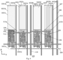
- Fig. 4 is a planar structural schematic diagram of further another display substrate provided by at least one embodiment of the present disclosure, as shown in Fig. 4 , the orthographic projection of the second power voltage line 111 on the first base substrate 101 has an overlapping portion with all of the orthographic projection of the first light-shielding layer 103 on the first base substrate 101, the orthographic projection of the second light-shielding layer 104 on the first base substrate 101, the orthographic projection of the third light-shielding layer 105 on the first base substrate 101, and the orthographic projection of the fourth light-shielding layer 106 on the first base substrate 101.
- the overlapping area of the orthographic projection of the second power voltage line 111 on the first base substrate 101 and the orthographic projection of the first light-shielding layer 103 on the first base substrate 101 is greater than the overlapping area of the orthographic projection of the second power voltage line 111 on the first base substrate 101 and the orthographic projection of the second light-shielding layer 104 on the first base substrate 101, and the capacitance value between the first light-shielding layer 103 and the second power voltage line 111, and the capacitance value between the fourth light-shielding layer 106 and the second power voltage line 111 are balanced.
- the overlapping area of the orthographic projection of the second power voltage line 111 on the first base substrate 101 and the orthographic projection of the first light-shielding layer 103 on the first base substrate 101 is greater than the overlapping area of the orthographic projection of the second power voltage line 111 on the first base substrate 101 and the orthographic projection of the third light-shielding layer 105 on the first base substrate 101.
- This design can enhance the stability of the first light-shielding layer 103 and the third light-shielding layer 105, and balance the capacitance value between the first light-shielding layer 103 and the second power voltage line 111, and the capacitance value between the third light-shielding layer 105 and the second power voltage line 111.
- the overlapping area of the orthographic projection of the second power voltage line 111 on the first base substrate 101 and the orthographic projection of the first light-shielding layer 103 on the first base substrate 101 is greater than the overlapping area of the orthographic projection of the second power voltage line 111 on the first base substrate 101 and the orthographic projection of the fourth light-shielding layer 106 on the first base substrate 101.
- the overlapping area of the orthographic projection of the second power voltage line 111 on the first base substrate 101 and the orthographic projection of the fourth light-shielding layer 106 on the first base substrate 101 is greater than the overlapping area of the orthographic projection of the second power voltage line 111 on the first base substrate 101 and the orthographic projection of the third light-shielding layer 105 on the first base substrate 101.
- the overlapping area of the orthographic projection of the second power voltage line 111 on the first base substrate 101 and the orthographic projection of the third light-shielding layer 105 on the first base substrate 101 is greater than the overlapping area of the orthographic projection of the second power voltage line 111 on the first base substrate 101 and the orthographic projection of the second light-shielding layer 104 on the first base substrate 101.
- This design can enhance the stability of the first light-shielding layer 103, the second light-shielding layer 104, the third light-shielding layer 105, and the fourth light-shielding layer 106, and balance the capacitance value between the first light-shielding layer 103 and the second power voltage line 111, the capacitance value between the second light-shielding layer 104 and the second power voltage line 111, the capacitance value between the third light-shielding layer 106 and the second power voltage line 111, and the capacitance value between the fourth light-shielding layer 106 and the second power voltage line 111.
- the overlapping area of the orthographic projection of the second power voltage line 111 on the first base substrate 101 and the orthographic projection of the first light-shielding layer 103 on the first base substrate 101 ranges from 0.03 square micrometers to 0.30 square micrometers.
- the overlapping area of the orthographic projection of the second power voltage line 111 on the first base substrate 101 and the orthographic projection of the fourth light-shielding layer 106 on the first base substrate 101 ranges from 0.02 square micrometers to 0.20 square micrometers.
- the overlapping area of the orthographic projection of the second power voltage line 111 on the first base substrate 101 and the orthographic projection of the third light-shielding layer 105 on the first base substrate 101 ranges from 0 to 0.05 square micrometers
- the overlapping area of the orthographic projection of the second power voltage line 111 on the first base substrate 101 and the orthographic projection of the second light-shielding layer 104 on the first base substrate 101 ranges from 0 to 0.08 square micrometers.
- the second power voltage line 111 extending along the second direction Y may extend in a curve line, a broken line, or a straight line, as long as the overall extension direction of the second power voltage line 111 is along the second direction Y.
- the second power voltage line 111 extends along a straight line.
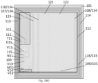
- Fig. 5 is a planar structural schematic diagram of further another display substrate provided by at least one embodiment of the present disclosure, as shown in Fig. 5 , the second power voltage line 111 includes a first portion 111a and a second portion 111b that are spaced apart from each other.
- the first portion 111a and the second portion 111b are connected to the first power voltage line 110 through different via structures.
- setting the second power voltage line 111 to include a plurality of portions that are spaced apart from each other and not directly connected with each other can avoid the accumulation of too much charges on the second power voltage line 111 due to the second power voltage line 111 being too long.
- both the first portion 111a and the second portion 111b extend along a curve line, but the embodiments of the present disclosure are not limited to this, both the first portion 111a and the second portion may also 111b extend along a straight line.
- the first portion 111a is connected to the first source electrode S11 of the first driving transistor T11 in the first pixel circuit 1021a, and the second source electrode S12 of the second driving transistor T12 in the second pixel circuit 1022a.
- the second portion 111b is connected to the third source electrode S13 of the third driving transistor T13 in the third pixel circuit 1023a, and the fourth source electrode S14 of the fourth driving transistor T14 in the fourth pixel circuit 1024a, thereby balancing the accumulated charges on the first portion 111a and the second portion 111b, and making the charges more dispersed.
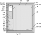
- Fig. 6 is a planar structural schematic diagram of further another display substrate provided by at least one embodiment of the present disclosure, as shown in Fig. 6 , the extension direction of the first portion 111a is parallel to the extension direction of the second portion 111b. Both the first portion 111a and the second portion 11 1b extend along a straight line.
- the first portion 11 1a is connected to the first source electrode S11 of the first driving transistor T11 in the pixel circuit 1021a and the second source electrode S12 of the second driving transistor T12 in the second pixel circuit 1022a
- the second portion 111b is connected to the third source electrode S13 of the third driving transistor T13 in the third pixel circuit 1023a and the fourth source electrode S14 of the fourth driving transistor T14 in the fourth pixel circuit 1024a
- the first portion 111a is located on the side of the second portion 111b close to the second sensing line 109, thereby making the wiring process easier.
- the first portion 11 1a is connected to the middle region of the first source electrode S11 and the second source electrode S12, while the second portion 111b is connected to the edge of the third source electrode S13 away from the second sensing line 109 and the edge of the fourth source electrode S14 away from the second sensing line 109, which can make the display substrate more finely designed in size.
- Fig. 7 is a planar structural schematic diagram of further another display substrate provided by at least one embodiment of the present disclosure, as shown in Fig. 7 , both the first portion 111a and the second portion 111b extend along a broken line.
- the first portion 111a is connected to the edge of the first source electrode S11 away from the second sensing line 109 and the middle region of the third source electrode S13
- the second portion 111b is connected to the edge of the second source electrode S12 away from the second sensing line 109 and the middle region of the fourth source electrode S14.
- the first portion 111a and the second portion 111b are electrically connected to the first power voltage line 110 through the same via structure.
- the first portion 111a and the second portion 111b both extend along a broken line, and therefore the connection positions of the second power voltage line 111 and the first source electrode S11, the second source electrode S12, the third source electrode S13, and the fourth source electrode S14 can be flexibly adjusted according to the circuit design situation.
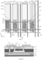
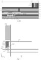
- Fig. 8A is a cross-sectional structural schematic diagram of the display substrate in Fig. 1 to Fig. 3 along a line A-A', as shown in Fig. 8A , the first drain electrode D11 and the first light-shielding layer 103 are connected through a first via V11, the first via V11 sequentially penetrates the interlayer insulation layer 112, the gate insulation layer 113, and the buffer layer 114. As shown in Fig. 8A , the first drain electrode D11 and the active layer 115 are connected through a second via V12, and the first source electrode S11 and the active layer 115 are connected through a second via V12, the second via V12 sequentially penetrates the interlayer insulation layer 112 and the gate insulation layer 113.
- the gate electrode G11 is on the side of the active layer 115 away from the first base substrate 101.
- the embodiments of the present disclosure are not limited to this, the gate electrode G11 may also be provided on the side of the active layer 115 close to the first base substrate 101.
- Fig. 8B is a cross-sectional structural schematic diagram of the display substrate in Fig. 4 along a line B-B' and a line C-C', as shown in Fig. 8B , a passivation layer 121 and a planarization layer 122 are provided on the side of the first drain electrode D11 and the first source electrode S11 away from the first base substrate 101, and a first electrode 123 is provided on the side of the planarization layer 122 away from the first base substrate 101.
- the first electrode 123 may be an anode, and is connected to the first drain electrode D11.
- a first color light-emitting unit 1021e, a second color light-emitting unit 1022e, a third color light-emitting unit 1023e, and a fourth color light-emitting unit 1024e are arranged side by side.
- the first color light-emitting unit 1021e, the second color light-emitting unit 1022e, the third color light-emitting unit 1023e, and the fourth color light-emitting unit 1024e may respectively be the red light-emitting unit, the green light-emitting unit, the blue light-emitting unit, and the white light-emitting unit.
- the first color light-emitting unit 1021e, the second color light-emitting unit 1022e, and the third color light-emitting unit 1023e may respectively be the first color light-emitting layer emitting the first color light, the second color light-emitting layer emitting the second color light, and the third color light-emitting layer emitting the third color light.
- the first color light-emitting unit 1021e, the second color light-emitting unit 1022e, the third color light-emitting unit 1023e, and the fourth color light-emitting unit 1024e may be a combination of a white light-emitting element and a first filter layer, a second filter layer, a third filter layer, and a light transmitting layer.
- the first filter layer, the second filter layer, and the third filter layer may respectively be a red filter layer, a green filter layer, and a blue filter layer.
- a second electrode is further provided on the side of the first color light-emitting unit 1021e, the second color light-emitting unit 1022e, the third color light-emitting unit 1023e, and the fourth color light-emitting unit 1024e away from the first base substrate 101, the second electrode may be a cathode.
- the other structures of the display substrate 100 can refer to conventional designs, and the embodiments of the present disclosure are not limited to this.
- the thin film transistor in the embodiments of the present disclosure may be a bottom gate thin film transistor or a top gate thin film transistor.
- Fig. 8A and Fig. 8B are illustrated using the top gate thin film transistor as an example.
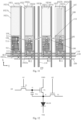
- Fig. 9 is a planar structural schematic diagram of further another display substrate provided by at least one embodiment of the present disclosure, as shown in Fig. 9 , the display substrate 100 further includes a first gate line 116 extending along the second direction Y, and a first gate electrode 117 extending from the first gate line 116 towards the side close to the second power voltage line 111.
- the planar shape of the first light-shielding layer 103 includes a first sub-portion 103a and a second sub-portion 103b extending along the first direction X.
- the first distance W1 between the first side 103a' of the first sub-portion 103a close to the first gate line 116 and the first gate line 116 is greater than the second distance W2 between the second side 103b' of the second sub-portion 103b close to the first gate electrode 117 and the first gate electrode 117.
- the area of the first sub-portion 103a is greater than the area of the second sub-portion 103b on the plane parallel to the main surface of the first base substrate 101
- the first distance W1 between the first side 103a' of the first sub-portion 103a close to the first gate line 116 and the first gate line 116 is greater than the second distance W2 between the second side 103b' of the second sub-portion 103b close to the first gate electrode 117 and the first gate electrode 117.
- the overall shape formed by the first sub-portion 103a and the second sub-portion 103b included in the first light-shielding layer 103 includes a step shape, and the step shape is located at the edge of the first light-shielding layer 103 close to the first gate line 116.
- first sub-portion 103a and the second sub-portion 103b included in the first light-shielding layer 103 may be a whole or connected through a bridging structure, the embodiments of the present disclosure are not limited to this.
- Fig. 9 shows the design in the first sub-pixel 1021
- the above structural design can also apply in the second sub-pixel, the third sub-pixel, and the fourth sub-pixel, that is, the second light-shielding layer 104, the third light-shielding layer 105, and the fourth light-shielding layer 106 all have the structure that includes two portions similar to the first light-shielding layer 103.
- Fig. 10 is a planar structural schematic diagram of further another display substrate provided by at least one embodiment of the present disclosure, as shown in Fig. 10 , the second sensing line 109 includes two portions that are spaced apart from each other, which are connected to the first sensing line 108 through different via structures.
- the first sensing line 108 is adjacent to the first power voltage line 110.
- the first sensing line 108 and the first power voltage line 110 are both provided between the second sub-pixel 1022 and the fourth sub-pixel 1024.
- setting the second sensing line 109 to include two portions that are spaced apart from each other and not directly connected with each other can avoid the accumulation of too much charges on the second sensing line 109 due to the second sensing line 109 being too long.
- the other structural designs on the display substrate 100 can be referred to in the relevant description above, and will not be repeated here.
- Fig. 11 is a planar structural schematic diagram of further another display substrate provided by at least one embodiment of the present disclosure, as shown in Fig. 11 , the display substrate 100 further includes a second gate line 118 parallel to the first gate line 116, the first gate line 117 is configured as the gate electrode of the first switching transistor N11, the second gate line 118 is configured as the gate electrode of the first sensing transistor M11 included in the first pixel circuit 1021a, the gate electrode of the second sensing transistor M12 included in the second pixel circuit 1022a, the gate electrode of the third sensing transistor M13 included in the third pixel circuit 1023a, and the gate electrode of the fourth sensing transistor M14 included in the fourth pixel circuit 1024a, the display substrate 100 includes both the first gate line 116 and the second gate line 118, such that in one sub-pixel, the switching transistor (e.g., the first switching transistor) and the corresponding sensing transistor (e.g., the first sensing transistor) are controlled by different control lines, which further makes the adjustment of the switching transistor
- the display substrates in Fig. 1 to Fig. 11 above are all organic light-emitting diode (OLED) display substrates, and the first light-emitting element, the second light-emitting element, the third light-emitting element, and the fourth light-emitting element are all OLEDs.
- the above display substrate includes a plurality of gate lines and a plurality of data lines for providing scanning signals (control signals) and data signals to drive the plurality of sub-pixels.
- the pixel circuit includes a drive sub-circuit for driving the light-emitting element to emit light and a detection sub-circuit for detecting the electrical characteristics of the sub-pixel to achieve external compensation.
- the specific structure of the pixel circuit is not limited by the embodiments of the present disclosure.
- Fig. 12 is a schematic diagram of a 3T1C pixel circuit for a display substrate provided by at least one embodiment of the present disclosure, as needed, the pixel circuit may further include a compensation circuit and a reset circuit, etc.
- the embodiments of the present disclosure are not limited to this.
- the pixel circuit includes a first transistor T1, a second transistor T2, a third transistor T3, and a storage capacitor Cst.
- the first transistor T1 may be a driving transistor
- the second transistor T2 may be a switching transistor
- the third transistor T3 may be a sensing transistor
- the first electrode of the second transistor T2 is electrically connected to the first capacitor electrode of the storage capacitor Cst and the gate electrode of the first transistor T1
- the second electrode of the second transistor T2 is configured to receive the data signal GT
- the second transistor T2 is configured to write the data signal DT into the gate electrode of the first transistor T1 and the storage capacitor Cst in response to the first control signal G1.
- the first electrode of the first transistor T1 is electrically connected to the second capacitor electrode of the storage capacitor Cst, and is configured to be electrically connected to the first electrode of the light-emitting element.
- the second electrode of the first transistor T1 is configured to receive a first power voltage V1 (such as a high power voltage VDD), and the first transistor T1 is configured to control the current used to drive the light-emitting element under the control of the gate voltage of the first transistor T1;
- the first electrode of the third transistor T3 is electrically connected to the first electrode of the first transistor T1 and the second capacitor electrode of the storage capacitor Cst, the second electrode of the third transistor T3 is configured to be connected to the first detection line to be connected to the external detection circuit, and the third transistor T3 is configured to detect the electrical characteristics of the sub-pixel to which it belongs in response to the second control signal G2 to achieve external compensation; the electrical characteristics include, for example, the threshold voltage and/or carrier mobility of the first transistor T1, or the threshold voltage and driving current of the light-emitting
- the transistors used in the embodiments of the present disclosure may all be thin film transistors, field-effect transistors, or other switching devices with the same characteristics.
- the above transistors being thin film transistors are used as examples to illustrate.
- the source electrode and the drain electrode of the transistor used here may be symmetrical in structure, so the source electrode and the drain electrode can be structurally indistinguishable.
- the transistors can be divided into N-type transistors and P-type transistors.
- the turn-on voltage is a low-level voltage (such as 0V, -5V, -10V or other suitable voltage), and the turn-off voltage is a high-level voltage (such as 5V, 10V or other suitable voltage);
- the turn-on voltage is a high-level voltage (e.g. 5V, 10V or other suitable voltage)
- the turn-off voltage is a low-level voltage (e.g. 0V, -5V, -10V or other suitable voltage).
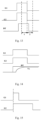
- Fig. 12 The working principle of the pixel circuit shown in Fig. 12 is illustrated by combining the signal timing diagrams shown in Fig. 13 to Fig. 15 , in which Fig. 13 is a signal timing diagram of the pixel circuit in Fig. 12 during a display process, Fig. 14 is a first signal timing diagram of the pixel circuit in Fig. 12 during a detection process, and Fig. 15 is a second signal timing diagram of the pixel circuit in Fig. 12 during a detection process.
- the display process of each frame of the image includes a data writing and resetting stage 1 and a light-emitting stage 2.
- Fig. 13 shows the timing waveform of each signal in each stage.
- One operating process of the 3T1C pixel circuit includes: in the data writing and resetting stage 1, the first control signal G1 and the second control signal G2 are both turn-on signals, the second transistor T2 and the third transistor T3 are turned on, and the data signal DT is transmitted to the gate electrode of the first transistor T1 through the second transistor T2, the analog-to-digital converter writes a reset signal to the first electrode of the light-emitting element (such as the anode of an OLED) through the third transistor T3.
- the first control signal G1 and the second control signal G2 are both turn-on signals
- the second transistor T2 and the third transistor T3 are turned on
- the data signal DT is transmitted to the gate electrode of the first transistor T1 through the second transistor T2
- the analog-to-digital converter writes a reset signal to
- the first transistor T1 is turned on and generates a driving current to charge the first electrode of the light-emitting element to the working voltage; in the light-emitting stage 2, the first control signal G1 and the second control signal G2 are both turn-off signals. Due to the bootstrap effect of the storage capacitor Cst, the voltages at both ends of the storage capacitor Cst remain unchanged, the first transistor T1 operates in a saturated state with constant current and drives the light-emitting element to emit light.
- Fig. 14 shows the signal timing diagram of the pixel circuit when detecting the threshold voltage.
- One operating process of the 3T1C pixel circuit includes: the first control signal G1 and the second control signal G2 are both turn-on signals, the second transistor T2 and the third transistor T3 are turned on, and the data signal DT is transmitted to the gate electrode of the first transistor T1 through the second transistor T2; the analog-to-digital converter writes a reset signal to the first electrode (node S) of the light-emitting element through the detection line connected to the third transistor T3 and the third transistor T3.
- the first transistor T1 is turned on and charges the node S until the first transistor T1 is turned off.
- the threshold voltage of the first transistor T1 can be obtained by sampling the voltage on the detection line through the analog-to-digital converter, this process can be carried out, for example, when the display device formed by the display substrate is in a shutdown state.
- Fig. 15 shows the signal timing diagram of the pixel circuit when detecting threshold voltage.
- One operating process of the 3T1C pixel circuit includes: in the first stage, the first control signal G1 and the second control signal G2 are both turn-on signals, the second transistor T2 and the third transistor T3 are turned on, and the data signal DT is transmitted to the gate electrode of the first transistor T1 through the second transistor T2; the analog-to-digital converter writes a reset signal to the first electrode (node S) of the light-emitting element through the detection line connected to the third transistor T3 and the third transistor T3; in the second stage, the first control signal G1 is the turn-off signal, the second control signal G1 is the turn-on signal, the second transistor T2 is turned off, the third transistor T3 is turned on, and the detection line connected to the third transistor T3 is floating.
- the first transistor T1 works in a saturated state with constant current and drives the light-emitting element to emit light, then, the analog-to-digital converter samples the voltage on the detection line and combines it with the magnitude of the light-emitting current to calculate the carrier mobility in the first transistor T1. For example, this process can be carried out during the hidden stage between display stages.
- the electrical characteristics of the first transistor T1 can be obtained and the corresponding compensation algorithm can be implemented.
- first control signal G1 and the second control signal G2 may not be turn-on signals at the same time.
- one operating process of the 3T1C pixel circuit includes: in the first stage, the first control signal G1 is the turn-on signal before the second control signal G2.
- the display substrate 100 may further include a data driving circuit and a scanning driving circuit.
- the data driving circuit is configured to output data signals as needed (such as input image signals from a display device including a display substrate), such as the above data signal DT.
- the pixel circuit of each sub-pixel is further configured to receive the data signal and apply the data signal to the gate electrode of the first transistor.
- the scanning driving circuit is configured to output various scanning signals, such as the first control signal G1 and the second control signal G2, the scanning driving circuit may be an integrated circuit chip (IC) or a gate drive circuit (GOA) directly prepared on display substrates.
- IC integrated circuit chip
- GOA gate drive circuit
- the display substrate 100 further includes a control circuit.
- the control circuit is configured to control the data driving circuit to apply data signals, and to control the gate driving circuit to apply scanning signals.
- An example of the control circuit is a timing control circuit (T-con).
- the control circuit may be various forms, such as including a processor and a memory.
- the memory includes executable codes, and the processor runs the executable codes to execute the above detection method.
- the processor may be a central processing unit (CPU) or other form of processing device with data processing and/or instruction execution capabilities, such as a microprocessor, a programmable logic controller (PLC), etc.
- CPU central processing unit
- PLC programmable logic controller
- the storage device may include one or more computer program products, which may include various forms of computer-readable storage media, such as volatile memory and/or non-volatile memory.
- the volatile memory may include, for example, random access memory (RAM) and/or cache memory.
- the non-volatile memory may include, for example, read-only memory (ROM), hard drives, flash memory, etc.
- One or more computer program instructions can be stored on the computer-readable storage medium, and the processor can perform the expected function of the program instructions.
- various applications and data can also be stored, such as electrical characteristic parameters obtained in the above detection methods.
- Fig. 16 is a cross-sectional structural schematic diagram of a display device provided by at least one embodiment of the present disclosure, as shown in Fig. 16 , the display device 20 includes the display substrate 100 in any one of the above embodiments and a cover plate 300 opposite to the display substrate 100.
- the cover plate 300 includes a second base substrate 301, and a quantum dot layer 302 is provided on a side of the second base substrate 301 close to the display substrate 100.
- the quantum dot layer 302 includes a plurality of quantum dot units 3021, which correspond to the plurality of sub-pixels in one-to-one correspondence, the color of each of the plurality of quantum dot units 3021 is the same as the color of the corresponding sub-pixel, the plurality of quantum dot units 3021 can increase the color gamut of the display device 20.
- the plurality of quantum dot units 3021 include a first quantum dot unit, a second quantum dot unit, and a third quantum dot unit.
- the color of the first quantum dot unit is the same as the color of the first sub-pixel
- the color of the second quantum dot unit is the same as the color of the second sub-pixel
- the color of the third quantum dot unit is the same as the color of the third sub-pixel.
- the first sub-pixel, the second sub-pixel, and the third sub-pixel are respectively the red sub-pixel, the green sub-pixel, and the blue sub-pixel.
- the first quantum dot unit, the second quantum dot unit, and the third quantum dot unit are respectively the red quantum dot unit, the green quantum dot unit, and the blue quantum dot unit.
- the plurality of quantum dot units 3021 include a first quantum dot unit, a second quantum dot unit, a third quantum dot unit, and a fourth quantum dot unit.
- the color of the first quantum dot unit is the same as the color of the first sub-pixel
- the color of the second quantum dot unit is the same as the color of the second sub-pixel
- the color of the third quantum dot unit is the same as the color of the third sub-pixel
- the color of the fourth quantum dot unit is the same as the color of the fourth sub-pixel.
- the first sub-pixel, the second sub-pixel, the third sub-pixel, and the fourth sub-pixel are respectively the red sub-pixel, the green sub-pixel, the blue sub-pixel, and the white sub-pixel.
- the first quantum dot unit, the second quantum dot unit, the third quantum dot unit, and the fourth quantum dot unit are respectively the red quantum dot unit, the green quantum dot unit, the blue quantum dot unit, and the white quantum dot unit.
- Fig. 16 illustrates the correspondence between the first sub-pixel and the first quantum dot unit.
- a passivation layer 121 and a planarization layer 122 are provided on the side of the first drain electrode D11 and the first source electrode S11 away from the first base substrate 101, and a first electrode 123 is provided on the side of the planarization layer 122 away from the first base substrate 101.
- the first electrode 123 may be an anode, and is connected to the first drain electrode D11.
- a pixel definition layer 124 is provided on the side of the first electrode 123 away from the first base substrate 101, and a first color light-emitting unit 1021e is provided on the side of the pixel definition layer 124 away from the first base substrate 101.
- the first color light-emitting unit 1021e is the first color light-emitting layer
- a second electrode 126 is provided on the side of the first color light-emitting unit 1021e away from the first base substrate 101, the second electrode 126 may be a cathode.
- the first color light-emitting unit 1021e, the second color light-emitting unit 1022e, and the third color light-emitting unit 1023e may be a combination of a white light-emitting element and a first filter layer, a second filter layer, and a third filter layer.
- the first filter layer, the second filter layer, and the third filter layer may be a red filter layer, a green filter layer, and a blue filter layer, respectively.
- the embodiments of the present disclosure are not limited herein.
- the first color light-emitting unit 1021e, the second color light-emitting unit 1022e, the third color light-emitting unit 1023e, and the fourth color light-emitting unit 1024e may be a combination of a white light-emitting element and a first filter layer, a second filter layer, a third filter layer, and a light transmitting layer.
- the first filter layer, the second filter layer, and the third filter layer may be a red filter layer, a green filter layer, and a blue filter layer, respectively.
- the embodiments of the present disclosure are not limited herein.
- the first drain electrode D11 and the first light-shielding layer 103 are connected through a first via V11, which sequentially penetrates the interlayer insulation layer 112 and the buffer layer 114.
- the first drain electrode D11 and the active layer 115 are connected through a second via V12, and the first source electrode S11 and the active layer 115 are connected through the second via V12, the second via V12 penetrates the interlayer insulation layer 112.
- the gate electrode G11 is provided on the side of the active layer 115 away from the first base substrate 101.
- the thin film transistors in the embodiments of the present disclosure may be bottom gate type thin film transistors or top gate type thin film transistors.
- the accompanying drawings of the embodiments of the present disclosure illustrate the thin film transistors being the top gate type thin film transistors as an example.
- the pixel definition layer 124 includes a plurality of openings, and each of the openings of the pixel definition layer 124 corresponds to the opening region of each sub-pixel of the display device 20 in one-to-one correspondence.
- the first color light-emitting unit 1021e covers the pixel definition layer 124 and the plurality of openings of the pixel definition layer 124. As shown in Fig. 16 , the portion of the first color light-emitting unit 1021e located in the plurality of openings of the pixel definition layer 124 is in contact with the first electrode 123 (anode), while the portion of the first color light-emitting unit 1021e covering the pixel definition layer 124 is not in contact with the first electrode 123 (anode).
- the portion of the first color light-emitting unit 1021e that is not in contact with the pixel definition layer 124 emits light, and the portion of the first color light-emitting unit 1021e covering the pixel definition layer 124 does not emit light.
- the first color light-emitting unit 1021e is the first color light-emitting layer.
- the first color light-emitting unit 1021e includes one or more layers of an electron transport layer (ETL), an electron injection layer (EIL), a hole transport layer (HTL), and a hole injection layer (HIL) in addition to the first color light-emitting layer.
- ETL electron transport layer
- EIL electron injection layer
- HTL hole transport layer
- HIL hole injection layer
- the display substrate 100 further includes a first thin film encapsulation layer 129 and a second thin film encapsulation layer 127.
- the second thin film encapsulation layer 127 covers the side of the second electrode 126 (cathode) away from the first base substrate 101, and plays an encapsulation role.
- the first thin film encapsulation layer 129 can be used to package the quantum dot layer mentioned later.
- the first thin film encapsulation layer 129 is located on a side of the support layer 132 away from the second base substrate 302. After the display substrate 100 and the cover plate 300 are arranged opposite to form the display device 20, the first thin film encapsulation layer 129 and the second thin film encapsulation layer 127 are opposite each other.
- the second thin film encapsulation layer 127 maybe a high resistance water type film layer, which can be used to prevent external water and oxygen from affecting the display substrate 100.
- the second thin film encapsulation layer 127 can be made of materials such as silicon nitride or silicon oxide.
- the display device 20 further includes a filling material 128 between the cover plate 300 and the display substrate 100.
- the filling material 128 can fill the gap formed after the cover plate 300 and the display substrate 100 are paired to form the display device 20.
- the filling material 128 is specifically provided between the first film encapsulation layer 129 and the second film encapsulation layer 127.
- the first thin film encapsulation layer 129 and the second thin film encapsulation layer 127, as well as the filling material 128 between the first thin film encapsulation layer 129 and the second thin film encapsulation layer 127 form the encapsulation structure and play an encapsulation role in the display device 100.
- the filling material 128 can not only support the cover plate 300 of the display device 20, but also package the cover plate 300 of the display device 20 and the display substrate 100.
- the display device 100 further includes a filling material barrier wall structure provided on the side of the second thin film encapsulation layer 127 of the display substrate 100 away from the first base substrate 101.
- the filling material barrier wall structure is ring-shaped around the periphery of the second thin film encapsulation layer 127, and the filling material 128 is filled in the area surrounded by the filling material barrier wall structure.
- each opening of the pixel definition layer 124 of the display substrate 100 corresponds to the opening region of each sub-pixel of the display device 20 in one-to-one correspondence
- each opening region S of the cover plate 300 of the display device 20 correspond to each opening of the pixel definition layer 124 of the display substrate 100 in one-to-one correspondence.
- the cover plate 300 includes the second base substrate 301, and a black matrix 303 and a support layer 304 stacked on a side of the second base substrate 301 close to the display substrate 100.
- Both the black matrix 303 and the support layer 304 have a plurality of openings, and the plurality of openings of the black matrix 303 at least partially overlap with, for example, most overlap with or basic overlap with, the plurality of openings of the support layer 304, respectively, to form the above plurality of opening regions S.
- the black matrix 303 is used to avoid the lateral light emitted by the first color light-emitting unit 1021e of the display substrate 100 from shining on adjacent sub-pixels, thereby avoiding the problem of color mixing in the display device 20.
- the support layer 304 has a specific height and can be used as a spacer. After the display substrate 100 and the cover plate 300 are paired, the support layer 304 can be used to support the cover plate 300 of the display device 20.
- the black matrix 303 may be away from the second base substrate 301 relative to the support layer 304. In another example, the black matrix 303 may also be close to the second base substrate 301 relative to the support layer 304.
- the embodiments of the present disclosure do not limit the material of the black matrix 303, and material selection can be based on the ability to prevent pixel light leakage.
- the material of the black matrix 303 may be a metal material, such as chromium, aluminum, silver, or aluminum silver alloy.
- the cover plate 300 of the display device 20 further includes a quantum dot layer 302 on the second base substrate 301, the quantum dot layer 302 includes a plurality of quantum dot units 3021, each of the quantum dot units is located within an opening region S.
- each opening region S corresponds to each opening of the pixel definition layer 124 of the display substrate 100 in one-to-one correspondence
- the quantum dot unit 3021 located within each opening region S also corresponds to each opening of the pixel definition layer 124 in one-to-one correspondence.
- the light emitted from the first color light-emitting unit 1021e of the display substrate 100, which is not in contact with the pixel definition layer 124, will pass through each quantum dot unit 3021 during the process of passing through each opening region S.
- the quantum dots in the quantum dot unit 3021 are spherical semiconductor nanoparticles composed of II-VI or III-V group elements, with a particle size ranging from a few nanometers to tens of nanometers.
- the quantum dots can emit visible light when excited by external light.
- the frequency of visible light emitted varies with the particle size of the quantum dots, and the color of the light emitted can be controlled by adjusting the particle size of the quantum dots.
- each quantum dot unit 3021 can emit corresponding color light under the excitation of the light emitted by the first color light-emitting unit 1021e of the display substrate 100 to enhance the color gamut.
- the quantum dot units may not be able to fully absorb the excitation light shining on them.
- the quantum dot units can absorb as much excitation light as possible to improve the light-emitting efficiency of the quantum dot units.
- the black matrix can also be used as a barrier structure to isolate various quantum dot units, ensuring that there is no color mixing between quantum dot units of different colors. Due to the influence of the material and manufacturing process of the black matrix, the thickness of the black matrix cannot reach 2 ⁇ n and above, the thickness of each quantum dot unit cannot reach 2 ⁇ m and above. Therefore, relying solely on the black matrix as a barrier structure to isolate each quantum dot unit is difficult to make the quantum dot unit very thick, thereby limiting the thickness of the quantum dot unit.
- each quantum dot unit 3021 is located within the opening region S formed by the black matrix 303 and the support layer 304, the black matrix 303 and the support layer 304 constitute the barrier structure of each quantum dot unit 3021.
- the material of the support layer 304 can be made of the material that can be made thicker, so that the barrier wall structure composed of the black matrix 303 and the support layer 304 can also be made thicker, and therefore, the thickness of each first color light-emitting unit 1021e can be made thicker, so that the first color light-emitting unit 1021e can absorb as much excitation light as possible, to improve the light-emitting efficiency of the first color light-emitting unit 1021e, thereby enhancing the light-emitting efficiency of the display device 100.
- the display device 100 may be a top emitting display device, and the light emitted by the first color light-emitting unit 1021e of the display substrate 100 sequentially passes through the second electrode 126, the second thin film encapsulation layer 127, and the first thin film encapsulation layer 129 to illuminate the quantum dot layer 302.
- the cover plate 300 of the display device 20 provided by the embodiments of the present disclosure further includes a color film layer 305 between the first color light-emitting unit 1021e and the second base substrate 301.
- the color film layer 305 includes a plurality of filter units 3051, each of the filter units 3051 is located within an opening region S.
- the filter unit 3051 and the quantum dot unit 3021 located within one opening region S correspond to the same color.
- the filter unit 3051 is a red filter unit.
- the filter unit 3051 may include a plurality of red filter units, a plurality of green filter units, and a plurality of blue filter units.
- the plurality of quantum dot units 3021 include a plurality of red quantum dot units and a plurality of green quantum dot units
- the plurality of red filter units and the plurality of red quantum dot units are located within one opening region S
- the plurality of green filter units and the plurality of green quantum dot units are located within one opening region S.
- the embodiments of the present disclosure further provide a manufacture method of a display substrate, the manufacture method includes: providing a first base substrate; and forming a plurality of sub-pixels on the first base substrate, in which forming the plurality of sub-pixels includes forming a first sub-pixel and a second sub-pixel; forming the first sub-pixel includes forming a first pixel circuit and a first effective light-emitting region; forming the second sub-pixel includes forming a second pixel circuit and a second effective light-emitting region; forming a first light-shielding layer between the first pixel circuit and the first base substrate, and an orthographic projection of the first light-shielding layer on the first base substrate at least partially overlaps with an orthographic projection of the first pixel circuit on the first base substrate; forming a second light-shielding layer between the second pixel circuit and the first base substrate, and an orthographic projection of the second light-shielding layer on the first base substrate at least partially overlaps with an orthographic projection
- Fig. 17 is a flowchart of a manufacture method of a display substrate provided by at least one embodiment of the present disclosure, as shown in Fig. 17 , the manufacture method includes the following steps.
- the material of the first base substrate may include glass, plastic, or other transparent materials.
- the plurality of sub-pixels formed on the first base substrate may be arranged in an array, that is, the plurality of sub-pixels are arranged in both the first direction and the second direction that intersect with each other.
- the first sub-pixel and the second sub-pixel included in the plurality of sub-pixels may be adjacent sub-pixels provided side by side along the second direction in one pixel unit, or two sub-pixels that are spaced apart from each other and provided side by side along the second direction in one pixel unit.
- the embodiments of the present disclosure are not limited to this, as long as the first sub-pixel and the sub-pixel are in the same pixel unit.
- the first sub-pixel and the second sub-pixel are respectively the red sub-pixel and the green sub-pixel, correspondingly, the first effective light-emitting region is the red light-emitting region, and the second effective light-emitting region is the green light-emitting region.
- the emitting area of the red sub-pixel is larger than the emitting area of the green sub-pixel, that is, the area of the first effective light-emitting region is larger than the area of the second effective light-emitting region.
- first light-shielding layer and the second light-shielding layer can be formed of the same material in the same process, and the material of the first light-shielding layer and the second light-shielding layer may be a metal material with light-shielding performance or other conductive materials with light-shielding performance, the embodiments of the present disclosure are not limited herein.
- the ratio M1 of a to b is less than 1.020, the ratio a of the area of the first light-shielding layer to the area of the first sub-pixel is too small, resulting in a higher opening rate of the first sub-pixel and a lower opening rate of the second sub-pixel, which leads to poor final color mixing effect.
- the ratio M1 of a to b is greater than 1.120, the ratio a of the area of the first light-shielding layer to the area of the first sub-pixel is larger, resulting in a smaller opening ratio of the first sub-pixel and a larger opening ratio of the second sub-pixel, which leads to poor final color mixing effect.
- the opening ratio of the first sub-pixel is n1 (1-a)
- the opening ratio of the second sub-pixel is n2 (1-b)
- (n1/n2) (1-a)/(1-b) M2 * K1 * K2
- (1-a)/(1-b) (n2/n1) M2 * K1 * K2
- K1 is the ratio of the initial brightness of the second sub-pixel to the initial brightness of the first sub-pixel
- K2 is the ratio of the lifetime of the second sub-pixel to the lifetime of the first sub-pixel
- n1 is the ratio of the area of the opening region in the first sub-pixel to the area of the part in the first sub-pixel other than the region shielded by the first light-shielding layer
- n2 is the ratio of the area of the opening region in the second sub-pixel to the area of the part in the second sub-pixel other than the region shielded by the second light-shielding layer.
- Fig. 18A to Fig. 18H illustrate the one sub-pixel being the first sub-pixel as an example, that is, Fig. 18A to Fig. 18H are diagrams of the formation process of the first sub-pixel provided by at least one embodiment of the present disclosure.
- a first base substrate 101 is provided and a first light-shielding layer 103 is formed on the first base substrate 101.
- materials of the first base substrate 101 and the first light-shielding layer 103 can be referred to in the relevant descriptions of the display substrate mentioned above, which will not be repeated herein.
- a first light-shielding layer thin film may be formed on the first base substrate 101.
- the process of forming the first light-shielding layer thin film includes evaporating a metal material with light-shielding properties or forming the first light-shielding layer thin film by magnetron sputtering, and then patterning the first light-shielding layer thin film by photolithography to form the first light-shielding layer 103.
- a buffer layer 114 and an active layer 115 are sequentially formed on the first light-shielding layer 103.
- the buffer layer 114 covers the entire first base substrate 101, and the orthographic projection of the active layer 115 on the first base substrate 101 overlaps with the orthographic projection of the first light-shielding layer 103 on the first base substrate 101.
- the overlapping area of the orthographic projection of the active layer 115 on the first base substrate 101 and the orthographic projection of the first light-shielding layer 103 on the first base substrate 101 is 75% to 95% of the area of the orthographic projection of the active layer 115 on the first base substrate 101.
- the overlapping area of the orthographic projection of the active layer 115 on the first base substrate 101 and the orthographic projection of the first light-shielding layer 103 on the first base substrate 101 is more than 90% of the area of the orthographic projection of the active layer 115 on the first base substrate 101.
- a gate insulation layer thin film and a first metal layer thin film are formed on the side of the active layer 115 away from the first base substrate 101.
- the gate insulation layer thin film and the first metal layer thin film are subjected to a patterning process to form a gate insulation layer 113 and a first metal layer 133.
- the first metal layer 133 includes a second power voltage line 111, a first gate line 116, and a second sensing line 109.
- an interlayer insulation layer 112 is formed on the side of the first metal layer 133 away from the first base substrate 101, and a first via V11 penetrating the interlayer insulation layer 112, the gate insulation layer 113, and the buffer layer 114 is formed, a second via V12 penetrating the interlayer insulation layer 112 is formed, and a plurality of third vias V13 penetrating the interlayer insulation layer 112 and the gate insulation layer 113 are formed.
- a second metal layer 134 is formed on the side of the interlayer insulation layer 112 away from the first base substrate 101.
- the second metal layer 134 includes a first power voltage line 110, a data line 107, a first sensing line 108, a first source electrode S11 of the first driving transistor T11, a first drain electrode D11 of the first driving transistor T11, a source electrode of the first switching transistor N11, and a drain electrode of the first switching transistor N11, a source electrode of the first sensing transistor M11 and a drain electrode of the first sensing transistor M11.
- the first source electrode S11 of the first driving transistor T11 is connected to the second power voltage line 111 through the second via V12.
- the drain electrode of the first sensing transistor M11 is connected to the second sensing line 109 through the second via V12.
- the first drain electrode D11 is connected to the first light-shielding layer 103 of the first driving transistor T11 through the first via V11.
- the first source electrode S11 of the first driving transistor T11 is connected to the active layer 115 through the third via V13
- the first drain electrode D11 of the first driving transistor T11 is connected to the active layer 115 through the third via V13
- the source electrode of the first switching transistor N11 is connected to the active layer 115 through the third via V13
- the drain electrode of the first switching transistor N11 is connected to the active layer 115 through the third via V13
- the source electrode of the first sensing transistor M11 is connected to the active layer 115 through the third via V13
- the drain electrode of the first sensing transistor M11 is connected to the active layer 115 through the third via V13.
- a passivation layer 121 and a planarization layer 122 are formed on the side of the second metal layer 134 away from the first base substrate 101, and a fourth via V14 penetrating the passivation layer 121 and the planarization layer 122 is formed.
- the fourth via V14 may be an anode via, that is, the subsequently formed anode can be electrically connected to the second metal layer 134 through the fourth via V14.
- a first electrode 123 is formed on the side of the planarization layer 122 away from the first base substrate 101.
- the first electrode 123 is an anode and is electrically connected to the second metal layer 134 through the fourth via V14.
- a first color light-emitting unit 1021e is formed on the side of the first electrode 123 away from the first base substrate 101, the first color light-emitting unit 1021e includes a first color light-emitting layer.
- the first color light-emitting layer is a light-emitting layer that emits red light.
- the formation process of the second sub-pixel, the third sub-pixel, and the fourth sub-pixel located in the same pixel unit as the first sub-pixel can be referred to in the relevant descriptions of the formation process of the first sub-pixel mentioned above, which will not be repeated herein.
- the second sub-pixel, the third sub-pixel, and the fourth sub-pixel may be green sub-pixel, blue sub-pixel, and white sub-pixel, respectively.
- the structure of the formed display substrate can be referred to in the relevant description of the display substrate mentioned above, which will not be repeated here.
- the display substrate and the manufacture method thereof and the display device provided by at least one embodiment of the present disclosure have at least one of the beneficial technical effects as follows.
Landscapes
- Engineering & Computer Science (AREA)
- Microelectronics & Electronic Packaging (AREA)
- Manufacturing & Machinery (AREA)
- Physics & Mathematics (AREA)
- Geometry (AREA)
- Electroluminescent Light Sources (AREA)
- Devices For Indicating Variable Information By Combining Individual Elements (AREA)
Applications Claiming Priority (2)
| Application Number | Priority Date | Filing Date | Title |
|---|---|---|---|
| CN202210823111.7A CN114927553B (zh) | 2022-07-14 | 2022-07-14 | 显示基板及其制备方法和显示装置 |
| PCT/CN2023/100570 WO2024012148A1 (zh) | 2022-07-14 | 2023-06-16 | 显示基板及其制备方法和显示装置 |
Publications (2)
| Publication Number | Publication Date |
|---|---|
| EP4451828A1 true EP4451828A1 (de) | 2024-10-23 |
| EP4451828A4 EP4451828A4 (de) | 2025-05-28 |
Family
ID=82816133
Family Applications (1)
| Application Number | Title | Priority Date | Filing Date |
|---|---|---|---|
| EP23838642.9A Pending EP4451828A4 (de) | 2022-07-14 | 2023-06-16 | Anzeigesubstrat und herstellungsverfahren dafür sowie anzeigevorrichtung |
Country Status (6)
| Country | Link |
|---|---|
| US (1) | US20250194359A1 (de) |
| EP (1) | EP4451828A4 (de) |
| JP (1) | JP2025522113A (de) |
| KR (1) | KR20250036049A (de) |
| CN (2) | CN117425370A (de) |
| WO (1) | WO2024012148A1 (de) |
Families Citing this family (2)
| Publication number | Priority date | Publication date | Assignee | Title |
|---|---|---|---|---|
| US10020351B2 (en) * | 2016-06-24 | 2018-07-10 | Lg Display Co., Ltd. | Electroluminescence display device |
| CN117425370A (zh) * | 2022-07-14 | 2024-01-19 | 北京京东方技术开发有限公司 | 显示基板及其制备方法和显示装置 |
Family Cites Families (13)
| Publication number | Priority date | Publication date | Assignee | Title |
|---|---|---|---|---|
| KR101545315B1 (ko) * | 2008-09-17 | 2015-08-20 | 삼성디스플레이 주식회사 | 유기전계발광소자 |
| US9142779B2 (en) * | 2013-08-06 | 2015-09-22 | University Of Rochester | Patterning of OLED materials |
| KR102208431B1 (ko) * | 2014-11-10 | 2021-01-27 | 엘지디스플레이 주식회사 | 유기전계발광표시장치와 이의 제조방법 |
| CN106873277B (zh) * | 2017-04-12 | 2019-11-08 | 武汉华星光电技术有限公司 | Rgbw显示面板 |
| KR102820855B1 (ko) * | 2019-12-31 | 2025-06-16 | 엘지디스플레이 주식회사 | 표시 장치 및 그의 제조 방법 |
| CN111416048B (zh) * | 2020-04-02 | 2022-09-09 | 京东方科技集团股份有限公司 | 显示装置、显示装置的盖板的制作方法 |
| US12127457B2 (en) * | 2020-05-12 | 2024-10-22 | Boe Technology Group Co., Ltd. | Display substrate and display apparatus |
| CN113745271B (zh) * | 2020-05-29 | 2024-11-22 | 华为技术有限公司 | 显示面板和显示装置 |
| KR102892877B1 (ko) * | 2020-11-04 | 2025-11-28 | 삼성디스플레이 주식회사 | 표시 장치 |
| CN112823422B (zh) * | 2021-03-22 | 2025-04-01 | 京东方科技集团股份有限公司 | 显示面板及显示装置 |
| CN113097417B (zh) * | 2021-03-30 | 2023-04-18 | 云南创视界光电科技有限公司 | Oled显示基板及显示装置 |
| CN114709345A (zh) * | 2022-03-30 | 2022-07-05 | 武汉天马微电子有限公司 | 显示面板及显示装置 |
| CN117425370A (zh) * | 2022-07-14 | 2024-01-19 | 北京京东方技术开发有限公司 | 显示基板及其制备方法和显示装置 |
-
2022
- 2022-07-14 CN CN202211092371.8A patent/CN117425370A/zh active Pending
- 2022-07-14 CN CN202210823111.7A patent/CN114927553B/zh active Active
-
2023
- 2023-06-16 WO PCT/CN2023/100570 patent/WO2024012148A1/zh not_active Ceased
- 2023-06-16 KR KR1020247029333A patent/KR20250036049A/ko active Pending
- 2023-06-16 JP JP2025501762A patent/JP2025522113A/ja active Pending
- 2023-06-16 EP EP23838642.9A patent/EP4451828A4/de active Pending
- 2023-06-16 US US18/728,554 patent/US20250194359A1/en active Pending
Also Published As
| Publication number | Publication date |
|---|---|
| WO2024012148A1 (zh) | 2024-01-18 |
| WO2024012148A9 (zh) | 2024-06-06 |
| US20250194359A1 (en) | 2025-06-12 |
| CN114927553B (zh) | 2022-11-01 |
| JP2025522113A (ja) | 2025-07-10 |
| CN117425370A (zh) | 2024-01-19 |
| CN114927553A (zh) | 2022-08-19 |
| EP4451828A4 (de) | 2025-05-28 |
| KR20250036049A (ko) | 2025-03-13 |
Similar Documents
| Publication | Publication Date | Title |
|---|---|---|
| US11514856B2 (en) | Pixel circuit and driving method therefor, display substrate, and display panel | |
| US11937465B2 (en) | Array substrate, display panel and display device thereof | |
| US20240090298A1 (en) | Light emitting display apparatus including subpixel with two light emission portions | |
| US11665920B2 (en) | Transparent display panel having an electrode contact of auxiliary electrode connected to a portion of second electrode and transparent display device including the same | |
| US11238799B2 (en) | Display panel and display device | |
| US12597393B2 (en) | Display substrate and display device | |
| US10868091B2 (en) | Organic light-emitting display | |
| US20220399417A1 (en) | Array substrate and manufacturing method therefor, display device and display substrate | |
| US11968876B2 (en) | Display device | |
| US10916614B2 (en) | Array substrate, display panel, light-detecting method therefor and method for controlling the same | |
| US10770524B2 (en) | Organic light-emitting display device | |
| EP4451828A1 (de) | Anzeigesubstrat und herstellungsverfahren dafür sowie anzeigevorrichtung | |
| CN112331714A (zh) | 显示基板及显示装置 | |
| US10672609B2 (en) | Display device, driving method of the same, and electronic device | |
| US11839126B2 (en) | Light emitting display apparatus | |
| US11822198B2 (en) | Display device and electronic device | |
| US20210183900A1 (en) | Light emitting display apparatus | |
| US20250061860A1 (en) | Pixel group, array substrate, and display panel | |
| US12367815B2 (en) | Display substrate and display device | |
| WO2018207484A1 (ja) | 表示装置および電子機器 | |
| US12563925B2 (en) | Display substrate and display apparatus | |
| US20250280564A1 (en) | Thin-film transistor and display apparatus including the same | |
| RU2778835C1 (ru) | Дисплейная подложка и дисплейное устройство | |
| GB2635063A (en) | Display panel and display apparatus |
Legal Events
| Date | Code | Title | Description |
|---|---|---|---|
| STAA | Information on the status of an ep patent application or granted ep patent |
Free format text: STATUS: THE INTERNATIONAL PUBLICATION HAS BEEN MADE |
|
| PUAI | Public reference made under article 153(3) epc to a published international application that has entered the european phase |
Free format text: ORIGINAL CODE: 0009012 |
|
| STAA | Information on the status of an ep patent application or granted ep patent |
Free format text: STATUS: REQUEST FOR EXAMINATION WAS MADE |
|
| 17P | Request for examination filed |
Effective date: 20240717 |
|
| AK | Designated contracting states |
Kind code of ref document: A1 Designated state(s): AL AT BE BG CH CY CZ DE DK EE ES FI FR GB GR HR HU IE IS IT LI LT LU LV MC ME MK MT NL NO PL PT RO RS SE SI SK SM TR |
|
| A4 | Supplementary search report drawn up and despatched |
Effective date: 20250429 |
|
| RIC1 | Information provided on ipc code assigned before grant |
Ipc: H10K 59/35 20230101ALI20250423BHEP Ipc: H10K 59/131 20230101ALI20250423BHEP Ipc: H10K 59/126 20230101ALI20250423BHEP Ipc: H10K 59/10 20230101AFI20250423BHEP |
|
| DAV | Request for validation of the european patent (deleted) | ||
| DAX | Request for extension of the european patent (deleted) |