EP4451509A1 - Drahtloses ladesystem und elektrofahrzeug - Google Patents
Drahtloses ladesystem und elektrofahrzeug Download PDFInfo
- Publication number
- EP4451509A1 EP4451509A1 EP23893050.7A EP23893050A EP4451509A1 EP 4451509 A1 EP4451509 A1 EP 4451509A1 EP 23893050 A EP23893050 A EP 23893050A EP 4451509 A1 EP4451509 A1 EP 4451509A1
- Authority
- EP
- European Patent Office
- Prior art keywords
- power switch
- switch transistor
- coil
- capacitor
- inductor
- Prior art date
- Legal status (The legal status is an assumption and is not a legal conclusion. Google has not performed a legal analysis and makes no representation as to the accuracy of the status listed.)
- Pending
Links
Images


Classifications
-
- B—PERFORMING OPERATIONS; TRANSPORTING
- B60—VEHICLES IN GENERAL
- B60L—PROPULSION OF ELECTRICALLY-PROPELLED VEHICLES; SUPPLYING ELECTRIC POWER FOR AUXILIARY EQUIPMENT OF ELECTRICALLY-PROPELLED VEHICLES; ELECTRODYNAMIC BRAKE SYSTEMS FOR VEHICLES IN GENERAL; MAGNETIC SUSPENSION OR LEVITATION FOR VEHICLES; MONITORING OPERATING VARIABLES OF ELECTRICALLY-PROPELLED VEHICLES; ELECTRIC SAFETY DEVICES FOR ELECTRICALLY-PROPELLED VEHICLES
- B60L53/00—Methods of charging batteries, specially adapted for electric vehicles; Charging stations or on-board charging equipment therefor; Exchange of energy storage elements in electric vehicles
- B60L53/10—Methods of charging batteries, specially adapted for electric vehicles; Charging stations or on-board charging equipment therefor; Exchange of energy storage elements in electric vehicles characterised by the energy transfer between the charging station and the vehicle
- B60L53/12—Inductive energy transfer
- B60L53/122—Circuits or methods for driving the primary coil, e.g. supplying electric power to the coil
-
- B—PERFORMING OPERATIONS; TRANSPORTING
- B60—VEHICLES IN GENERAL
- B60L—PROPULSION OF ELECTRICALLY-PROPELLED VEHICLES; SUPPLYING ELECTRIC POWER FOR AUXILIARY EQUIPMENT OF ELECTRICALLY-PROPELLED VEHICLES; ELECTRODYNAMIC BRAKE SYSTEMS FOR VEHICLES IN GENERAL; MAGNETIC SUSPENSION OR LEVITATION FOR VEHICLES; MONITORING OPERATING VARIABLES OF ELECTRICALLY-PROPELLED VEHICLES; ELECTRIC SAFETY DEVICES FOR ELECTRICALLY-PROPELLED VEHICLES
- B60L53/00—Methods of charging batteries, specially adapted for electric vehicles; Charging stations or on-board charging equipment therefor; Exchange of energy storage elements in electric vehicles
- B60L53/10—Methods of charging batteries, specially adapted for electric vehicles; Charging stations or on-board charging equipment therefor; Exchange of energy storage elements in electric vehicles characterised by the energy transfer between the charging station and the vehicle
- B60L53/12—Inductive energy transfer
-
- H—ELECTRICITY
- H02—GENERATION; CONVERSION OR DISTRIBUTION OF ELECTRIC POWER
- H02J—ELECTRIC POWER NETWORKS; CIRCUIT ARRANGEMENTS OR SYSTEMS FOR SUPPLYING OR DISTRIBUTING ELECTRIC POWER; SYSTEMS FOR STORING ELECTRIC ENERGY
- H02J50/00—Circuit arrangements or systems for wireless supply or distribution of electric power
- H02J50/10—Circuit arrangements or systems for wireless supply or distribution of electric power using inductive coupling
- H02J50/12—Circuit arrangements or systems for wireless supply or distribution of electric power using inductive coupling of the resonant type
-
- H—ELECTRICITY
- H02—GENERATION; CONVERSION OR DISTRIBUTION OF ELECTRIC POWER
- H02J—ELECTRIC POWER NETWORKS; CIRCUIT ARRANGEMENTS OR SYSTEMS FOR SUPPLYING OR DISTRIBUTING ELECTRIC POWER; SYSTEMS FOR STORING ELECTRIC ENERGY
- H02J50/00—Circuit arrangements or systems for wireless supply or distribution of electric power
- H02J50/40—Circuit arrangements or systems for wireless supply or distribution of electric power using two or more transmitting or receiving devices
-
- H—ELECTRICITY
- H02—GENERATION; CONVERSION OR DISTRIBUTION OF ELECTRIC POWER
- H02J—ELECTRIC POWER NETWORKS; CIRCUIT ARRANGEMENTS OR SYSTEMS FOR SUPPLYING OR DISTRIBUTING ELECTRIC POWER; SYSTEMS FOR STORING ELECTRIC ENERGY
- H02J50/00—Circuit arrangements or systems for wireless supply or distribution of electric power
- H02J50/70—Circuit arrangements or systems for wireless supply or distribution of electric power involving the reduction of electric, magnetic or electromagnetic leakage fields
-
- H—ELECTRICITY
- H02—GENERATION; CONVERSION OR DISTRIBUTION OF ELECTRIC POWER
- H02J—ELECTRIC POWER NETWORKS; CIRCUIT ARRANGEMENTS OR SYSTEMS FOR SUPPLYING OR DISTRIBUTING ELECTRIC POWER; SYSTEMS FOR STORING ELECTRIC ENERGY
- H02J7/00—Circuit arrangements for charging or discharging batteries or for supplying loads from batteries
- H02J7/02—Circuit arrangements for charging or discharging batteries or for supplying loads from batteries for charging batteries from AC mains by converters
- H02J7/04—Regulation of charging current or voltage
- H02J7/06—Regulation of charging current or voltage using discharge tubes or semiconductor devices
-
- B—PERFORMING OPERATIONS; TRANSPORTING
- B60—VEHICLES IN GENERAL
- B60L—PROPULSION OF ELECTRICALLY-PROPELLED VEHICLES; SUPPLYING ELECTRIC POWER FOR AUXILIARY EQUIPMENT OF ELECTRICALLY-PROPELLED VEHICLES; ELECTRODYNAMIC BRAKE SYSTEMS FOR VEHICLES IN GENERAL; MAGNETIC SUSPENSION OR LEVITATION FOR VEHICLES; MONITORING OPERATING VARIABLES OF ELECTRICALLY-PROPELLED VEHICLES; ELECTRIC SAFETY DEVICES FOR ELECTRICALLY-PROPELLED VEHICLES
- B60L2210/00—Converter types
- B60L2210/30—AC to DC converters
-
- B—PERFORMING OPERATIONS; TRANSPORTING
- B60—VEHICLES IN GENERAL
- B60L—PROPULSION OF ELECTRICALLY-PROPELLED VEHICLES; SUPPLYING ELECTRIC POWER FOR AUXILIARY EQUIPMENT OF ELECTRICALLY-PROPELLED VEHICLES; ELECTRODYNAMIC BRAKE SYSTEMS FOR VEHICLES IN GENERAL; MAGNETIC SUSPENSION OR LEVITATION FOR VEHICLES; MONITORING OPERATING VARIABLES OF ELECTRICALLY-PROPELLED VEHICLES; ELECTRIC SAFETY DEVICES FOR ELECTRICALLY-PROPELLED VEHICLES
- B60L2210/00—Converter types
- B60L2210/40—DC to AC converters
-
- H—ELECTRICITY
- H02—GENERATION; CONVERSION OR DISTRIBUTION OF ELECTRIC POWER
- H02J—ELECTRIC POWER NETWORKS; CIRCUIT ARRANGEMENTS OR SYSTEMS FOR SUPPLYING OR DISTRIBUTING ELECTRIC POWER; SYSTEMS FOR STORING ELECTRIC ENERGY
- H02J2105/00—Networks for supplying or distributing electric power characterised by their spatial reach or by the load
- H02J2105/30—Networks for supplying or distributing electric power characterised by their spatial reach or by the load the load networks being external to vehicles, i.e. exchanging power with vehicles
- H02J2105/33—Networks for supplying or distributing electric power characterised by their spatial reach or by the load the load networks being external to vehicles, i.e. exchanging power with vehicles exchanging power with road vehicles
- H02J2105/37—Networks for supplying or distributing electric power characterised by their spatial reach or by the load the load networks being external to vehicles, i.e. exchanging power with vehicles exchanging power with road vehicles exchanging power with electric vehicles [EV] or with hybrid electric vehicles [HEV]
-
- H—ELECTRICITY
- H02—GENERATION; CONVERSION OR DISTRIBUTION OF ELECTRIC POWER
- H02J—ELECTRIC POWER NETWORKS; CIRCUIT ARRANGEMENTS OR SYSTEMS FOR SUPPLYING OR DISTRIBUTING ELECTRIC POWER; SYSTEMS FOR STORING ELECTRIC ENERGY
- H02J2207/00—Details of circuit arrangements for charging or discharging batteries or supplying loads from batteries
- H02J2207/20—Charging or discharging characterised by the power electronics converter
-
- H—ELECTRICITY
- H02—GENERATION; CONVERSION OR DISTRIBUTION OF ELECTRIC POWER
- H02J—ELECTRIC POWER NETWORKS; CIRCUIT ARRANGEMENTS OR SYSTEMS FOR SUPPLYING OR DISTRIBUTING ELECTRIC POWER; SYSTEMS FOR STORING ELECTRIC ENERGY
- H02J50/00—Circuit arrangements or systems for wireless supply or distribution of electric power
- H02J50/40—Circuit arrangements or systems for wireless supply or distribution of electric power using two or more transmitting or receiving devices
- H02J50/402—Circuit arrangements or systems for wireless supply or distribution of electric power using two or more transmitting or receiving devices the two or more transmitting or the two or more receiving devices being integrated in the same unit, e.g. power mats with several coils or antennas with several sub-antennas
-
- Y—GENERAL TAGGING OF NEW TECHNOLOGICAL DEVELOPMENTS; GENERAL TAGGING OF CROSS-SECTIONAL TECHNOLOGIES SPANNING OVER SEVERAL SECTIONS OF THE IPC; TECHNICAL SUBJECTS COVERED BY FORMER USPC CROSS-REFERENCE ART COLLECTIONS [XRACs] AND DIGESTS
- Y02—TECHNOLOGIES OR APPLICATIONS FOR MITIGATION OR ADAPTATION AGAINST CLIMATE CHANGE
- Y02T—CLIMATE CHANGE MITIGATION TECHNOLOGIES RELATED TO TRANSPORTATION
- Y02T10/00—Road transport of goods or passengers
- Y02T10/60—Other road transportation technologies with climate change mitigation effect
- Y02T10/70—Energy storage systems for electromobility, e.g. batteries
-
- Y—GENERAL TAGGING OF NEW TECHNOLOGICAL DEVELOPMENTS; GENERAL TAGGING OF CROSS-SECTIONAL TECHNOLOGIES SPANNING OVER SEVERAL SECTIONS OF THE IPC; TECHNICAL SUBJECTS COVERED BY FORMER USPC CROSS-REFERENCE ART COLLECTIONS [XRACs] AND DIGESTS
- Y02—TECHNOLOGIES OR APPLICATIONS FOR MITIGATION OR ADAPTATION AGAINST CLIMATE CHANGE
- Y02T—CLIMATE CHANGE MITIGATION TECHNOLOGIES RELATED TO TRANSPORTATION
- Y02T10/00—Road transport of goods or passengers
- Y02T10/60—Other road transportation technologies with climate change mitigation effect
- Y02T10/7072—Electromobility specific charging systems or methods for batteries, ultracapacitors, supercapacitors or double-layer capacitors
Definitions
- the present invention relates to the wirelessly charging technical field of electric vehicles, in particular a wireless charging system and an electric vehicle.
- the energy supply unit is floor-mounted or wall-mounted, and inputted with an alternating current, which rectifies the alternating current into a direct current, and generates a high-frequency current from the direct current through an inverter;
- the transmitter is installed on the ground or underground and connected with a pile terminal through a cable, converting the high-frequency current generated by the charging pile terminal into magnetic field energy and transmitting it;
- the receiver is installed on the bottom of a vehicle, receiving the magnetic field energy, and charging an electric vehicle battery through rectified induced currents result from the magnetic field energy.
- the currents of the transmitter coil and the receiver coil gradually increase with growing power for wireless charging, this causes the voltages at both ends of the transmitter coil and the receiver coil to reach kV.
- the increase in voltage causes insulation and safety control problems (safety standards) that need more time and money for verification.
- the invention proposes a wireless charging system and an electric vehicle.
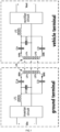
- the technical solutions adopted in the present invention is to provide a wireless charging system comprising: a pile terminal used for wireless charging; a ground terminal, including an inverter circuit connected with the pile terminal, a first LCC (inductor capacitor capacitor) compensation circuit connected with the inverter circuit, and a transmitter coil used for wireless charging; and a vehicle terminal, including a rectifier circuit connected with an on-board battery, a second LCC compensation circuit connected with the rectifier circuit, and a receiver coil matching with the transmitter coil, wherein the transmitter coil and the receiver coil are all provided with a tap structure.
- the transmitter coil includes a first coil and a second coil that are used to form the center tap structure; a second end of the first coil is connected with a first end of the second coil to form a center tapped end; the receiver coil includes a third coil and a fourth coil that are used to form the center tap structure; the third coil is configured to match the first coil, the fourth coil is configured to match the second coil, and a second end of the third coil is connected with a first end of the fourth coil to form a center tapped end.
- the first LCC compensation circuit includes an inductor LF1, a capacitor CF1, a capacitor C1A and a capacitor C1B; one end of the inductor LF1 is connected to the inverter circuit, the other end of the inductor LF1 is connected with the capacitor C1A in series, then connected to a first end of the first coil; one end of the capacitor C1B is connected between the inductor LF1 and the capacitor C1A, the other end the capacitor C1B is connected to a second end of the second coil; one end of the capacitor CF1 is connected between the inductor LF1 and the capacitor C1A, and the other end the capacitor CF1 is connected to the center tapped end of the transmitter coil.
- the second LCC compensation circuit includes an inductor LF2, a capacitor CF2, a capacitor C2A and a capacitor C2B, one end of the inductor LF2 is connected to the rectifier circuit, the other end of the inductor LF2 is connected with the capacitor C2A in series, then connected to a first end of the third coil, one end of the capacitor C2B is connected between the inductor LF2 and the capacitor C2A, the other end of the capacitor C2B is connected to a second end of the fourth coil; one end of the capacitor CF2 is connected between the inductor LF2 and the capacitor C2A, and the other end of the capacitor CF2 is connected to the center tapped end of the receiver coil.
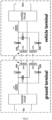
- the transmitter coil includes a first coil and a second coil arranged separately, and a second end of the first coil and a first end of the second coil together serve as a center tapped end of the transmitter coil;
- the receiver coil includes a third coil and a fourth coil arranged separately, the third coil is configured to match the first coil; the fourth coil is configured to match the third coil, and a second end of the third coil and a first end of the fourth coil together serve as a center tapped end of the receiver coil.
- the first LCC compensation circuit includes an inductor LF1, a capacitor CF1, a capacitor C1A and a capacitor C1B; one end of the inductor LF1 is connected to the inverter circuit, the other end of the inductor LF1 is connected with the capacitor C1A in series, then connected to a first end of the first coil; one end of the capacitor C1B is connected between the inductor LF1 and the capacitor C1A, the other end of the capacitor C1B is connected to a second end of the second coil; one end of the capacitor CF1 is connected between the inductor LF1 and the capacitor C1A, and the other end of the capacitor CF1 is connected to a second end of the first coil and a first end of the second coil, respectively.
- the second LCC compensation circuit includes an inductor LF2, a capacitor CF2, a capacitor C2A and a capacitor C2B; one end of the inductor LF2 is connected to the rectifier circuit, the other end of the inductor LF2 is connected with the capacitor C2A in series, then connected to a first end of the third coil, one end of the capacitor C2B is connected between the inductor LF2 and the capacitor C2A, the other end of the capacitor C2B is connected to a second end of the second coil; one end of the capacitor CF2 is connected between the inductor LF2 and the capacitor C2A, and the other end of the capacitor CF2 is connected to a second end of the third coil and a first end of the fourth coil, respectively.
- the inverter circuit includes a power switch transistor Q1, a power switch transistor Q2, a power switch transistor Q3, a power switch transistor Q4 that are used to form a full-bridge circuit, and the power switch transistor Q1 and the power switch transistor Q2 form a first bridge arm, and the power switch transistor Q3 and the power switch transistor Q4 form a second bridge arm;
- Drain electrodes of the power switch transistor Q1 and the power switch transistor Q3 are connected to a positive end of an input voltage Vin
- source electrodes of the power switch transistor Q2 and the power switch transistor Q4 are connected to a negative end of the input voltage Vin
- the inductor LF1 is connected between a source electrode of the power switch transistor Q1 and a drain electrode of the power switch transistor Q2
- the center tapped end of the transmitter coil is connected between a source electrode of the power switch transistor Q3 and a drain electrode of the power switch transistor Q4.
- duty ratios of the power switch transistor Q1, the power switch transistor Q2, the power switch transistor Q3 and the power switch transistor Q4 are set as 0.5, and the power switch transistor Q1 conducts with the power switch transistor Q2 in a complementary mode, and the power switch transistor Q3 conducts with the power switch transistor Q4 in a complementary mode; in addition, an output voltage of the inverter circuit is adjusted according to a phase shift angle between the power switch transistor Q2 and the power switch transistor Q4.
- the power switch transistor Q1 conducts with the power switch transistor Q2 in a complementary mode and the power switch transistor Q3 conducts with the power switch transistor Q4 in a complementary mode; in addition, a phase difference between the power switch transistor Q2 and the power switch transistor Q4 is set to be ⁇ , and both the transistors have a same duty ratio, and the output voltage of the inverter circuit is adjusted according to the duty ratio of the power switch transistor Q2 and the power switch transistor Q4.
- the rectifier circuit includes a power switch transistor Q5, a power switch transistor Q6, a power switch transistor Q7, a power switch transistor Q8 that are used to form a full-bridge circuit, and the power switch transistor Q5 and the power switch transistor Q6 form a third bridge arm, and the power switch transistor Q7 and the power switch transistor Q8 form a fourth bridge arm; drain electrodes of the power switch transistor Q5 and the power switch transistor Q7 are connected to a positive end of an output voltage Vout, source electrodes of the power switch transistor Q6 and the power switch transistor Q8 are connected to a negative end of the output voltage Vout, the inductor LF2 is connected between a source electrode of the power switch transistor Q5 and a drain electrode of the power switch transistor Q6, and the center tapped end of the receiver coil is connected between a source electrode of the power switch transistor Q7 and a drain electrode of the power switch transistor Q8.
- duty ratios of the power switch transistor Q5, the power switch transistor Q6, the power switch transistor Q7 and the power switch transistor Q8 are set as 0.5, and the power switch transistor Q5 conducts with the power switch transistor Q6 in a complementary mode, and the power switch transistor Q7 conducts with the power switch transistor Q8 in a complementary mode; in addition, an input voltage of the rectifier circuit is adjusted according to a phase shift angle between the power switch transistor Q6 and the power switch transistor Q8.
- the power switch transistor Q5 conducts with the power switch transistor Q6 in a complementary mode and the power switch transistor Q7 conducts with the power switch transistor Q8 in a complementary mode; in addition, a phase difference between the power switch transistor Q6 and the power switch transistor Q8 is set to be ⁇ , and both the transistors have a same duty ratio, and the input voltage of the rectifier circuit is adjusted according to the duty ratio of the power switch transistor Q6 and the power switch transistor Q8.
- the rectifier circuit includes a diode D5, a diode D7, a power switch transistor Q6, and a power switch transistor Q8;
- Negative electrodes of the diode D5 and the diode D7 are connected to a positive end of an output voltage Vout; source electrodes of the power switch transistor Q6 and the power switch transistor Q8 are connected to a negative end of the output voltage Vout, and the inductor LF2 is connected between a positive electrode of the diode D5 and a drain electrode of the power switch transistor Q6, and the center tapped end of the receiver coil is connected between a positive electrode of the diode D7 and a drain electrode of the power switch transistor Q8.
- a phase difference between the power switch transistor Q6 and the power switch transistor Q8 is set to be ⁇ ; in addition, the power switch transistor Q6 and the power switch transistor Q8 have a same duty ratio, and an input voltage of the rectifier circuit is adjusted according to the duty ratio of the power switch transistor Q6 and the power switch transistor Q8.
- C F 1 is a capacitance value of the capacitor CF1
- C 1 A is a capacitance value of the capacitor C1A
- C 1 B is a capacitance value of the capacitor C1B
- L F 1 is an inductance of the inductor LF1
- L BPA is an inductance of the first coil
- L BPB is an inductance of the second coil
- W 0 is a resonant angle frequency of the capacitor Cf1 and the inductor LF1
- L BPAllk is a leakage inductance of the first coil
- L BPBllk is a leakage inductance of the second coil
- L m is a mutual inductance of
- L VPA L VPAllk + L m ;
- L VPB L VPBllk + L m ;
- C F 2 is a capacitance value of the capacitor CF2
- C 2 A is a capacitance value of the capacitor C2A
- C 2 B is a capacitance value of the capacitor C2B
- L F 2 is an inductance of the inductor LF2
- L vPA is an inductance of the third coil
- L VPB is an inductance of the fourth coil
- W 0 is a resonant angle frequency of the capacitor Cf1 and the inductor LF1
- L VPAllk is a leakage inductance of the third coil
- L VPBllk is a leakage inductance of the fourth coil
- L m is a mutual
- the present invention further provides an electric vehicle having the wireless charging system as above.
- the present invention has at least the following beneficial effects.
- the transmitter coil and the receiver coil are provided with a tap structure, which can enable the voltages of the transmitter coil and the receiver coil to decrease by one time, solving the insulation and safety control problems caused by the high voltages of the transmitter coil and the receiver coil, improving the reliability of products and reducing development costs and material costs for products.
- the idea of the present invention is that the transmitter coil and the receiver coil are replaced with a tap structure, which can enable the voltages of the transmitter coil and the receiver coil to decrease by one time.
- the wireless charging system proposed by the present invention includes a pile terminal used for wireless charging, a ground terminal, and a vehicle terminal, wherein the pile terminal is used as an energy supply unit, which is generally floor-mounted or wall-mounted, and input with AC mains, rectifying an alternating current into a direct current, and generating high-frequency currents through an inverter;
- the ground terminal acting as a transmitter is installed on the ground or underground and connected with the pile terminal through a cable, converting the high-frequency currents generated by the pile terminal into magnetic field energy and transmitting it;
- the vehicle terminal acting as a receiver is installed on the bottom of a vehicle, receiving the magnetic field energy, and charging an electric vehicle battery through rectified induced currents result from the magnetic field energy.
- the pile terminal, the ground terminal, and the vehicle terminal cooperate with each other, so it is achievable to realize wirelessly electric vehicles charging and avoid the electric arcs and electric sparks caused by high-power charging.
- the ground terminal includes an inverter circuit connected with the pile terminal, a first LCC compensation circuit connected with the inverter circuit, and a transmitter coil used for wireless charging.
- the vehicle terminal includes a rectifier circuit connected with an on-board battery, a second LCC compensation circuit connected with the rectifier circuit, and a receiver coil matching with the transmitter coil.
- the inverter circuit can convert the direct current transmitted by the pile terminal into the alternating current, which the first LCC compensation circuit compensates for, and transmits to the receiver coil through the transmitter coil; after the receiver coil receives the energy transmitted by the transmitter coil, the second LCC compensation circuit compensates for the alternating current, which is finally rectified by the rectifier circuit into direct current for charging the on-board battery, so as to realize the function of wirelessly charging on-board batteries.
- the transmitter coil and the receiver coil are all provided with a tap structure in the present invention.
- the transmitter coil includes a first coil and a second coil that are used to form a center tap structure, wherein a second end of the first coil is connected with a first end of the second coil to form a center tapped end;
- the receiver coil includes a third coil and a fourth coil that are used to form a center tap structure, wherein the third coil is configured to match the first coil, the fourth coil is configured to match the second coil, and a second end of the third coil is connected with a first end of the fourth coil to form a center tapped end.
- LBPA is the first coil
- LBPB is the second coil
- LVPA is the third coil
- LVPB is the fourth coil
- an inductor LF1, a capacitor CF1, a capacitor C1A and a capacitor C1B form a first LCC compensation circuit
- an inductor LF2, a capacitor CF2, a capacitor CA and a capacitor C2B form a second LCC compensation circuit
- Lm is defined as a mutual inductance of a loosely coupled transformer (a transformer composed of the transmitter coil and the receiver coil), and LBPAllk represents a leakage inductance of LBPA, LBPBllk represents a leakage inductance of LBPB, LVPAllk represents a leakage inductance of LVPA, and LVPBllk represents a leakage inductance of LVPB.
- L BPA L BPAllk + L m ;
- L BPB L BPBllk + L m ;
- L VPA L VPAllk + L m ;
- L VPB L VPBllk + L m ;
- VAB is a fundamental voltage obtained after passing an input voltage Vin through the inverter circuit, that is, an output voltage of the inverter circuit
- Vab is a fundamental voltage obtained before passing an output voltage Vout through the inverter circuit, that is, an input voltage of the inverter circuit
- WO represents a resonant angle frequency of the inductor LF1 and capacitor CF1 (WO also represents a resonant angle frequency of the inductor LF2 and capacitor CF2); it is possible to obtain the following formulas.
- C 1 A + L BPAllk C 1 B + L BPBllk ;
- C 2 A + L VPAllk C 2 B + L VPBllk ;
- I VPB V ab C 2 A + L VPAllk ⁇ C 2 B + L VPBllk C 2 A + L VPAllk + C 2 B + L VPBll
- the transmitter coil of the center tap structure composed of LBPA and LBPB is split into two transmitter coils that are independently connected in parallel with each other. It is convenient for this connection to form the two coils, further reducing costs.
- the transmitter coil includes a first coil and a second coil arranged separately, and the second end of the first coil and the first end of the second coil together serve as a center tapped end of the transmitter coil.
- the receiver coil includes a third coil and a fourth coil arranged separately, the third coil is configured to match the first coil; the fourth coil is configured to match the third coil, and the second end of the third coil and the first end of the fourth coil together serve as a center tapped end of the receiver coil.
- one end of the inductor LF1 is connected to the inverter circuit, the other end of the inductor LF1 is connected with the capacitor C1A in series, then connected to the first end of the first coil; one end of the capacitor C1B is connected between the inductor LF1 and the capacitor C1A, the other end of the capacitor C1B is connected to the second end of the second coil; one end of the capacitor CF1 is connected between the inductor LF1 and the capacitor C1A, and the other end of the capacitor CF1 is connected to the second end of the first coil and the first end of the second coil, respectively.
- one end of the inductor LF2 is connected to the rectifier circuit, the other end of the inductor LF2 is connected with the capacitor C2A in series, then connected to the first end of the third coil, one end of the capacitor C2B is connected between the inductor LF2 and the capacitor C2A, the other end of the capacitor C2B is connected to the second end of the second coil; one end of the capacitor CF2 is connected between the inductor LF2 and the capacitor C2A, and the other end of the capacitor CF2 is connected to the second end of the third coil and the first end of the fourth coil, respectively.
- IBPA and IBPB are equal to each other, IVPA and IVPB are equal to each other.
- the transmitter coil and the receiver coil should meet the following conditions.
- C 1 A + L BPAllk C 1 B + L BPBllk ;
- C 2 A + L VPAllk C 2 B + L VPBllk ;
- C 1 A is a capacitance value of the capacitor C1A
- C 1 B is a capacitance value of the capacitor C1B
- C 2 A is a capacitance value of the capacitor C2A
- C 2 B is a capacitance value of the capacitor C2B
- L BPAllk is a leakage inductance of the first coil
- L BPBllk is a leakage inductance of the second coil
- L VPAllk is a leakage inductance of the third coil
- L VPBllk is a leakage inductance of the fourth coil.
- the inverter circuit in the present invention includes a power switch transistor Q1, a power switch transistor Q2, a power switch transistor Q3, a power switch transistor Q4 that are used to form a full-bridge circuit, and the power switch transistor Q1 and the power switch transistor Q2 form a first bridge arm, and the power switch transistor Q3 and the power switch transistor Q4 form a second bridge arm.
- Drain electrodes of the power switch transistor Q1 and the power switch transistor Q3 are connected to a positive end of the input voltage Vin
- source electrodes of the power switch transistor Q2 and the power switch transistor Q4 are connected to a negative end of the input voltage Vin
- the inductor LF1 is connected between a source electrode of the power switch transistor Q1 and a drain electrode of the power switch transistor Q2
- the center tapped end of the transmitter coil is connected between a source electrode of the power switch transistor Q3 and a drain electrode of the power switch transistor Q4.
- the power switch transistor Q1 ⁇ the power switch transistor Q4 it is possible to use active devices such as MOS transistors and IGBT transistors.
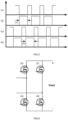
- Fig.4 is a control timing diagram of each power switch transistor in the inverter circuit.
- setting the duty ratios of the power switch transistor Q1, the power switch transistor Q2, the power switch transistor Q3 and the power switch transistor Q4 as 0.5, so that the power switch transistor Q1 conducts with the power switch transistor Q2 in a complementary mode, and the power switch transistor Q3 conducts with the power switch transistor Q4 in a complementary mode; in addition, the output voltage (fundamental voltage VAB) of the inverter circuit is adjusted according to a phase shift angle between the power switch transistor Q2 and the power switch transistor Q4.
- the output voltage (fundamental voltage VAB) of the inverter circuit is adjusted according to a phase shift angle between the power switch transistor Q2 and the power switch transistor Q4.
- the above inverter circuit can give the following calculation formulas according to the Fourier decomposition.
- V AB V in ⁇ 2 2 ⁇ ⁇ sin ⁇ ⁇ ⁇ 1 ;
- F 1 V in ⁇ 2 ⁇ ⁇ sin ⁇ ⁇ ⁇ 1 w 0 ⁇ L F 1 ;
- ⁇ 1 represents a phase shift angle between the power switch transistor Q2 and the power switch transistor Q4; it can be seen from the above formulas that by way of setting as above, the fundamental voltage VAB is only related to the input voltage Vin and the phase-shift angle ⁇ 1 , and the fundamental voltage VAB can be adjusted by means of the phase shift angle ⁇ 1 under the condition that the input voltage Vin is unchanged.
- the currents IBPA and IBPB in the first and second coils are only related to the input voltage Vin, the inductor LF1, and the phase shift angle ⁇ 1 , so when the input voltage Vin and the inductor LF1 remain unchanged, the currents IBPA and IBPB can be adjusted by means of the phase shift angle ⁇ 1 .
- the present invention is also configured with another control timing.
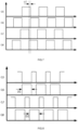
- the present invention is configured to enable the power switch transistor Q1 to conduct with the power switch transistor Q2 in a complementary mode and the power switch transistor Q3 to conduct with the power switch transistor Q4 in a complementary mode, as well as the phase difference between the power switch transistor Q2 and the power switch transistor Q4 to be ⁇ , so that both the transistors have the same duty ratio, and the fundamental voltage VAB is adjusted according to the duty ratio of the power switch transistor Q2 and the power switch transistor Q4.
- the above inverter circuit can give the following calculation formulas according to the Fourier decomposition.
- V AB V in ⁇ 2 2 ⁇ ⁇ sin ⁇ ⁇ 1 ⁇ D 1 ;
- F 1 V in ⁇ 2 ⁇ ⁇ sin ⁇ ⁇ 1 ⁇ D 1 w 0 ⁇ L F 1 ;
- D1 represents a duty ratio of the power switch transistor Q2 and the power switch transistor Q4; it can be seen from the above formulas that by way of setting as above, the fundamental voltage VAB is only related to the input voltage Vin and the duty ratio D1, and the fundamental voltage VAB can be adjusted by means of the duty ratio D1 under the condition that the input voltage Vin is unchanged.
- the currents IBPA and IBPB in the first and second coils are only related to the input voltage Vin, the inductor LF1, and the duty ratio D1, so when the input voltage Vin and the inductor LF1 remain unchanged, the currents IBPA and IBPB can be adjusted by means of the duty ratio D1.
- the currents of LVPA and LVPB can also be adjusted by changing the fundamental voltage Vab obtained before rectifying the output voltage Vout; the control timing of the present invention is described in combination with Fig.4 ;
- the rectifier circuit in the present invention includes a power switch transistor Q5, a power switch transistor Q6, a power switch transistor Q7, a power switch transistor Q8 that are used to form a full-bridge circuit, and the power switch transistor Q5 and the power switch transistor Q6 form a third bridge arm, and the power switch transistor Q7 and the power switch transistor Q8 form a fourth bridge arm.
- Drain electrodes of the power switch transistor Q5 and the power switch transistor Q7 are connected to a positive end of the output voltage Vout
- source electrodes of the power switch transistor Q6 and the power switch transistor Q8 are connected to a negative end of the output voltage Vout
- the inductor LF2 is connected between a source electrode of the power switch transistor Q5 and a drain electrode of the power switch transistor Q6, and the center tapped end of the receiver coil is connected between a source electrode of the power switch transistor Q7 and a drain electrode of the power switch transistor Q8.
- the power switch transistor Q5 ⁇ the power switch transistor Q8 it is possible to use active devices such as MOS transistors and IGBT transistors.
- Fig.7 is a control timing diagram of each power switch transistor in the rectifier circuit.
- the output voltage (fundamental voltage Vab) of the rectifier circuit is adjusted according to a phase shift angle between the power switch transistor Q6 and the power switch transistor Q8.
- the above rectifier circuit can give the following calculation formulas according to the Fourier decomposition.
- V ab V out ⁇ 2 2 ⁇ ⁇ sin ⁇ ⁇ ⁇ 2 ;
- ⁇ 2 represents a phase shift angle between the power switch transistor Q6 and the power switch transistor Q8; it can be seen from the above formulas that by way of setting as above, the fundamental voltage Vab is only related to the output voltage Vout and the phase-shift angle ⁇ 2 , and the fundamental voltage Vab can be adjusted by means of the phase shift angle ⁇ 2 under the condition that the output voltage Vout is unchanged.
- the currents IVPA and IVPB in the third and fourth coils are only related to the output voltage Vout, the inductor LF2, and the phase shift angle ⁇ 2 , so when the output voltage Vout and the inductor LF2 remain unchanged, the currents IVPA and IVPB can be adjusted by means of the phase shift angle ⁇ 2 .
- the present invention is also configured with another control timing.
- the present invention is configured to enable the power switch transistor Q5 to conduct with the power switch transistor Q6 in a complementary mode and the power switch transistor Q7 to conduct with the power switch transistor Q8 in a complementary mode, as well as the phase difference between the power switch transistor Q6 and the power switch transistor Q8 to be ⁇ , so that both the transistors have the same duty ratio, and the fundamental voltage Vab is adjusted according to the duty ratio of the power switch transistor Q6 and the power switch transistor Q8.
- the above rectifier circuit can give the following calculation formulas according to the Fourier decomposition.
- V ab V out ⁇ 2 2 ⁇ ⁇ sin ⁇ ⁇ 1 ⁇ D 2 ;
- D2 represents a duty ratio of the power switch transistor Q6 and the power switch transistor Q8; it can be seen from the above formulas that by way of setting as above, the fundamental voltage Vab is only related to the output voltage Vout and the duty ratio D2, and the fundamental voltage Vab can be adjusted by means of the duty ratio D2 under the condition that the output voltage Vout is unchanged.
- the currents IVPA and IVPB in the third and fourth coils are only related to the output voltage Vout, the inductor LF2, and the duty ratio D2, so when the output voltage Vout and the inductor LF2 remain unchanged, the currents IVPA and IVPB can be adjusted by means of the duty ratio D2.
- the rectifier circuit includes a diode D5, a diode D7, a power switch transistor Q6, and a power switch transistor Q8.
- Negative electrodes of the diode D5 and the diode D7 are connected to a positive end of the output voltage Vout; source electrodes of the power switch transistor Q6 and the power switch transistor Q8 are connected to a negative end of the output voltage Vout, and the inductor LF2 is connected between a positive electrode of the diode D5 and a drain electrode of the power switch transistor Q6, and the center tapped end of the receiver coil is connected between a positive electrode of the diode D7 and a drain electrode of the power switch transistor Q8.
- the present invention is also configured with another control timing.
- the present invention is configured to enable the phase difference between the power switch transistor Q6 and the power switch transistor Q8 to be ⁇ , so that both the transistors have the same duty ratio, and the input voltage (fundamental voltage Vab) of the rectifier circuit is adjusted according to the duty ratio of the power switch transistor Q6 and the power switch transistor Q8.
- the above rectifier circuit can give the following calculation formulas according to the Fourier decomposition.
- V ab V out ⁇ 2 2 ⁇ ⁇ sin ⁇ ⁇ 1 ⁇ D 3 ;
- D3 represents a duty ratio of the power switch transistor Q6 and the power switch transistor Q8; it can be seen from the above formulas that by way of setting as above, the fundamental voltage Vab is only related to the output voltage Vout and the duty ratio D3, and the fundamental voltage Vab can be adjusted by means of the duty ratio D3 under the condition that the output voltage Vout is unchanged.
- the currents IVPA and IVPB in the third and fourth coils are only related to the output voltage Vout, the inductor LF2, and the duty ratio D3, so when the output voltage Vout and the inductor LF2 remain unchanged, the currents IVPA and IVPB can be adjusted by means of the duty ratio D3.
- each device in the ground terminal of the present invention should meet the following conditions.
- C F 1 ⁇ L F 1 1 w 0 2 ;
- L BPA L BPAllk + L m ;
- L BPB L BPBllk + L m ;
- C F 1 is a capacitance value of the capacitor CF1
- C 1 A is a capacitance value of the capacitor C1A
- C 1 B is a capacitance value of the capacitor C1B
- L F 1 is an inductance of the inductor LF1
- L BPA is an inductance of the first coil
- L BPB is an inductance of the second coil
- WO is a resonant angle frequency of the capacitor CF1 and the inductor LF1
- L BPAllk is a leakage inductance of the first coil
- L BPBllk is a leakage inductance of the second coil
- L m is a mutual inductance of the transmitter coil and the receiver coil.
- each device in the vehicle terminal should meet the following conditions.
- C F 2 ⁇ L F 2 1 w 0 2 ;
- L VPA L VPAllk + L m ;
- L VPB L VPBllk + L m ;
- C F 2 is a capacitance value of the capacitor CF2
- C 2 A is a capacitance value of the capacitor C2A
- C 2 B is a capacitance value of the capacitor C2B
- L F 2 is an inductance of the inductor LF2
- L vPA is an inductance of the third coil
- L VPB is an inductance of the fourth coil
- WO is a resonant angle frequency of the capacitor CF1 and the inductor LF1 (the resonant angle frequency of the capacitor CF2 and the inductor LF2 is same as the resonant angle frequency of the capacitor CF1 and the inductor LF1, each of the two is WO)
- L VPAllk is a leakage inductance of the third coil
- L VPBllk is a leakage inductance of the fourth coil
- L m is a mutual inductance of the transmitter coil and the receiver coil.
- the invention also proposes an electric vehicle, which adopts the wireless charging system described above.
- the electric vehicle includes at least a low-speed four-wheeled electric vehicle, a low-speed two-wheeled electric vehicle, a low-speed logistics vehicle, a four-wheeled passenger vehicle, a four-wheeled commercial vehicle and the likes.
- the transmitter coil and the receiver coil are provided with a tap structure, which can enable the voltages of the transmitter coil and the receiver coil to decrease by one time, solving the insulation and safety control problems caused by the high voltages of the transmitter coil and the receiver coil, improving the reliability of products and reducing development costs and material costs for products.
Landscapes
- Engineering & Computer Science (AREA)
- Power Engineering (AREA)
- Computer Networks & Wireless Communication (AREA)
- Transportation (AREA)
- Mechanical Engineering (AREA)
- Physics & Mathematics (AREA)
- Electromagnetism (AREA)
- Charge And Discharge Circuits For Batteries Or The Like (AREA)
- Inverter Devices (AREA)
Applications Claiming Priority (2)
| Application Number | Priority Date | Filing Date | Title |
|---|---|---|---|
| CN202211477602.7A CN116317042A (zh) | 2022-11-23 | 2022-11-23 | 一种无线充电系统及电动汽车 |
| PCT/CN2023/096669 WO2024108949A1 (zh) | 2022-11-23 | 2023-05-26 | 一种无线充电系统及电动汽车 |
Publications (2)
| Publication Number | Publication Date |
|---|---|
| EP4451509A1 true EP4451509A1 (de) | 2024-10-23 |
| EP4451509A4 EP4451509A4 (de) | 2025-04-30 |
Family
ID=86822748
Family Applications (1)
| Application Number | Title | Priority Date | Filing Date |
|---|---|---|---|
| EP23893050.7A Pending EP4451509A4 (de) | 2022-11-23 | 2023-05-26 | Drahtloses ladesystem und elektrofahrzeug |
Country Status (4)
| Country | Link |
|---|---|
| US (1) | US20240399900A1 (de) |
| EP (1) | EP4451509A4 (de) |
| CN (1) | CN116317042A (de) |
| WO (1) | WO2024108949A1 (de) |
Families Citing this family (1)
| Publication number | Priority date | Publication date | Assignee | Title |
|---|---|---|---|---|
| CN116317042A (zh) * | 2022-11-23 | 2023-06-23 | 深圳威迈斯新能源股份有限公司 | 一种无线充电系统及电动汽车 |
Family Cites Families (10)
| Publication number | Priority date | Publication date | Assignee | Title |
|---|---|---|---|---|
| DE102013004179A1 (de) * | 2013-03-12 | 2014-09-18 | Paul Vahle Gmbh & Co. Kg | Erhöhung der Phasenlagentoleranz von magnetischen Kreisen bei der berührungslosen Energieübertragung |
| US10144301B2 (en) * | 2016-02-18 | 2018-12-04 | Denso International America, Inc. | Optimized compensation coils for wireless power transfer system |
| CN107346918A (zh) * | 2016-05-06 | 2017-11-14 | 宁波微鹅电子科技有限公司 | 一种无线电能传输装置 |
| CN206364564U (zh) * | 2016-11-22 | 2017-07-28 | 中兴新能源汽车有限责任公司 | 无线充电副边装置及电动汽车 |
| US10680466B2 (en) * | 2017-03-17 | 2020-06-09 | Integrated Device Technology, Inc. | Circuits and systems for wireless power transmission |
| CN109617250B (zh) * | 2018-12-25 | 2022-03-15 | 东南大学 | 一种基于组合型拓扑的抗偏移无线电能传输系统 |
| CN211790895U (zh) * | 2020-02-17 | 2020-10-27 | 宁波道充科技有限公司 | 轻量化的无线充电接收端及无线充电系统 |
| CN111987811B (zh) * | 2020-07-28 | 2024-02-13 | 东北林业大学 | 一种基于正交叠层式磁耦合机构的三传能通道型无线充电系统 |
| CN115056660B (zh) * | 2022-06-22 | 2025-08-19 | 深圳威迈斯新能源(集团)股份有限公司 | 无线充电系统及其控制方法 |
| CN116317042A (zh) * | 2022-11-23 | 2023-06-23 | 深圳威迈斯新能源股份有限公司 | 一种无线充电系统及电动汽车 |
-
2022
- 2022-11-23 CN CN202211477602.7A patent/CN116317042A/zh active Pending
-
2023
- 2023-05-26 EP EP23893050.7A patent/EP4451509A4/de active Pending
- 2023-05-26 WO PCT/CN2023/096669 patent/WO2024108949A1/zh not_active Ceased
-
2024
- 2024-08-08 US US18/797,830 patent/US20240399900A1/en active Pending
Also Published As
| Publication number | Publication date |
|---|---|
| US20240399900A1 (en) | 2024-12-05 |
| CN116317042A (zh) | 2023-06-23 |
| WO2024108949A1 (zh) | 2024-05-30 |
| EP4451509A4 (de) | 2025-04-30 |
Similar Documents
| Publication | Publication Date | Title |
|---|---|---|
| US11770025B2 (en) | Wireless power transmission appratus and control method thereof | |
| WO2018126617A1 (zh) | 一种恒流恒压复合拓扑的无线充电电路 | |
| Lovison et al. | Secondary-side-only simultaneous power and efficiency control for two converters in wireless power transfer system | |
| US20240399900A1 (en) | Wireless charging system and electric vehicle | |
| US10811868B2 (en) | Electrical system and method for protecting a DC/DC converter | |
| CN116317618A (zh) | 光伏逆变器及其控制方法 | |
| Joseph et al. | Design and simulation of wireless power transfer for electric vehicle | |
| Singh et al. | Performance analysis of 3-phase active front end PWM rectifier for air-core two-coil WPT system configuration | |
| Shakya et al. | Implementation of Inductive Wireless Power Transmission system for Battery Charging applications | |
| CN106208268A (zh) | 基于变初级参数的恒流恒压感应式无线充电系统 | |
| Bukya et al. | Analysis of interoperability different compensation network in wireless EV charging systems | |
| Esfahani et al. | Modeling and tuning of parameters of a bidirectional wireless power transfer for interfacing evs with the dc smart grids | |
| CN111579920A (zh) | 故障检测装置和方法 | |
| CN216699623U (zh) | 一种无线充电系统电路 | |
| CN108110871B (zh) | 无线充电副边装置及电动汽车 | |
| CN206364564U (zh) | 无线充电副边装置及电动汽车 | |
| WO2024164459A1 (zh) | 一种无线充电系统及其控制方法 | |
| CN212627329U (zh) | 一种无线充电系统的发射端、接收端及无线充电系统 | |
| Li et al. | Design of inductively coupled power transfer systems with series-parallel compensation frameworks | |
| Liu et al. | A New Bi-directional Wireless EV Charging Controller Tolerant to Large Pad Misalignments | |
| Fang et al. | Analysis and Design of Three-Coil Wireless Power Transfer System with Split Transmitting Coils | |
| Bodian et al. | Double outputs resonant-based wireless charger for electric vehicle and robotic applications | |
| Ranjan et al. | Design and Development of a 3.2 kW Wireless Battery Charger for an Electric Vehicle with a High-Frequency Full-Bridge Converter Using MATLAB Simulink | |
| Bukya et al. | Design and performance analysis of compensation capacitors in PS topology for wireless system on receiver side | |
| Lai et al. | A Novel Wireless Power Transfer System with Reflex-Charging and Cell-Balancing Functions |
Legal Events
| Date | Code | Title | Description |
|---|---|---|---|
| STAA | Information on the status of an ep patent application or granted ep patent |
Free format text: STATUS: THE INTERNATIONAL PUBLICATION HAS BEEN MADE |
|
| PUAI | Public reference made under article 153(3) epc to a published international application that has entered the european phase |
Free format text: ORIGINAL CODE: 0009012 |
|
| STAA | Information on the status of an ep patent application or granted ep patent |
Free format text: STATUS: REQUEST FOR EXAMINATION WAS MADE |
|
| 17P | Request for examination filed |
Effective date: 20240716 |
|
| AK | Designated contracting states |
Kind code of ref document: A1 Designated state(s): AL AT BE BG CH CY CZ DE DK EE ES FI FR GB GR HR HU IE IS IT LI LT LU LV MC ME MK MT NL NO PL PT RO RS SE SI SK SM TR |
|
| A4 | Supplementary search report drawn up and despatched |
Effective date: 20250402 |
|
| RIC1 | Information provided on ipc code assigned before grant |
Ipc: B60L 53/12 20190101ALI20250327BHEP Ipc: H02J 50/70 20160101ALI20250327BHEP Ipc: H02J 50/40 20160101ALI20250327BHEP Ipc: H02J 50/12 20160101ALI20250327BHEP Ipc: B60L 53/122 20190101ALI20250327BHEP Ipc: H02J 7/06 20060101AFI20250327BHEP |
|
| DAV | Request for validation of the european patent (deleted) | ||
| DAX | Request for extension of the european patent (deleted) | ||
| GRAP | Despatch of communication of intention to grant a patent |
Free format text: ORIGINAL CODE: EPIDOSNIGR1 |
|
| STAA | Information on the status of an ep patent application or granted ep patent |
Free format text: STATUS: GRANT OF PATENT IS INTENDED |