EP4447035A1 - Goa circuit and display panel - Google Patents
Goa circuit and display panel Download PDFInfo
- Publication number
- EP4447035A1 EP4447035A1 EP21827378.7A EP21827378A EP4447035A1 EP 4447035 A1 EP4447035 A1 EP 4447035A1 EP 21827378 A EP21827378 A EP 21827378A EP 4447035 A1 EP4447035 A1 EP 4447035A1
- Authority
- EP
- European Patent Office
- Prior art keywords
- transistor
- scan signal
- pull
- signal
- chamfering
- Prior art date
- Legal status (The legal status is an assumption and is not a legal conclusion. Google has not performed a legal analysis and makes no representation as to the accuracy of the status listed.)
- Pending
Links
Images

Classifications
-
- G—PHYSICS
- G09—EDUCATION; CRYPTOGRAPHY; DISPLAY; ADVERTISING; SEALS
- G09G—ARRANGEMENTS OR CIRCUITS FOR CONTROL OF INDICATING DEVICES USING STATIC MEANS TO PRESENT VARIABLE INFORMATION
- G09G3/00—Control arrangements or circuits, of interest only in connection with visual indicators other than cathode-ray tubes
- G09G3/20—Control arrangements or circuits, of interest only in connection with visual indicators other than cathode-ray tubes for presentation of an assembly of a number of characters, e.g. a page, by composing the assembly by combination of individual elements arranged in a matrix no fixed position being assigned to or needed to be assigned to the individual characters or partial characters
-
- G—PHYSICS
- G09—EDUCATION; CRYPTOGRAPHY; DISPLAY; ADVERTISING; SEALS
- G09G—ARRANGEMENTS OR CIRCUITS FOR CONTROL OF INDICATING DEVICES USING STATIC MEANS TO PRESENT VARIABLE INFORMATION
- G09G3/00—Control arrangements or circuits, of interest only in connection with visual indicators other than cathode-ray tubes
- G09G3/20—Control arrangements or circuits, of interest only in connection with visual indicators other than cathode-ray tubes for presentation of an assembly of a number of characters, e.g. a page, by composing the assembly by combination of individual elements arranged in a matrix no fixed position being assigned to or needed to be assigned to the individual characters or partial characters
- G09G3/22—Control arrangements or circuits, of interest only in connection with visual indicators other than cathode-ray tubes for presentation of an assembly of a number of characters, e.g. a page, by composing the assembly by combination of individual elements arranged in a matrix no fixed position being assigned to or needed to be assigned to the individual characters or partial characters using controlled light sources
- G09G3/30—Control arrangements or circuits, of interest only in connection with visual indicators other than cathode-ray tubes for presentation of an assembly of a number of characters, e.g. a page, by composing the assembly by combination of individual elements arranged in a matrix no fixed position being assigned to or needed to be assigned to the individual characters or partial characters using controlled light sources using electroluminescent panels
- G09G3/32—Control arrangements or circuits, of interest only in connection with visual indicators other than cathode-ray tubes for presentation of an assembly of a number of characters, e.g. a page, by composing the assembly by combination of individual elements arranged in a matrix no fixed position being assigned to or needed to be assigned to the individual characters or partial characters using controlled light sources using electroluminescent panels semiconductive, e.g. using light-emitting diodes [LED]
- G09G3/3208—Control arrangements or circuits, of interest only in connection with visual indicators other than cathode-ray tubes for presentation of an assembly of a number of characters, e.g. a page, by composing the assembly by combination of individual elements arranged in a matrix no fixed position being assigned to or needed to be assigned to the individual characters or partial characters using controlled light sources using electroluminescent panels semiconductive, e.g. using light-emitting diodes [LED] organic, e.g. using organic light-emitting diodes [OLED]
- G09G3/3266—Details of drivers for scan electrodes
-
- G—PHYSICS
- G09—EDUCATION; CRYPTOGRAPHY; DISPLAY; ADVERTISING; SEALS
- G09G—ARRANGEMENTS OR CIRCUITS FOR CONTROL OF INDICATING DEVICES USING STATIC MEANS TO PRESENT VARIABLE INFORMATION
- G09G3/00—Control arrangements or circuits, of interest only in connection with visual indicators other than cathode-ray tubes
- G09G3/20—Control arrangements or circuits, of interest only in connection with visual indicators other than cathode-ray tubes for presentation of an assembly of a number of characters, e.g. a page, by composing the assembly by combination of individual elements arranged in a matrix no fixed position being assigned to or needed to be assigned to the individual characters or partial characters
- G09G3/34—Control arrangements or circuits, of interest only in connection with visual indicators other than cathode-ray tubes for presentation of an assembly of a number of characters, e.g. a page, by composing the assembly by combination of individual elements arranged in a matrix no fixed position being assigned to or needed to be assigned to the individual characters or partial characters by control of light from an independent source
- G09G3/36—Control arrangements or circuits, of interest only in connection with visual indicators other than cathode-ray tubes for presentation of an assembly of a number of characters, e.g. a page, by composing the assembly by combination of individual elements arranged in a matrix no fixed position being assigned to or needed to be assigned to the individual characters or partial characters by control of light from an independent source using liquid crystals
- G09G3/3611—Control of matrices with row and column drivers
- G09G3/3674—Details of drivers for scan electrodes
- G09G3/3677—Details of drivers for scan electrodes suitable for active matrices only
-
- G—PHYSICS
- G11—INFORMATION STORAGE
- G11C—STATIC STORES
- G11C19/00—Digital stores in which the information is moved stepwise, e.g. shift registers
- G11C19/28—Digital stores in which the information is moved stepwise, e.g. shift registers using semiconductor elements
-
- G—PHYSICS
- G09—EDUCATION; CRYPTOGRAPHY; DISPLAY; ADVERTISING; SEALS
- G09G—ARRANGEMENTS OR CIRCUITS FOR CONTROL OF INDICATING DEVICES USING STATIC MEANS TO PRESENT VARIABLE INFORMATION
- G09G2300/00—Aspects of the constitution of display devices
- G09G2300/04—Structural and physical details of display devices
- G09G2300/0404—Matrix technologies
- G09G2300/0408—Integration of the drivers onto the display substrate
-
- G—PHYSICS
- G09—EDUCATION; CRYPTOGRAPHY; DISPLAY; ADVERTISING; SEALS
- G09G—ARRANGEMENTS OR CIRCUITS FOR CONTROL OF INDICATING DEVICES USING STATIC MEANS TO PRESENT VARIABLE INFORMATION
- G09G2310/00—Command of the display device
- G09G2310/02—Addressing, scanning or driving the display screen or processing steps related thereto
- G09G2310/0264—Details of driving circuits
- G09G2310/0267—Details of drivers for scan electrodes, other than drivers for liquid crystal, plasma or OLED displays
-
- G—PHYSICS
- G09—EDUCATION; CRYPTOGRAPHY; DISPLAY; ADVERTISING; SEALS
- G09G—ARRANGEMENTS OR CIRCUITS FOR CONTROL OF INDICATING DEVICES USING STATIC MEANS TO PRESENT VARIABLE INFORMATION
- G09G2310/00—Command of the display device
- G09G2310/02—Addressing, scanning or driving the display screen or processing steps related thereto
- G09G2310/0264—Details of driving circuits
- G09G2310/0286—Details of a shift registers arranged for use in a driving circuit
-
- G—PHYSICS
- G09—EDUCATION; CRYPTOGRAPHY; DISPLAY; ADVERTISING; SEALS
- G09G—ARRANGEMENTS OR CIRCUITS FOR CONTROL OF INDICATING DEVICES USING STATIC MEANS TO PRESENT VARIABLE INFORMATION
- G09G2310/00—Command of the display device
- G09G2310/06—Details of flat display driving waveforms
- G09G2310/066—Waveforms comprising a gently increasing or decreasing portion, e.g. ramp
-
- G—PHYSICS
- G09—EDUCATION; CRYPTOGRAPHY; DISPLAY; ADVERTISING; SEALS
- G09G—ARRANGEMENTS OR CIRCUITS FOR CONTROL OF INDICATING DEVICES USING STATIC MEANS TO PRESENT VARIABLE INFORMATION
- G09G2310/00—Command of the display device
- G09G2310/08—Details of timing specific for flat panels, other than clock recovery
-
- G—PHYSICS
- G09—EDUCATION; CRYPTOGRAPHY; DISPLAY; ADVERTISING; SEALS
- G09G—ARRANGEMENTS OR CIRCUITS FOR CONTROL OF INDICATING DEVICES USING STATIC MEANS TO PRESENT VARIABLE INFORMATION
- G09G2320/00—Control of display operating conditions
- G09G2320/02—Improving the quality of display appearance
- G09G2320/0223—Compensation for problems related to R-C delay and attenuation in electrodes of matrix panels, e.g. in gate electrodes or on-substrate video signal electrodes
Definitions
- the present disclosure relates to a field of display technology, in particular to a GOA circuit and a display panel.
- Gate driver on array (GOA) technology means a gate driving circuit is integrated into an array substrate of a display panel to realize a driving mode of progressive scanning, so that a gate driving circuit portion can be omitted, a manufacturing cost can be reduced, and a panel narrow frame design can be realized, which is used for a variety of displays.
- RC delay resistance-capacitance delay
- the present disclosure provides a GOA circuit and a display panel to solve a technical problem that a scan signal waveform at different positions of the display panel varies greatly due to RC delay, and further affects a display effect of the display panel.
- the present disclosure provides a gate driver on array (GOA) circuit, comprising multi-stage cascade GOA units, wherein an N-th stage GOA unit comprises a pull-up control module, a pull-up module, a chamfering control module, and a pull-down module;
- GOA gate driver on array
- the chamfering control module is added in the N-th stage GOA unit to carry out chamfering processing on the N-th stage scan signal, so that the output N-th stage scan signal is a chamfering wave, so as to reduce loss degree of the N-th stage scan signal G(n).
- the pull-up control module comprises a first transistor, a gate of the first transistor and one of a source and a drain of the first transistor are connected to the (N-m)-th stage scan signal, and another one of the source and the drain of the first transistor is electrically connected to the first node.
- a circuit structure of the pull-up control module is simple and easy to simplify the process.
- a potential of the first node can be controlled by controlling the on and off of the first transistor through the (N-m)-th stage scan signal, and a timing is simple.
- the pull-up module comprises a second transistor, a gate of the second transistor is electrically connected to the first node, one of a source and a drain of the second transistor is connected to the clock signal, and another one of the source and the drain of the second transistor is electrically connected to the N-th stage scan signal output terminal.
- a circuit structure of the pull-up module is simple and easy to simplify the process.
- the N-th stage scan signal can be outputted by controlling the on and off of the second transistor and the potential of the clock signal, and a timing is simple.
- the chamfering control module comprises a third transistor, a gate of the third transistor is connected to the chamfering control signal, one of a source and a drain of the third transistor is connected to the first reference low level signal, and another one of the source and the drain of the third transistor is electrically connected to the N-th stage scan signal output terminal.
- a circuit structure of the pull-up module is simple and easy to simplify the process.
- the chamfering processing of the N-th stage scan signal can be realized, and a timing is simple.
- the N-th stage scan signal has a chamfering width adjusted according to a duty ratio of the chamfering control signal and a chamfering depth adjusted according to a channel length-to-width ratio of the third transistor.
- the channel length-to-width ratio of the third transistor can be designed according to the chamfering depth required by the N-th stage scan signal, and the process preparation can be carried out.
- each scan signal output by the GOA circuit has a corresponding chamfering depth, and it is not necessary to control the chamfering depth through subsequent signals.
- the first reference low level signal and the second reference low level signal are same signals.
- setting the first reference low level signal and the second reference low -level signal as same signals can reduce the wires in the GOA circuit and reduce the production cost.
- the pull-down module comprises a fourth transistor and a fifth transistor; both a gate of the fourth transistor and a gate of the fifth transistor are connected to the (N+m)-th stage scan signal, one of a source and a drain of the fourth transistor and one of a source and a drain of the fifth transistor are connected to the second reference low level signal, and another one of the source and the drain of the fourth transistor and another one of the source and the drain of the fifth transistor are electrically connected to the first node.
- the potential of the first node and the potential of the N-th stage scan signal can be pulled down simultaneously under control of the (N+m)-th stage scan signal and the second reference low level signal.
- the circuit structure and timing are simple, which is convenient to simplify the process.
- the N-th stage scan signal has a chamfering width adjusted according to a duty ratio of the chamfering control signal and a chamfering depth adjusted according to a voltage amplitude of the first reference low level signal.
- the N-th stage scan signal is modulated by adjusting the duty ratio of the chamfering control signal and the voltage amplitude of the first reference low level signal, and the adjustment mode is more flexible. According to practical application, the N-th stage scan signal with the required chamfering waveform can be obtained, and the application range is wider.
- a duty ratio of the chamfering control signal is less than a duty ratio of the N-th stage scan signal.
- the duty ratio of the chamfering control signal is less than that of the N-th stage scan signal, and only the high potential close to the falling edge of the N-th stage scan signal is chamfered. While reducing the signal difference, the high potential of the N-th stage scan signal can be retained to prevent affecting the charging efficiency of the display panel.
- the potential of the N-th stage scan signal is pulled down by the chamfering control module to a potential less than or equal to the second reference low level.
- the present disclosure further provides a display panel, comprising a display area and a gate driver on array (GOA) circuit integrally disposed on an edge of the display area, wherein the GOA circuit may be any GOA circuit above.
- GOA gate driver on array
- the present disclosure provides a GOA circuit and a display panel.
- the GOA circuit comprises multi-stage cascaded GOA units.
- the N-th stage GOA unit comprises the pull-up control module, the pull-up module, the chamfering control module, and the pull-down module.
- the chamfering control module is connected to the chamfering control signal and the first reference low level signal, and is electrically connected to the N-th stage scan signal output terminal to pull down the potential of the N-th stage scan signal before the pull-down module pulling down the potential of the first node and the potential of the N-th stage scan signal, under control of the chamfering control signal and the first reference low level signal.
- the chamfering control module is added in the N-th stage GOA unit to carry out chamfering processing on the N-th stage scan signal, so that the output N-th stage scan signal is a chamfering wave, so as to reduce loss degree of the N-th stage scan signal G(n), improve the display effect of the display panel, and reduce the production cost.
- first”, “second” are for illustrative purposes only and are not to be construed as indicating or imposing a relative importance or implicitly indicating the number of technical features indicated.
- a feature that limited by “first”, “second” may expressly or implicitly include at least one of the features, and therefore cannot be understood as a limitation on the present disclosure.
- the present disclosure provides a GOA circuit and a display panel, which will be described in detail below. It should be noted that an order of description of the following embodiments is not a limitation on a preferred order of the embodiments of the present disclosure.
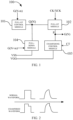
- FIG. 1 is a schematic structural diagram of an N-th stage GOA unit according to the present disclosure.
- a GOA circuit is provided in the present disclosure.
- the GOA circuit comprises multi-stage cascaded GOA units.
- the N-th stage GOA unit 100 comprises a pull-up control module 101, a pull-up module 102, a chamfering control module 103, and a pull-down module 104.
- the pull-up control module 101 is connected to an (N-m)-th stage scan signal G(N-m), and electrically connected to a first node Q(N).
- the pull-up control module 101 is configured to output the (N-m)-th stage scan signal G(N-m) to the first node Q(N) under the control of the (N-m)-th stage scan signal G(N-m).
- the pull-up module 102 receives a clock signal and is electrically connected to the first node Q(N) and an N-th stage scan signal output terminal.
- the pull-up module 102 is configured to output an N-th stage scan signal G(N) under the control of a potential of the first node Q(N) and the clock signal.
- the clock signal may be a current stage clock signal CK or a complementary clock signal XCK.
- the current stage clock signal CK and the complementary clock signal XCK remain inverted.
- a potential of the clock signal CK(N) of the current stage is high, a potential of the complementary clock signal XCK is low.
- the potential of the clock signal CKN of the current stage is low, the potential of the complementary clock signal XCK is high.
- the N-th stage GOA unit accesses the clock signal CK of the current stage.
- N-th stage GOA unit accesses the complementary clock signal XCK.
- the GOA circuit may also use only one clock signal.
- the chamfering control module 103 is connected to a chamfering control signal CT and a first reference low level signal VGG, and is electrically connected to the N-th scan signal output terminal P.
- the chamfering control module 103 is configured to pull down the potential of the N-th stage scan signal G(N) under control of the chamfering control signal CT and the first reference low level signal VGG.
- the pull-down module 104 is connected to an (N+m)-th scan signal G(N+m) and a second reference low level signal VSS, and is electrically connected to the first node Q(N) and the N-th level scan signal output terminal P.
- the pull-down module 104 is configured to pull down the potential of the first node Q(N) and the potential of the N-th level scan signal G(N) after the chamfering control module 103 pulls down the potential of the N-th level scan signal G(N) under the control of the (N+m)-th level scan signal G and the second reference low level VSS.
- N and m are both integers greater than zero.
- the value of N may be determined according to a driving architecture of the display panel and the number of scan lines.
- the value of m can be determined from the cascade relationship between the GOA units in the GOA circuit.
- m may be 1,3,4 or the like.
- a start signal may be provided in place of the scan signal G(N-m) to drive the pull-up control module 101 to operate.
- the chamfering control module 103 is added to the N-th stage GOA unit 100, and the N-th stage scan signal G(N) is pulled down before the pull-down module 104 pulls down the potential of the first node Q(N), thereby performing the chamfering processing on the N-th stage scan signal G(N) so that the output N-th stage scan signal G(N) is a chamfering wave.
- the chamfering control module 103 provided in the present disclosure greatly reduces the production cost of the display panel and improves the production efficiency.
- the potential of the N-th level scan signal G(N) is pulled down by the chamfering control module 103 to a potential less than or equal to the second reference low level VSS.
- the chamfering control module 103 typically pulls down the N-th stage scan signal G(N) to a potential greater than the second reference low level signal VSS. Then, the pull-down module 104 continues to pull it down to the potential of the second reference low level signal VSS.
- the chamfering control module 103 may also pull down the N-th stage scan signal G(N) directly to the potential of the second reference low level signal VSS. Then, the pull-down module 104 may maintain the potential of the N-th stage scan signal G(N) at the potential of the second reference low level signal VSS.
- the details may be determined according to the chamfering process of the chamfering control module 103. The following embodiment will be described in detail, and details are not described herein.
- FIG. 2 is a schematic diagram of transmission loss of an N-th stage scan signal of different waveforms according to the present disclosure.
- the N-th stage scan signal G(N) outputted from the N-th stage GOA unit 100 needs to be transmitted from an edge position to a center position of the display panel.
- the N-th stage scan signal G(N) is a normal waveform
- the waveform of the N-th stage scan signal G(N) changes due to signal loss due to RC delay during transmission, affecting charging efficiency.
- the N-th stage scan signal G(N) is a chamfering waveform
- the N-th stage scan signal G(N) after chamfering is also a chamfering waveform after transmission loss. Therefore, the waveform difference between the N-th stage scan signal G(N) before the loss and the N-th stage scan signal G(N) after the loss is small, thereby reducing the difference between the N-th stage scan signal G(N) at different positions of the display panel.
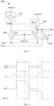
- FIG. 3 is a schematic circuit diagram of an N-th stage GOA unit according to the present disclosure.
- the pull-up control module 101 comprises a first transistor T1. Both a gate of the first transistor T1 and one of a source and a drain of the first transistor T1 are connected to the (N-m)-th stage scan signal G(N-m) Another one of the source and drain of the first transistor T1 is electrically connected to the first node Q(N).
- the pull-up control module 101 may also include a plurality of transistors in series, or a plurality of transistors operating alternately.
- the pull-up module 102 includes a second transistor T2.
- a gate of the second transistor T2 is electrically connected to the first node Q (N).
- One of a source and a drain of the second transistor T2 is connected to a clock signal, such as a current stage clock signal CK1 or a complementary clock signal CK2.
- Another one of the source and drain of the second transistor T2 is electrically connected to the N-th stage scan signal output terminal P.
- the pull-up module 102 may also include a plurality of transistors in series.
- the chamfering control module 103 comprises a third transistor T3.
- a gate of the third transistor T3 is connected to a chamfering control signal CT.
- One of a source and a drain of the third transistor T3 is connected to the first reference low level signal VGG.
- Another one of the source and the drain of the third transistor T3 is electrically connected to the N-th stage scan signal output terminal P.
- the pull-down module 104 comprises a fourth transistor T4 and a fifth transistor T5.
- a gate of the fourth transistor T4 and a gate of the fifth transistor T5 are both connected to the (N+m)-th stage scan signal G(N+m).
- One of a source and a drain of the fourth transistor T4 and one of a source and a drain of the fifth transistor T5 are connected to the second reference low level signal VSS.
- Another one of the source and drain of the fourth transistor T4 and another one of the source and drain of the fifth transistor T5 are electrically connected to the first node Q(N).
- the transistors used in the present disclosure may include two types of P-type transistors and/or N-type transistors.
- the P-type transistor is turned on when a gate is at a low level and turned off when the gate is at a high level.
- the N-type transistor is turned on when a gate is at a high level and turned off when the gate is at a low level.
- the transistors used in the present disclosure may be thin film transistors or field effect transistors or other devices having same characteristics. Since the sources and drains of the transistors used herein are symmetrical, the sources and drains thereof are interchangeable. In the present disclosure, to distinguish between two poles of a transistor other than a gate, one of the poles is referred to as a source and the other as a drain.
- an intermediate terminal of a switching transistor is a gate
- a signal input terminal is a source
- an output terminal is a drain.
- FIG. 4 is a schematic circuit diagram of an N-th stage GOA unit according to the present disclosure.
- the N-th stage GOA unit 100 comprises the following operating processes:
- the first transistor T1 is turned on when the (N-m)-th stage scan signal G(N-m) is raised to a high potential.
- the potential of the first node Q(N) is pulled up to the potential of the (N-m)-th stage scan signal G(N-m). Since the potential of the first node Q(N) is pulled high, the second transistor T2 is turned on.
- the clock signal CK of this stage rises from a low potential to a high potential, thereby outputting the N-th stage scan signal G(N) at the N-th stage scan signal output terminal P through the second transistor T2.
- the chamfering control signal CT rises from the low potential to the high potential.
- the third transistor T3 is turned on.
- the N-th stage scan signal output P is in communication with the first reference low level signal VGG. Accordingly, the N-th stage scan signal G(N) is pulled down, and the waveform of the N-th stage scan signal G(N) is changed so that the N-th stage scan signal G (N) becomes a chamfering wave.
- the (N+m)-th stage scan signal G(N+m) rises from the low potential to the high potential, and both the fifth transistor T5 and the fourth transistor T4 are turned on.
- Both the first node Q(N) and the N-th stage scan signal output terminal P are in communication with the second reference low level signal VSS. That is, the potential of the first node Q(N) and the potential of the N-th stage scan signal G(N) are both pulled down to the potential of the second reference low level VSS.
- an output of an (N+1)-th stage scan signal G(N+1) and the chamfering process are cyclically reciprocated to output the multi-stage scan signal as described above.
- the chamfering control module 103 is added to the N-th stage GOA unit 100, so that the N-th stage scan signal G(N) is first pulled down one step before the pull-down module 104 pulls down the N-th stage scan signal G(N), thereby realizing two-stage pull-down to achieve the purpose of the chamfering waveform of the output N-th stage scan signal G(N).
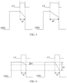
- FIG. 5 is a schematic diagram of a first chamfering theory of an N-th stage scan signal according to the present disclosure.
- FIG. 6 is a schematic diagram of a second chamfering theory of an N-th stage scan signal provided by the present disclosure.
- the N-th stage scan signal G(N) has a chamfering width and a chamfering depth.
- the chamfering width is adjusted according to a duty ratio of the chamfering control signal CT.
- the duty cycle refers to a ratio of a energizing time to a total time in a pulse cycle.
- the chamfering width of the N-th stage scan signal G(N) is a1.
- the duration of the high level of the chamfering control signal CT is a2
- the chamfering width of the N-th stage scan signal G(N) is a2. It can be seen that the larger the duty ratio of the chamfering control signal CT, the larger the chamfering width of the N-th scan signal G(N). Therefore, the chamfering width of the N-th stage scan signal G(N) can be adjusted by the duty ratio of the chamfering control signal CT.
- the chamfering depth of the N-th stage scan signal G(N) may be adjusted according to a voltage amplitude of the first reference low-level signal VGG or a channel length-width ratio of the third transistor T3.
- the chamfering process of the N-th stage scan signal G(N) is a pull-down process of the N-th stage scan signal G(N).
- a level height of the N-th stage scan signal G(N) is pulled down from an initial high level to an intermediate level or down to a low level during the time that the N-th stage scan signal G(N) is chamfered. Therefore, during the chamfering process, a level change amount of the N-th stage scan signal G(N) is the chamfering depth of the N-th stage scan signal G(N).
- the chamfering width of the N-th stage scan signal G(N) is the same.
- the greater the voltage amplitude of the first reference low level signal VGG the greater the chamfering depth of the N-th-stage scan signal G(N).
- the chamfering depth of the N-th stage scan signal G(N) is small, and is b 1.
- the pull-down speed of the N-th stage scan signal G(N) is fast, and the pull-down amplitude is large in the same pull-down time.
- the scan signal G(N) of the N-th stage has a larger chamfering depth, and is b2.
- the N-th stage scan signal G(N) may be chamfered in a plurality of ways.
- the waveform of the N-th stage scan signal G(N) may be modulated according to the chamfering control signal CT, the channel length-to-width ratio of the third transistor T3, and/or the voltage amplitude of the first reference low level signal VGG.
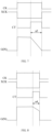
- FIG. 7 is a schematic diagram of generating a first waveform of an N-th stage scan signal according to the present disclosure.
- the duty ratio of the chamfering control signal CT is large, and the chamfering width of the N-th scan signal G(N) is a3.
- the channel length-to-width of the third transistor T3 are relatively large, and/or the voltage amplitude of the first reference low level signal VGG is large, and the pull-down speed is fast.
- the N-th stage scan signal G(N) is pulled down directly from the high level to the low level. This low level may be equal to the potential of the second reference low level signal VSS.
- FIG. 8 is a schematic diagram of generating a second waveform of an N-th stage scan signal according to the present disclosure.
- the duty ratio of the chamfering control signal CT is centered, and the chamfering width of the N-th scan signal G(N) is a4, a4 ⁇ a3.
- the channel length-to-width ratio of the third transistor T3 and/or the voltage amplitude of the first reference low level signal VGG are adjusted to a suitable range such that, during the pull-down process, the N-th stage scan signal G(N) is pulled down from the high level to an intermediate level and not down to the low level. This intermediate level is less than the potential of the second reference low level signal VSS.
- FIG. 9 is a schematic diagram of generating a third waveform of an N-th stage scan signal according to the present disclosure.
- the duty ratio of the chamfering control signal CT is less, and the chamfering width of the N-th stage scan signal GN is a5, a5 ⁇ a4 ⁇ a3.
- the channel length-to-width ratio of the third transistor T3 are relatively large, and/or the voltage amplitude of the first reference low level signal VGG is large, and the pull-down speed is extremely fast.
- the pull-down process is very short. Therefore, although the pull-down time is shorter than in FIG. 8 , the voltage amplitude of the N-th stage scan signal G(N) can also be pulled down by a certain amplitude, and is not pulled down to the potential of the second reference low level signal VSS.
- the waveforms of the N-th stage scan signal G (N) shown in FIGs. 7 to 9 are merely illustrative of the solution of the present disclosure and cannot be understood as a limitation of the present disclosure. According to actual demands, the N-th stage scan signal G(N) having the desired chamfering waveform can be obtained by adjusting the chamfering control signal CT, the channel length-to-width ratio of the third transistor T3, and/or the voltage amplitude of the first reference low level signal VGG.
- the first reference low level signal VGG and the second reference low level signal VSS are the same signal. This reduces wires in the GOA circuit and reduces production costs. At this time, the voltage amplitude of the first reference low level signal VGG is fixed. Therefore, it is possible to adjust the chamfering depth of the N-th stage scan signal G(N) only by adjusting the channel length-to-width ratio of the third transistor T3.
- the duty ratio of the chamfering control signal CT is less than the duty ratio of the N-th stage scan signal G(N). It will be understood that the waveform deterioration of the N-th stage scan signal G(N) is mainly reflected in a falling edge due to the transmission loss caused by RC delay.
- the duty ratio of the chamfering control signal CT is set to be less than the duty ratio of the N-th stage scan signal G(N), and only the high potential close to the falling edge of the N-th stage scan signal G(N) is chamfered, so that the high potential of the N-th stage scan signal G(N) can be retained while the signal difference is reduced, thereby preventing affecting the charging efficiency of the display panel.
- the N-th stage GOA unit 100 comprises only the pull-up control module 101, the pull-up module 102, the chamfering control module 103, and the pull-down module 104, but is not understood as a limitation of the present disclosure.
- the N-th stage GOA unit 100 may further comprise a reset module, a pull-down maintenance module, and the like, which are techniques well known to those skilled in the art and are not described herein again. That is, the chamfering control module 103 in the N-th stage GOA unit 100 provided herein may be applied to various types of GOA circuits.
- the present disclosure further provides a display panel.
- the display panel comprises GOA circuitry.
- the GOA circuit is configured to provide a scan signal required for the display screen of the display panel.
- the GOA circuit is the GOA circuit described in any one of the above embodiments. For details, refer to the above description.
- FIG. 10 is a schematic structural diagram of a display panel according to the present disclosure.
- the display panel 1000 comprises a display area AA and GOA circuits 200 integrally disposed on edges of the display area AA.
- the GOA circuits 200 comprise multi-stage cascaded GOA units.
- the GOA circuits 200 are provided on both sides of the display panel 1000.
- the N-th stage GOA unit comprises a pull-up control module, a pull-up module, a chamfering control module, and a pull-down module.
- the chamfering control module is added to the N-th stage GOA unit 100 to perform chamfering processing on the N-th stage scan signal, so that the output N-th stage scan signal is a chamfering wave, thereby reducing the loss degree of the N-th stage scan signal and improving the display effect of the display panel.
- the display panel 1000 provided in the present disclosure is described by way of example in which the GOA circuits 200 are provided on both sides of the display area AA in a double-sided driving manner. However, it cannot be understood as a limitation to the present disclosure. In some embodiments, a one-side driving or other driving mode may be used according to actual requirements of the display panel 1000, which is specifically limited herein.
Landscapes
- Engineering & Computer Science (AREA)
- Physics & Mathematics (AREA)
- Computer Hardware Design (AREA)
- General Physics & Mathematics (AREA)
- Theoretical Computer Science (AREA)
- Chemical & Material Sciences (AREA)
- Crystallography & Structural Chemistry (AREA)
- Control Of Indicators Other Than Cathode Ray Tubes (AREA)
- Liquid Crystal Display Device Control (AREA)
Abstract
Description
- The present disclosure relates to a field of display technology, in particular to a GOA circuit and a display panel.
- Gate driver on array (GOA) technology means a gate driving circuit is integrated into an array substrate of a display panel to realize a driving mode of progressive scanning, so that a gate driving circuit portion can be omitted, a manufacturing cost can be reduced, and a panel narrow frame design can be realized, which is used for a variety of displays.
- Due to the presence of resistance-capacitance delay (RC delay) in a display panel, a scan signal waveform at different positions of the display panel varies with transmission loss of the scan signal. The larger a size of the display panel, the more severe deterioration of the scan signal waveform, and problems such as flickering, poor uniformity of charging rate, and severe color deviation easily occur, thereby affecting a display effect of the display panel.
- The present disclosure provides a GOA circuit and a display panel to solve a technical problem that a scan signal waveform at different positions of the display panel varies greatly due to RC delay, and further affects a display effect of the display panel.
- The present disclosure provides a gate driver on array (GOA) circuit, comprising multi-stage cascade GOA units, wherein an N-th stage GOA unit comprises a pull-up control module, a pull-up module, a chamfering control module, and a pull-down module;
- the pull-up control module is connected to an (N-m)-th stage scan signal, and is electrically connected to a first node, and the pull-up control module is configured to output the (N-m)-th stage scan signal to the first node under control of the (N-m)-th stage scan signal, wherein N and m are integers greater than zero, and N>m;
- the pull-up module is connected to a clock signal and is electrically connected to the first node and an N-th stage scan signal output terminal, and the pull-up module is configured to output the N-th stage scan signal under control of a potential of the first node and the clock signal;
- the chamfering control module is connected to a chamfering control signal and a first reference low level signal, and is electrically connected to the N-th scan signal output terminal, and the chamfering control module is configured to pull down a potential of the N-th scan signal under control of the chamfering control signal and the first reference low level signal; and
- the pull-down module is connected to an (N+m)-th stage scan signal and a second reference low level signal, and is electrically connected to the first node and the N-th stage scan signal output terminal, and the pull-down module is configured to pull down the potential of the first node and the potential of the N-th stage scan signal after the chamfering control module pulls down the potential of the N-th stage scan signal under control of the (N+m)-th stage scan signal and the second reference low level.
- In the present disclosure, the chamfering control module is added in the N-th stage GOA unit to carry out chamfering processing on the N-th stage scan signal, so that the output N-th stage scan signal is a chamfering wave, so as to reduce loss degree of the N-th stage scan signal G(n).
- Alternatively, in some embodiments of the present disclosure, the pull-up control module comprises a first transistor, a gate of the first transistor and one of a source and a drain of the first transistor are connected to the (N-m)-th stage scan signal, and another one of the source and the drain of the first transistor is electrically connected to the first node.
- In this embodiment, a circuit structure of the pull-up control module is simple and easy to simplify the process. In practical application, a potential of the first node can be controlled by controlling the on and off of the first transistor through the (N-m)-th stage scan signal, and a timing is simple.
- Alternatively, in some embodiments of the present disclosure, the pull-up module comprises a second transistor, a gate of the second transistor is electrically connected to the first node, one of a source and a drain of the second transistor is connected to the clock signal, and another one of the source and the drain of the second transistor is electrically connected to the N-th stage scan signal output terminal.
- In this embodiment, a circuit structure of the pull-up module is simple and easy to simplify the process. In practical application, the N-th stage scan signal can be outputted by controlling the on and off of the second transistor and the potential of the clock signal, and a timing is simple.
- Alternatively, in some embodiments of the present disclosure, the chamfering control module comprises a third transistor, a gate of the third transistor is connected to the chamfering control signal, one of a source and a drain of the third transistor is connected to the first reference low level signal, and another one of the source and the drain of the third transistor is electrically connected to the N-th stage scan signal output terminal.
- In this embodiment, a circuit structure of the pull-up module is simple and easy to simplify the process. In practical application, by controlling the on and off of the third transistor, the chamfering processing of the N-th stage scan signal can be realized, and a timing is simple.
- Alternatively, in some embodiments of the present disclosure, the N-th stage scan signal has a chamfering width adjusted according to a duty ratio of the chamfering control signal and a chamfering depth adjusted according to a channel length-to-width ratio of the third transistor.
- In this embodiment, according to specification requirements of the display panel, when preparing the GOA circuit, the channel length-to-width ratio of the third transistor can be designed according to the chamfering depth required by the N-th stage scan signal, and the process preparation can be carried out. Thus, each scan signal output by the GOA circuit has a corresponding chamfering depth, and it is not necessary to control the chamfering depth through subsequent signals.
- Alternatively, in some embodiments of the present disclosure, the first reference low level signal and the second reference low level signal are same signals.
- In this embodiment, setting the first reference low level signal and the second reference low -level signal as same signals can reduce the wires in the GOA circuit and reduce the production cost.
- Alternatively, in some embodiments of the present disclosure, the pull-down module comprises a fourth transistor and a fifth transistor;
both a gate of the fourth transistor and a gate of the fifth transistor are connected to the (N+m)-th stage scan signal, one of a source and a drain of the fourth transistor and one of a source and a drain of the fifth transistor are connected to the second reference low level signal, and another one of the source and the drain of the fourth transistor and another one of the source and the drain of the fifth transistor are electrically connected to the first node. - In this embodiment, by setting the fourth transistor and the fifth transistor, the potential of the first node and the potential of the N-th stage scan signal can be pulled down simultaneously under control of the (N+m)-th stage scan signal and the second reference low level signal. The circuit structure and timing are simple, which is convenient to simplify the process.
- Alternatively, in some embodiments of the present disclosure, the N-th stage scan signal has a chamfering width adjusted according to a duty ratio of the chamfering control signal and a chamfering depth adjusted according to a voltage amplitude of the first reference low level signal.
- In this embodiment, the N-th stage scan signal is modulated by adjusting the duty ratio of the chamfering control signal and the voltage amplitude of the first reference low level signal, and the adjustment mode is more flexible. According to practical application, the N-th stage scan signal with the required chamfering waveform can be obtained, and the application range is wider.
- Alternatively, in some embodiments of the present disclosure, a duty ratio of the chamfering control signal is less than a duty ratio of the N-th stage scan signal.
- In this scheme, the duty ratio of the chamfering control signal is less than that of the N-th stage scan signal, and only the high potential close to the falling edge of the N-th stage scan signal is chamfered. While reducing the signal difference, the high potential of the N-th stage scan signal can be retained to prevent affecting the charging efficiency of the display panel.
- Alternatively, in some embodiments of the present disclosure, the potential of the N-th stage scan signal is pulled down by the chamfering control module to a potential less than or equal to the second reference low level.
- Accordingly, the present disclosure further provides a display panel, comprising a display area and a gate driver on array (GOA) circuit integrally disposed on an edge of the display area, wherein the GOA circuit may be any GOA circuit above.
- The present disclosure provides a GOA circuit and a display panel. The GOA circuit comprises multi-stage cascaded GOA units. The N-th stage GOA unit comprises the pull-up control module, the pull-up module, the chamfering control module, and the pull-down module. Wherein, the chamfering control module is connected to the chamfering control signal and the first reference low level signal, and is electrically connected to the N-th stage scan signal output terminal to pull down the potential of the N-th stage scan signal before the pull-down module pulling down the potential of the first node and the potential of the N-th stage scan signal, under control of the chamfering control signal and the first reference low level signal. In the present disclosure, the chamfering control module is added in the N-th stage GOA unit to carry out chamfering processing on the N-th stage scan signal, so that the output N-th stage scan signal is a chamfering wave, so as to reduce loss degree of the N-th stage scan signal G(n), improve the display effect of the display panel, and reduce the production cost.
- In order to more clearly explain technical solutions in embodiments of the present disclosure, the following will briefly introduce the drawings required in the description of the embodiments. Obviously, the drawings in the following description are only some embodiments of the present disclosure. For those skilled in the art, without paying any creative work, other drawings can be obtained based on these drawings.
-
FIG. 1 is a schematic structural diagram of an N-th stage GOA unit according to the present disclosure. -
FIG. 2 is a schematic diagram of transmission losses of different waveforms of an N-th stage scan signal according to the present disclosure. -
FIG. 3 is a schematic circuit diagram of an N-th stage GOA unit according to the present disclosure. -
FIG. 4 is a signal timing diagram of an N-th stage GOA unit according to the present disclosure. -
FIG. 5 is a schematic diagram of a first chamfering theory of an N-th stage scan signal according to the present disclosure. -
FIG. 6 is a schematic diagram of a second chamfering theory of an N-th stage scan signal according to the present disclosure. -
FIG. 7 is a schematic diagram of generation a first waveform of an N-th stage scan signal according to the present disclosure. -
FIG. 8 is a schematic diagram of generation of a second waveform of an N-th stage scan signal according to the present disclosure. -
FIG. 9 is a schematic diagram of generation of a third waveform of an N-th stage scan signal according to the present disclosure. -
FIG. 10 is a schematic structural diagram of a display panel according to the present disclosure. - Technical solutions in embodiments of the present disclosure will be clearly and completely described below in conjunction with drawings in the embodiments of the present disclosure. Obviously, the described embodiments are only a part of embodiments of the present disclosure, rather than all the embodiments. Based on the embodiments in the present disclosure, all other embodiments obtained by those skilled in the art without creative work fall within the protection scope of the present disclosure.
- In the description of the present disclosure, it is to be understood that terms "first", "second" are for illustrative purposes only and are not to be construed as indicating or imposing a relative importance or implicitly indicating the number of technical features indicated. Thus, a feature that limited by "first", "second" may expressly or implicitly include at least one of the features, and therefore cannot be understood as a limitation on the present disclosure.
- The present disclosure provides a GOA circuit and a display panel, which will be described in detail below. It should be noted that an order of description of the following embodiments is not a limitation on a preferred order of the embodiments of the present disclosure.
- Referring to
FIG. 1, FIG. 1 is a schematic structural diagram of an N-th stage GOA unit according to the present disclosure. A GOA circuit is provided in the present disclosure. The GOA circuit comprises multi-stage cascaded GOA units. The N-thstage GOA unit 100 comprises a pull-upcontrol module 101, a pull-upmodule 102, achamfering control module 103, and a pull-down module 104. - The pull-up
control module 101 is connected to an (N-m)-th stage scan signal G(N-m), and electrically connected to a first node Q(N). The pull-upcontrol module 101 is configured to output the (N-m)-th stage scan signal G(N-m) to the first node Q(N) under the control of the (N-m)-th stage scan signal G(N-m). - The pull-up
module 102 receives a clock signal and is electrically connected to the first node Q(N) and an N-th stage scan signal output terminal. The pull-upmodule 102 is configured to output an N-th stage scan signal G(N) under the control of a potential of the first node Q(N) and the clock signal. - It should be noted that the clock signal may be a current stage clock signal CK or a complementary clock signal XCK. The current stage clock signal CK and the complementary clock signal XCK remain inverted. When a potential of the clock signal CK(N) of the current stage is high, a potential of the complementary clock signal XCK is low. When the potential of the clock signal CKN of the current stage is low, the potential of the complementary clock signal XCK is high. For example, in the GOA circuit, when N is an odd number, the N-th stage GOA unit accesses the clock signal CK of the current stage. When N is an even number, the N-th stage GOA unit accesses the complementary clock signal XCK. Of course, the present disclosure is not limited thereto. In other embodiments of the present disclosure, the GOA circuit may also use only one clock signal.
- The
chamfering control module 103 is connected to a chamfering control signal CT and a first reference low level signal VGG, and is electrically connected to the N-th scan signal output terminal P. Thechamfering control module 103 is configured to pull down the potential of the N-th stage scan signal G(N) under control of the chamfering control signal CT and the first reference low level signal VGG. - The pull-
down module 104 is connected to an (N+m)-th scan signal G(N+m) and a second reference low level signal VSS, and is electrically connected to the first node Q(N) and the N-th level scan signal output terminal P. The pull-down module 104 is configured to pull down the potential of the first node Q(N) and the potential of the N-th level scan signal G(N) after thechamfering control module 103 pulls down the potential of the N-th level scan signal G(N) under the control of the (N+m)-th level scan signal G and the second reference low level VSS. - In the present disclosure, N and m are both integers greater than zero. The value of N may be determined according to a driving architecture of the display panel and the number of scan lines. The value of m can be determined from the cascade relationship between the GOA units in the GOA circuit. For example, m may be 1,3,4 or the like.
- It should be noted that, in the GOA circuit, for front m stages of GOA units, if N≤m, the (N-m)-th scan signal G(N-m) does not exist. Thus, in the front m stages of GOA units, a start signal may be provided in place of the scan signal G(N-m) to drive the pull-up
control module 101 to operate. - In the GOA circuit provided in the present disclosure, the
chamfering control module 103 is added to the N-thstage GOA unit 100, and the N-th stage scan signal G(N) is pulled down before the pull-down module 104 pulls down the potential of the first node Q(N), thereby performing the chamfering processing on the N-th stage scan signal G(N) so that the output N-th stage scan signal G(N) is a chamfering wave. This reduces the degree of loss of the N-th stage scan signal G (N) and improves the display effect of the display panel. In addition, compared with a conventional power integrated circuit chip (IC) in which the chamfering is realized by resistor voltage division, thechamfering control module 103 provided in the present disclosure greatly reduces the production cost of the display panel and improves the production efficiency. - In the present disclosure, the potential of the N-th level scan signal G(N) is pulled down by the
chamfering control module 103 to a potential less than or equal to the second reference low level VSS. - Specifically, the
chamfering control module 103 typically pulls down the N-th stage scan signal G(N) to a potential greater than the second reference low level signal VSS. Then, the pull-down module 104 continues to pull it down to the potential of the second reference low level signal VSS. Of course, it will be appreciated that thechamfering control module 103 may also pull down the N-th stage scan signal G(N) directly to the potential of the second reference low level signal VSS. Then, the pull-down module 104 may maintain the potential of the N-th stage scan signal G(N) at the potential of the second reference low level signal VSS. The details may be determined according to the chamfering process of thechamfering control module 103. The following embodiment will be described in detail, and details are not described herein. - Referring specifically to
FIG. 2, FIG. 2 is a schematic diagram of transmission loss of an N-th stage scan signal of different waveforms according to the present disclosure. With reference toFIGs. 1 and 2 , it will be appreciated that the display panel is typically driven using two-sided GOA. The N-th stage scan signal G(N) outputted from the N-thstage GOA unit 100 needs to be transmitted from an edge position to a center position of the display panel. When the N-th stage scan signal G(N) is a normal waveform, the waveform of the N-th stage scan signal G(N) changes due to signal loss due to RC delay during transmission, affecting charging efficiency. When the N-th stage scan signal G(N) is a chamfering waveform, the N-th stage scan signal G(N) after chamfering is also a chamfering waveform after transmission loss. Therefore, the waveform difference between the N-th stage scan signal G(N) before the loss and the N-th stage scan signal G(N) after the loss is small, thereby reducing the difference between the N-th stage scan signal G(N) at different positions of the display panel. - Referring to
FIG. 3, FIG. 3 is a schematic circuit diagram of an N-th stage GOA unit according to the present disclosure. In the present disclosure, the pull-upcontrol module 101 comprises a first transistor T1. Both a gate of the first transistor T1 and one of a source and a drain of the first transistor T1 are connected to the (N-m)-th stage scan signal G(N-m) Another one of the source and drain of the first transistor T1 is electrically connected to the first node Q(N). Of course, it will be appreciated that the pull-upcontrol module 101 may also include a plurality of transistors in series, or a plurality of transistors operating alternately. - In the present disclosure, the pull-up
module 102 includes a second transistor T2. A gate of the second transistor T2 is electrically connected to the first node Q (N). One of a source and a drain of the second transistor T2 is connected to a clock signal, such as a current stage clock signal CK1 or a complementary clock signal CK2. Another one of the source and drain of the second transistor T2 is electrically connected to the N-th stage scan signal output terminal P. Of course, it will be appreciated that the pull-upmodule 102 may also include a plurality of transistors in series. - In the present disclosure, the
chamfering control module 103 comprises a third transistor T3. A gate of the third transistor T3 is connected to a chamfering control signal CT. One of a source and a drain of the third transistor T3 is connected to the first reference low level signal VGG. Another one of the source and the drain of the third transistor T3 is electrically connected to the N-th stage scan signal output terminal P. - In the present disclosure, the pull-
down module 104 comprises a fourth transistor T4 and a fifth transistor T5. A gate of the fourth transistor T4 and a gate of the fifth transistor T5 are both connected to the (N+m)-th stage scan signal G(N+m). One of a source and a drain of the fourth transistor T4 and one of a source and a drain of the fifth transistor T5 are connected to the second reference low level signal VSS. Another one of the source and drain of the fourth transistor T4 and another one of the source and drain of the fifth transistor T5 are electrically connected to the first node Q(N). - The transistors used in the present disclosure may include two types of P-type transistors and/or N-type transistors. The P-type transistor is turned on when a gate is at a low level and turned off when the gate is at a high level. The N-type transistor is turned on when a gate is at a high level and turned off when the gate is at a low level. In addition, the transistors used in the present disclosure may be thin film transistors or field effect transistors or other devices having same characteristics. Since the sources and drains of the transistors used herein are symmetrical, the sources and drains thereof are interchangeable. In the present disclosure, to distinguish between two poles of a transistor other than a gate, one of the poles is referred to as a source and the other as a drain. In the figures, an intermediate terminal of a switching transistor is a gate, a signal input terminal is a source, and an output terminal is a drain. It should be noted that all the transistors in the following embodiments of the present disclosure are described by using an N-type transistor as an example, but they cannot be understood as a limitation to the present disclosure.
- Referring specifically to
FIG. 4, FIG. 4 is a schematic circuit diagram of an N-th stage GOA unit according to the present disclosure. In conjunction withFIGs. 3 and 4 , the N-thstage GOA unit 100 comprises the following operating processes: - First, the first transistor T1 is turned on when the (N-m)-th stage scan signal G(N-m) is raised to a high potential. The potential of the first node Q(N) is pulled up to the potential of the (N-m)-th stage scan signal G(N-m). Since the potential of the first node Q(N) is pulled high, the second transistor T2 is turned on. The clock signal CK of this stage rises from a low potential to a high potential, thereby outputting the N-th stage scan signal G(N) at the N-th stage scan signal output terminal P through the second transistor T2.
- Then, during the output of the N-th stage scan signal G(N), the chamfering control signal CT rises from the low potential to the high potential. The third transistor T3 is turned on. The N-th stage scan signal output P is in communication with the first reference low level signal VGG. Accordingly, the N-th stage scan signal G(N) is pulled down, and the waveform of the N-th stage scan signal G(N) is changed so that the N-th stage scan signal G (N) becomes a chamfering wave.
- Next, the (N+m)-th stage scan signal G(N+m) rises from the low potential to the high potential, and both the fifth transistor T5 and the fourth transistor T4 are turned on. Both the first node Q(N) and the N-th stage scan signal output terminal P are in communication with the second reference low level signal VSS. That is, the potential of the first node Q(N) and the potential of the N-th stage scan signal G(N) are both pulled down to the potential of the second reference low level VSS.
- Further, an output of an (N+1)-th stage scan signal G(N+1) and the chamfering process are cyclically reciprocated to output the multi-stage scan signal as described above.
- It will be understood that in the present disclosure, the
chamfering control module 103 is added to the N-thstage GOA unit 100, so that the N-th stage scan signal G(N) is first pulled down one step before the pull-down module 104 pulls down the N-th stage scan signal G(N), thereby realizing two-stage pull-down to achieve the purpose of the chamfering waveform of the output N-th stage scan signal G(N). - Please refer to
FIGs. 3 ,5 and 6 at the same time.FIG. 5 is a schematic diagram of a first chamfering theory of an N-th stage scan signal according to the present disclosure.FIG. 6 is a schematic diagram of a second chamfering theory of an N-th stage scan signal provided by the present disclosure. - Wherein the N-th stage scan signal G(N) has a chamfering width and a chamfering depth. As shown in
FIG. 5 , the chamfering width is adjusted according to a duty ratio of the chamfering control signal CT. The duty cycle refers to a ratio of a energizing time to a total time in a pulse cycle. It will be understood that when the third transistor T3 is turned on, the N-th stage scan signal G(N) is pulled down by the first reference low level signal VGG. When the third transistor T3 is turned off, the pull-down operation is stopped. That is, the chamfering process of the N-th stage scan signal G(N) is a pull-down process of the N-th stage scan signal G(N). Therefore, a duration in which the N-th stage scan signal G(N) is pulled down in the chamfering process is the chamfering width of the N-th stage scan signal G(N). - For example, when a duration of the high level of the chamfering control signal CT is a1, the chamfering width of the N-th stage scan signal G(N) is a1. When the duration of the high level of the chamfering control signal CT is a2, the chamfering width of the N-th stage scan signal G(N) is a2. It can be seen that the larger the duty ratio of the chamfering control signal CT, the larger the chamfering width of the N-th scan signal G(N). Therefore, the chamfering width of the N-th stage scan signal G(N) can be adjusted by the duty ratio of the chamfering control signal CT.
- As shown in
FIGs. 3 and6 , the chamfering depth of the N-th stage scan signal G(N) may be adjusted according to a voltage amplitude of the first reference low-level signal VGG or a channel length-width ratio of the third transistor T3. From the above analysis, it can be seen that the chamfering process of the N-th stage scan signal G(N) is a pull-down process of the N-th stage scan signal G(N). A level height of the N-th stage scan signal G(N) is pulled down from an initial high level to an intermediate level or down to a low level during the time that the N-th stage scan signal G(N) is chamfered. Therefore, during the chamfering process, a level change amount of the N-th stage scan signal G(N) is the chamfering depth of the N-th stage scan signal G(N). - Specifically, when the duty ratio of the chamfering control signal CT is the same, the chamfering width of the N-th stage scan signal G(N) is the same. At this time, the greater the voltage amplitude of the first reference low level signal VGG, the greater the chamfering depth of the N-th-stage scan signal G(N). The larger the channel length-to-width ratio of the third transistor T3 is, the greater the chamfering depth of the N-th stage scan signal G(N) is. It will be understood that when the voltage amplitude of the first reference low level signal VGG is small, and/or the channel length-to-width ratio of the third transistor T3 are relatively small, a pull-down speed of the N-th stage scan signal G(N) is relatively slow. At this time, the chamfering depth of the N-th stage scan signal G(N) is small, and is
b 1. Similarly, when the voltage amplitude of the first reference low level signal VGG is large, and/or the channel length-to-width ratio of the third transistor T3 are large, the pull-down speed of the N-th stage scan signal G(N) is fast, and the pull-down amplitude is large in the same pull-down time. In this case, the scan signal G(N) of the N-th stage has a larger chamfering depth, and is b2. - In the present disclosure, the N-th stage scan signal G(N) may be chamfered in a plurality of ways. The waveform of the N-th stage scan signal G(N) may be modulated according to the chamfering control signal CT, the channel length-to-width ratio of the third transistor T3, and/or the voltage amplitude of the first reference low level signal VGG.
- Referring specifically to
FIG. 7, FIG. 7 is a schematic diagram of generating a first waveform of an N-th stage scan signal according to the present disclosure. In this embodiment, the duty ratio of the chamfering control signal CT is large, and the chamfering width of the N-th scan signal G(N) is a3. Meanwhile, the channel length-to-width of the third transistor T3 are relatively large, and/or the voltage amplitude of the first reference low level signal VGG is large, and the pull-down speed is fast. Thus, during the pull-down process, the N-th stage scan signal G(N) is pulled down directly from the high level to the low level. This low level may be equal to the potential of the second reference low level signal VSS. - Referring to
FIG. 8, FIG. 8 is a schematic diagram of generating a second waveform of an N-th stage scan signal according to the present disclosure. In this embodiment, the duty ratio of the chamfering control signal CT is centered, and the chamfering width of the N-th scan signal G(N) is a4, a4<a3. At the same time, the channel length-to-width ratio of the third transistor T3 and/or the voltage amplitude of the first reference low level signal VGG are adjusted to a suitable range such that, during the pull-down process, the N-th stage scan signal G(N) is pulled down from the high level to an intermediate level and not down to the low level. This intermediate level is less than the potential of the second reference low level signal VSS. - Referring to
FIG. 9, FIG. 9 is a schematic diagram of generating a third waveform of an N-th stage scan signal according to the present disclosure. In this embodiment, the duty ratio of the chamfering control signal CT is less, and the chamfering width of the N-th stage scan signal GN is a5, a5<a4<a3. Meanwhile, the channel length-to-width ratio of the third transistor T3 are relatively large, and/or the voltage amplitude of the first reference low level signal VGG is large, and the pull-down speed is extremely fast. The pull-down process is very short. Therefore, although the pull-down time is shorter than inFIG. 8 , the voltage amplitude of the N-th stage scan signal G(N) can also be pulled down by a certain amplitude, and is not pulled down to the potential of the second reference low level signal VSS. - The waveforms of the N-th stage scan signal G (N) shown in
FIGs. 7 to 9 are merely illustrative of the solution of the present disclosure and cannot be understood as a limitation of the present disclosure. According to actual demands, the N-th stage scan signal G(N) having the desired chamfering waveform can be obtained by adjusting the chamfering control signal CT, the channel length-to-width ratio of the third transistor T3, and/or the voltage amplitude of the first reference low level signal VGG. - In some embodiments of the present disclosure, the first reference low level signal VGG and the second reference low level signal VSS are the same signal. This reduces wires in the GOA circuit and reduces production costs. At this time, the voltage amplitude of the first reference low level signal VGG is fixed. Therefore, it is possible to adjust the chamfering depth of the N-th stage scan signal G(N) only by adjusting the channel length-to-width ratio of the third transistor T3.
- In some embodiments of the present disclosure, the duty ratio of the chamfering control signal CT is less than the duty ratio of the N-th stage scan signal G(N). It will be understood that the waveform deterioration of the N-th stage scan signal G(N) is mainly reflected in a falling edge due to the transmission loss caused by RC delay. Therefore, in the present disclosure, the duty ratio of the chamfering control signal CT is set to be less than the duty ratio of the N-th stage scan signal G(N), and only the high potential close to the falling edge of the N-th stage scan signal G(N) is chamfered, so that the high potential of the N-th stage scan signal G(N) can be retained while the signal difference is reduced, thereby preventing affecting the charging efficiency of the display panel.
- It should be noted that, in the GOA circuit provided in the present disclosure, the N-th
stage GOA unit 100 comprises only the pull-upcontrol module 101, the pull-upmodule 102, thechamfering control module 103, and the pull-down module 104, but is not understood as a limitation of the present disclosure. For example, in other embodiments of the present disclosure, the N-thstage GOA unit 100 may further comprise a reset module, a pull-down maintenance module, and the like, which are techniques well known to those skilled in the art and are not described herein again. That is, thechamfering control module 103 in the N-thstage GOA unit 100 provided herein may be applied to various types of GOA circuits. - Accordingly, the present disclosure further provides a display panel. The display panel comprises GOA circuitry. The GOA circuit is configured to provide a scan signal required for the display screen of the display panel. The GOA circuit is the GOA circuit described in any one of the above embodiments. For details, refer to the above description.
- Referring to
FIG. 10, FIG. 10 is a schematic structural diagram of a display panel according to the present disclosure. Thedisplay panel 1000 comprises a display area AA andGOA circuits 200 integrally disposed on edges of the display area AA. TheGOA circuits 200 comprise multi-stage cascaded GOA units. TheGOA circuits 200 are provided on both sides of thedisplay panel 1000. - In the
display panel 1000 provided herein, the N-th stage GOA unit comprises a pull-up control module, a pull-up module, a chamfering control module, and a pull-down module. In the present disclosure, the chamfering control module is added to the N-thstage GOA unit 100 to perform chamfering processing on the N-th stage scan signal, so that the output N-th stage scan signal is a chamfering wave, thereby reducing the loss degree of the N-th stage scan signal and improving the display effect of the display panel. - It should be noted that the
display panel 1000 provided in the present disclosure is described by way of example in which theGOA circuits 200 are provided on both sides of the display area AA in a double-sided driving manner. However, it cannot be understood as a limitation to the present disclosure. In some embodiments, a one-side driving or other driving mode may be used according to actual requirements of thedisplay panel 1000, which is specifically limited herein. - The GOA circuit and display panel provided in the present disclosure are described in detail above. The principles and embodiments of the present disclosure are described by using specific examples herein. The description of the embodiments is merely intended to help understand the method and core ideas of the present disclosure. At the same time, a person of ordinary skill in the art may make changes in the specific embodiments and application scope according to the idea of the present disclosure. In conclusion, the content of the specification should not be construed as a limitation to the present disclosure.
Claims (20)
- A gate driver on array (GOA) circuit, comprising multi-stage cascade GOA units, wherein an N-th stage GOA unit comprises a pull-up control module, a pull-up module, a chamfering control module, and a pull-down module;the pull-up control module is connected to an (N-m)-th stage scan signal, and is electrically connected to a first node, and the pull-up control module is configured to output the (N-m)-th stage scan signal to the first node under control of the (N-m)-th stage scan signal, wherein N and m are integers greater than zero, and N>m;the pull-up module is connected to a clock signal and is electrically connected to the first node and an N-th stage scan signal output terminal, and the pull-up module is configured to output the N-th stage scan signal under control of a potential of the first node and the clock signal;the chamfering control module is connected to a chamfering control signal and a first reference low level signal, and is electrically connected to the N-th scan signal output terminal, and the chamfering control module is configured to pull down a potential of the N-th scan signal under control of the chamfering control signal and the first reference low level signal; andthe pull-down module is connected to an (N+m)-th stage scan signal and a second reference low level signal, and is electrically connected to the first node and the N-th stage scan signal output terminal, and the pull-down module is configured to pull down the potential of the first node and the potential of the N-th stage scan signal after the chamfering control module pulls down the potential of the N-th stage scan signal under control of the (N+m)-th stage scan signal and the second reference low level.
- The GOA circuit according to claim 1, wherein the pull-up control module comprises a first transistor, a gate of the first transistor and one of a source and a drain of the first transistor are connected to the (N-m)-th stage scan signal, and another one of the source and the drain of the first transistor is electrically connected to the first node.
- The GOA circuit according to claim 1, wherein the pull-up module comprises a second transistor, a gate of the second transistor is electrically connected to the first node, one of a source and a drain of the second transistor is connected to the clock signal, and another one of the source and the drain of the second transistor is electrically connected to the N-th stage scan signal output terminal.
- The GOA circuit according to claim 1, wherein the chamfering control module comprises a third transistor, a gate of the third transistor is connected to the chamfering control signal, one of a source and a drain of the third transistor is connected to the first reference low level signal, and another one of the source and the drain of the third transistor is electrically connected to the N-th stage scan signal output terminal.
- The GOA circuit according to claim 4, wherein the N-th stage scan signal has a chamfering width adjusted according to a duty ratio of the chamfering control signal and a chamfering depth adjusted according to a channel length-to-width ratio of the third transistor.
- The GOA circuit according to claim 5, wherein the first reference low level signal and the second reference low level signal are same signals.
- The GOA circuit according to claim 1, wherein the pull-down module comprises a fourth transistor and a fifth transistor;
both a gate of the fourth transistor and a gate of the fifth transistor are connected to the (N+m)-th stage scan signal, one of a source and a drain of the fourth transistor and one of a source and a drain of the fifth transistor are connected to the second reference low level signal, and another one of the source and the drain of the fourth transistor and another one of the source and the drain of the fifth transistor are electrically connected to the first node. - The GOA circuit according to claim 1, wherein the N-th stage scan signal has a chamfering width adjusted according to a duty ratio of the chamfering control signal and a chamfering depth adjusted according to a voltage amplitude of the first reference low level signal.
- The GOA circuit according to claim 1, wherein a duty ratio of the chamfering control signal is less than a duty ratio of the N-th stage scan signal.
- The GOA circuit according to claim 1, wherein the potential of the N-th stage scan signal is pulled down by the chamfering control module to a potential less than or equal to the second reference low level.
- A display panel, comprising a display area and a gate driver on array (GOA) circuit integrally disposed on an edge of the display area, wherein the GOA circuit comprises multi-stage cascade GOA units, an N-th stage GOA unit comprises a pull-up control module, a pull-up module, a chamfering control module, and a pull-down module;the pull-up control module is connected to an (N-m)-th scan signal, and is electrically connected to a first node, and the pull-up control module is configured to output the (N-m)-th stage scan signal to the first node under control of the (N-m)-th stage scan signal, wherein N and m are integers greater than zero, and N>m;the pull-up module is connected to a clock signal and is electrically connected to the first node and an N-th stage scan signal output terminal, and the pull-up module is configured to output the N-th stage scan signal under control of a potential of the first node and the clock signal;the chamfering control module is connected to a chamfering control signal and a first reference low level signal, and is electrically connected to the N-th scan signal output terminal, and the chamfering control module is configured to pull down a potential of the N-th scan signal under control of the chamfering control signal and the first reference low level signal; andthe pull-down module is connected to an (N+m)-th stage scan signal and a second reference low level signal, and is electrically connected to the first node and the N-th stage scan signal output terminal, and the pull-down module is configured to pull down the potential of the first node and the potential of the N-th stage scan signal after the chamfering control module pulls down the potential of the N-th stage scan signal under control of the (N+m)-th stage scan signal and the second reference low level.
- The display panel according to claim 11, wherein the pull-up control module comprises a first transistor, a gate of the first transistor and one of a source and a drain of the first transistor are connected to the (N-m)-th stage scan signal, and another one of the source and the drain of the first transistor is electrically connected to the first node.
- The display panel according to claim 11, wherein the pull-up module comprises a second transistor, a gate of the second transistor is electrically connected to the first node, one of a source and a drain of the second transistor is connected to the clock signal, and another one of the source and the drain of the second transistor is electrically connected to the N-th stage scan signal output terminal.
- The display panel according to claim 11, wherein the chamfering control module comprises a third transistor, a gate of the third transistor is connected to the chamfering control signal, one of a source and a drain of the third transistor is connected to the first reference low level signal, and another one of the source and the drain of the third transistor is electrically connected to the N-th stage scan signal output terminal.
- The display panel according to claim 14, wherein the N-th stage scan signal has a chamfering width adjusted according to a duty ratio of the chamfering control signal and a chamfering depth adjusted according to a channel length-to-width ratio of the third transistor.
- The display panel according to claim 15, wherein the first reference low level signal and the second reference low level signal are same signals.
- The display panel according to claim 11, wherein the pull-down module comprises a fourth transistor and a fifth transistor;
both a gate of the fourth transistor and a gate of the fifth transistor are connected to the (N+m)-th stage scan signal, one of a source and a drain of the fourth transistor and one of a source and a drain of the fifth transistor are connected to the second reference low level signal, and another one of the source and the drain of the fourth transistor and another one of the source and the drain of the fifth transistor are electrically connected to the first node. - The display panel according to claim 11, wherein the N-th stage scan signal has a chamfering width adjusted according to a duty ratio of the chamfering control signal and a chamfering depth adjusted according to a voltage amplitude of the first reference low level signal.
- The display panel according to claim 11, wherein a duty ratio of the chamfering control signal is less than a duty ratio of the N-th stage scan signal.
- The display panel according to claim 11, wherein the potential of the N-th stage scan signal is pulled down by the chamfering control module to a potential less than or equal to the second reference low level.
Applications Claiming Priority (2)
| Application Number | Priority Date | Filing Date | Title |
|---|---|---|---|
| CN202111484678.8A CN114038387B (en) | 2021-12-07 | 2021-12-07 | GOA circuit and display panel |
| PCT/CN2021/137507 WO2023102956A1 (en) | 2021-12-07 | 2021-12-13 | Goa circuit and display panel |
Publications (2)
| Publication Number | Publication Date |
|---|---|
| EP4447035A1 true EP4447035A1 (en) | 2024-10-16 |
| EP4447035A4 EP4447035A4 (en) | 2025-09-10 |
Family
ID=80146290
Family Applications (1)
| Application Number | Title | Priority Date | Filing Date |
|---|---|---|---|
| EP21827378.7A Pending EP4447035A4 (en) | 2021-12-07 | 2021-12-13 | GOA SWITCHING AND SCOREBOARD |
Country Status (5)
| Country | Link |
|---|---|
| US (1) | US12002397B2 (en) |
| EP (1) | EP4447035A4 (en) |
| JP (1) | JP7536807B2 (en) |
| CN (1) | CN114038387B (en) |
| WO (1) | WO2023102956A1 (en) |
Families Citing this family (5)
| Publication number | Priority date | Publication date | Assignee | Title |
|---|---|---|---|---|
| CN115294911B (en) * | 2022-08-12 | 2025-10-21 | 武汉华星光电技术有限公司 | Display panel and display device |
| CN119968666B (en) * | 2023-09-06 | 2026-01-09 | 京东方科技集团股份有限公司 | Driving circuit, display substrate and display device |
| CN117577063B (en) * | 2023-12-05 | 2025-09-23 | 深圳市华星光电半导体显示技术有限公司 | Display panel and mobile terminal |
| CN119559915B (en) * | 2025-01-07 | 2026-04-14 | 合肥鑫晟光电科技有限公司 | Display device and corner cutting voltage generation circuit |
| CN119785733B (en) * | 2025-03-11 | 2025-07-08 | 惠科股份有限公司 | Scanning drive circuit and touch display panel |
Family Cites Families (24)
| Publication number | Priority date | Publication date | Assignee | Title |
|---|---|---|---|---|
| US8098792B2 (en) * | 2009-12-30 | 2012-01-17 | Au Optronics Corp. | Shift register circuit |
| CN102129845B (en) * | 2010-01-14 | 2012-12-26 | 群康科技(深圳)有限公司 | Liquid crystal panel driving circuit and liquid crystal display device |
| WO2014054518A1 (en) * | 2012-10-05 | 2014-04-10 | シャープ株式会社 | Shift register |
| CN102968969B (en) * | 2012-10-31 | 2014-07-09 | 北京大学深圳研究生院 | Gate drive unit circuit, gate drive circuit thereof and display device |
| TWI475550B (en) * | 2013-02-01 | 2015-03-01 | Chunghwa Picture Tubes Ltd | Scanning circuit of generating angle wave, liquid-crystal panel and generating angle wave method |
| TWI520493B (en) * | 2013-02-07 | 2016-02-01 | 友達光電股份有限公司 | Shift register circuit and shading waveform generating method |
| CN103928008B (en) * | 2014-04-24 | 2016-10-05 | 深圳市华星光电技术有限公司 | A kind of GOA circuit for liquid crystal display and liquid crystal indicator |
| CN104078019B (en) * | 2014-07-17 | 2016-03-09 | 深圳市华星光电技术有限公司 | There is the gate driver circuit of self-compensating function |
| US9514695B2 (en) * | 2014-10-31 | 2016-12-06 | Shenzhen China Star Optoelectronics Technology Co., Ltd. | Gate driver on array circuit and liquid crystal display device |
| US9390674B2 (en) * | 2014-11-03 | 2016-07-12 | Shenzhen China Star Optoelectronics Technology Co., Ltd | GOA circuit based on LTPS semiconductor TFT |
| CN104376824A (en) * | 2014-11-13 | 2015-02-25 | 深圳市华星光电技术有限公司 | GOA circuit for liquid crystal display and liquid crystal display device |
| US9858880B2 (en) | 2015-06-01 | 2018-01-02 | Shenzhen China Star Optoelectronics Technology Co., Ltd. | GOA circuit based on oxide semiconductor thin film transistor |
| CN205092045U (en) * | 2015-11-09 | 2016-03-16 | 重庆京东方光电科技有限公司 | Display driver circuit, display device |
| CN105206248B (en) * | 2015-11-09 | 2019-07-05 | 重庆京东方光电科技有限公司 | Display driver circuit, display device and display driving method |
| CN105632563B (en) * | 2016-01-05 | 2019-06-07 | 京东方科技集团股份有限公司 | A kind of shift register, gate driving circuit and display device |
| CN106057116B (en) * | 2016-06-20 | 2019-04-05 | 京东方科技集团股份有限公司 | Shift register unit, driving method, gate driving circuit and display device |
| CN106128409B (en) * | 2016-09-21 | 2018-11-27 | 深圳市华星光电技术有限公司 | Scan drive circuit and display device |
| CN106486078B (en) * | 2016-12-30 | 2019-05-03 | 深圳市华星光电技术有限公司 | A kind of scan drive circuit, driving circuit and display device |
| CN107731180B (en) * | 2017-09-12 | 2020-09-29 | 昆山龙腾光电股份有限公司 | Gate drive circuit |
| CN107492362B (en) * | 2017-09-27 | 2020-01-14 | 深圳市华星光电技术有限公司 | Grid driving circuit and liquid crystal display |
| CN208433206U (en) * | 2018-07-27 | 2019-01-25 | 昆山龙腾光电有限公司 | Gate driving circuit and display device |
| CN109147704B (en) * | 2018-09-28 | 2021-02-26 | 合肥鑫晟光电科技有限公司 | Shift register unit, gate driving circuit, display device and driving method |
| CN114026633B (en) * | 2020-04-07 | 2023-04-21 | 京东方科技集团股份有限公司 | Shift register circuit and driving method thereof, grid driving circuit and display device |
| CN111754925A (en) * | 2020-07-13 | 2020-10-09 | 武汉华星光电技术有限公司 | GOA circuit and display panel |
-
2021
- 2021-12-07 CN CN202111484678.8A patent/CN114038387B/en active Active
- 2021-12-13 WO PCT/CN2021/137507 patent/WO2023102956A1/en not_active Ceased
- 2021-12-13 US US17/622,388 patent/US12002397B2/en active Active
- 2021-12-13 EP EP21827378.7A patent/EP4447035A4/en active Pending
- 2021-12-13 JP JP2021577828A patent/JP7536807B2/en active Active
Also Published As
| Publication number | Publication date |
|---|---|
| CN114038387A (en) | 2022-02-11 |
| EP4447035A4 (en) | 2025-09-10 |
| US12002397B2 (en) | 2024-06-04 |
| JP2024502217A (en) | 2024-01-18 |
| US20240038115A1 (en) | 2024-02-01 |
| WO2023102956A1 (en) | 2023-06-15 |
| JP7536807B2 (en) | 2024-08-20 |
| CN114038387B (en) | 2023-08-01 |
Similar Documents
| Publication | Publication Date | Title |
|---|---|---|
| US12002397B2 (en) | GOA circuit and display panel | |
| US11244643B2 (en) | Shift register circuit and method of controlling the same, gate driving circuit, and display device | |
| US10657879B1 (en) | Gate driving circuit, method for driving the same, and display apparatus | |
| US11200825B2 (en) | Shift register unit with reduced transistor count and method for driving the same, gate driving circuit and method for driving the same, and display apparatus | |
| EP3306602B1 (en) | Shift register, gate electrode drive circuit and display device | |
| CN112216249B (en) | Grid driving circuit and display device | |
| EP3214616B1 (en) | Goa unit and drive method, goa circuit, and display device | |
| US20160253975A1 (en) | Shift register unit and driving method thereof, gate driving circuit and display apparatus | |
| US10043585B2 (en) | Shift register unit, gate drive device, display device, and control method | |
| US20200219428A1 (en) | Shift register circuit and its driving method, gate driving circuit and its driving method, and display device | |
| US11227562B2 (en) | Shift register, driving method thereof, gate driver circuit and display device | |
| US10867687B2 (en) | Shift register unit and method for driving the same, gate drive circuitry and display device | |
| US9105347B2 (en) | Shift register and driving method thereof | |
| US11227525B2 (en) | Shift register unit and method for driving the same, gate driving circuit and method for driving the same, and display apparatus | |
| CN112102768B (en) | GOA circuit and display panel | |
| CN104966503B (en) | A kind of gate driving circuit and its driving method, level shifter | |
| US12367804B2 (en) | Gate driving circuit and display panel | |
| CN114203094B (en) | GOA circuit and display panel | |
| KR20180118222A (en) | Shift register circuit, GOA circuit, and display device and driving method thereof | |
| US11289043B2 (en) | Gate driver on array circuit and thin-film transistor substrate | |
| CN115410510B (en) | Pull-down circuit, GOA circuit, driving method thereof and display panel | |
| CN119068842B (en) | Array substrate gate driving circuit, array substrate and display panel | |
| US10977978B1 (en) | GOA circuit and TFT substrate | |
| CN204966057U (en) | Shift register unit and shift register | |
| US11763718B1 (en) | GOA circuit and array substrate |
Legal Events
| Date | Code | Title | Description |
|---|---|---|---|
| STAA | Information on the status of an ep patent application or granted ep patent |
Free format text: STATUS: UNKNOWN |
|
| STAA | Information on the status of an ep patent application or granted ep patent |
Free format text: STATUS: THE INTERNATIONAL PUBLICATION HAS BEEN MADE |
|
| PUAI | Public reference made under article 153(3) epc to a published international application that has entered the european phase |
Free format text: ORIGINAL CODE: 0009012 |
|
| STAA | Information on the status of an ep patent application or granted ep patent |
Free format text: STATUS: REQUEST FOR EXAMINATION WAS MADE |
|
| 17P | Request for examination filed |
Effective date: 20211228 |
|
| AK | Designated contracting states |
Kind code of ref document: A1 Designated state(s): AL AT BE BG CH CY CZ DE DK EE ES FI FR GB GR HR HU IE IS IT LI LT LU LV MC MK MT NL NO PL PT RO RS SE SI SK SM TR |
|
| DAV | Request for validation of the european patent (deleted) | ||
| DAX | Request for extension of the european patent (deleted) | ||
| REG | Reference to a national code |
Ref country code: DE Ref legal event code: R079 Free format text: PREVIOUS MAIN CLASS: G09G0003360000 Ipc: G09G0003200000 |
|
| A4 | Supplementary search report drawn up and despatched |
Effective date: 20250813 |
|
| RIC1 | Information provided on ipc code assigned before grant |
Ipc: G09G 3/20 20060101AFI20250807BHEP Ipc: G09G 3/3266 20160101ALI20250807BHEP Ipc: G09G 3/36 20060101ALI20250807BHEP Ipc: G11C 19/28 20060101ALI20250807BHEP |