EP4444049A1 - Multilayer wiring board manufacturing method, and multilayer wiring board - Google Patents
Multilayer wiring board manufacturing method, and multilayer wiring board Download PDFInfo
- Publication number
- EP4444049A1 EP4444049A1 EP22901019.4A EP22901019A EP4444049A1 EP 4444049 A1 EP4444049 A1 EP 4444049A1 EP 22901019 A EP22901019 A EP 22901019A EP 4444049 A1 EP4444049 A1 EP 4444049A1
- Authority
- EP
- European Patent Office
- Prior art keywords
- glass substrate
- support
- holes
- multilayer wiring
- wiring board
- Prior art date
- Legal status (The legal status is an assumption and is not a legal conclusion. Google has not performed a legal analysis and makes no representation as to the accuracy of the status listed.)
- Pending
Links
Images





Classifications
-
- H—ELECTRICITY
- H10—SEMICONDUCTOR DEVICES; ELECTRIC SOLID-STATE DEVICES NOT OTHERWISE PROVIDED FOR
- H10W—GENERIC PACKAGES, INTERCONNECTIONS, CONNECTORS OR OTHER CONSTRUCTIONAL DETAILS OF DEVICES COVERED BY CLASS H10
- H10W70/00—Package substrates; Interposers; Redistribution layers [RDL]
- H10W70/01—Manufacture or treatment
- H10W70/05—Manufacture or treatment of insulating or insulated package substrates, or of interposers, or of redistribution layers
- H10W70/095—Manufacture or treatment of insulating or insulated package substrates, or of interposers, or of redistribution layers of vias therein
-
- H—ELECTRICITY
- H05—ELECTRIC TECHNIQUES NOT OTHERWISE PROVIDED FOR
- H05K—PRINTED CIRCUITS; CASINGS OR CONSTRUCTIONAL DETAILS OF ELECTRIC APPARATUS; MANUFACTURE OF ASSEMBLAGES OF ELECTRICAL COMPONENTS
- H05K3/00—Apparatus or processes for manufacturing printed circuits
- H05K3/0011—Working of insulating substrates or insulating layers
- H05K3/0017—Etching of the substrate by chemical or physical means
- H05K3/0026—Etching of the substrate by chemical or physical means by laser ablation
- H05K3/0029—Etching of the substrate by chemical or physical means by laser ablation of inorganic insulating material
-
- H—ELECTRICITY
- H05—ELECTRIC TECHNIQUES NOT OTHERWISE PROVIDED FOR
- H05K—PRINTED CIRCUITS; CASINGS OR CONSTRUCTIONAL DETAILS OF ELECTRIC APPARATUS; MANUFACTURE OF ASSEMBLAGES OF ELECTRICAL COMPONENTS
- H05K3/00—Apparatus or processes for manufacturing printed circuits
- H05K3/007—Manufacture or processing of a substrate for a printed circuit board supported by a temporary or sacrificial carrier
-
- H—ELECTRICITY
- H05—ELECTRIC TECHNIQUES NOT OTHERWISE PROVIDED FOR
- H05K—PRINTED CIRCUITS; CASINGS OR CONSTRUCTIONAL DETAILS OF ELECTRIC APPARATUS; MANUFACTURE OF ASSEMBLAGES OF ELECTRICAL COMPONENTS
- H05K3/00—Apparatus or processes for manufacturing printed circuits
- H05K3/40—Forming printed elements for providing electric connections to or between printed circuits
- H05K3/42—Plated through-holes or plated via connections
- H05K3/421—Blind plated via connections
-
- H—ELECTRICITY
- H05—ELECTRIC TECHNIQUES NOT OTHERWISE PROVIDED FOR
- H05K—PRINTED CIRCUITS; CASINGS OR CONSTRUCTIONAL DETAILS OF ELECTRIC APPARATUS; MANUFACTURE OF ASSEMBLAGES OF ELECTRICAL COMPONENTS
- H05K3/00—Apparatus or processes for manufacturing printed circuits
- H05K3/46—Manufacturing multilayer circuits
- H05K3/4602—Manufacturing multilayer circuits characterized by a special circuit board as base or central core whereon additional circuit layers are built or additional circuit boards are laminated
- H05K3/4605—Manufacturing multilayer circuits characterized by a special circuit board as base or central core whereon additional circuit layers are built or additional circuit boards are laminated made from inorganic insulating material
-
- H—ELECTRICITY
- H05—ELECTRIC TECHNIQUES NOT OTHERWISE PROVIDED FOR
- H05K—PRINTED CIRCUITS; CASINGS OR CONSTRUCTIONAL DETAILS OF ELECTRIC APPARATUS; MANUFACTURE OF ASSEMBLAGES OF ELECTRICAL COMPONENTS
- H05K3/00—Apparatus or processes for manufacturing printed circuits
- H05K3/46—Manufacturing multilayer circuits
- H05K3/4611—Manufacturing multilayer circuits by laminating two or more circuit boards
- H05K3/4623—Manufacturing multilayer circuits by laminating two or more circuit boards the circuit boards having internal via connections between two or more circuit layers before lamination, e.g. double-sided circuit boards
-
- H—ELECTRICITY
- H10—SEMICONDUCTOR DEVICES; ELECTRIC SOLID-STATE DEVICES NOT OTHERWISE PROVIDED FOR
- H10P—GENERIC PROCESSES OR APPARATUS FOR THE MANUFACTURE OR TREATMENT OF DEVICES COVERED BY CLASS H10
- H10P72/00—Handling or holding of wafers, substrates or devices during manufacture or treatment thereof
- H10P72/70—Handling or holding of wafers, substrates or devices during manufacture or treatment thereof for supporting or gripping
- H10P72/74—Handling or holding of wafers, substrates or devices during manufacture or treatment thereof for supporting or gripping using temporarily an auxiliary support
-
- H—ELECTRICITY
- H10—SEMICONDUCTOR DEVICES; ELECTRIC SOLID-STATE DEVICES NOT OTHERWISE PROVIDED FOR
- H10W—GENERIC PACKAGES, INTERCONNECTIONS, CONNECTORS OR OTHER CONSTRUCTIONAL DETAILS OF DEVICES COVERED BY CLASS H10
- H10W70/00—Package substrates; Interposers; Redistribution layers [RDL]
- H10W70/01—Manufacture or treatment
- H10W70/05—Manufacture or treatment of insulating or insulated package substrates, or of interposers, or of redistribution layers
-
- H—ELECTRICITY
- H10—SEMICONDUCTOR DEVICES; ELECTRIC SOLID-STATE DEVICES NOT OTHERWISE PROVIDED FOR
- H10W—GENERIC PACKAGES, INTERCONNECTIONS, CONNECTORS OR OTHER CONSTRUCTIONAL DETAILS OF DEVICES COVERED BY CLASS H10
- H10W70/00—Package substrates; Interposers; Redistribution layers [RDL]
- H10W70/60—Insulating or insulated package substrates; Interposers; Redistribution layers
- H10W70/62—Insulating or insulated package substrates; Interposers; Redistribution layers characterised by their interconnections
- H10W70/63—Vias, e.g. via plugs
- H10W70/635—Through-vias
-
- H—ELECTRICITY
- H10—SEMICONDUCTOR DEVICES; ELECTRIC SOLID-STATE DEVICES NOT OTHERWISE PROVIDED FOR
- H10W—GENERIC PACKAGES, INTERCONNECTIONS, CONNECTORS OR OTHER CONSTRUCTIONAL DETAILS OF DEVICES COVERED BY CLASS H10
- H10W70/00—Package substrates; Interposers; Redistribution layers [RDL]
- H10W70/60—Insulating or insulated package substrates; Interposers; Redistribution layers
- H10W70/67—Insulating or insulated package substrates; Interposers; Redistribution layers characterised by their insulating layers or insulating parts
- H10W70/68—Shapes or dispositions thereof
- H10W70/685—Shapes or dispositions thereof comprising multiple insulating layers
-
- H—ELECTRICITY
- H10—SEMICONDUCTOR DEVICES; ELECTRIC SOLID-STATE DEVICES NOT OTHERWISE PROVIDED FOR
- H10W—GENERIC PACKAGES, INTERCONNECTIONS, CONNECTORS OR OTHER CONSTRUCTIONAL DETAILS OF DEVICES COVERED BY CLASS H10
- H10W70/00—Package substrates; Interposers; Redistribution layers [RDL]
- H10W70/60—Insulating or insulated package substrates; Interposers; Redistribution layers
- H10W70/67—Insulating or insulated package substrates; Interposers; Redistribution layers characterised by their insulating layers or insulating parts
- H10W70/69—Insulating materials thereof
- H10W70/692—Ceramics or glasses
-
- H—ELECTRICITY
- H05—ELECTRIC TECHNIQUES NOT OTHERWISE PROVIDED FOR
- H05K—PRINTED CIRCUITS; CASINGS OR CONSTRUCTIONAL DETAILS OF ELECTRIC APPARATUS; MANUFACTURE OF ASSEMBLAGES OF ELECTRICAL COMPONENTS
- H05K1/00—Printed circuits
- H05K1/02—Details
- H05K1/03—Use of materials for the substrate
- H05K1/0306—Inorganic insulating substrates, e.g. ceramic, glass
-
- H—ELECTRICITY
- H05—ELECTRIC TECHNIQUES NOT OTHERWISE PROVIDED FOR
- H05K—PRINTED CIRCUITS; CASINGS OR CONSTRUCTIONAL DETAILS OF ELECTRIC APPARATUS; MANUFACTURE OF ASSEMBLAGES OF ELECTRICAL COMPONENTS
- H05K1/00—Printed circuits
- H05K1/02—Details
- H05K1/11—Printed elements for providing electric connections to or between printed circuits
- H05K1/115—Via connections; Lands around holes or via connections
-
- H—ELECTRICITY
- H05—ELECTRIC TECHNIQUES NOT OTHERWISE PROVIDED FOR
- H05K—PRINTED CIRCUITS; CASINGS OR CONSTRUCTIONAL DETAILS OF ELECTRIC APPARATUS; MANUFACTURE OF ASSEMBLAGES OF ELECTRICAL COMPONENTS
- H05K2201/00—Indexing scheme relating to printed circuits covered by H05K1/00
- H05K2201/09—Shape and layout
- H05K2201/09209—Shape and layout details of conductors
- H05K2201/095—Conductive through-holes or vias
- H05K2201/09509—Blind vias, i.e. vias having one side closed
-
- H—ELECTRICITY
- H05—ELECTRIC TECHNIQUES NOT OTHERWISE PROVIDED FOR
- H05K—PRINTED CIRCUITS; CASINGS OR CONSTRUCTIONAL DETAILS OF ELECTRIC APPARATUS; MANUFACTURE OF ASSEMBLAGES OF ELECTRICAL COMPONENTS
- H05K2201/00—Indexing scheme relating to printed circuits covered by H05K1/00
- H05K2201/09—Shape and layout
- H05K2201/09209—Shape and layout details of conductors
- H05K2201/095—Conductive through-holes or vias
- H05K2201/09536—Buried plated through-holes, i.e. plated through-holes formed in a core before lamination
-
- H—ELECTRICITY
- H05—ELECTRIC TECHNIQUES NOT OTHERWISE PROVIDED FOR
- H05K—PRINTED CIRCUITS; CASINGS OR CONSTRUCTIONAL DETAILS OF ELECTRIC APPARATUS; MANUFACTURE OF ASSEMBLAGES OF ELECTRICAL COMPONENTS
- H05K2201/00—Indexing scheme relating to printed circuits covered by H05K1/00
- H05K2201/09—Shape and layout
- H05K2201/09209—Shape and layout details of conductors
- H05K2201/095—Conductive through-holes or vias
- H05K2201/09609—Via grid, i.e. two-dimensional array of vias or holes in a single plane
-
- H—ELECTRICITY
- H05—ELECTRIC TECHNIQUES NOT OTHERWISE PROVIDED FOR
- H05K—PRINTED CIRCUITS; CASINGS OR CONSTRUCTIONAL DETAILS OF ELECTRIC APPARATUS; MANUFACTURE OF ASSEMBLAGES OF ELECTRICAL COMPONENTS
- H05K2201/00—Indexing scheme relating to printed circuits covered by H05K1/00
- H05K2201/09—Shape and layout
- H05K2201/09818—Shape or layout details not covered by a single group of H05K2201/09009 - H05K2201/09809
- H05K2201/09827—Tapered, e.g. tapered hole, via or groove
-
- H—ELECTRICITY
- H05—ELECTRIC TECHNIQUES NOT OTHERWISE PROVIDED FOR
- H05K—PRINTED CIRCUITS; CASINGS OR CONSTRUCTIONAL DETAILS OF ELECTRIC APPARATUS; MANUFACTURE OF ASSEMBLAGES OF ELECTRICAL COMPONENTS
- H05K2201/00—Indexing scheme relating to printed circuits covered by H05K1/00
- H05K2201/09—Shape and layout
- H05K2201/09818—Shape or layout details not covered by a single group of H05K2201/09009 - H05K2201/09809
- H05K2201/09836—Oblique hole, via or bump
-
- H—ELECTRICITY
- H05—ELECTRIC TECHNIQUES NOT OTHERWISE PROVIDED FOR
- H05K—PRINTED CIRCUITS; CASINGS OR CONSTRUCTIONAL DETAILS OF ELECTRIC APPARATUS; MANUFACTURE OF ASSEMBLAGES OF ELECTRICAL COMPONENTS
- H05K2201/00—Indexing scheme relating to printed circuits covered by H05K1/00
- H05K2201/10—Details of components or other objects attached to or integrated in a printed circuit board
- H05K2201/10227—Other objects, e.g. metallic pieces
- H05K2201/10378—Interposers
-
- H—ELECTRICITY
- H05—ELECTRIC TECHNIQUES NOT OTHERWISE PROVIDED FOR
- H05K—PRINTED CIRCUITS; CASINGS OR CONSTRUCTIONAL DETAILS OF ELECTRIC APPARATUS; MANUFACTURE OF ASSEMBLAGES OF ELECTRICAL COMPONENTS
- H05K2203/00—Indexing scheme relating to apparatus or processes for manufacturing printed circuits covered by H05K3/00
- H05K2203/05—Patterning and lithography; Masks; Details of resist
- H05K2203/0548—Masks
- H05K2203/0554—Metal used as mask for etching vias, e.g. by laser ablation
-
- H—ELECTRICITY
- H05—ELECTRIC TECHNIQUES NOT OTHERWISE PROVIDED FOR
- H05K—PRINTED CIRCUITS; CASINGS OR CONSTRUCTIONAL DETAILS OF ELECTRIC APPARATUS; MANUFACTURE OF ASSEMBLAGES OF ELECTRICAL COMPONENTS
- H05K2203/00—Indexing scheme relating to apparatus or processes for manufacturing printed circuits covered by H05K3/00
- H05K2203/30—Details of processes not otherwise provided for in H05K2203/01 - H05K2203/17
- H05K2203/308—Sacrificial means, e.g. for temporarily filling a space for making a via or a cavity or for making rigid-flexible PCBs
-
- H—ELECTRICITY
- H05—ELECTRIC TECHNIQUES NOT OTHERWISE PROVIDED FOR
- H05K—PRINTED CIRCUITS; CASINGS OR CONSTRUCTIONAL DETAILS OF ELECTRIC APPARATUS; MANUFACTURE OF ASSEMBLAGES OF ELECTRICAL COMPONENTS
- H05K3/00—Apparatus or processes for manufacturing printed circuits
- H05K3/0011—Working of insulating substrates or insulating layers
- H05K3/0017—Etching of the substrate by chemical or physical means
- H05K3/002—Etching of the substrate by chemical or physical means by liquid chemical etching
-
- H—ELECTRICITY
- H05—ELECTRIC TECHNIQUES NOT OTHERWISE PROVIDED FOR
- H05K—PRINTED CIRCUITS; CASINGS OR CONSTRUCTIONAL DETAILS OF ELECTRIC APPARATUS; MANUFACTURE OF ASSEMBLAGES OF ELECTRICAL COMPONENTS
- H05K3/00—Apparatus or processes for manufacturing printed circuits
- H05K3/46—Manufacturing multilayer circuits
- H05K3/4611—Manufacturing multilayer circuits by laminating two or more circuit boards
- H05K3/4626—Manufacturing multilayer circuits by laminating two or more circuit boards characterised by the insulating layers or materials
- H05K3/4629—Manufacturing multilayer circuits by laminating two or more circuit boards characterised by the insulating layers or materials laminating inorganic sheets comprising printed circuits, e.g. green ceramic sheets
-
- H—ELECTRICITY
- H10—SEMICONDUCTOR DEVICES; ELECTRIC SOLID-STATE DEVICES NOT OTHERWISE PROVIDED FOR
- H10P—GENERIC PROCESSES OR APPARATUS FOR THE MANUFACTURE OR TREATMENT OF DEVICES COVERED BY CLASS H10
- H10P72/00—Handling or holding of wafers, substrates or devices during manufacture or treatment thereof
- H10P72/70—Handling or holding of wafers, substrates or devices during manufacture or treatment thereof for supporting or gripping
- H10P72/74—Handling or holding of wafers, substrates or devices during manufacture or treatment thereof for supporting or gripping using temporarily an auxiliary support
- H10P72/7412—Handling or holding of wafers, substrates or devices during manufacture or treatment thereof for supporting or gripping using temporarily an auxiliary support the auxiliary support including means facilitating the separation of a device or wafer from the auxiliary support
-
- H—ELECTRICITY
- H10—SEMICONDUCTOR DEVICES; ELECTRIC SOLID-STATE DEVICES NOT OTHERWISE PROVIDED FOR
- H10P—GENERIC PROCESSES OR APPARATUS FOR THE MANUFACTURE OR TREATMENT OF DEVICES COVERED BY CLASS H10
- H10P72/00—Handling or holding of wafers, substrates or devices during manufacture or treatment thereof
- H10P72/70—Handling or holding of wafers, substrates or devices during manufacture or treatment thereof for supporting or gripping
- H10P72/74—Handling or holding of wafers, substrates or devices during manufacture or treatment thereof for supporting or gripping using temporarily an auxiliary support
- H10P72/7424—Handling or holding of wafers, substrates or devices during manufacture or treatment thereof for supporting or gripping using temporarily an auxiliary support used as a support during the manufacture of self-supporting substrates
Definitions
- the present invention relates to methods of producing multilayer wiring boards, and multilayer wiring boards.
- multilayer wiring boards use a glass substrate, and through holes are formed in the glass substrate to provide through-electrodes.
- a conductor layer, an insulating resin layer, and a conductor layer are sequentially laminated on both sides of the glass substrate.
- the glass substrate has a glass thickness of approximately 100 ⁇ m, problems such as cracking are likely to occur in the glass substrate during production of the multilayer wiring board.
- PTL 1 adopts the steps of adhering a support to the glass substrate via a release layer and releasing the support after wiring is formed.
- PTL 1 adopts a step of forming a first wiring on a first surface of the glass substrate, a step of supporting the first wiring-side of the glass substrate on which the first wiring is formed with a support, a step of forming laser-modified portions that serve as starting points of through holes by irradiating a surface of the glass substrate facing away from the first surface with a laser, a step of forming through holes by performing etching using a hydrogen fluoride etching solution on the glass substrate from the surface facing away from the first surface toward the first surface while thinning the glass substrate, a step of forming through-electrodes inside the through holes after the step of forming through holes, a step of forming a second wiring on a surface of the glass substrate facing away from the first surface and connecting the first wiring and the second wiring to each other via the through-electrodes, and a step of removing the support from the glass substrate after the step of forming a second wiring.
- the laser-modified portions can be formed by irradiating a part of the glass substrate with a laser, it is difficult to control modification depth when the modified layers are formed in part of the inside of the glass substrate. This may cause variations in depth direction of the modified portions.
- the present invention has been made to provide techniques for forming through holes with high precision in a method of producing a multilayer wiring board which includes forming laser-modified portions in a core material of the multilayer wiring board and then forming through holes by etching.
- the modified portions are formed in both the core material and the first support, the modified portions can be uniformly formed in the glass substrate. Then, by performing etching, the through holes can be formed with high precision.
- the "surface” described herein may refer not only to a surface of a plate-like member, but also to an interface of layers included in the plate-like member, the layers being substantially parallel to the surface of the plate-like member.
- the “upper surface” and “lower surface” refer to surfaces shown on the upper side and lower side of the plate-like member or the layers included in the plate-like member as viewed in the drawings.
- the “upper surface” and “lower surface” may also be called “first surface” and "second surface”, respectively.
- the “side surface” refers to a portion extending across the thickness of the surface or layer of the plate-like member or the layers included in the plate-like member. Further, a part of the surface and the side surface may also be collectively referred to as an "end portion”. “Upper” refers to the upper side in the vertical direction when the plate-like member or the layers are placed horizontally. Further, “upper” and “lower” may also be referred to as the “positive Z-axis direction” and “negative Z axis direction”, respectively, which are opposite directions, and the horizontal direction may also be referred to as "X axis direction” or "Y axis direction”.
- planar shape and plan view refer to the shape when the surface or layer is viewed from above. Further, the "cross-sectional shape” and “cross-sectional view” refer to the shape as viewed in the horizontal direction when the plate-like member or the layers are cut in a specific direction.
- center portion refers to a center portion other than the peripheral portion of the surface or layer.
- center direction refers to a direction from the peripheral portion of the surface or layer toward the center of the planar shape of the surface or layer.
- a step of adhering a first support 61 to a glass substrate 60 will be described.
- the first support 61 is bonded to the glass substrate 60 using a first adhesive layer 62 to form a laminate structure 63 composed of the glass substrate 60, the first adhesive layer 62 and the first support 61.
- the first adhesive layer 62 is for temporary fixation of the first support 61 to the glass substrate 60. Therefore, the material of the first adhesive layer 62 can be appropriately selected from resins that become releasable by heat generation, sublimation or alteration when absorbing light such as UV light, resins that become releasable by foaming due to heat, resins that become releasable due to the presence of functional groups, and the like.
- the first support can be bonded to the glass substrate 60 using, for example, a laminator, a vacuum pressure press, a vacuum laminator, or the like.
- the first support 61 is preferably made of the same material as that of the glass substrate 60.
- the first support 61 is also preferably made of alkali-free glass.
- the thickness of the first support can be appropriately set according to the thickness of the glass substrate 60. However, the thickness is preferably a thickness that can be transported during production steps, and ranges from 300 ⁇ m to 1,500 ⁇ m.
- the laminate structure 63 is irradiated with a laser to form laser-modified portions 65 that serve as starting points of through holes.
- the laser-modified portions 65 may extend, for example, in a direction perpendicular to the glass substrate 60, and can be formed substantially over the entire surface of the glass substrate 60.
- the laser-modified portions 65 may also be formed in the first adhesive layer 62 and the first support 61.
- the present embodiment by irradiating the glass substrate 60 on which the first support 61 is laminated, it is possible to widen the process window for laser irradiation and reliably form desired laser-modified portions in the glass substrate 60.
- the first wiring layer 21 including a conductive layer and an insulating resin layer is formed on a first surface 20, which is an upper surface of the glass substrate 60 of the laminate structure 63.
- a seed layer including a hydrofluoric acid resistant metal layer 15 is formed on the glass substrate 60, through-electrode connecting sections 41 and wirings 16 between the through-electrodes are formed on the first surface 20 by a semi-additive process (SAP), and an unnecessary seed layer is removed to thereby form an insulating resin layer 25.
- SAP semi-additive process
- the hydrofluoric acid resistant metal layer 15 on the glass substrate 60 is an alloy layer made of chromium, nickel or both, and can be formed by sputtering in the range of 10 nm to 1,000 nm. Then, a conductive metallic film is formed on the hydrofluoric acid resistant metal at a desired thickness.
- the conductive metallic film may be appropriately selected from, for example, Cu, Ni, Al, Ti, Cr, Mo, W, Ta, Au, Ir, Ru, Pd, Pt, AlSi, AlSiCu, AlCu, NiFe, ITO, IZO, AZO, ZnO, PZT, TiN and Cu 3 N 4 .
- a photoresist can be used to form a desired pattern.
- a dry film resist is typically used, but a liquid resist may be used.
- a plating film of 2 ⁇ m or greater and 20 ⁇ m or less is formed by electrolytic plating, unnecessary resist pattern is removed, and the seed layer is etched to thereby form wirings.
- the insulating resin layer 25 is a material containing at least one of epoxy resin, polyimide resin and polyamide resin, and containing fillers such as silica, titanium oxide and urethane, and is preferably a material in the form of liquid or film.
- a liquid resin can be applied by spin coating, and a film resin can be applied by heating and pressurizing under vacuum using a vacuum laminator.
- the material of the insulating resin layer 25 can be appropriately selected as necessary.
- the second support 70 is preferably made of glass, and the same material as that of the glass substrate 60.
- the first support 61 is also preferably made of alkali-free glass.
- the thickness of the second support can be appropriately set according to the thickness of the glass substrate 60. However, the thickness is preferably a thickness that can be transported, and ranges from 300 ⁇ m to 1,500 ⁇ m.
- an appropriate release method is selected from UV light irradiation, heating, physical release, and the like depending on the material used for the first adhesive layer. Further, when residues of the first adhesive layer 62 are present on the bonding surface between the glass substrate 60 and the first adhesive layer 62, plasma cleaning, ultrasonic cleaning, water cleaning, solvent cleaning using alcohol, or the like may be performed.
- a step of forming through holes by etching will be described.
- the laser-modified portions 65 of the glass substrate 60 are selectively removed by etching to form through holes 12 from the surface on the lower side in the figure.
- Wet etching with a hydrogen fluoride aqueous solution is suitable for the etching.
- the amount of etching with hydrogen fluoride aqueous solution is appropriately set according to the thickness of the glass multilayer wiring board. For example, when the glass substrate 60 has a thickness T1 of 200 ⁇ m, the amount of etching is preferably in the range of 50 ⁇ m or greater and 175 ⁇ m or less.
- a thickness T2 which is the thickness of the etched glass substrate 60, is preferably in the range of 25 ⁇ m or greater and 150 ⁇ m or less.
- a step of forming a second wiring layer will be described.
- a second wiring layer 22 including a conductive layer and an insulating resin layer is formed on a second surface 30 on a lower side of the glass substrate 60.
- a seed layer for power feeding is formed, a pattern is formed using a resist, plating at 2 ⁇ m or more and 20 ⁇ m or less is performed, unnecessary resist pattern is removed, and the seed layer is removed to thereby form an insulating resin.
- a material different from the hydrofluoric acid resistant metal can be used.
- a metal layer made of a material different from the hydrofluoric acid resistant metal is formed on the side surfaces of the through holes 12.
- the material different from the hydrofluoric acid resistant metal include Ti, Cu, and the like, and at least one metal layer made of these materials is formed on the side surfaces of the through holes 12 and on the second surface 30 of the glass substrate 60.
- the materials, the number of layers, and the like are not limited to the above, and may be appropriately set as necessary.
- a step of releasing the second support will be described.
- the second adhesive layer 71 and the second support 70 formed on the upper side of the first wiring layer 21 on the first surface 20 of the glass substrate 60 are released from the interface between the first wiring layer 21 on the first surface and the second adhesive layer 71.
- the glass substrate 60 with the first wiring layer 21 on the first surface 20 of the glass substrate 60 and the second wiring layer 22 on the second surface 30 is obtained.
- an appropriate release method is selected from UV light irradiation, heating, physical release, and the like depending on the material used for the second adhesive layer 71. Further, when residues of the second adhesive layer 71 are present on the bonding surface between the first wiring layer 21 and the second adhesive layer 71, plasma cleaning, ultrasonic cleaning, water cleaning, solvent cleaning using alcohol, or the like may be performed.
- conductive electrodes 31 and conductive electrodes 32 are formed in the first wiring layer 21 on the first surface 20 of the glass substrate 60 and the second wiring layer 22 on the second surface 30 to electrically connect the first wiring layer on the first surface and the second wiring layer on the second surface, respectively.
- the conductive electrodes 31 and 32 are formed by forming vias in the insulating resin layer 25 by laser irradiation, forming a seed layer on the vias, and then performing a semi-additive process (resist pattern formation, plating, resist removal, seed layer removal, insulating resin layer 25).
- At least one layer of each of the first wiring layer 21 and second wiring layer 22 are laminated, and the number of layers can be appropriately set as necessary.
- the laser used to form the conductive electrodes 31 and the conductive electrodes 32 is different from the laser used to form the laser-modified portions 65.
- a pulse laser such as a carbon dioxide gas laser or a UV-YAG laser is preferably used, and a ⁇ s pulse width laser is suitable.
- semiconductor element bonding pads 51 and substrate bonding pads 53 are subjected to surface treatment such as Ni/Au, Ni/Pd/Au, IT, OSP (water soluble preflux), or the like to form semiconductor element bonding solder 52 and substrate bonding solder 54 as necessary, whereby the multilayer wiring board is completed.
- surface treatment such as Ni/Au, Ni/Pd/Au, IT, OSP (water soluble preflux), or the like to form semiconductor element bonding solder 52 and substrate bonding solder 54 as necessary, whereby the multilayer wiring board is completed.
- the second embodiment differs from the first embodiment in that the laser modification step is performed after forming the first wiring layer.
- a step of adhering a first support which is a first step, is the same as that in the first embodiment described referring to Fig. 1 , so the description thereof will be omitted.
- a first wiring layer 21 is formed on the glass substrate 60 of the laminate structure 63 as shown in Fig. 12 .
- a seed layer including a hydrofluoric acid resistant metal layer 15 is formed on the glass substrate 60, through-electrode connecting sections 41 and wirings 16 between the through-electrodes are formed by a semi-additive process (SAP), and an unnecessary seed layer is removed to thereby form an insulating resin layer 25.
- SAP semi-additive process
- a step of forming laser-modified portions in the second embodiment will be described.
- a surface of the first support 61 of the laminate structure 63 is irradiated with a laser to form laser-modified portions 65 that serve as starting points of through holes.
- the laser-modified portions 65 may extend, for example, in a direction perpendicular to the glass substrate 60, and are formed over the entire surface of the glass substrate 60.
- the laser-modified portions 65 may also be formed in the first adhesive layer 62 and the first support 61.
- steps subsequent to adhesion of the second support that is, release of the first support, formation of the through holes by etching, formation of the second wiring layer, release of the second support, and formation of the build-up layer, are the same as those in the first embodiment described referring to Figs. 4 to 11 , so the description thereof will be omitted.
- the third embodiment differs from the second embodiment in that the laser modification step is performed after adhering the second support.
- a step of adhering a first support, which is a first step, and a step of forming a first wiring layer are the same as those in the second embodiment described referring to Figs. 1 and 12 , so the description thereof will be omitted.
- a second adhesive layer 71 and a second support 70 are formed on the first wiring layer 21 of the laminate structure 63.
- the laminate structure 63 is irradiated with a laser to form laser-modified portions 65 that serve as starting points of through holes.
- the laser-modified portions 65 may extend, for example, in a direction perpendicular to the glass substrate 60, and are formed over the entire surface of the glass substrate 60.
- the laser-modified portions 65 may also be formed in the first adhesive layer 62 and the first support 61.
- steps subsequent to release of the first support that is, formation of the through holes by etching, formation of the second wiring layer, release of the second support, and formation of the build-up layer, are the same as those in the first embodiment described referring to Figs. 5 to 11 , so the description thereof will be omitted.
- the laser-modified portions can be reliably formed across the entire thickness (z axis direction) of the glass substrate 60. That is, ends of the laser-modified portions, which are portions in which laser modification may be insufficient, are located in the support. Such unstable laser-modified portions are released and removed together with the support in a later step. As a result, the laser-modified portions formed in the glass substrate 60 are highly uniform and precise, and subsequent etching can form uniform through holes.
- the laser-modified portions near the surface of the glass substrate are not necessarily uniform, resulting in variations in the shape of the through holes.
- this can be greatly improved.
- the first wiring layer 21 on the first surface 20 of the glass substrate 60 and the second wiring layer 22 on the second surface 30 are electrically connected to each other via through-electrodes 11 having a frusto-conical shape as shown in Figs. 16, 17 and 18 .
- the first wiring layer 21 on the first surface 20 and the through-electrodes 11 have a structure in which the through-electrodes 11 are closed by the through-electrode connecting sections 41 of the first wiring layer 21 on the first surface 20, with the hydrofluoric acid resistant metal layer 15 sandwiched between the through-electrode connecting sections 41 and the through-electrodes 11.
- the conductive electrodes 31 connecting the first wiring layer 21 on the first surface 20 are formed on the through-electrode connecting sections 41 of the first wiring layer on the first surface 20.
- the conductive electrodes 32 connecting the second wiring layer 22 on the second surface 30 are formed at positions away from the through-electrodes 11.
- the conductive electrodes 31 connecting the first wiring layer 21 on the first surface 20 can be formed on the through-electrodes 11 by forming the first wiring layer 21 on the first surface 20 of the glass substrate 60 and then forming the through holes 12 by etching, whereby the wirings 16 can be formed between the through-electrodes 11 in the first wiring layer on the first surface.
- the first wiring layer 21 on the first surface has a higher degree of freedom in wiring design than the second wiring layer 22 on the second surface.
- an aperture diameter D2 in the second wiring layer 22 on the second surface 30 can be stably formed, preventing problems of the aperture diameter D2 being reduced.
- the relationship between an aperture diameter D1 in the first wiring layer 21 on the first surface 20 of the glass substrate 60 and the aperture diameter D2 in the second wiring layer 22 on the second surface 30 is D2>D1, and when the aperture diameter D1 on first surface 20/aperture D2 on the second surface is in the range of approximately 0.3 to 0.8, it is possible to ensure the throwing power of the seed layer on the side surface and bottom of the through-electrodes 11. This ensures adhesiveness on the side surface and bottom of the through-electrodes 11, resulting in high bonding reliability
- the above-mentioned methods of producing a glass multilayer wiring board using a thin glass with a glass thickness of 150 ⁇ m or less can be used for devices such as a glass multilayer wiring board for passive components with built-in capacitor structures as shown in Fig. 19 and an interposer on which a plurality of semiconductor elements are mounted as shown in Fig. 20 .
- the present embodiment which facilitates the use of a thin glass with a glass thickness of 150 ⁇ m or less and makes it possible to easily form through holes and through-electrodes, can be used for various devices that use a glass multilayer wiring board having through-electrodes.
- the present invention includes multilayer wiring boards produced by the above-mentioned methods of producing a multilayer wiring board.
- the first surface-side aperture diameters of apertures of the holes and the second surface-side aperture diameters of apertures of the holes are in the range of approximately ⁇ 15% to ⁇ 20% from their respective average values.
- the first surface-side aperture diameters of apertures of the holes and the second surface-side aperture diameters of apertures of the holes are within around ⁇ 5% from their respective average values.
- the present invention includes a multilayer wiring board including a glass substrate having a first surface and a second surface, the glass substrate having holes penetrating between the first surface and the second surface, wherein the first surface-side aperture diameters of apertures of the holes and the second surface-side aperture diameters of apertures of the holes are within ⁇ 10% from their respective average values.
- the present invention includes a multilayer wiring board, wherein one of the average values of the first surface-side aperture diameters of the apertures of the holes and the second surface-side aperture diameters of the apertures of the holes is smaller than the other, and a ratio between the average values is 0.3 or greater and 0.8 or less.
- the present invention includes a multilayer wiring board, wherein the first surface-side apertures of the holes or the second surface-side apertures of the holes, whichever is smaller in aperture diameter, are at least partially closed by a film structure made of a material resistant to hydrofluoric acid corrosion (for example, hydrofluoric acid resistant metal layer 15).
- configurations of one embodiment can be replaced with a configuration of another embodiment, and a configuration of one embodiment can include a configuration of one or more other embodiments. Further, some of the configurations of each embodiment can be added, deleted or replaced with other configurations.
- the present invention includes all embodiments that provide effects equivalent to those intended by the present invention.
Landscapes
- Engineering & Computer Science (AREA)
- Manufacturing & Machinery (AREA)
- Microelectronics & Electronic Packaging (AREA)
- Chemical & Material Sciences (AREA)
- Inorganic Chemistry (AREA)
- Physics & Mathematics (AREA)
- Optics & Photonics (AREA)
- Production Of Multi-Layered Print Wiring Board (AREA)
- Printing Elements For Providing Electric Connections Between Printed Circuits (AREA)
- Ceramic Engineering (AREA)
Abstract
Description
- The present invention relates to methods of producing multilayer wiring boards, and multilayer wiring boards.
- In recent years, as electronic devices have become more sophisticated and compact, multilayer wiring boards such as interposers mounted on electronic devices have been required to be even more precise.
- In particular, recent multilayer wiring boards use a glass substrate, and through holes are formed in the glass substrate to provide through-electrodes. In the multilayer wiring boards, a conductor layer, an insulating resin layer, and a conductor layer are sequentially laminated on both sides of the glass substrate.
- However, when the glass substrate has a glass thickness of approximately 100 µm, problems such as cracking are likely to occur in the glass substrate during production of the multilayer wiring board.
- Therefore, in order to prevent occurrence of such cracking,
PTL 1 adopts the steps of adhering a support to the glass substrate via a release layer and releasing the support after wiring is formed. - Specifically,
PTL 1 adopts a step of forming a first wiring on a first surface of the glass substrate, a step of supporting the first wiring-side of the glass substrate on which the first wiring is formed with a support, a step of forming laser-modified portions that serve as starting points of through holes by irradiating a surface of the glass substrate facing away from the first surface with a laser, a step of forming through holes by performing etching using a hydrogen fluoride etching solution on the glass substrate from the surface facing away from the first surface toward the first surface while thinning the glass substrate, a step of forming through-electrodes inside the through holes after the step of forming through holes, a step of forming a second wiring on a surface of the glass substrate facing away from the first surface and connecting the first wiring and the second wiring to each other via the through-electrodes, and a step of removing the support from the glass substrate after the step of forming a second wiring. - PTL 1:
WO 2019/235617 A - Although the laser-modified portions can be formed by irradiating a part of the glass substrate with a laser, it is difficult to control modification depth when the modified layers are formed in part of the inside of the glass substrate. This may cause variations in depth direction of the modified portions.
- As a result, in formation of through holes by etching, variations may occur in the diameters of the through holes.
- In view of the above problems, the present invention has been made to provide techniques for forming through holes with high precision in a method of producing a multilayer wiring board which includes forming laser-modified portions in a core material of the multilayer wiring board and then forming through holes by etching.
- One of the representative methods of the present invention for producing a multilayer wiring board including a glass substrate having through holes, the glass substrate having a first surface and a second surface, the method including:
- a first step of adhering a support to the second surface of the glass substrate;
- a second step of forming modified portions in the glass substrate and the support by laser irradiation;
- a third step of releasing and removing the support; and
- a fourth step of forming through holes in the glass substrate by etching.
- According to the present invention, since the modified portions are formed in both the core material and the first support, the modified portions can be uniformly formed in the glass substrate. Then, by performing etching, the through holes can be formed with high precision.
- Problems, configurations and effects other that those described above will be apparent from the description of embodiments below.
-
-
Fig. 1 is a cross-sectional view illustrating a step of adhering a first support to a glass substrate. -
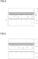
Fig. 2 is a cross-sectional view illustrating a step of forming laser-modified portions. -
Fig. 3 is a cross-sectional view illustrating a step of forming a first wiring layer. -
Fig. 4 is a cross-sectional view illustrating a step of adhering a second support. -
Fig. 5 is a cross-sectional view illustrating a step of releasing a first support. -
Fig. 6 is a cross-sectional view illustrating a step of forming through holes by etching. -
Fig. 7 is a cross-sectional view illustrating a step of forming a second wiring layer. -
Fig. 8 is a cross-sectional view illustrating a step of releasing a second support. -
Fig. 9 is a cross-sectional view of a glass substrate with wiring layers formed on both sides. -
Fig. 10 is a cross-sectional view illustrating a step of forming a build-up layer. -
Fig. 11 is a cross-sectional view of a completed multilayer wiring board. -
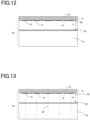
Fig. 12 is a cross-sectional view illustrating a step of forming a wiring layer in a second embodiment. -
Fig. 13 is a cross-sectional view illustrating a step of forming laser-modified portions in the second embodiment. -
Fig. 14 is a cross-sectional view illustrating a step of adhering a second support in a third embodiment. -
Fig. 15 is a cross-sectional view illustrating a step of forming laser-modified portions in the third embodiment. -
Fig. 16 is a cross-sectional view of a multilayer wiring board produced in the first to third embodiments. -
Fig. 17 is a cross-sectional view of a multilayer wiring board produced in the first to third embodiments. -
Fig. 18 is a cross-sectional view illustrating the shape of a through hole produced in the first to third embodiments. -
Fig. 19 is a cross-sectional view of a glass multilayer wiring board for passive components with built-in capacitor structures. -
Fig. 20 is a cross-sectional view of a structure in which an interposer on which a plurality of semiconductor elements are mounted is mounted on a BGA substrate. - With reference to the drawings, some embodiments of the present invention will be described.
- It should be noted that the description below relates to examples of the present invention, and the invention is not limited by these examples. In the following description of the drawings, the same components are denoted by the same reference signs.
- In order to facilitate understanding of the invention, the position, size, shape, range, and the like of each component shown in the drawings may not represent the actual position, size, shape, range, and the like. Therefore, the present invention is not necessarily limited to the position, size, shape, range, and the like disclosed in the drawings.
- The "surface" described herein may refer not only to a surface of a plate-like member, but also to an interface of layers included in the plate-like member, the layers being substantially parallel to the surface of the plate-like member. Further, the "upper surface" and "lower surface" refer to surfaces shown on the upper side and lower side of the plate-like member or the layers included in the plate-like member as viewed in the drawings. In addition, the "upper surface" and "lower surface" may also be called "first surface" and "second surface", respectively.
- The "side surface" refers to a portion extending across the thickness of the surface or layer of the plate-like member or the layers included in the plate-like member. Further, a part of the surface and the side surface may also be collectively referred to as an "end portion".
"Upper" refers to the upper side in the vertical direction when the plate-like member or the layers are placed horizontally. Further, "upper" and "lower" may also be referred to as the "positive Z-axis direction" and "negative Z axis direction", respectively, which are opposite directions, and the horizontal direction may also be referred to as "X axis direction" or "Y axis direction". - The "planar shape" and "plan view" refer to the shape when the surface or layer is viewed from above. Further, the "cross-sectional shape" and "cross-sectional view" refer to the shape as viewed in the horizontal direction when the plate-like member or the layers are cut in a specific direction.
- The "center portion" refers to a center portion other than the peripheral portion of the surface or layer. The "center direction" refers to a direction from the peripheral portion of the surface or layer toward the center of the planar shape of the surface or layer.
- With reference to
Figs. 1 to 11 , a method of producing a multilayer wiring layer in a first embodiment will be described. - First, referring to
Fig. 1 , a step of adhering afirst support 61 to aglass substrate 60 will be described. - As shown in
Fig. 1 , thefirst support 61 is bonded to theglass substrate 60 using a firstadhesive layer 62 to form alaminate structure 63 composed of theglass substrate 60, the firstadhesive layer 62 and thefirst support 61. - The first
adhesive layer 62 is for temporary fixation of thefirst support 61 to theglass substrate 60. Therefore, the material of the firstadhesive layer 62 can be appropriately selected from resins that become releasable by heat generation, sublimation or alteration when absorbing light such as UV light, resins that become releasable by foaming due to heat, resins that become releasable due to the presence of functional groups, and the like. - The first support can be bonded to the
glass substrate 60 using, for example, a laminator, a vacuum pressure press, a vacuum laminator, or the like. - The
first support 61 is preferably made of the same material as that of theglass substrate 60. When theglass substrate 60 is made of alkali-free glass, thefirst support 61 is also preferably made of alkali-free glass. Further, the thickness of the first support can be appropriately set according to the thickness of theglass substrate 60. However, the thickness is preferably a thickness that can be transported during production steps, and ranges from 300 µm to 1,500 µm. - Next, referring to
Fig. 2 , a step of forming laser-modified portions will be described. As shown inFig. 2 , thelaminate structure 63 is irradiated with a laser to form laser-modifiedportions 65 that serve as starting points of through holes. The laser-modifiedportions 65 may extend, for example, in a direction perpendicular to theglass substrate 60, and can be formed substantially over the entire surface of theglass substrate 60. Here, the laser-modifiedportions 65 may also be formed in the firstadhesive layer 62 and thefirst support 61. - In the present embodiment, by irradiating the
glass substrate 60 on which thefirst support 61 is laminated, it is possible to widen the process window for laser irradiation and reliably form desired laser-modified portions in theglass substrate 60. - Next, referring to
Fig. 3 , a step of forming afirst wiring layer 21 will be described. As shown inFig. 3 , thefirst wiring layer 21 including a conductive layer and an insulating resin layer is formed on afirst surface 20, which is an upper surface of theglass substrate 60 of thelaminate structure 63. Specifically, after a seed layer including a hydrofluoric acidresistant metal layer 15 is formed on theglass substrate 60, through-electrode connecting sections 41 andwirings 16 between the through-electrodes are formed on thefirst surface 20 by a semi-additive process (SAP), and an unnecessary seed layer is removed to thereby form an insulatingresin layer 25. - The hydrofluoric acid
resistant metal layer 15 on theglass substrate 60 is an alloy layer made of chromium, nickel or both, and can be formed by sputtering in the range of 10 nm to 1,000 nm. Then, a conductive metallic film is formed on the hydrofluoric acid resistant metal at a desired thickness. The conductive metallic film may be appropriately selected from, for example, Cu, Ni, Al, Ti, Cr, Mo, W, Ta, Au, Ir, Ru, Pd, Pt, AlSi, AlSiCu, AlCu, NiFe, ITO, IZO, AZO, ZnO, PZT, TiN and Cu3N4. - In formation of the first wiring layer by a semi-additive process, a photoresist can be used to form a desired pattern. A dry film resist is typically used, but a liquid resist may be used. After the desired pattern is formed by exposure and development, a plating film of 2 µm or greater and 20 µm or less is formed by electrolytic plating, unnecessary resist pattern is removed, and the seed layer is etched to thereby form wirings.
- The insulating
resin layer 25 is a material containing at least one of epoxy resin, polyimide resin and polyamide resin, and containing fillers such as silica, titanium oxide and urethane, and is preferably a material in the form of liquid or film. A liquid resin can be applied by spin coating, and a film resin can be applied by heating and pressurizing under vacuum using a vacuum laminator. The material of the insulatingresin layer 25 can be appropriately selected as necessary. - Next, referring to
Fig. 4 , a step of adhering a second support will be described. As shown inFig. 4 , a secondadhesive layer 71 and asecond support 70 are formed on thefirst wiring layer 21 of thelaminate structure 63. - The material of the second
adhesive layer 71 can be appropriately selected, as with the firstadhesive layer 62, from resins that become releasable by heat generation, sublimation or alteration when absorbing light such as UV light, resins that become releasable by foaming due to heat, resins having functional groups that temporarily fix theglass substrate 60 to thefirst support 61, and the like, but is preferably different from the material of the firstadhesive layer 62. - The
second support 70 is preferably made of glass, and the same material as that of theglass substrate 60. When theglass substrate 60 is made of alkali-free glass, thefirst support 61 is also preferably made of alkali-free glass. Further, the thickness of the second support can be appropriately set according to the thickness of theglass substrate 60. However, the thickness is preferably a thickness that can be transported, and ranges from 300 µm to 1,500 µm. - Next, referring to
Fig. 5 , a step of releasing the first support will be described. As shown inFig. 5 , the firstadhesive layer 62 and thefirst support 61 are released from the interface between theglass substrate 60 and the firstadhesive layer 62. - In release of the
first support 61 from the interface between theglass substrate 60 and the firstadhesive layer 62, an appropriate release method is selected from UV light irradiation, heating, physical release, and the like depending on the material used for the first adhesive layer. Further, when residues of the firstadhesive layer 62 are present on the bonding surface between theglass substrate 60 and the firstadhesive layer 62, plasma cleaning, ultrasonic cleaning, water cleaning, solvent cleaning using alcohol, or the like may be performed. - Next, with reference to
Fig. 6 , a step of forming through holes by etching will be described. As shown inFig. 6 , the laser-modifiedportions 65 of theglass substrate 60 are selectively removed by etching to form throughholes 12 from the surface on the lower side in the figure. Wet etching with a hydrogen fluoride aqueous solution is suitable for the etching. The amount of etching with hydrogen fluoride aqueous solution is appropriately set according to the thickness of the glass multilayer wiring board. For example, when theglass substrate 60 has a thickness T1 of 200 µm, the amount of etching is preferably in the range of 50 µm or greater and 175 µm or less. - A thickness T2, which is the thickness of the etched
glass substrate 60, is preferably in the range of 25 µm or greater and 150 µm or less. - Next, referring to
Fig. 7 , a step of forming a second wiring layer will be described. As shown inFig. 7 , asecond wiring layer 22 including a conductive layer and an insulating resin layer is formed on asecond surface 30 on a lower side of theglass substrate 60. In formation of the throughholes 12 and the second wiring layer on the second surface of theglass substrate 60, a seed layer for power feeding is formed, a pattern is formed using a resist, plating at 2 µm or more and 20 µm or less is performed, unnecessary resist pattern is removed, and the seed layer is removed to thereby form an insulating resin. - Since the
second wiring layer 22 is not subjected to etching with a hydrogen fluoride aqueous solution in subsequent steps, a material different from the hydrofluoric acid resistant metal can be used. In this case, a metal layer made of a material different from the hydrofluoric acid resistant metal is formed on the side surfaces of the through holes 12. Examples of the material different from the hydrofluoric acid resistant metal include Ti, Cu, and the like, and at least one metal layer made of these materials is formed on the side surfaces of the throughholes 12 and on thesecond surface 30 of theglass substrate 60. The materials, the number of layers, and the like are not limited to the above, and may be appropriately set as necessary. - Next, referring to
Fig. 8 , a step of releasing the second support will be described. As shown inFig. 8 , the secondadhesive layer 71 and thesecond support 70 formed on the upper side of thefirst wiring layer 21 on thefirst surface 20 of theglass substrate 60 are released from the interface between thefirst wiring layer 21 on the first surface and the secondadhesive layer 71. Accordingly, as shown inFig. 9 , theglass substrate 60 with thefirst wiring layer 21 on thefirst surface 20 of theglass substrate 60 and thesecond wiring layer 22 on thesecond surface 30 is obtained. - In release of the
second support 70 from thesecond wiring layer 22, an appropriate release method is selected from UV light irradiation, heating, physical release, and the like depending on the material used for the secondadhesive layer 71. Further, when residues of the secondadhesive layer 71 are present on the bonding surface between thefirst wiring layer 21 and the secondadhesive layer 71, plasma cleaning, ultrasonic cleaning, water cleaning, solvent cleaning using alcohol, or the like may be performed. - Next, referring to
Fig. 10 , a step of forming a build-up layer will be described. - As shown in
Fig. 10 ,conductive electrodes 31 andconductive electrodes 32 are formed in thefirst wiring layer 21 on thefirst surface 20 of theglass substrate 60 and thesecond wiring layer 22 on thesecond surface 30 to electrically connect the first wiring layer on the first surface and the second wiring layer on the second surface, respectively. Theconductive electrodes resin layer 25 by laser irradiation, forming a seed layer on the vias, and then performing a semi-additive process (resist pattern formation, plating, resist removal, seed layer removal, insulating resin layer 25). - At least one layer of each of the
first wiring layer 21 andsecond wiring layer 22 are laminated, and the number of layers can be appropriately set as necessary. - The laser used to form the
conductive electrodes 31 and theconductive electrodes 32 is different from the laser used to form the laser-modifiedportions 65. For example, a pulse laser such as a carbon dioxide gas laser or a UV-YAG laser is preferably used, and a µs pulse width laser is suitable. - Next, as shown in
Fig. 11 , after an outer layer protective film such as a solder resist 55 is formed on each of thefirst wiring layer 21 and thesecond wiring layer 22, semiconductorelement bonding pads 51 andsubstrate bonding pads 53 are subjected to surface treatment such as Ni/Au, Ni/Pd/Au, IT, OSP (water soluble preflux), or the like to form semiconductorelement bonding solder 52 andsubstrate bonding solder 54 as necessary, whereby the multilayer wiring board is completed. - Next, referring to
Figs. 1 ,12 ,13 and4 to 11 , a second embodiment will be described. - The second embodiment differs from the first embodiment in that the laser modification step is performed after forming the first wiring layer.
- In the following description, components that are the same or equivalent to those in the first embodiment described above are denoted by the same reference signs, and the description thereof will be simplified or omitted.
- In a method of producing a multilayer wiring board according to the second embodiment, a step of adhering a first support, which is a first step, is the same as that in the first embodiment described referring to
Fig. 1 , so the description thereof will be omitted. - Next, referring to
Fig. 12 , a step of forming a wiring layer in the second embodiment will be described. - In the second embodiment, subsequent to the step of adhering a first support, a
first wiring layer 21 is formed on theglass substrate 60 of thelaminate structure 63 as shown inFig. 12 . Specifically, after a seed layer including a hydrofluoric acidresistant metal layer 15 is formed on theglass substrate 60, through-electrode connecting sections 41 andwirings 16 between the through-electrodes are formed by a semi-additive process (SAP), and an unnecessary seed layer is removed to thereby form an insulatingresin layer 25. - The materials and film formation methods for the hydrofluoric acid resistant metal layer and the conductive metallic film are the same as those in the first embodiment.
- Next, referring to
Fig. 13 , a step of forming laser-modified portions in the second embodiment will be described. As shown inFig. 13 , a surface of thefirst support 61 of thelaminate structure 63 is irradiated with a laser to form laser-modifiedportions 65 that serve as starting points of through holes. The laser-modifiedportions 65 may extend, for example, in a direction perpendicular to theglass substrate 60, and are formed over the entire surface of theglass substrate 60. Here, the laser-modifiedportions 65 may also be formed in the firstadhesive layer 62 and thefirst support 61. - In the second embodiment, steps subsequent to adhesion of the second support, that is, release of the first support, formation of the through holes by etching, formation of the second wiring layer, release of the second support, and formation of the build-up layer, are the same as those in the first embodiment described referring to
Figs. 4 to 11 , so the description thereof will be omitted. - Next, referring to
Figs. 1 ,12 ,14, 15 and5 to 11 , a third embodiment will be described. - The third embodiment differs from the second embodiment in that the laser modification step is performed after adhering the second support.
- In the following description, components that are the same or equivalent to those in the first and second embodiments described above are denoted by the same reference signs, and the description thereof will be simplified or omitted.
- In a method of producing a glass multilayer wiring board according to the third embodiment, a step of adhering a first support, which is a first step, and a step of forming a first wiring layer are the same as those in the second embodiment described referring to
Figs. 1 and12 , so the description thereof will be omitted. - Next, referring to
Fig. 14 , a step of adhering a second support in the third embodiment will be described. - In the third embodiment, as shown in
Fig. 14 , a secondadhesive layer 71 and asecond support 70 are formed on thefirst wiring layer 21 of thelaminate structure 63. - Then, as shown in
Fig. 15 , thelaminate structure 63 is irradiated with a laser to form laser-modifiedportions 65 that serve as starting points of through holes. The laser-modifiedportions 65 may extend, for example, in a direction perpendicular to theglass substrate 60, and are formed over the entire surface of theglass substrate 60. Here, the laser-modifiedportions 65 may also be formed in the firstadhesive layer 62 and thefirst support 61. - In the third embodiment, steps subsequent to release of the first support, that is, formation of the through holes by etching, formation of the second wiring layer, release of the second support, and formation of the build-up layer, are the same as those in the first embodiment described referring to
Figs. 5 to 11 , so the description thereof will be omitted. - According to the production methods described in the first to third embodiments, not only the
glass substrate 60, but also the support made of the same material as that of theglass substrate 60 are always irradiated with a laser to form laser-modified portions. Therefore, the laser-modified portions can be reliably formed across the entire thickness (z axis direction) of theglass substrate 60. That is, ends of the laser-modified portions, which are portions in which laser modification may be insufficient, are located in the support. Such unstable laser-modified portions are released and removed together with the support in a later step. As a result, the laser-modified portions formed in theglass substrate 60 are highly uniform and precise, and subsequent etching can form uniform through holes. - In the conventional technique, in which only the
glass substrate 60 is irradiated with a laser, the laser-modified portions near the surface of the glass substrate are not necessarily uniform, resulting in variations in the shape of the through holes. However, according to the method of forming a multilayer wiring of the present disclosure, this can be greatly improved. - Referring to
Figs. 16, 17 and18 , the structure of the multilayer wiring boards produced in the first, second and third embodiments will be described. - In the multilayer wiring boards produced in the first to third embodiments of the present invention, the
first wiring layer 21 on thefirst surface 20 of theglass substrate 60 and thesecond wiring layer 22 on thesecond surface 30 are electrically connected to each other via through-electrodes 11 having a frusto-conical shape as shown inFigs. 16, 17 and18 . - The
first wiring layer 21 on thefirst surface 20 and the through-electrodes 11 have a structure in which the through-electrodes 11 are closed by the through-electrode connecting sections 41 of thefirst wiring layer 21 on thefirst surface 20, with the hydrofluoric acidresistant metal layer 15 sandwiched between the through-electrode connecting sections 41 and the through-electrodes 11. - The
conductive electrodes 31 connecting thefirst wiring layer 21 on thefirst surface 20 are formed on the through-electrode connecting sections 41 of the first wiring layer on thefirst surface 20. Theconductive electrodes 32 connecting thesecond wiring layer 22 on thesecond surface 30 are formed at positions away from the through-electrodes 11. Theconductive electrodes 31 connecting thefirst wiring layer 21 on thefirst surface 20 can be formed on the through-electrodes 11 by forming thefirst wiring layer 21 on thefirst surface 20 of theglass substrate 60 and then forming the throughholes 12 by etching, whereby thewirings 16 can be formed between the through-electrodes 11 in the first wiring layer on the first surface. Thefirst wiring layer 21 on the first surface has a higher degree of freedom in wiring design than thesecond wiring layer 22 on the second surface. - Further, according to the present invention, an aperture diameter D2 in the
second wiring layer 22 on thesecond surface 30 can be stably formed, preventing problems of the aperture diameter D2 being reduced. As shown inFig. 18 , in the throughholes 12, that is, the through-electrodes 11, the relationship between an aperture diameter D1 in thefirst wiring layer 21 on thefirst surface 20 of theglass substrate 60 and the aperture diameter D2 in thesecond wiring layer 22 on thesecond surface 30 is D2>D1, and when the aperture diameter D1 onfirst surface 20/aperture D2 on the second surface is in the range of approximately 0.3 to 0.8, it is possible to ensure the throwing power of the seed layer on the side surface and bottom of the through-electrodes 11. This ensures adhesiveness on the side surface and bottom of the through-electrodes 11, resulting in high bonding reliability - The above-mentioned methods of producing a glass multilayer wiring board using a thin glass with a glass thickness of 150 µm or less can be used for devices such as a glass multilayer wiring board for passive components with built-in capacitor structures as shown in
Fig. 19 and an interposer on which a plurality of semiconductor elements are mounted as shown inFig. 20 . The present embodiment, which facilitates the use of a thin glass with a glass thickness of 150 µm or less and makes it possible to easily form through holes and through-electrodes, can be used for various devices that use a glass multilayer wiring board having through-electrodes. - The present invention includes multilayer wiring boards produced by the above-mentioned methods of producing a multilayer wiring board.
- In the multilayer wiring board produced by the production method described in
PTL 1, the first surface-side aperture diameters of apertures of the holes and the second surface-side aperture diameters of apertures of the holes are in the range of approximately ±15% to ±20% from their respective average values. On the other hand, in the multilayer wiring board produced by the production method of the present invention, the first surface-side aperture diameters of apertures of the holes and the second surface-side aperture diameters of apertures of the holes are within around ±5% from their respective average values. Therefore, the present invention includes a multilayer wiring board including a glass substrate having a first surface and a second surface, the glass substrate having holes penetrating between the first surface and the second surface, wherein the first surface-side aperture diameters of apertures of the holes and the second surface-side aperture diameters of apertures of the holes are within ±10% from their respective average values. - Further, as described above, the present invention includes a multilayer wiring board, wherein one of the average values of the first surface-side aperture diameters of the apertures of the holes and the second surface-side aperture diameters of the apertures of the holes is smaller than the other, and a ratio between the average values is 0.3 or greater and 0.8 or less.
- Further, the present invention includes a multilayer wiring board, wherein the first surface-side apertures of the holes or the second surface-side apertures of the holes, whichever is smaller in aperture diameter, are at least partially closed by a film structure made of a material resistant to hydrofluoric acid corrosion (for example, hydrofluoric acid resistant metal layer 15).
- The scope of the present invention is not limited to the example embodiments shown and described, but includes various modifications. For example, the above embodiments have been described in detail in order to facilitate understanding of the present invention, but the present invention is not necessarily limited to those having all the configurations described.
- Further, some of the configurations of one embodiment can be replaced with a configuration of another embodiment, and a configuration of one embodiment can include a configuration of one or more other embodiments. Further, some of the configurations of each embodiment can be added, deleted or replaced with other configurations.
- Furthermore, the present invention includes all embodiments that provide effects equivalent to those intended by the present invention.
-
- 1: Glass multilayer wiring board,
- 11: Through electrode,
- 12: Through hole,
- 15: Hydrofluoric acid resistant metal layer,
- 16: Wiring,
- 21: First wiring layer,
- 22: Second wiring layer,
- 25: Insulating resin layer,
- 31: Conductive electrode,
- 32: Conductive electrode,
- 41: Through electrode connecting section,
- 42: Through electrode connecting section,
- 51: Semiconductor element bonding pad,
- 52: Semiconductor element bonding solder,
- 53: Substrate bonding pad,
- 54: Substrate bonding solder,
- 55: Solder resist,
- 60: Glass substrate,
- 61: First support,
- 62: First adhesive layer,
- 63: Laminate structure,
- 65: Laser-modified portion,
- 70: Second support,
- 71: Second adhesive layer,
- 80: Capacitor structure,
- 90: BGA substrate,
- 100: Semiconductor element,
- D1: First surface-side aperture diameter of through hole
- D2: Second surface-side aperture diameter of through hole
Claims (9)
- A method of producing a multilayer wiring board including a glass substrate having through holes, the glass substrate having a first surface and a second surface, the method comprising:a first step of adhering a first support made of glass to the second surface of the glass substrate;a second step of forming modified portions in the glass substrate and the first support by laser irradiation;a third step of releasing and removing the first support; anda fourth step of forming through holes in the glass substrate by etching.
- The method of producing a multilayer wiring board according to claim 1, wherein
the second step of forming modified portions is performed after forming a first wiring layer on the first surface of the glass substrate. - The method of producing a multilayer wiring board according to claim 1, wherein
the second step of forming modified portions is performed after forming a first wiring layer on an upper side of the first surface of the glass substrate and adhering a second support to an upper side of the first wiring layer. - The method of producing a multilayer wiring board according to any one of claims 1 to 3, further comprising:after the fourth step of forming through holes, a fifth step of forming a second wiring layer on a lower side of the second surface of the glass substrate from which the first support has been released and removed; anda sixth step of releasing and removing the second support.
- The method of producing a multilayer wiring board according to claim 4, further comprising:after the sixth step of releasing and removing the second support,a step of forming a build-up layer on an upper side and/or a lower side of the glass substrate.
- A multilayer wiring board produced by the method of producing a multilayer wiring board according any one of claims 1 to 5.
- A multilayer wiring board comprising a glass substrate having a first surface and a second surface, the glass substrate having holes penetrating between the first surface and the second surface, wherein
first surface-side aperture diameters of apertures of the holes and second surface-side aperture diameters of apertures of the holes are within ±10% from their respective average values. - The multilayer wiring board according to claim 7, wherein
one of the average values of the first surface-side aperture diameters of the apertures of the holes and the second surface-side aperture diameters of the apertures of the holes is smaller than the other, and a ratio between the average values is 0.3 or greater and 0.8 or less. - The multilayer wiring board according to claim 8, wherein
the first surface-side apertures of the holes or the second surface-side apertures of the holes, whichever is smaller in aperture diameter, are at least partially closed by a film structure made of a material resistant to hydrofluoric acid corrosion.
Applications Claiming Priority (2)
| Application Number | Priority Date | Filing Date | Title |
|---|---|---|---|
| JP2021194330A JP7067666B1 (en) | 2021-11-30 | 2021-11-30 | Manufacturing method of multi-layer wiring board |
| PCT/JP2022/041103 WO2023100586A1 (en) | 2021-11-30 | 2022-11-04 | Multilayer wiring board manufacturing method, and multilayer wiring board |
Publications (2)
| Publication Number | Publication Date |
|---|---|
| EP4444049A1 true EP4444049A1 (en) | 2024-10-09 |
| EP4444049A4 EP4444049A4 (en) | 2025-03-05 |
Family
ID=81606842
Family Applications (1)
| Application Number | Title | Priority Date | Filing Date |
|---|---|---|---|
| EP22901019.4A Pending EP4444049A4 (en) | 2021-11-30 | 2022-11-04 | METHOD FOR MANUFACTURING MULTILAYER WIRING BOARD, AND MULTILAYER WIRING BOARD |
Country Status (6)
| Country | Link |
|---|---|
| US (1) | US20240312797A1 (en) |
| EP (1) | EP4444049A4 (en) |
| JP (2) | JP7067666B1 (en) |
| CN (1) | CN118383087A (en) |
| TW (1) | TW202332350A (en) |
| WO (1) | WO2023100586A1 (en) |
Families Citing this family (11)
| Publication number | Priority date | Publication date | Assignee | Title |
|---|---|---|---|---|
| CN115190695A (en) * | 2022-05-20 | 2022-10-14 | 长沙汇意圆科技有限公司 | Glass substrate double-side conduction microcircuit processing method |
| WO2024004566A1 (en) * | 2022-07-01 | 2024-01-04 | Toppanホールディングス株式会社 | Glass core laminate structure and production method for glass core laminate structure |
| JP2024014262A (en) * | 2022-07-22 | 2024-02-01 | Toppanホールディングス株式会社 | Multilayer wiring board manufacturing method |
| JP2024046350A (en) * | 2022-09-22 | 2024-04-03 | Toppanホールディングス株式会社 | Wiring Board |
| JP2024062685A (en) * | 2022-10-25 | 2024-05-10 | Toppanホールディングス株式会社 | Method for manufacturing wiring board |
| JP2024062689A (en) * | 2022-10-25 | 2024-05-10 | Toppanホールディングス株式会社 | Method for manufacturing wiring board |
| JP2024071115A (en) * | 2022-11-14 | 2024-05-24 | Toppanホールディングス株式会社 | Wiring board and method for manufacturing the same |
| US20240217216A1 (en) * | 2022-12-29 | 2024-07-04 | Intel Corporation | Ultrathin laminated glass and glass stiffeners for coreless packages |
| CN117976550A (en) * | 2024-03-28 | 2024-05-03 | 深圳市矩阵多元科技有限公司 | Substrate manufacturing method and substrate |
| US12315788B1 (en) * | 2024-04-30 | 2025-05-27 | Dyi-chung Hu | Semiconductor substrate and manufacturing method thereof |
| CN119252818A (en) * | 2024-09-29 | 2025-01-03 | 成都奕成集成电路有限公司 | Chip packaging structure and chip packaging method |
Family Cites Families (9)
| Publication number | Priority date | Publication date | Assignee | Title |
|---|---|---|---|---|
| EP2925482A1 (en) * | 2012-11-29 | 2015-10-07 | Corning Incorporated | Sacrificial cover layers for laser drilling substrates and methods thereof |
| KR20170139680A (en) | 2015-04-28 | 2017-12-19 | 코닝 인코포레이티드 | A method of laser drilling a through hole in a substrate using an exit sacrificial cover layer and a method of laser drilling a through hole |
| JP6571437B2 (en) * | 2015-07-29 | 2019-09-04 | リンテック株式会社 | Manufacturing method of semiconductor device |
| WO2018092480A1 (en) * | 2016-11-17 | 2018-05-24 | 大日本印刷株式会社 | Through-electrode substrate, semiconductor device using through-electrode substrate, and through-electrode substrate manufacturing method |
| US11078112B2 (en) * | 2017-05-25 | 2021-08-03 | Corning Incorporated | Silica-containing substrates with vias having an axially variable sidewall taper and methods for forming the same |
| CN112335037B (en) * | 2018-06-08 | 2024-11-26 | 凸版印刷株式会社 | Method for manufacturing glass device and glass device |
| WO2020100308A1 (en) | 2018-11-16 | 2020-05-22 | 日立化成株式会社 | Semiconductor device and manufacturing method thereof, and structure used in manufacture of semiconductor device |
| JP7242362B2 (en) | 2019-03-18 | 2023-03-20 | キオクシア株式会社 | Semiconductor device manufacturing method |
| JP7409031B2 (en) * | 2019-11-18 | 2024-01-09 | Toppanホールディングス株式会社 | Glass core multilayer wiring board and its manufacturing method |
-
2021
- 2021-11-30 JP JP2021194330A patent/JP7067666B1/en active Active
-
2022
- 2022-04-28 JP JP2022074110A patent/JP7810056B2/en active Active
- 2022-11-04 EP EP22901019.4A patent/EP4444049A4/en active Pending
- 2022-11-04 CN CN202280077771.3A patent/CN118383087A/en active Pending
- 2022-11-04 WO PCT/JP2022/041103 patent/WO2023100586A1/en not_active Ceased
- 2022-11-29 TW TW111145571A patent/TW202332350A/en unknown
-
2024
- 2024-05-29 US US18/676,821 patent/US20240312797A1/en active Pending
Also Published As
| Publication number | Publication date |
|---|---|
| US20240312797A1 (en) | 2024-09-19 |
| TW202332350A (en) | 2023-08-01 |
| JP7067666B1 (en) | 2022-05-16 |
| JP7810056B2 (en) | 2026-02-03 |
| CN118383087A (en) | 2024-07-23 |
| EP4444049A4 (en) | 2025-03-05 |
| JP2023081264A (en) | 2023-06-09 |
| WO2023100586A1 (en) | 2023-06-08 |
| JP2023080810A (en) | 2023-06-09 |
Similar Documents
| Publication | Publication Date | Title |
|---|---|---|
| US20240312797A1 (en) | Methods of producing multilayer wiring boards, and multilayer wiring boards | |
| US10383228B2 (en) | Electronic component device and method for manufacturing the same | |
| US20210118698A1 (en) | Method for manufacturing glass device, and glass device | |
| US9763332B2 (en) | Support body, method of manufacturing support body, method of manufacturing wiring board, method of manufacturing electronic component, and wiring structure | |
| US7761982B2 (en) | Method for manufacturing IC-embedded substrate | |
| US9418928B2 (en) | Protrusion bump pads for bond-on-trace processing | |
| JP2000106482A (en) | Flexible substrate manufacturing method | |
| JP2018032657A (en) | Printed wiring board and printed wiring board manufacturing method | |
| US20250125272A1 (en) | Glass core laminate structure and production method for glass core laminate structure | |
| JP2013083620A (en) | Probe card and manufacturing method thereof | |
| WO2024062808A1 (en) | Wiring substrate | |
| US20250261302A1 (en) | Wiring substrate and manufacturing method of wiring substrate | |
| JP2020161572A (en) | Wiring board and manufacturing method of wiring board | |
| JP7740427B2 (en) | Wiring board and method for manufacturing the same | |
| JP4097310B2 (en) | Multilayer circuit board manufacturing method | |
| JP2024146315A (en) | Wiring board and method for manufacturing the same | |
| JP2024009740A (en) | Multilayer wiring board and its manufacturing method | |
| JP2024062689A (en) | Method for manufacturing wiring board | |
| KR20240063896A (en) | Substrates and semiconductor devices with attached supports | |
| JP2024014262A (en) | Multilayer wiring board manufacturing method | |
| JP2024062685A (en) | Method for manufacturing wiring board | |
| WO2024161912A1 (en) | Interposer, semiconductor package, and methods for manufacturing same | |
| JP2024093745A (en) | Method for manufacturing wiring board | |
| WO2026058684A1 (en) | Interposer and semiconductor package | |
| JP4398550B2 (en) | Bumped multilayer substrate manufacturing method |
Legal Events
| Date | Code | Title | Description |
|---|---|---|---|
| STAA | Information on the status of an ep patent application or granted ep patent |
Free format text: STATUS: THE INTERNATIONAL PUBLICATION HAS BEEN MADE |
|
| PUAI | Public reference made under article 153(3) epc to a published international application that has entered the european phase |
Free format text: ORIGINAL CODE: 0009012 |
|
| STAA | Information on the status of an ep patent application or granted ep patent |
Free format text: STATUS: REQUEST FOR EXAMINATION WAS MADE |
|
| 17P | Request for examination filed |
Effective date: 20240328 |
|
| AK | Designated contracting states |
Kind code of ref document: A1 Designated state(s): AL AT BE BG CH CY CZ DE DK EE ES FI FR GB GR HR HU IE IS IT LI LT LU LV MC ME MK MT NL NO PL PT RO RS SE SI SK SM TR |
|
| A4 | Supplementary search report drawn up and despatched |
Effective date: 20250204 |
|
| DAV | Request for validation of the european patent (deleted) | ||
| DAX | Request for extension of the european patent (deleted) | ||
| RIC1 | Information provided on ipc code assigned before grant |
Ipc: H05K 1/03 20060101ALN20250129BHEP Ipc: H05K 1/11 20060101ALN20250129BHEP Ipc: H05K 3/00 20060101ALN20250129BHEP Ipc: H01L 23/498 20060101ALI20250129BHEP Ipc: H01L 23/15 20060101ALI20250129BHEP Ipc: H01L 21/48 20060101ALI20250129BHEP Ipc: H01L 21/683 20060101ALI20250129BHEP Ipc: H05K 3/42 20060101ALI20250129BHEP Ipc: H05K 3/46 20060101AFI20250129BHEP |
|
| STAA | Information on the status of an ep patent application or granted ep patent |
Free format text: STATUS: EXAMINATION IS IN PROGRESS |
|
| 17Q | First examination report despatched |
Effective date: 20250822 |