EP4436075A2 - Kreuzpunktschalter mit ¢led-io-ports und abbildungsfaserkabeln - Google Patents
Kreuzpunktschalter mit ¢led-io-ports und abbildungsfaserkabeln Download PDFInfo
- Publication number
- EP4436075A2 EP4436075A2 EP24193949.5A EP24193949A EP4436075A2 EP 4436075 A2 EP4436075 A2 EP 4436075A2 EP 24193949 A EP24193949 A EP 24193949A EP 4436075 A2 EP4436075 A2 EP 4436075A2
- Authority
- EP
- European Patent Office
- Prior art keywords
- input
- output
- ports
- fiber
- port
- Prior art date
- Legal status (The legal status is an assumption and is not a legal conclusion. Google has not performed a legal analysis and makes no representation as to the accuracy of the status listed.)
- Pending
Links
Images


Classifications
-
- G—PHYSICS
- G02—OPTICS
- G02B—OPTICAL ELEMENTS, SYSTEMS OR APPARATUS
- G02B6/00—Light guides; Structural details of arrangements comprising light guides and other optical elements, e.g. couplings
- G02B6/04—Light guides; Structural details of arrangements comprising light guides and other optical elements, e.g. couplings formed by bundles of fibres
- G02B6/06—Light guides; Structural details of arrangements comprising light guides and other optical elements, e.g. couplings formed by bundles of fibres the relative position of the fibres being the same at both ends, e.g. for transporting images
-
- G—PHYSICS
- G02—OPTICS
- G02B—OPTICAL ELEMENTS, SYSTEMS OR APPARATUS
- G02B6/00—Light guides; Structural details of arrangements comprising light guides and other optical elements, e.g. couplings
- G02B6/24—Coupling light guides
- G02B6/42—Coupling light guides with opto-electronic elements
- G02B6/4201—Packages, e.g. shape, construction, internal or external details
- G02B6/4246—Bidirectionally operating package structures
-
- G—PHYSICS
- G02—OPTICS
- G02B—OPTICAL ELEMENTS, SYSTEMS OR APPARATUS
- G02B6/00—Light guides; Structural details of arrangements comprising light guides and other optical elements, e.g. couplings
- G02B6/24—Coupling light guides
- G02B6/42—Coupling light guides with opto-electronic elements
- G02B6/4201—Packages, e.g. shape, construction, internal or external details
- G02B6/4249—Packages, e.g. shape, construction, internal or external details comprising arrays of active devices and fibres
-
- G—PHYSICS
- G02—OPTICS
- G02B—OPTICAL ELEMENTS, SYSTEMS OR APPARATUS
- G02B6/00—Light guides; Structural details of arrangements comprising light guides and other optical elements, e.g. couplings
- G02B6/24—Coupling light guides
- G02B6/42—Coupling light guides with opto-electronic elements
- G02B6/43—Arrangements comprising a plurality of opto-electronic elements and associated optical interconnections
-
- H—ELECTRICITY
- H04—ELECTRIC COMMUNICATION TECHNIQUE
- H04B—TRANSMISSION
- H04B10/00—Transmission systems employing electromagnetic waves other than radio-waves, e.g. infrared, visible or ultraviolet light, or employing corpuscular radiation, e.g. quantum communication
- H04B10/25—Arrangements specific to fibre transmission
- H04B10/2581—Multimode transmission
-
- H—ELECTRICITY
- H04—ELECTRIC COMMUNICATION TECHNIQUE
- H04J—MULTIPLEX COMMUNICATION
- H04J14/00—Optical multiplex systems
- H04J14/05—Spatial multiplexing systems
- H04J14/052—Spatial multiplexing systems using multicore fibre
-
- H—ELECTRICITY
- H04—ELECTRIC COMMUNICATION TECHNIQUE
- H04Q—SELECTING
- H04Q11/00—Selecting arrangements for multiplex systems
- H04Q11/0001—Selecting arrangements for multiplex systems using optical switching
- H04Q11/0005—Switch and router aspects
-
- H—ELECTRICITY
- H04—ELECTRIC COMMUNICATION TECHNIQUE
- H04Q—SELECTING
- H04Q11/00—Selecting arrangements for multiplex systems
- H04Q11/0001—Selecting arrangements for multiplex systems using optical switching
- H04Q11/0005—Switch and router aspects
- H04Q2011/0007—Construction
-
- H—ELECTRICITY
- H04—ELECTRIC COMMUNICATION TECHNIQUE
- H04Q—SELECTING
- H04Q11/00—Selecting arrangements for multiplex systems
- H04Q11/0001—Selecting arrangements for multiplex systems using optical switching
- H04Q11/0005—Switch and router aspects
- H04Q2011/0037—Operation
- H04Q2011/0039—Electrical control
Definitions
- the present disclosure generally relates to networking hardware. More particularly, the present disclosure relates to systems and methods for micro-LED/PD arrangements and selection in an optical interconnect over imaging fiber, and for a crosspoint switch with ⁇ LED IO ports and imaging fiber bundle.
- Ten Meter Interconnect represents a new approach in short reach optical transmission.
- short reach optical transmission has been considered for reaches in excess of 100s of meters.
- new approaches redefine short reach optical transmission, where it is now possible to consider it on a scale of meters.
- a 10MI transmitter based on Light-Emitting Diode (LED)
- PD photodetectors
- This imaging fiber (bundle) consists of thousands (or tens of thousands) of fiber cores. The cost of imaging fiber is only marginally higher as number of fiber cores increases, so it can be advantageous to use a single bundle for bidirectional transmission rather than two separate bundles.
- TX transmit
- RX receiver
- LED/PD splits The aspects of alternate splits between TX and RX areas and increased tolerance to angular and X-Y (Cartesian) misalignment by selectable combining of output signals described in this disclosure have not been previously disclosed or practiced
- OCSs Optical Circuit Switches
- the present approach is to adapt the ratios of resource pools to a particular workload: CPU, GPU, Memory, Accelerator, FPGA, and Storage pools.
- a key performance metric is ultra-low latency, which is particularly necessary when the CPU/GPU/TPU pool is physically separate from the Memory pool.
- Some approaches use a combination of tunable lasers and passive gratings that route light based on its wavelength.
- Other OCSs are commonly implemented with micro-mirror MEMS devices but are slow to reconfigure.
- optical switch approaches have several drawbacks, which so far prevented their wide adoption in the industry. Further, none of these optical approaches are compatible with a novel micro-Light Emitting Diode ( ⁇ LED) based optical link technology due to the use of an unusual 'imaging' fiber bundle for transmission and short-wavelength (Blue) sources. ⁇ LEDs combined with imaging fiber provide very low cost, low power optical links. However, it is currently not feasible to optically switch imaging fiber bundles while preserving their spatial coherence properties. What is needed is a corresponding switching fabric that will also provide very low cost, low power approach. Further, electrically-based switching has additional benefits of signal regeneration and very fast (sub-nanosecond) switching.
- an optical transceiver is provided as defined by claim 1.
- the fiber cores are imaging fibers.
- the M transmitters may each be micro Light Emitting Diodes (LEDs) and the P receivers are photodetectors (PDs).
- each of micro light emitting diodes transmits at least 1Gb/s.
- the optical transceiver may further include transmitter circuitry configured to receive an aggregate transmit signal and to cause transmission of the aggregate signal as a plurality of lower rate transmit signals, each by one of the M transmitters over a portion of the first set of the K cores; and receiver circuitry configured to receive a plurality of lower rate transmit signals from the P receivers and to create an aggregate receive signal based thereon.
- the aggregate transmit and the aggregate receive signal may be at least 100Gb/s
- the fiber cable may include a plurality of fiber cores used as guard bands.
- the guard bands may be in both the first set of the K fiber cores between adjacent M transmitters and in the second set of K fiber cores between adjacent P receivers.
- the fiber cable may have a length of 10m or less.
- the first set of the K fiber cores and the second set of the K fiber cores may be fixed.
- the first set of the K fiber cores and the second set of the K fiber cores may be determined during operation based on the fiber cable and associated connections to the optical transceiver.
- the optical transceiver further includes alignment circuitry connected to the M transmitters and the P receivers, wherein the alignment circuitry is configured to select the first set of the K fiber cores and the second set of the K fiber cores.
- the second set of the K fiber cores may be determined based on a limiting parameter including any of i) post transimpedance amplifier (TIA) noise and impact on signal-to-noise ratio (SNR) and ii) direct photodiode photocurrent summation which is limited by photodiode capacitance.
- TIA post transimpedance amplifier
- SNR signal-to-noise ratio
- ii) direct photodiode photocurrent summation which is limited by photodiode capacitance.
- the first set of the K fiber cores and the second set of the K fiber cores may each be about half of the K fiber cores.
- One embodiment is conceived to have first set of the K fiber cores and second set of K fiber cores arranged in half circles.
- the first set of the K fiber cores and the second set of the K fiber cores are each in a circular arrangement with one located in an inner area and one located in an outer ring adjacent to the inner area. K ⁇ 1000.
- an optical switch system includes a plurality of input ports with each input port configured to connect to an input fiber bundle; a plurality of output ports with each output port configured to connect to an output fiber bundle, wherein each of the input fiber bundle and the output fiber bundle include a cable having K fiber cores, K » 1; and an electrical crosspoint switch connected to the plurality of input ports and the plurality of output ports, wherein the electrical crosspoint switch is configured to connect a given input port to a corresponding output port, including all signals in the input fiber bundle to the corresponding output fiber bundle.
- Each input port is a photodiode array and each output port is a light emitting diode array, and wherein the plurality of input ports, the plurality of output ports, and the electrical crosspoint switch are copackaged together.
- the plurality of input ports are in a photodiode array circuit
- the plurality of output ports are in a micro light emitting diode array circuit
- the electrical crosspoint switch is in a switch circuit
- the photodiode array circuit are stacked on the switch circuit.
- the K fiber cores form an imaging fiber.
- Each input port and each output port include a plurality of signals forming an aggregate signal.
- Each output port includes M transmitters, M and K are integers, M ⁇ K, and each input port includes P receivers, P is an integer, P ⁇ K.
- one of the P receivers may be adapted for selecting a destination address in the electrical crosspoint switch.
- one of the P receivers may be adapted for clock phase.
- the electrical crosspoint switch includes a plurality of input traces connected to each input port and a plurality of output traces connected to each output port.
- the plurality of input traces are logically positioned horizontally and the plurality of output traces are logically positioned vertically relative to the plurality of input traces, and wherein the electrical crosspoint switch further includes a plurality of switches at corresponding crossings of the plurality of input traces and the plurality of output traces.
- the plurality of input ports and the plurality of output ports are short reach devices, and further including one or more long reach optical modems connected to one or more of the output ports.
- the short reach devices are few meter modems, and the one or more long reach optical modems are coherent modems.
- the plurality of input ports and the plurality of output ports each include a plurality of data channels, and wherein the plurality of data channels form an aggregate signal for switching via the electrical crosspoint switch.
- Each input port is a photodiode array, and each output port is a laser array.
- a layered electronic crosspoint switch adapted to selectively couple a plurality of input ports and output ports includes a plurality of layered electronic crosspoint switches; a plurality of input ports with each input port configured to connect to an input fiber bundle; and a plurality of output ports with each output port configured to connect to an output fiber bundle.
- Each input port is a photodiode array and each output port is a micro light emitting diode array.
- Each of the input fiber bundle and the output fiber bundle include a cable having fiber cores, wherein the fiber cores are imaging fibers.
- the plurality of input ports and the plurality of output ports each include a plurality of data channels, and wherein the plurality of data channels form an aggregate signal for switching via the electrical crosspoint switch.
- Each of the plurality of layered crosspoint switches are configured for a data channel, wherein one of the layered crosspoint switches may be configured as a clock channel.
- the present disclosure relates to systems and methods for an optical switch system which provides a combination of ⁇ LED arrays, PDs, imaging fiber bundles, and crosspoint switch as a system on a chip module.
- the system includes a plurality of input ports with each input port configured to connect to an input fiber bundle.
- the system additionally includes a plurality of output ports with each output port configured to connect to an output fiber bundle, wherein each of the input fiber bundle and the output fiber bundle include a cable having a plurality of fiber cores.
- An electrical crosspoint switch is connected to the plurality of input ports and the plurality of output ports, wherein the electrical crosspoint switch is configured to connect a given input port to a corresponding output port, including all signals in the input fiber bundle to the corresponding output fiber bundle.
- the present disclosure relates to systems and methods for increasing tolerance to misalignment of optical transceivers.
- Contemplated herein are various partitioning methods of ⁇ LED and PD arrangements which allow for X-Y (Cartesian) and angular insensitivity of fiber alignment.
- additional ⁇ LED and PD devices can be strategically located near split lines (i.e., the border between ⁇ LEDs and PDs) to allow for additional coarse misalignment tolerances.
- Various embodiments include utilizing dark (unilluminated) fiber core guard bands between ⁇ LED devices to increase tolerance to misalignment between ⁇ LEDs, imaging fiber (fiber cores), and PDs.
- Various embodiments include minimizing dead zibes between PDs to increase light collection efficiency.
- the ability to selectively combine signals from multiple PDs greatly improves SNR and thereby link budget. Selection of specific PD groupings is implemented either at manufacturing and fixed, or during operation. If selection of specific PD groupings is done during operation, it should facilitate extensions to connectorized fibers, optical switching, and or external fiber patch cord use with possible angular and Cartesian (X,Y) misalignment.
- a specific efficient procedure for determining the particular grouping of PDs into a single data channel output is also utilized by various embodiments of the present disclosure.
- PD membership in a grouping may be dependent on a limiting parameter. For example, post-TIA summation is limited by TIA noise and its impact on SNR. Direct PD photocurrent summation is limited by PD capacitance and impact on bandwidth. Further, various embodiments include an additional guard band on areas of devices (optical transceivers) that may be either more expensive or more prone to failure.
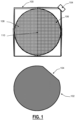
- FIG. 1 is a diagram of the physical alignment features of multicore fiber cables and chips, and describes how the industry achieves this alignment in the production of interconnect cables.
- the fiber bundle has a length of 10m or less.
- FIG. 1 shows a chip (optical transceiver) 100 and fiber bundle 102.
- the chip 100 includes a physical alignment feature 104 disposed on a corner of the chip 100.
- the chip is coupled to a plurality of Light-Emitting Diodes ( ⁇ LEDs) (also referred to as transmitters) 108 and Photodetectors (PDs) (also referred to as receivers) 106 arranged on the surface of the chip 100.
- ⁇ LEDs Light-Emitting Diodes
- PDs Photodetectors
- the ⁇ LEDs 108 and PDs 106 are arranged in a half-circle arrangement which allows for the same type of chip to be used at both ends of the connection.
- the half-circle arrangement requires X and Y axis alignment, as well as angular alignment.
- the fiber bundle 102 also includes a physical alignment feature 104 which is common with image fiber.
- the multicore fiber bundle 102 and chip 100 shown in FIG. 1 requires extra ⁇ LED 108 and PD 106 channels near the split line 110 and closer to the perimeter. Loose alignment tolerancing will require some way to selectively define PD 106 groups during manufacturing, as well as association of groups with
- the ⁇ LEDs 108 of the present disclosure may be any light emitting device such as micro-LEDs, Vertical Cavity Surface Emitting Lasers (VCSELs) or any other device known to one of skill in the art.
- the photodetectors 106 of the present disclosure may be any light detecting device or device for converting photon energy of light into electrical signals known to one of skill in the art.
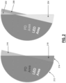
- FIG. 2 illustrates how the present disclosure tolerates up to 9 degrees of angular misalignment with a reasonable number (about 5%) of excess ⁇ LEDs and PDs.
- a training pattern or procedure can identify which ⁇ LEDs need to be disabled.
- FIG. 2 illustrates possible angular misalignment between an ⁇ LED half-circle 212 and PD half-circle 214. The figure shows equal half-circles dedicated to an ⁇ LED to PD connection.
- angular misalignment leads to a sliver of wasted ⁇ LEDs 216 and a sliver of wasted PDs 218. There may be additional wasted PDs 218 along the ⁇ LED boundary due to near-end reflection crosstalk.
- the figure also shows a case where it is desired to save either more expensive or less reliable devices (i.e. ⁇ LED in this example).
- the disclosure provides a guard band 206 of unpopulated area on the ⁇ LED half-circle 212. This is constructed geometrically by creating a chord in the circle that does not pass through the center and thus results in unequal segments. This reduces the sliver of wasted ⁇ LEDs at the expense of increased sliver of wasted PDs.
- various embodiments include a plurality of fiber cores used as guard bands in the fiber cable.
- ⁇ LED channel For all misalignments (X axis, Y axis, and angular), it is advantageous to selectively detect optimal PD groups and associate a group with a specific ⁇ LED channel. Accomplishing this starts by taking advantage of the fact that blue light has a short absorption length in silicon. That enables a low-capacitance PD which in turn enables high-gain in a first TIA (Trans-Impedance Amplifier) stage. This high-gain TIA gives the signal sufficient strength to drive up to 7 analog transmission gates and associated crosspoint stubs. The second TIA stage acts to sum a group of up to 7 PDs into a single channel and drive a flip-flop gate.
- TIA Trans-Impedance Amplifier
- Complementary Metal-Oxide Semiconductor (CMOS) transmission line signal speed can be approximately 1.7E8 m/s, and a 10Gbps signal with a 100ps bit period corresponds to ⁇ 17mm.
- the crosspoint switch is expected to be much smaller and can therefore be considered as a lumped element greatly simplifying overall design and assuring signal integrity without termination.
- the crosspoint switch can have series resistors (including through-gate resistance) with each TIA and act as a voltage adder for up to 7 or more TIAs.
- the signal chain can be implemented with an IA (Current Amplifier) and the switch can act as a current adder.
- the embodiments disclosed herein may include hardware with different operating specifications.
- the ⁇ LEDs are adapted to each transmit at least 1 Gb/s.
- Transmitter circuitry can be configured to receive an aggregate transmit signal to cause transmission of the aggregate signal as a plurality of lower rate transmit signals, each by one of the ⁇ LEDs (transmitters) over a portion of a first set of fiber cores.
- the Receiver circuitry can additionally be configured to receive a plurality of lower rate transmit signals from the PDs (receivers) and create an aggregate receive signal based thereon.
- the aggregate transmit, and the aggregate receive signal are at least 100Gb/s.
- crosspoint switch Although the present disclosure has considered the crosspoint switch as a single large design, it might be necessary to segment it to control the crosstalk impact of parasitic capacitances on open transmission gates. This is done because overlap would be required in the segments to deal with desired tolerance to physical misalignments. For example, a group of PDs near the boundary between cross point segments would have the ability to drive both switch segments. The extra drive strength may be provided by an additional amplifier.
- FIG. 3 and FIG. 4 show a TIA with intermediate analog crosspoint 300.
- each PD 306 is locally integrated with a stage 1 TIA 322.
- 2800 PDs 306 are contemplated with 7 PDs 306 per ⁇ LED resulting in 400 ⁇ LEDs. It will be appreciated that other embodiments may have any number of PDs 306 with any number of ⁇ LEDs, and any number of PDs 306 per ⁇ LED.
- FIG. 4 shows the analog crosspoint switch with transmission gates (2800 inputs, 400 outputs), a training monitor 324, stage 2 signal aggregation 322 which may be either a voltage or a current adder, and flip-flop gate 326.
- a training algorithm periodically recalibrates the PD groupings while in service, this accommodates ⁇ LED failure, aging, temperature, bending, XY axis tolerancing, angular tolerancing, and breakouts.
- the training can also be done only at manufacturing, which can accommodate breakouts and initial tolerancing.
- Training requires ⁇ LEDs to be turned on in separated groups and the resulting signal strength being measured by the PD array at the other end of the fiber.
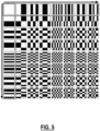
- An efficient way of searching this space is by lighting up the ⁇ LED array using Hadamard patterns (64 such patterns shown in FIG. 5 ). This efficiency is important if done in-service to reduce overhead bandwidth, but also during manufacturing to reduce the cost of tuning time.
- FIG. 6 shows a cross section of an example 3D die stackup 628.
- the die stackup 628 includes a plurality of fiber cores 630, and a cross section of the chip 100 of FIG. 1 , a PCB 636, and packaging substrate 638. Additionally, disposed on the chip 100 are a plurality of lenses 632 oriented over the plurality of ⁇ LEDs 608 and PDs 606. Again, in the present embodiment, the chip 100 includes separated sections 100a and 100b on which the ⁇ LEDs 608 and PDs 606 are disposed.
- these separated sections are constructed as the half-circle sections disclosed herein, while other embodiments provide other shapes and configurations of the sections 100a and 100b on which the ⁇ LEDs 608 and PDs 606 are disposed.
- FIG. 6 shows how the PDs 606 and stage-1 TIAs 622 do not compete for area with the crosspoint switch 634.
- the present embodiment shows the first-stage TIA 622 competing for area with the PD 606 in a planar CMOS process, a TIA located under a back-illuminated PD on the same die is also contemplated so that it doesn't steal light-gathering capacity from the PD.
- the same chip 100 is used at both ends for volume and cost reasons. It is also assumed that the cable is constructed from a group of fiber cores 630 with no particular orientation or alignment necessary between them. The training algorithm detects where the subset of fibers lands on each array, meaning that precise alignment is not necessary.
- FIG. 7 is a diagram of multi core cables aligned over an array (chip) without precise alignment.
- 20 multi core cables 740 are aligned over the plurality ⁇ LEDs 708 disposed on the chip 100 (transmitting chip) with 4 separate groups of 5 multi core cables 740 transmitting to 4 different receiving (RX) chips 742. More specifically, the groups of cables 740 are transmitting light from the ⁇ LEDs 708 of the first chip 100 to the PDs 706 of the receiving chips 742. It can be seen that orientation and precise alignment of the cables 740 at the receiving chips 742 is not required.
- any number of cables 740 and receiving chips 742 are contemplated, and the half-circle configuration of ⁇ LEDs 708 and PDs 706 can be configured in any way.
- the present embodiment shown in FIG. 7 shall be construed as a non-limiting example.
- FIG. 7 Additionally demonstrated in FIG. 7 is the use of one chip style for both the transmitting (TX) chip 100 and the plurality of receiving (RX) chips 742. This again reduces cost by only requiring a single type of chip for a connection.
- Other embodiments contemplated herein make use of different configurations and orientations of the ⁇ LED and PD sections disposed on a chip, some requiring different configurations for TX and RX locations.
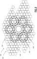
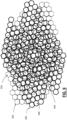
- FIG. 8 shows the ⁇ LEDs projected spots onto the multi-core fiber cable 840 displayed as a fiber bundle 802 (shown as a honeycomb array).
- the hexagonal honeycomb array represents individual fibers 830.
- a plurality of ⁇ LED illumination zones 844 and ⁇ LED exclusion zones 846 are shown.
- the ⁇ LED exclusion zones 846 shown in the present embodiment are at least 2 fibers 830 wide, and the ⁇ LED illumination zones 844 are 1 or 2 fibers 830 wide (2 fibers wide in the present example).
- the fiber bundle 802 makes up a fiber cable 840 and is assumed as a fixed reference point where the ⁇ LED portion of a chip 100 can have any X axis, Y axis, and angular misalignment.
- embodiments may include ⁇ LED illumination zones 844 and ⁇ LED exclusion zones 846 of any size, shape, and orientation. Additionally, other embodiments may include fiber cores 830 of different size and shape as well as larger or smaller cladding 848.
- the embodiment shown in FIG. 8 shall be construed as a non-limiting example.
- FIG. 9 is a diagram illustrating a PD array 950 with misalignment to the fiber cores 930 of FIG. 8 .
- the figure shows a honeycomb representing individual PDs 906 overlayed onto the fiber cores 930 and illumination zones 944 of FIG. 8 to simulate a connection of a fiber cable to a chip housing the PD array 950.
- Groupings of 4 PDs 906 can collect from most fiber cores 930 with significant light, though still some loss is observed due to uncollected light.
- a grouping of 7 PDs 906 to form a flower like pattern collects nearly all of the light but requires more complex circuitry. Changing ⁇ LED illumination to 1 core improves the 4 PD collection efficiency.
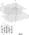
- FIG. 10 is a diagram of an example of a fuse-based implementation with 4-PD groups.
- each PD has potential connections to 4 TIAs and each PD is allowed to connect to 1 TIA, with other connections broken represented by the broken connections 1056.
- all PD connections are initially preserved, 1 ⁇ LED is enabled in Continuous Wave (CW) mode, and the TIA with the largest CW signal is determined.
- CW Continuous Wave
- FIG. 10 A magnified image is also provided in FIG. 10 to better show the preserved and broken connections.
- the preserved connections 1058 can be seen traveling from the TIA 1054 to the 4 surrounding PDs 1052. Also more clearly seen are the broken connections 1056 from the 4 PDs to the other surrounding TIAs.
- the disclosed alignment circuitry connected to the ⁇ LEDs and the PDs can further be configured to select a set of fiber cores.
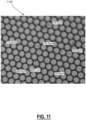
- FIG. 11 is a magnified image of a cluster of fiber cores 1130 showing the slight variation in size.
- the total diameter of the bundle of fiber cores shown in FIG. 11 is 0.35mm with a total of 3,500 fiber cores 1130.
- the individual fiber core 1130 diameter is 5 micrometers with a cladding 1148 thickness of 1 micrometer. From the figure, the fiber cores 1130 range from a diameter of 4.5 - 4.8 micrometers while the cladding ranges from 0.8 - 0.9 micrometers. Therefore, ⁇ LED spots will have different alignments with fiber cores.
- FIG. 12 is a diagram of a side view of a plurality of ⁇ LEDs 1208 and PDs 1206 aligned with a bundle 1202 of fiber cores 1230.
- the diagram displays TX and RX sides of a connection, the connection being made by the fiber bundle 1202.
- the connection via the fiber bundle 1202 transmits light from the plurality of LEDs 1208 to the plurality of PDs 1206.
- An example side-view of 3 illumination alignments (1266a, 1266b, 1266c) is shown in FIG. 12 which shows how spot size (illumination zone) 1244 at the PDs 1206 can vary depending on alignment.
- Selectively disabled PDs 1206 are also shown in FIG. 12 . It shows how the number of PDs 1206 used in a channel can depend on natural alignment and variation of the fiber cores 1230.
- a first PD alignment 1260a of PDs 1206 is shown as an example alignment with only 1 disabled PD 1262.
- a second alignment 1260b of PDs 1206 shows a plurality of disabled PDs 1262, wherein disabled PDs 1262 are selected based on location and light absorption from the ⁇ LEDs 1208.
- the ⁇ LEDs 1208 transmit light through a plurality of lenses 1232 and create spots 1264 with a separation equal to approximately 2 fiber cores 1230.
- the fiber bundle 1202 includes cladding 1248 which creates loss between the fiber cores 1230. The light travels through the fiber cores 1230 and exits onto the PDs 1206 creating RX spots (illumination zones) 1244.
- Additional loss is encountered between the PDs 1206 with disabled PDs 1262 being selected based on where the light is not present.
- Overlapping illumination zones 1244 occur when two adjacent fiber cores 1230 emit light onto the PDs 1206 causing some light to overlap.
- a front view is shown which depicts a 9 core distribution and a 16 core distribution.
- the 9 core distribution includes an ⁇ LED 1208 at every 3rd fiber core 1230, while the 16 core distribution includes an ⁇ LED 1208 at every 4th fiber core 1230.
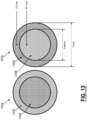
- FIG. 13 is a diagram of ⁇ LEDs 1308 and PDs 1306 distributed on a chip 100 including alternative segmentation of TX ( ⁇ LED) and RX (PD) areas.
- alternative segmentation of Transmit (TX) and Receive (RX) areas are contemplated where each area corresponds to about half of the area of the chip.
- An alternate annular mode is described herein which includes the advantage of being resistant to angular misalignment assuming satisfactory X and Y axis alignment.
- the figure includes a first chip 100a and a second chip 100b where the first chip 100a includes the ⁇ LEDs 1308 along an inner area and the PDs 1306 along an outer ring, whereas the second chip 100b includes the ⁇ LED 1308 along the outer ring and the PDs 1306 along the inner area.
- the first chip 100a and second chip 100b demonstrate two sides of a connection, where the ⁇ LEDs 1308 from the first chip will transmit light through fiber cores of a fiber cable onto the PDs 1306 of the second chip 100b, and the ⁇ LEDs 1308 of the second chip 100b will transmit to the PDs 1306 of the first chip 100a.
- TX and RX areas are contemplated.
- a chip can include any number of TX ( ⁇ LED) areas and any number of RX (PD) areas.
- PD RX
- any combination of TX and RX areas are also contemplated herein, for example a different number of TX areas than RX areas.
- the embodiments disclosed herein showing one TX area and one RX area shall be construed as a non-limiting example.
- the present disclosure provides various features for increasing tolerance to misalignment of optical transceivers described herein.
- the annular partitioning of ⁇ LED and PD arrangements described herein allows for angular insensitivity of fiber alignment.
- additional ⁇ LED and PD devices can be strategically located near split lines (i.e., the border between ⁇ LEDs and PDs) to allow for additional coarse misalignment tolerances.
- Various embodiments include utilizing dark (unilluminated) fiber core guard bands between ⁇ LED devices to increase tolerance to misalignment between ⁇ LEDs, imaging fiber (fiber cores), and PDs.
- Various embodiments include minimizing dark areas between PDs to increase light collection efficiency. The ability to selectively combine signals from multiple PDs greatly improves SNR and thereby link budget.
- Selection of specific PD groupings is implemented either at manufacturing and fixed, or during operation. If selection of specific PD groupings is done during operation, it should facilitate extensions to connectorized fibers and or external fiber patch cord use with possible angular and Cartesian (X,Y) misalignment.
- a specific efficient procedure for determining the particular grouping of PDs into a single data channel output is also utilized by various embodiments of the present disclosure.
- PD membership in a grouping may be dependent on a limiting parameter. For example, post-TIA summation is limited by TIA noise and its impact on SNR. Direct PD photocurrent summation is limited by PD capacitance and impact on bandwidth. Further, various embodiments include an additional guard band on areas of devices (optical transceivers) that may be either more expensive or more prone to failure.
- Table 1 below provides a context of the interconnect cabling market. The present disclosure focuses on a module and technique to address 10m and less to avoid the cost burden of longer reaches (e.g., 300m). Of note, the inventors submit there is a need for high-bandwidth interconnects at 10m and less. Table 1 Addressable Volume Max Reach Racks System BW 'Hundred thousands' 300m Multi-rack same room (blast radius) >96Tb/s 'Millions' 10m Adjacent 3-rack 192Tb/s 'Billions' 1cm - 2m Single-rack 96Tb/s
- Table 2 below provides a context of the existing approaches and costs relative to the present disclosure. This example assumes a 400Gb/s interconnect, but the present disclosure also contemplates 800Gb/s and higher including 1Tb/s and beyond. Table 2 400G cable Cost Comments 2m DAC $X Twinax power increasing, reach decreasing, install issues. 10m Present disclosure $2X Low cost: ⁇ LED array, non-precision alignment, integrated micro-optics, low baud rate MIMO, MMF, standard form factor. 7m AEC $5X Install issues, reach issues, copper BW limits. 10m Open-eye AOC $6X Marginally cheaper due to simpler equalization 10m VCSEL AOC $8X high power and complexity CPO $8X high power and complexity
- FIG. 14 is a diagram of an optical link 10 showing the VCSEL array 12a, 12b on both ends of MMF fiber 14 along with a transmitter circuit 16 and a receiver circuit 18.
- FIG. 15 is a diagram of the optical link 10 illustrating orthogonal speckles on the MMF fiber 14.
- FIG. 16 is a diagram of the optical link 10 illustrating bend sensitivity on the MMF fiber 14.
- FIG. 17 is a diagram of the optical link 10 illustrating ultra-coarse Wavelength Division Multiplexing (WDM) on the VCSEL array 12a.
- WDM Wavelength Division Multiplexing
- the optical link 10 is shown in a unidirectional configuration.
- the VCSEL arrays 12a, the PD arrays12b, the transmitter circuit 16, and the receiver circuit 18 can be integrated in a single form factor, such as a module, circuit, etc.
- the transmitter circuit 16 includes a transmit Multi-Input Multi-Output (MIMO) Digital Signal Processor (DSP) connected to a Digital-to-Analog Converter (DAC) that connects to the VCSEL array 12a.
- MIMO Multi-Input Multi-Output
- DSP Digital Signal Processor
- DAC Digital-to-Analog Converter
- the VCSEL array 12a is a 14x14 array with 196 total pixels, supporting 10Gb/s per pixel. With 100 active pixels, this supports 1Tb/s and has a size of about 140 ⁇ m ⁇ 140 ⁇ m.
- the MMF fiber 14 can be a 125 ⁇ m graded-index MMF (GRIN MMF) of about 10m. 62.5 ⁇ m MMF support 220 SDM channels. A larger 125 ⁇ m MMF increases speckle dots, which makes classification easier and allows larger VCSELs. Dispersion is not an issue at 10 meters and low baud.
- the VCSEL array 12a is configured to drive the GRIN MMF fiber 14. The VCSEL array 12a is larger than the MMF input facet.
- the VCSEL array 12a can be a RGB VCSEL array whereby different-color VCSELs are placed closer together.
- the VCSEL array 12b is a sensor without a RGB passive color filter. This because speckle patterns are orthogonal with sufficiently different wavelengths.
- the VCSEL arrays 12a, 12b can be on-die, integrated devices.
- a training algorithm determines which VCSELs are able to couple light into the MMF fiber 14 and which are not. This avoids precise manufacturing alignment requirements.
- a continuous training algorithm detects dynamic physical perturbation (e.g., bending, temperature, vibration) in the MMF fiber 14 and recalibrates a Transmission Matrix. This can also be used to detect physical tampering for high-security systems, detect seismic activity, detect cable movement by installer, etc.
- the MMF fiber 14 connects to the VCSEL array 12b which can include a 20x20 sensor array with 400 pixels.
- the receiver circuit 18 includes a gain and Analog-to-Digital Converter (ADC) and a receiver DSP.
- ADC Analog-to-Digital Converter
- the present disclosure includes a low symbol rate that avoids Intersymbol interference (ISI) issues due to modal dispersion and chromatic dispersion at ⁇ 10m distances. This applies even at blue wavelengths of ⁇ 500nm.
- ISI Intersymbol interference
- the optical link 10 can be constructed with current, consumer technology, i.e., the VCSEL arrays 12a, 12b with integrated lens, sensor array.
- the present disclosure exploits various Orthogonal dimensions: Amplitude / Phase / Frequency / Color / Space to obtain high-capacity at low-cost.
- MMF 14 large-diameter (1000 ⁇ m) multimode GRIN POF (Plastic Optical Fiber) such as OM-GIGA.
- MMF 14 large-diameter (1000 ⁇ m) multimode GRIN POF (Plastic Optical Fiber) such as OM-GIGA.
- the present disclosure also contemplated single-fiber bidirectional operation without a beam splitter by having ⁇ LED's and sensors integrated on the same array.
- the present disclosure can include multiple FMF (Few Mode Fiber) fan-out cables (optical-to-optical repeater demux).
- FMF Frew Mode Fiber
- fan-out cables optical-to-optical repeater demux
- FIG. 18 is a diagram of a training and Forward Error Correction (FEC) process for the VCSEL arrays 12a, 12b.
- FEC Forward Error Correction
- MGDM Mode Group Diversity Multiplexing
- the correlation-based classifier has to separate non-zero cross-correlations as low as 1/sqrt( N ) from zero-mean cross-correlations. This becomes harder for larger N .
- a partial solution would be to reduce the statistical noise which distorts these correlation coefficients. This can be achieved by increasing the number of speckle spots (currently -300-300), e.g., by using an MMF with a larger core.
- the classification results obtained with the linear classifiers suggest that the number of speckle intensity samples should only exceed the number of SDM channels by a small margin in order to obtain robust operation. Therefore, also the number of speckle spots across the fiber end facet only needs to exceed the number of SDM channels by a small margin.
- the patterns generated by multiple beams have a lower speckle contrast than the patterns generated by any single beam, of which the speckle contrast C 1 is approximately 1/sqrt(2) due to polarization diversity.
- the speckle contrast is reduced to C 1 / sqrt(n).
- a lower speckle contrast is expected to make the pattern classification task more difficult, as in this context the speckle contrast can be viewed as a signal-to-noise ratio.
- Detectors in such an array only need to sample the local speckle intensities (rather than full-view imaging).
- GRIN fiber reduces modal dispersion.
- the longer-length paths spend most of their time in lower refractive index material where the velocity is faster.
- the shortest path is the axial path which spends all its time in the higher-refractive index material and has the slowest velocity.
- a GRIN MMF with a realistically imperfect profile probably has a pulse broadening of about 500 ps/km. So, the pulse broadening for a 2m fiber would be 1 ps across all modes. That is a minimal guard band to insert into a 500 ps symbol period. And realistically the pulse-broadening is 100X smaller since we're exciting a subset of modes as discussed above.
- Table 3 illustrates Architecture choices and trade-offs Table 3 Architecture trade-offs Cost Power Comments Copper Twinax / Fiber - ⁇ Fiber has long runway, lower power at higher rates, lower space/weight, better installability. Copper becoming increasingly impractical (power/bit, 224G Xtalk, etc). 2m / 10m / 100m / 300m ⁇ ⁇ Low-cost: Focus on ultra-short reach, which reduces complexity due to Modal/Chromatic dispersion and loss. Polarization / OFDM QAM (Amplitude & Phase of sub-carriers) / WDM / SDM ⁇ SDM is a large multiplier. SISO / MIMO ⁇ - Per pixel data rate can equal or be close to lowest possible power CMOS interface rate.
- Pluggable / CPO RLS - - -- OSFP-XD/QSFP-DD form factor allow full range of reach (2m to hundreds of km). -- CPO still uses lots of faceplate and never going to go hundreds of km. Shared lasers not necessarily a good redundancy model. Chiplet interconnect Match optical baud rate to electrical baud rate to avoid gear box. 10-20Gbps electrical today.
- imaging This can include "-oscopy” such as Medical Endoscopy, Industrial Boroscopy (sewers, machinery, structures, engine blocks), Microscopy, and the like. Also, this can be used for integrating a sensor and a display for an in-screen fingerprint sensor. Even further this can be used in automotive - cars have numerous cameras and this will increase. Fiber bundles enable camera arrays in compact spaces: 3D imaging.
- embodiments provide a novel implementation using ⁇ LED based optical links in combination with electronic crosspoint switches. This simultaneously achieves low latency, low cost, low power, and high bandwidth.
- the invention includes ⁇ LED & PD (Photodetector) IO and an electronic crosspoint switch all on a single chip (or vertical 3D stack of chips) (refer to FIG. 1 - FIG. 13 ).
- the ⁇ LED based optical links provide a low cost and low power optical interconnect while sacrificing optical reach to ⁇ 10 meters.
- the present disclosure describes a specific embodiment for simplicity, but it will be appreciated that other arrangements are contemplated in other embodiments.
- FIG. 20 is a diagram of imaging fiber bundles 2302 linked to the optical switch system 2300 of the present disclosure.
- Fiber bundles 2302 combine hundreds or thousands of individual transmission fiber cores with thin cladding between each core and with preserved physical position of cores between input and output facets.
- the imaging fiber bundles 2302 of the present embodiment each contain about 4000 cores and pass 1.6Tb of data, with a typical channel rate below 10 Gbps (several fiber cores 'image' one source to a receiver).
- the imaging fiber is ⁇ 1mm in diameter and an entire chip can handle 1250 such bundles, which is 2000 Tb total IO capacity.
- the fiber bundles 2302 are all de-jacketed and grouped together to land on the photodetector (PD) array 2304 on the faceplate 2308 of the chip.
- the diagram shows square arrays, but these arrays can be circular or other shapes known to one of skill in the art. Also shown are separate PD arrays 2304 and ⁇ LED arrays 2306, but these can be intermingled in various shapes as well (refer to previous sections of this disclosure).
- each fiber bundle 2302 has 402 channels carried on 4000 individual fiber cores. Each channel may operate at 4Gbps NRZ with 1 clock-only channel, 1 address channel, and 400 data-only channels.
- the PD arrays 2304 of the present embodiment can support 1250 1mm sub-arrays where a given sub-array maps to a single fiber bundle 2302.
- the ⁇ LED arrays 2306 can similarly support 1250 1mm sub-arrays.
- An electronic crosspoint switch 2310 allows the optical switching system 2300 to switch at the fiber bundle level and additionally be buffer-less, while flip flops 2312 re-time each wire. It will be appreciated that the embodiment shown in FIG. 20 is a non-limiting example, and the number of fiber cores, fiber bundles, PD arrays, and ⁇ LED arrays can be different in other embodiments.
- FIG. 21 is a diagram of the non-blocking crosspoint switch of the present disclosure.
- the crosspoint switch 2410 includes a plurality of ports 2414 where each port includes a plurality of signals.
- a port 2414 may be several data channels synchronously grouped together to transmit a standards-compliant higher data rate signal (i.e., 100Gb Ethernet, OTU4, ODUFlex, 400Gb Ethernet, etc.).
- the crosspoint switch includes 398x398 ports, each including 400 signals resulting in 64M intersections. Each intersection includes 2 transmission gate transistors resulting in a total of 128M transmission gate transistors.
- Each ⁇ LED IO (including driver) takes about 36x36um of space and 400 ⁇ LEDs are used per bundle.
- each input port and each output port can include a plurality of signals forming an aggregate signal.
- ⁇ LED drivers and PD TIAs are on the same substrate as the crosspoint switch ASIC.
- the clock signal is transmitted on a separate ⁇ LED link and associated with several data channels forming a single port, which makes clock recovery much more simple and lower power. There may be 1 or more ports associated with a single fiber bundle.
- Combining clock and data channels with crosspoint switches is contemplated, such that somewhat randomized association of received data and clock is compensated by the crosspoint, and correct input and output mapping is restored with proper clocking to provide full 3R signal regeneration (Reamplify, Reshape, Retime).
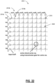
- FIG. 22 is a diagram of an 8x8 crosspoint switch.
- the crosspoint switch 2510 is connected to 8 input ports 2514a and 8 output ports 2514b.
- the electrical crosspoint switch 2510 additionally includes a plurality of input traces 2518a connected to each input port 2514a and a plurality of output traces 2518b connected to each output port 2514b.
- the input ports 2514a and 8 output ports 2514b are adapted to couple to a plurality of fiber bundles (i.e., input fiber bundles and output fiber bundles).
- the plurality of input ports 2514a and output ports 2514b can be connected via the plurality of intersections 2515 by a plurality of switches 2520.
- the crosspoint switch 2510 of the present disclosure includes input traces 2518a and output traces 2518b in a vertical and horizontal orientation relative to each other.
- each input port 2514a is a photodiode array and each output port 2514b is a micro light emitting diode array. It will be appreciated that other arrangements and numbers of input and output lines and ports are contemplated.
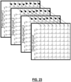
- FIG. 23 is a diagram of a layered electronic crosspoint switch approach of the present disclosure.
- the present disclosure provides a layered crosspoint approach to simplify control and reduce individual crosspoint size.
- a fiber bundle has 8 distinct ports 2514.
- Each port 2514 can be switched to an arbitrary output (i.e., 8 input ⁇ 8 output).
- the data channels and clock forming a port are all switched synchronously to the same port output.
- the clock is used to retime corresponding data channel output.
- the plurality of input ports 2514a, the plurality of output ports 2514b, and the electrical crosspoint switch 2510 are copackaged together.
- the present disclosure provides 32x32 crosspoints for 10Gbps signals, which can be modeled as lumped elements.
- Switch cells are approximately 10x10 micron in 45 nm 12SOI CMOS. Assuming a 32x32 switch, total signal propagation distance between IO buffers is 640 microns.
- CMOS transmission line in crosspoint has a velocity of 1.7e8 m/s, which corresponds to a 640e-6/1.7e8 ⁇ 4 ps total propagation delay across the crosspoint in a worst case (excluding buffers).
- 10 Gbps signals have 100 ps bit period, so 4 ps is not significant and a 32 ⁇ 32 crosspoint can be considered as a lumped element.
- a large switching fabric can be constructed from smaller, individually buffered, and clocked units.
- a 32x32 crossspoint will occupy ⁇ 320x320 um2.
- Total number of unit switches is 19008 units. Assuming each unit switch consumes 20 mW of buffer power, total power is ⁇ 400 W. Optical links are expected to consume 1W/1Tbps. Composite 640Tbps switch optical IO will therefor consume 640 W. Total power consumption is ⁇ 1000W for a 640 Tbps switch with optical IO, which is ⁇ 2 pJ/bit. For comparison, typical 400G-DR4 pluggable modules are ⁇ 18 pJ/bit, and low-power CoPackaged Optical (CPO) is pursuing initial designs with ⁇ 14 pJ/bit, both without providing any switching functionality.
- CPO CoPackaged Optical
- Each unit switch would occupy 800 ⁇ 800 um2.
- Switch size is same as before ⁇ 66 mm ⁇ 30 mm with each switch at 50 mW, total power is reduced considerably to ⁇ 132 W.
- the present optical switch system can be controlled by an external controller.
- a method is also proposed that uses a dedicated ⁇ LED for addressing, which enables a source-routed switch. Multiple inputs to switch to a single output is blocked by the present embodiment, however, some amount of multi-casting (single input to multiple outputs) is possible with crosspoint designs contemplated in various embodiments.
- Media conversion with the present optical switch system is achieved by plug personality. For example, converting from short-reach 10-meter ⁇ LED link to a 400km coherent line.
- FIG. 24 is a diagram of media conversion via plugs with the optical switch system of the present disclosure.
- a serialization mode is used.
- the optical switch system operates on Bunch of Wires (BoW) groups (not individual wires), which are slow and highly parallel buses used to communicate inside chips. By operating at these slow speeds, it allows for very large crosspoint matrices since the resulting stubs don't present signal integrity issues at the slow 4Gbps speeds. It will be appreciated that other embodiments include other modes (e.g. serialization step ahead of the crosspoint).
- embodiments utilize a switching granularity mode.
- One extreme is crosspoint switching per ⁇ LED channel.
- the other extreme is the system described in the present disclosure (i.e., switching granularity is at the fiber/port level).
- sub-group switching granularity is also contemplated. The more granularity, the more control electronics are required within the crosspoint switch.
- lasers are utilized instead of ⁇ LEDs, and packet-based switching can be used through the addition of more address bits to the dedicated ⁇ LED address signal.
- embodiments can utilize a timeslot guard band clock cycle.
- the plurality of input ports and the plurality of output ports are short reach devices, and further including one or more long reach optical modems connected to one or more of the output ports.
- the short reach devices can be ten meter modems, and the one or more long reach optical modems can be coherent modems.
- a full 3D monolithic integration of the crosspoint switch of the present disclosure is also contemplated, which allows a vertical interconnect that is very short and thus low-capacitance relative to existing 2D tiled structures.
- a 3D stackup of the ⁇ LED switch is represented.
- the 3D stackup allows ⁇ LED arrays 100a to be positioned atop the crosspoint array 634.
- the plurality of input ports are in a micro light emitting diode array circuit
- the plurality of output ports are in a photodiode array circuit
- the electrical crosspoint switch is in a switch circuit
- the micro light emitting diode array circuit and the photodiode array circuit are stacked on the switch circuit. This reduces overall power and increases switch scale.
- the regular structure of a crosspoint switch lends itself to 3D integration; building tiles of a certain size via manual layout and then replicating those tiles in X, Y and Z directions to achieve the most area efficient crosspoint switch.
- the optical switch system of the present disclosure provides a combination of ⁇ LED arrays, PDs, imaging fiber bundles, and crosspoint switch on a single chip.
- a 3D stackup of ⁇ LED, PD, and crosspoint array dies results in substantial density and bandwidth increase along with a concentration of multiple imaging fiber bundles on a single chip using an optical taper.
- Embodiments provide dedicated ⁇ LEDs for clock and address, with Clocking and Address shared across several ⁇ LED data channels that form a port. Additionally, BoW switching is utilized as opposed to switching serialized signals, and IO is accessible from the surface of the switch rather than its edges.
- processors such as microprocessors; Central Processing Units (CPUs); Digital Signal Processors (DSPs): customized processors such as Network Processors (NPs) or Network Processing Units (NPUs), Graphics Processing Units (GPUs), or the like; Field-Programmable Gate Arrays (FPGAs); and the like along with unique stored program instructions (including both software and firmware) for control thereof to implement, in conjunction with certain non-processor circuits, some, most, or all of the functions of the methods and/or systems described herein.
- processors such as microprocessors; Central Processing Units (CPUs); Digital Signal Processors (DSPs): customized processors such as Network Processors (NPs) or Network Processing Units (NPUs), Graphics Processing Units (GPUs), or the like; Field-Programmable Gate Arrays (FPGAs); and the like along with unique stored program instructions (including both software and firmware) for control thereof to implement, in conjunction with certain non-processor circuits, some, most, or all
- circuitry configured to
- logic configured to
- some embodiments may include a non-transitory computer-readable medium having instructions stored thereon for programming a computer, server, appliance, device, at least one processor, circuit/circuitry, etc. to perform functions as described and claimed herein.
- Examples of such non-transitory computer-readable medium include, but are not limited to, a hard disk, an optical storage device, a magnetic storage device, a Read-Only Memory (ROM), a Programmable ROM (PROM), an Erasable PROM (EPROM), an Electrically EPROM (EEPROM), Flash memory, and the like.
- software can include instructions executable by one or more processors (e.g., any type of programmable circuitry or logic) that, in response to such execution, cause the one or more processors to perform a set of operations, steps, methods, processes, algorithms, functions, techniques, etc. as described herein for the various embodiments.
- processors e.g., any type of programmable circuitry or logic
Landscapes
- Physics & Mathematics (AREA)
- General Physics & Mathematics (AREA)
- Optics & Photonics (AREA)
- Engineering & Computer Science (AREA)
- Computer Networks & Wireless Communication (AREA)
- Signal Processing (AREA)
- Electromagnetism (AREA)
- Optical Couplings Of Light Guides (AREA)
- Optical Communication System (AREA)
- Use Of Switch Circuits For Exchanges And Methods Of Control Of Multiplex Exchanges (AREA)
- Mechanical Light Control Or Optical Switches (AREA)
Applications Claiming Priority (3)
| Application Number | Priority Date | Filing Date | Title |
|---|---|---|---|
| US202163238419P | 2021-08-30 | 2021-08-30 | |
| PCT/US2022/042034 WO2023034298A1 (en) | 2021-08-30 | 2022-08-30 | Micro-led/pd arrangements and selection in an optical interconnect over fiber cable having multiple fiber cores |
| EP22777437.9A EP4173174B1 (de) | 2021-08-30 | 2022-08-30 | Mikro-led/pd-anordnungen und auswahl in einer optischen verbindung über ein faserkabel mit mehreren faserkernen |
Related Parent Applications (2)
| Application Number | Title | Priority Date | Filing Date |
|---|---|---|---|
| EP22777437.9A Division EP4173174B1 (de) | 2021-08-30 | 2022-08-30 | Mikro-led/pd-anordnungen und auswahl in einer optischen verbindung über ein faserkabel mit mehreren faserkernen |
| EP22777437.9A Division-Into EP4173174B1 (de) | 2021-08-30 | 2022-08-30 | Mikro-led/pd-anordnungen und auswahl in einer optischen verbindung über ein faserkabel mit mehreren faserkernen |
Publications (2)
| Publication Number | Publication Date |
|---|---|
| EP4436075A2 true EP4436075A2 (de) | 2024-09-25 |
| EP4436075A3 EP4436075A3 (de) | 2024-12-11 |
Family
ID=83447879
Family Applications (2)
| Application Number | Title | Priority Date | Filing Date |
|---|---|---|---|
| EP22777437.9A Active EP4173174B1 (de) | 2021-08-30 | 2022-08-30 | Mikro-led/pd-anordnungen und auswahl in einer optischen verbindung über ein faserkabel mit mehreren faserkernen |
| EP24193949.5A Pending EP4436075A3 (de) | 2021-08-30 | 2022-08-30 | Kreuzpunktschalter mit ¢led-io-ports und abbildungsfaserkabeln |
Family Applications Before (1)
| Application Number | Title | Priority Date | Filing Date |
|---|---|---|---|
| EP22777437.9A Active EP4173174B1 (de) | 2021-08-30 | 2022-08-30 | Mikro-led/pd-anordnungen und auswahl in einer optischen verbindung über ein faserkabel mit mehreren faserkernen |
Country Status (5)
| Country | Link |
|---|---|
| US (2) | US12348913B2 (de) |
| EP (2) | EP4173174B1 (de) |
| CN (2) | CN117242716B (de) |
| CA (1) | CA3211841A1 (de) |
| WO (1) | WO2023034298A1 (de) |
Families Citing this family (3)
| Publication number | Priority date | Publication date | Assignee | Title |
|---|---|---|---|---|
| US20230034270A1 (en) * | 2021-07-28 | 2023-02-02 | Apple Inc. | Optical Fiber Illumination by a Set of Light Emitters |
| US12332488B2 (en) * | 2021-08-17 | 2025-06-17 | Avicenatech, Corp. | MicroLED parallel optical interconnects |
| EP4483510A4 (de) * | 2022-02-23 | 2025-06-11 | Avicenatech, Corp. | Parallele optische freiraumverbindungen auf mikro-led-basis |
Family Cites Families (12)
| Publication number | Priority date | Publication date | Assignee | Title |
|---|---|---|---|---|
| US4114112A (en) * | 1976-12-22 | 1978-09-12 | Northwestern University | Apparatus and method for efficient synthesis of laser light |
| JP3582030B2 (ja) * | 1995-07-05 | 2004-10-27 | 富士通株式会社 | クロスコネクト装置 |
| CN101742363A (zh) * | 2008-11-20 | 2010-06-16 | 华为技术有限公司 | 一种光交换的方法和装置 |
| US9756404B2 (en) * | 2014-07-03 | 2017-09-05 | Fiber Mountain, Inc. | Data center path switch with improved path interconnection architecture |
| US9648402B2 (en) * | 2015-02-10 | 2017-05-09 | Ciena Corporation | In-band communication channel in optical networks |
| WO2017028873A1 (en) * | 2015-08-14 | 2017-02-23 | Telefonaktiebolaget Lm Ericsson (Publ) | Interconnection network and method of routing optical signals |
| EP3391108A1 (de) * | 2015-12-17 | 2018-10-24 | Universite d'Aix-Marseille (AMU) | Systeme und verfahren für hochauflösende bildgebung anhand eines glasfaserbündels |
| JP6707932B2 (ja) * | 2016-03-22 | 2020-06-10 | 富士ゼロックス株式会社 | 情報処理装置 |
| GB201620744D0 (en) * | 2016-12-06 | 2017-01-18 | Roadmap Systems Ltd | Multimode fibre optical switching systems |
| US12167184B2 (en) * | 2018-04-02 | 2024-12-10 | Rensselaer Polytechnic Institute | Cross-connect switch architecture |
| US11624882B2 (en) * | 2019-09-13 | 2023-04-11 | Avicenatech Corp. | Optical interconnects using microLEDs |
| US11153670B1 (en) * | 2020-04-14 | 2021-10-19 | Nubis Communications, Inc. | Communication system employing optical frame templates |
-
2022
- 2022-08-30 CN CN202280029089.7A patent/CN117242716B/zh active Active
- 2022-08-30 CN CN202510321490.3A patent/CN119995726A/zh active Pending
- 2022-08-30 CA CA3211841A patent/CA3211841A1/en active Pending
- 2022-08-30 EP EP22777437.9A patent/EP4173174B1/de active Active
- 2022-08-30 WO PCT/US2022/042034 patent/WO2023034298A1/en not_active Ceased
- 2022-08-30 EP EP24193949.5A patent/EP4436075A3/de active Pending
-
2023
- 2023-01-20 US US18/099,473 patent/US12348913B2/en active Active
-
2024
- 2024-08-08 US US18/797,868 patent/US20250048006A1/en active Pending
Also Published As
| Publication number | Publication date |
|---|---|
| WO2023034298A1 (en) | 2023-03-09 |
| CN117242716B (zh) | 2025-04-04 |
| EP4173174A1 (de) | 2023-05-03 |
| EP4436075A3 (de) | 2024-12-11 |
| CA3211841A1 (en) | 2023-03-09 |
| US12348913B2 (en) | 2025-07-01 |
| CN117242716A (zh) | 2023-12-15 |
| US20230232138A1 (en) | 2023-07-20 |
| US20250048006A1 (en) | 2025-02-06 |
| EP4173174B1 (de) | 2024-10-23 |
| CN119995726A (zh) | 2025-05-13 |
Similar Documents
| Publication | Publication Date | Title |
|---|---|---|
| EP4173174B1 (de) | Mikro-led/pd-anordnungen und auswahl in einer optischen verbindung über ein faserkabel mit mehreren faserkernen | |
| CN113853753B (zh) | 光子通信平台 | |
| EP3063574B1 (de) | Gemultiplexte optoelektronische engines | |
| US9354412B2 (en) | Optical interconnect fabrics and optical switches | |
| Dorren et al. | Challenges for optically enabled high-radix switches for data center networks | |
| US9097874B2 (en) | Polarity configurations for parallel optics data transmission, and related apparatuses, components, systems, and methods | |
| TWI546579B (zh) | 光學架構、光學分配矩陣及製造光學結構之方法 | |
| CN106353859A (zh) | 一种光互联交叉背板、传输设备及信号调度方法 | |
| Pezeshki et al. | 304 channel MicroLED based CMOS transceiver IC with aggregate 1 Tbps and sub-pJ per bit capability | |
| US10063337B1 (en) | Arrayed waveguide grating based multi-core and multi-wavelength short-range interconnection network | |
| CN112804002A (zh) | 基于mpo光纤跳线的短距互连网络 | |
| US7639903B2 (en) | Daisy chain optical interconnect | |
| US12392958B2 (en) | Imaging lantern for enhanced optical transmission | |
| Kurata et al. | Prospect of chip scale silicon photonics transceiver for high density multi-mode wiring system | |
| CN114859482A (zh) | 一种用于硅光芯片的光路系统 | |
| CN219738151U (zh) | 片上模分复用/解复用器 | |
| CN207764432U (zh) | 光学装置和光模块 | |
| CN121261790A (zh) | 一种高带宽密度光互联结构与光通信系统 | |
| CN119728599A (zh) | 片上全光交换网络设备、半导体装置及其制造方法 | |
| JPWO2014049852A1 (ja) | 光ファイバと接続する光路変換光結合デバイスおよび光モジュール | |
| Yamada et al. | Optical Bus Technology | |
| EP3175274A1 (de) | Polaritätskonfigurationen für parallele optische datenübertragung und entsprechende vorrichtungen, komponenten, systeme und verfahren | |
| Tatum | VCSELs in optical networking |
Legal Events
| Date | Code | Title | Description |
|---|---|---|---|
| PUAI | Public reference made under article 153(3) epc to a published international application that has entered the european phase |
Free format text: ORIGINAL CODE: 0009012 |
|
| STAA | Information on the status of an ep patent application or granted ep patent |
Free format text: STATUS: THE APPLICATION HAS BEEN PUBLISHED |
|
| AC | Divisional application: reference to earlier application |
Ref document number: 4173174 Country of ref document: EP Kind code of ref document: P |
|
| AK | Designated contracting states |
Kind code of ref document: A2 Designated state(s): AL AT BE BG CH CY CZ DE DK EE ES FI FR GB GR HR HU IE IS IT LI LT LU LV MC MK MT NL NO PL PT RO RS SE SI SK SM TR |
|
| REG | Reference to a national code |
Ref country code: DE Ref legal event code: R079 Free format text: PREVIOUS MAIN CLASS: H04J0014040000 Ipc: H04B0010258100 |
|
| PUAL | Search report despatched |
Free format text: ORIGINAL CODE: 0009013 |
|
| AK | Designated contracting states |
Kind code of ref document: A3 Designated state(s): AL AT BE BG CH CY CZ DE DK EE ES FI FR GB GR HR HU IE IS IT LI LT LU LV MC MK MT NL NO PL PT RO RS SE SI SK SM TR |
|
| RIC1 | Information provided on ipc code assigned before grant |
Ipc: G02B 6/43 20060101ALI20241105BHEP Ipc: G02B 6/02 20060101ALI20241105BHEP Ipc: H04J 14/00 20060101ALI20241105BHEP Ipc: H04Q 11/00 20060101ALI20241105BHEP Ipc: G02B 6/42 20060101ALI20241105BHEP Ipc: H04J 14/04 20060101ALI20241105BHEP Ipc: H04B 10/2581 20130101AFI20241105BHEP |
|
| P01 | Opt-out of the competence of the unified patent court (upc) registered |
Free format text: CASE NUMBER: APP_61410/2024 Effective date: 20241115 |
|
| STAA | Information on the status of an ep patent application or granted ep patent |
Free format text: STATUS: REQUEST FOR EXAMINATION WAS MADE |
|
| 17P | Request for examination filed |
Effective date: 20250602 |