EP4434762A1 - Optisch variables element, sicherheitsdokument, verfahren zur herstellung eines optisch variablen elements, verfahren zur herstellung eines sicherheitsdokuments - Google Patents
Optisch variables element, sicherheitsdokument, verfahren zur herstellung eines optisch variablen elements, verfahren zur herstellung eines sicherheitsdokuments Download PDFInfo
- Publication number
- EP4434762A1 EP4434762A1 EP24173126.4A EP24173126A EP4434762A1 EP 4434762 A1 EP4434762 A1 EP 4434762A1 EP 24173126 A EP24173126 A EP 24173126A EP 4434762 A1 EP4434762 A1 EP 4434762A1
- Authority
- EP
- European Patent Office
- Prior art keywords
- structures
- pixels
- optically variable
- pixel array
- pixel
- Prior art date
- Legal status (The legal status is an assumption and is not a legal conclusion. Google has not performed a legal analysis and makes no representation as to the accuracy of the status listed.)
- Pending
Links
Images


Classifications
-
- B—PERFORMING OPERATIONS; TRANSPORTING
- B42—BOOKBINDING; ALBUMS; FILES; SPECIAL PRINTED MATTER
- B42D—BOOKS; BOOK COVERS; LOOSE LEAVES; PRINTED MATTER CHARACTERISED BY IDENTIFICATION OR SECURITY FEATURES; PRINTED MATTER OF SPECIAL FORMAT OR STYLE NOT OTHERWISE PROVIDED FOR; DEVICES FOR USE THEREWITH AND NOT OTHERWISE PROVIDED FOR; MOVABLE-STRIP WRITING OR READING APPARATUS
- B42D25/00—Information-bearing cards or sheet-like structures characterised by identification or security features; Manufacture thereof
- B42D25/30—Identification or security features, e.g. for preventing forgery
- B42D25/324—Reliefs
-
- B—PERFORMING OPERATIONS; TRANSPORTING
- B42—BOOKBINDING; ALBUMS; FILES; SPECIAL PRINTED MATTER
- B42D—BOOKS; BOOK COVERS; LOOSE LEAVES; PRINTED MATTER CHARACTERISED BY IDENTIFICATION OR SECURITY FEATURES; PRINTED MATTER OF SPECIAL FORMAT OR STYLE NOT OTHERWISE PROVIDED FOR; DEVICES FOR USE THEREWITH AND NOT OTHERWISE PROVIDED FOR; MOVABLE-STRIP WRITING OR READING APPARATUS
- B42D25/00—Information-bearing cards or sheet-like structures characterised by identification or security features; Manufacture thereof
- B42D25/30—Identification or security features, e.g. for preventing forgery
- B42D25/328—Diffraction gratings; Holograms
-
- B—PERFORMING OPERATIONS; TRANSPORTING
- B42—BOOKBINDING; ALBUMS; FILES; SPECIAL PRINTED MATTER
- B42D—BOOKS; BOOK COVERS; LOOSE LEAVES; PRINTED MATTER CHARACTERISED BY IDENTIFICATION OR SECURITY FEATURES; PRINTED MATTER OF SPECIAL FORMAT OR STYLE NOT OTHERWISE PROVIDED FOR; DEVICES FOR USE THEREWITH AND NOT OTHERWISE PROVIDED FOR; MOVABLE-STRIP WRITING OR READING APPARATUS
- B42D25/00—Information-bearing cards or sheet-like structures characterised by identification or security features; Manufacture thereof
- B42D25/30—Identification or security features, e.g. for preventing forgery
- B42D25/351—Translucent or partly translucent parts, e.g. windows
-
- B—PERFORMING OPERATIONS; TRANSPORTING
- B42—BOOKBINDING; ALBUMS; FILES; SPECIAL PRINTED MATTER
- B42D—BOOKS; BOOK COVERS; LOOSE LEAVES; PRINTED MATTER CHARACTERISED BY IDENTIFICATION OR SECURITY FEATURES; PRINTED MATTER OF SPECIAL FORMAT OR STYLE NOT OTHERWISE PROVIDED FOR; DEVICES FOR USE THEREWITH AND NOT OTHERWISE PROVIDED FOR; MOVABLE-STRIP WRITING OR READING APPARATUS
- B42D25/00—Information-bearing cards or sheet-like structures characterised by identification or security features; Manufacture thereof
- B42D25/30—Identification or security features, e.g. for preventing forgery
- B42D25/355—Security threads
-
- G—PHYSICS
- G02—OPTICS
- G02B—OPTICAL ELEMENTS, SYSTEMS OR APPARATUS
- G02B3/00—Simple or compound lenses
- G02B3/02—Simple or compound lenses with non-spherical faces
- G02B3/08—Simple or compound lenses with non-spherical faces with discontinuous faces, e.g. Fresnel lens
Definitions
- the invention relates to an optically variable element, in particular a security element and/or a decorative element, a security document, a method for producing an optically variable element, and a method for producing a security document.
- Security elements are used to increase and thus improve the forgery security of security documents such as banknotes, passports, check cards, visas, credit cards, certificates and/or similar valuable or identification documents. Furthermore, the optically variable effects provided by the security elements can be easily and clearly detected by laypersons without additional technical aids or by means of additional technical aids such as cameras, whereby the layperson can prove the authenticity of a security document equipped with such a security element with the least possible effort and can detect tampering with the security document and/or forged security documents as quickly as possible.
- Diffractive structures and thin-film layer elements are often used as security elements.
- Diffractive structures show color effects, such as a rainbow effect, depending on the viewing angle.
- Thin-film layer elements are characterized by a defined Color-changing effect.
- security elements are hardly noticed by laypeople anymore due to their widespread use and the resulting habituation effect.
- the present invention is therefore based on the object of providing an improved optically variable element, a security document comprising one or more improved optically variable elements, a method for producing an improved optically variable element and a method for producing a security document comprising one or more improved optically variable elements.
- the improved optically variable element provides a particularly memorable optically variable effect.
- an optically variable element in particular a security element and/or a decorative element, preferably for security documents, wherein the optically variable element has at least one pixel array comprising two or more pixels, wherein one or more pixels of the two or more pixels of the at least one pixel array have one or more structures, and wherein one or more structures of the one or more structures image, diffract and/or scatter incident electromagnetic radiation in one or more solid angles.
- a security document in particular comprising one or more optically variable elements.
- the object is further achieved by a method for producing a security document, in particular comprising one or more layers, preferably comprising one or more optically variable elements, wherein one or more optically variable elements are applied as a laminating film and/or as an embossing film to the security document and/or to one or more layers of the security document and/or are introduced into the security document and/or into one or more layers of the one or more layers of the security document.
- Such an optically variable element is characterized in that it preferably comprises at least one pixel array, wherein the at least one pixel array comprises two or more pixel-comprising structures, wherein in particular each pixel images, diffracts and/or scatters incident light in predetermined solid angles.
- the size of the predetermined solid angle preferably determines the optically detectable appearance of the at least one pixel array.
- the direction of the outgoing light imaged, diffracted and/or scattered by the structures can be predetermined with high precision.
- optically variable element generates optical movement effects that can be detected by a viewer and/or sensor, which have excellent detectability due to the high brightness, intensity and brilliance of the corresponding appearance.
- one or more structures of the one or more structures incident electromagnetic radiation in one or more Achromatically image, diffract and/or scatter solid angles.
- the structures are designed in such a way that they do not reflect incident electromagnetic radiation into one or more solid angles, such as micromirrors or microfacets.
- solid angle is usually understood to mean the area of a partial surface A of a spherical surface of a sphere, which is preferably divided by the square of the radius R of the sphere.
- the solid angle is particularly specified in the dimensionless unit steradian.
- the entire solid angle preferably corresponds to the surface of the unit sphere or a sphere with radius one, i.e. in particular 4 ⁇ .
- numerical values for the solid angle in which the structures in the pixels image, diffract and/or scatter light are preferably defined for light incident perpendicularly on the structures, wherein the numerical values of the solid angle preferably indicate the direction of the light cone in relation to the vertical z-axis.
- opening angle refers in particular to the width of the light cone in relation to the straight line in the centre of the light cone.
- the direction of the light cone in relation to an axis, in particular the x- or y-axis preferably depends on the optical effect being aimed for, with the x-axis and the y-axis preferably being aligned perpendicular to one another, in particular being aligned at an angle of 90° to one another in a plane spanned by the x-axis and the y-axis.
- the at least one pixel array is designed as a one-dimensional, two-dimensional or three-dimensional, in particular as a superposition of one or more one-dimensional and/or two-dimensional, arrays or arrangements or matrices of pixels.
- optically variable element and/or the substrate comprising the at least one pixel array may be embedded between two layers, in particular two further layers.
- One or more layers of the one or more further layers are preferably designed as protective layers, adhesion promoter layers or adhesion layers, adhesive layers, barrier layers, decorative layers, reflection layers, conductive layers.
- the layers can be arranged on a carrier substrate (for example made of polyester, in particular PET), removable or non-removable.
- a carrier substrate for example made of polyester, in particular PET
- One or more layers are preferably metallic layers, which are preferably not provided over the entire surface, but only partially in the optically variable element and/or the security document.
- the metallic layers are in particular opaque, translucent or semi-transparent.
- the metallic layers preferably comprise different metals which have different, in particular clearly different, reflection and/or transmission spectra that can preferably be distinguished by an observer and/or sensor.
- the metallic layers preferably comprise one or more of the metals: aluminum, copper, gold, silver, chromium, tin, and/or one or more alloys of these metals.
- the partially provided metallic layers are preferably gridded and/or designed with locally different layer thicknesses.
- a grid can in particular be regular or fractal or irregular, in particular stochastically, and can vary in its design in certain areas.
- one or more metal layers of the metal layers are preferably structured in a pattern-like manner in such a way that they comprise one or more image elements in which the metal of the metal layer is provided and comprise a background area in which the metal of the metal layers is not provided or vice versa.
- the image elements can preferably be formed in the form of alphanumeric characters, but also of motifs, patterns, graphics and complex representations of objects.
- one or more of the layers comprise one or more color layers, in particular translucent colors.
- These color layers are in particular color layers which are applied by means of a printing process and which have one or more dyes and/or pigments which are preferably incorporated in a binder matrix.
- the color layers, in particular colors can be transparent, clear, partially scattering, translucent, non-transparent and/or opaque.
- one or more of the layers in addition to the at least one pixel array, have one or more optically active relief structures, which are preferably each embedded in at least one surface of a lacquer layer, preferably a replicated lacquer layer.
- Such relief structures are in particular diffractive relief structures, such as holograms, diffraction gratings, Fresnel free-form surfaces, diffraction gratings with symmetrical or asymmetrical profile shapes and/or zero-order diffraction structures.
- the relief structures are isotropic and/or anisotropic scattering matt structures, blaze gratings and/or relief structures acting essentially in reflection and/or in transmission, such as microlenses, microprisms or micromirrors.
- the additional optically active relief structures can in particular be arranged either horizontally adjacent to the at least one pixel array and/or arranged vertically above and below the at least one pixel array in further layer planes.
- isotropic intensity distribution refers in particular to an intensity distribution whose radiant power is the same over all solid angles.
- anisotropic intensity distribution is understood to mean, in particular, an intensity distribution whose radiant power differs in at least a first solid angle from at least a second solid angle.
- one or more of the layers have one or more liquid crystal layers, which preferably generate, on the one hand, a reflection and/or transmission of incident light that depends on the polarization of the incident light and, on the other hand, a wavelength-selective reflection and/or transmission of incident light depending on the orientation of the liquid crystals.
- HRI layer refers in particular to a layer with a high refractive index, which, for example, consists entirely or partially of TiO 2 or ZnS or consists of a vapor-deposited layer of at least one metal oxide, metal sulfide, titanium dioxide, and/or other substances and/or combinations of the above substances.
- an HRI layer has a layer thickness of 10 nm to 150 nm.
- the "HRI layer” can in particular be present over the entire surface or partially.
- the one or more structures of the one or more structures and/or the at least one pixel array are introduced into a thin-film structure, in particular into a Fabry-Perot layer structure.
- the thin-film structure is applied to the one or more structures and/or to the at least one pixel array.
- a Fabry-Perot layer structure has, in particular at least in regions, at least one first semi-transparent absorber layer, at least one transparent spacer layer and at least one second semi-transparent absorber layer and/or an opaque reflection layer.
- thin-film structure is understood to mean, in particular, a structure made up of thin-film elements which generates a viewing angle-dependent color shift effect based on an arrangement of layers which has an optical thickness in the range of half a wavelength ( ⁇ /2) or a quarter wavelength ( ⁇ /4) of incident light or one or more incident electromagnetic waves.
- These layers preferably comprise a Spacer layer, in particular arranged between an absorption layer and a reflection layer.
- “Semi-transparent” is understood in particular to mean a transmissivity in the infrared, visible and/or ultraviolet wavelength range which is between 10% and 70%, preferably between 10% and 50%, wherein preferably a non-negligible part of the incident electromagnetic waves, in particular the incident light, is absorbed.
- the first semi-transparent absorber layer preferably has a layer thickness of between 5 nm and 50 nm.
- the absorber layer preferably comprises aluminum, silver, copper, tin, nickel, Inconel, titanium and/or chromium.
- the first semi-transparent absorber layer preferably has a layer thickness of between 5 nm and 15 nm.
- the transparent spacer layer preferably has a layer thickness of between 100 nm and 800 nm, in particular between 300 nm and 600 nm.
- the spacer layer preferably consists of organic material, in particular of polymer, and/or of inorganic Al 2 O 3 , SiO 2 and/or MgF 2 .
- the transparent spacer layer consists of a printed polymer layer, which is applied in particular by means of gravure printing, slot casting or inkjet printing.
- opaque is meant in particular that no light in the infrared, visible and/or ultraviolet wavelength range or only a negligible amount of light in the infrared, visible and/or ultraviolet wavelength range, in particular less than 10%, more preferably less than 5%, particularly preferably less than 2%, is transmitted through a substrate, in particular one or more layers of the one or more layers.
- each pixel of the two or more pixels of the at least one pixel array is assigned one or more structures of the one or more structures, wherein the one or more structures assigned to a pixel image, diffract and/or scatter incident electromagnetic radiation in one or more predetermined solid angles, wherein in particular the one or more predetermined solid angles are each assigned a direction, preferably a predetermined direction.
- one or more structures of the one or more structures and/or one or more associated structures of the one or more associated structures to image, diffract and/or scatter in one or more solid angles of the one or more solid angles and/or one or more predetermined solid angles of the one or more predetermined solid angles, which in particular differ from one another, wherein one or more solid angles of the one or more solid angles and/or predetermined solid angles of the one or more predetermined solid angles projected onto a sphere arranged around a pixel, in particular a unit sphere with a unit radius of 1, form one or more, in particular identical or different, shapes, which are preferably each selected from: circular area, elliptical area, triangular area, square area, rectangular area, polygonal area, circular ring area.
- one or more of the one or more shapes are open or closed and/or consist of one or more partial shapes, wherein in particular at least two partial shapes are connected to one another or superimposed.
- one or more or all solid angles of the one or more solid angles and/or one or more or all predetermined solid angles of the one or more predetermined solid angles in at least one direction are up to 70°, preferably up to 50°, more preferably up to 40°.
- the widening or the opening angle of one or more or all solid angles is preferably a maximum of 20°, more preferably a maximum of 15°, particularly preferably a maximum of 10°.
- the particularly semi-matt appearing part of the high-gloss area with the 3D effect and/or the movement effect is preferably designed in the form of a motif, a pattern, a graphic or a complex representation of objects, for example in the form of an icon, letters, denomination symbols or the like.
- a high-gloss appearing part is provided in a satin-matt appearing part.
- the combination of satin-matt and high-gloss appearance is used in particular to make design elements more realistic and thus even easier for laypeople to make it recognizable.
- the combination of semi-matt and high-gloss appearance visually reinforces the high-gloss 3D effect, for example by designing shadows as semi-matt appearing sub-areas in the high-gloss area.
- CMOS Complementary Metal-Oxide Semiconductor
- CCD Charge-Coupled Device
- the sensor has a spectral resolution, in particular in the visible electromagnetic spectrum.
- one or more structures of the one or more structures and/or the structures assigned to a pixel of the two or more pixels of the at least one pixel array are designed such that they provide optically variable information, in particular provide one or more 3D effects and/or motion effects, preferably provide achromatic or monochromatic 3D effects and/or motion effects.
- one or more structures of the one or more structures and/or the structures assigned to a pixel of the two or more pixels of the at least one pixel array emit electromagnetic radiation, in particular incident electromagnetic radiation, in a solid angle, in particular a point-shaped solid angle, in particular with an opening angle close to 0°, image, diffract and/or scatter.
- one or more structures of the one or more structures and/or one or more pixels of the two or more pixels of the at least one pixel array comprising one or more associated structures of the one or more associated structures are associated with two or more groups of structures and/or two or more groups of pixels, in particular wherein the groups of the two or more groups of structures and/or the groups of the two or more groups of pixels differ from one another.
- two or more groups of structures of the two or more groups of structures and/or two or more groups of pixels of the two or more groups of pixels to image, diffract and/or scatter electromagnetic radiation, in particular incident electromagnetic radiation, into the same or different solid angles and/or predetermined solid angles, in particular point-shaped solid angles and/or predetermined solid angles, preferably different-shaped solid angles and/or predetermined solid angles.
- two or more groups of structures of the two or more groups of structures and/or two or more groups of pixels of the two or more groups of pixels provide optically variable information comprising a 3D effect.
- one or more or all of the structures diffractively scatter, bend and/or image electromagnetic radiation, in particular incident electromagnetic radiation.
- the at least one pixel array has a curvature other than zero in at least one direction, at least in some regions.
- Curvature is understood in particular to mean a local deviation of a curve from a straight line.
- the curvature of a curve is understood in particular to mean a change in direction per continuous length and/or distance of a sufficiently short curve section or curve course.
- the curvature of a straight line is zero everywhere.
- a circle with a radius R has the same curvature everywhere, namely 1/R.
- the curvature changes from curve point to curve point.
- the curvature changes continuously from curve point to curve point, so that the curves in particular do not have any kinks and/or discontinuities.
- the curvature of a curve at a point P thus indicates how much the curves in the immediate vicinity of point P deviate from a straight line.
- the amount of the curvature is called the radius of curvature and this corresponds to the reciprocal of the amount of a local radius vector.
- the radius of curvature is the radius of the circle that just touches the tangent point P and/or represents the best approximation in a local environment of the tangent point P.
- a curve is, for example, the two-dimensional surface and/or a segment of a sphere or a circular area or a circular area.
- At least one lateral dimension of one or more pixels of the two or more pixels in the at least one pixel array is between 5 ⁇ m and 500 ⁇ m, preferably between 10 ⁇ m and 300 ⁇ m, more preferably between 20 ⁇ m and 150 ⁇ m.
- one or more lateral dimensions of one or more pixels of the two or more pixels in the at least one pixel array vary in one or more spatial directions in the at least one pixel array, in particular at least in regions, periodically, non-periodically, pseudorandomly and/or randomly.
- Random variation is understood in particular to mean that the distribution underlying the variation, in particular the values associated with the variation, is preferably a random distribution.
- Pseudo-random variation is understood in particular to mean that the distribution underlying the variation, in particular the values associated with the variation, is preferably a pseudo-random distribution.
- Periodic variation is understood in particular to mean that the variation, in particular the values associated with the variation, preferably repeat regularly, in particular at regular spatial and/or temporal intervals.
- Non-periodic variation is understood in particular to mean that the variation, in particular the values associated with the variation, preferably do not repeat regularly, in particular at regular spatial and/or temporal intervals.
- one or more lateral dimensions of one or more pixels of the two or more pixels in the at least one pixel array to vary in one or more spatial directions in the at least one pixel array, in particular at least in regions, by a maximum of ⁇ 70%, preferably a maximum of ⁇ 50%, around a mean value.
- one or more pixels of the two or more pixels in the at least one pixel array are arranged periodically, non-periodically, randomly and/or pseudorandomly in the at least one pixel array, in particular at least in regions.
- the pixels in the pixel array form a tiling.
- the tiling is preferably a gapless and overlap-free Covering of a plane by uniform or different partial areas - here in particular the pixels.
- the partial areas or pixels can in particular have complex outline shapes.
- the tiling preferably has no periodicity, but is in particular aperiodic.
- the tiling preferably represents a Penrose tiling.
- the tiling is preferably made up of vector-like flat, in particular elongated, pixels.
- the shape of the elongated pixels can in particular have straight outer edges at least in parts, but it can preferably also be free-form.
- one or more pixels of the two or more pixels in the at least one pixel array are arranged along curves or curve segments or circular paths or circular path segments.
- the outline shapes of the partial areas or pixels are designed as curve segments or circular path segments, which in particular enable a gapless sequence. If the predetermined solid angle assigned to the pixels is preferably changed in steps of preferably less than 10°, particularly preferably less than 5°, particularly preferably less than 2°, from one pixel to the next pixel, a quasi-continuous movement sequence of an individual point, for example a fine-line movement, can be provided for a viewer.
- one or more structures of the one or more structures of the two or more pixels of the at least one pixel array to have a grating period or an average spacing of the structural elevations, in particular less than half, preferably less than a third, more preferably less than a quarter, of the maximum lateral dimension of the two or more pixels, preferably each of the two or more pixels, of the at least one pixel array.
- one or more structures of the one or more structures have a limited maximum structure depth, wherein the limited maximum structure depth is in particular less than 15 ⁇ m, preferably less than 10 ⁇ m, more preferably less than or equal to 7 ⁇ m, even more preferably less than or equal to 4 ⁇ m, in particular preferably less than or equal to 2 ⁇ m.
- one or more structures of the one or more structures are designed such that the limited maximum structure depth of the one or more structures for more than 50% of the pixels, in particular for more than 70% of the pixels, preferably for more than 90% of the pixels, of the at least one pixel array is less than or equal to 15 ⁇ m, in particular less than or equal to 7 ⁇ m, preferably less than or equal to 2 ⁇ m.
- one or more structures of the one or more structures are designed such that the limited maximum structure depth of the one or more structures for all pixels of the at least one pixel array is less than or equal to 15 ⁇ m, in particular less than or equal to 7 ⁇ m, preferably less than or equal to 2 ⁇ m.
- one or more structures of the one or more structures are different or similar or the same or identical to each other.
- one or more structures of the one or more structures to be designed as achromatically diffracting structures, preferably as blaze gratings, in particular linear blaze gratings, wherein in particular the grating period of the achromatically diffracting structures is greater than 3 ⁇ m, preferably greater than 5 ⁇ m, and/or wherein in particular more than 70% of the pixels, more preferably more than 90% of the pixels, in particular preferably each pixel, of the two or more pixels of the at least one pixel array comprises at least two grating periods.
- the grating period is preferably defined together with the grating depth and the orientation of the grating in the x/y plane, in which solid angle the grating present in the respective pixel achromatically diffracts in particular incident light.
- the orientation of the grating in the x/y plane is preferably also referred to as the azimuth angle.
- the achromatically diffracting structures in one or more pixels of the two or more pixels in the at least one pixel array are superimposed with further microstructures and/or nanostructures, in particular linear grating structures, preferably cross grating structures, more preferably subwavelength grating structures.
- one or more structures of the one or more structures are designed as a cylindrical lens, wherein in particular a focal length of the one or more structures is infinitely large.
- one or more structures of the one or more structures are designed as Fresnel microlens structures, in particular reflective Fresnel microlens structures, wherein in particular the grating lines of the Fresnel microlens structures are designed as curved grating lines and/or have grating lines with varying grating periods and/or wherein in particular each pixel of the two or more pixels of the at least one pixel array comprises at least two grating periods, preferably in at least one spatial direction.
- each pixel is preferably assigned exactly one virtual field source depending on the assigned solid angle and the lateral dimension of the pixel.
- the virtual field source emits in particular a virtual spherical wave.
- the phase image of the virtual electromagnetic field emitted by the virtual field source is preferably calculated in the area of the pixel and preferably converted linearly into a virtual structure profile, wherein in particular a phase value of 0 corresponds to the minimum structure depth and a phase value of 2*Pi corresponds to the maximum virtual structure depth.
- variants listed above have a binary structure profile or a superposition of one or more binary structure profiles for one or more or all structures of the one or more structures and/or that one or more or all structures of the one or more several structures have a binary structure profile or an overlay of one or more binary structure profiles.
- Such binary structures or microstructures have in particular a base area and one or more structural elements, which preferably each have an element surface that is raised or sunk relative to the base area and preferably a flank arranged between the element surface and the base area, wherein in particular the base area of the microstructure defines a base plane spanned by coordinate axes x and y, wherein preferably the element surfaces of the structural elements each run essentially parallel to the base plane and wherein preferably the element surfaces of the structural elements and the base area are spaced apart in a direction perpendicular to the base plane in the direction of a coordinate axis z, in particular with a first distance h, which is preferably selected such that a second color is generated in the one or more first zones, in particular by interference of the light reflected on the base area and the element surfaces in incident light and/or in particular by interference of the light transmitted through the element surfaces and the base area in transmitted light.
- the second color is preferably generated in the direct reflection or transmission and in particular the complementary first color in the first
- the first distance is set to achieve the respective desired first color.
- the first distance h is between 150 nm and 1000 nm, more preferably between 200 nm and 600 nm.
- the first distance is preferably between 300 nm and 4000 nm, more preferably between 400 nm and 2000 nm.
- the first distance to be set depends in particular on the refractive index of the material, which is preferably located between the two planes.
- a sufficient constancy of the structure height or the first distance is advantageous or useful for achieving the most uniform color impression possible.
- this first distance varies in a surface area with a uniform color impression by less than +/-50 nm, more preferably less than +/- 20 nm, even more preferably less than +/- 10 nm.
- a plurality of structural elements arranged in steps are provided, wherein in particular all structural elements are arranged substantially parallel to the base surface and preferably the distance from one structural element to the next is either the first distance or an integer multiple of the first distance.
- one or more or all structures of the one or more structures are less preferably designed as micromirrors and/or microprisms which preferably reflect light achromatically, in particular not designed as micromirrors and/or microprisms which preferably reflect light achromatically.
- one or more or all structures of the one or more structures diffractively image incident light.
- one or more structures of the one or more structures have a number of at least 2 elevations, in particular at least 3 elevations, preferably at least 4 elevations, preferably per pixel.
- more than 70% of the pixels, in particular more than 90% of the pixels, of the two or more pixels in the at least one pixel array have one or more structures of the one or more structures which have a number of at least 2 elevations, in particular at least 3 elevations, preferably at least 4, preferably per pixel.
- one or more structures of the one or more structures are formed as chromatic grating structures, in particular as linear gratings, preferably as linear gratings with a sinusoidal profile, and/or nanotext and/or mirror surfaces.
- one or more structures of the one or more structures are designed as subwavelength gratings, in particular as linear subwavelength gratings and/or as moth-eye-like structures, wherein preferably the grating period of the subwavelength gratings, in particular of the linear subwavelength gratings and/or of the moth-eye-like structures, is less than 450 nm and/or wherein in particular at least one such pixel array provides an optically variable effect that can be detected by a viewer, in particular an additional optically variable effect that can be detected by a viewer, when tilting the optically variable element and/or the at least one pixel array.
- one or more structures of the one or more structures are provided with a metal layer and/or absorb incident electromagnetic radiation, wherein in particular the two or more pixels of the at least one pixel array can be detected in reflection by an observer in dark gray to black.
- one or more structures of the one or more structures have an HRI layer, wherein in particular the two or more pixels of the at least one pixel array can be captured in color by an observer in reflection.
- one or more structures of the one or more structures image, diffract and/or scatter incident electromagnetic radiation pseudo-randomly or randomly in all spatial directions, wherein the at least one Pixel array, in particular one or more pixels, which in reflection can be perceived by an observer as isotropically white, preferably isotropically achromatic.
- one or more structures of the one or more structures to provide an optically variable effect when the element and/or the at least one pixel array is bent, wherein in particular a first motif can be detected in a non-bent state of the element and/or the at least one pixel array and a second motif can be detected in a bent state of the element and/or the at least one pixel array.
- the motifs when viewed or detected by a viewer and/or a sensor, may take the form of one or more letters, portraits, landscape or building depictions, images, barcodes, QR codes, alphanumeric characters, written characters, geometric free forms, squares, triangles, circles, curved lines and/or outlines, or the form of combinations of one or more of the foregoing forms.
- Freeform is understood to mean in particular an open or closed two-dimensional surface in a three-dimensional space that is flat or curved in at least one direction.
- the surface or a segment of a sphere or the surface or a segment of a torus are closed freeform surfaces.
- a saddle surface or a curved circular surface are, for example, open freeform surfaces.
- the one or more motifs are each composed of one or more patterns and/or are superimposed, wherein the patterns preferably have a geometry and/or shape which is in particular selected or combined from: line, straight line, motif, image, triangle, barcode, QR code, wave, square, polygon, curved line, circle, oval, trapezoid, parallelogram, diamond, cross, sickle, branch structure, star, ellipse, random pattern, Pseudo-random patterns, Mandelbrot set, in particular fractals or apple men, where the patterns in particular overlap and/or complement each other.
- the patterns preferably have a geometry and/or shape which is in particular selected or combined from: line, straight line, motif, image, triangle, barcode, QR code, wave, square, polygon, curved line, circle, oval, trapezoid, parallelogram, diamond, cross, sickle, branch structure, star, ellipse, random pattern, Pseudo-random patterns, Mandelbrot set, in particular fractals or apple
- the security document preferably has one or more optically variable elements in one or more areas, in particular in one or more strip-shaped areas, preferably in one or more thread-shaped areas.
- Individual optically variable elements can in particular be spaced apart from one another and preferably non-optically variable areas can be arranged between the optically variable elements.
- one or more regions of the one or more regions each comprising one or more optically variable elements are formed in strip form and/or in patch form.
- one or more optically variable elements are arranged at least partially overlapping when viewing the security document along a surface normal vector spanned by the security document.
- At least one solid angle is assigned to each pixel of the two or more virtual pixels of the at least one virtual pixel array.
- each pixel of the two or more pixels of the at least one pixel array to comprise one or more structures, in particular microstructures, which direct the imaging, diffraction and/or scattering of incident light, wherein such structures image, diffraction and/or scatter incident light, preferably very efficiently, into one or more predetermined solid angles of the one or more predetermined solid angles, in particular focusing it on a point in space, wherein such a point can be, for example, a focal point.
- one or more predetermined solid angles of the one or more solid angles are formed such that the microstructures comprised by the pixels image, diffract and/or scatter incident light in these predetermined solid angles, wherein preferably one or more effects, in particular one or more static or variable optical effects, are generated.
- a visible spectrum is preferably understood to mean one or more parts of the visible range of the electromagnetic spectrum, wherein the visible spectrum is selected in particular from one or more parts of the wavelength range from 380 nm to 780 nm.
- a visible spectrum is detectable by the unaided human eye.
- An ultraviolet spectrum is preferably understood to mean one or more parts of the ultraviolet range of the electromagnetic spectrum, wherein the ultraviolet spectrum is selected in particular from one or more parts of the wavelength range from 250 nm to 380 nm.
- the one or more virtual structure profiles are calculated for at least five wavelengths distributed over the visible spectral range, wherein the resulting, formed structures image, diffract and/or scatter incident light achromatically and advantageously without disturbing diffractive color effects in at least one predetermined solid angle.
- the virtual electromagnetic field U i comprises one or more wavelengths which lie in particular in the infrared, visible and/or ultraviolet spectral range, wherein one or more, respectively adjacent wavelengths of the one or more wavelengths, preferably in the infrared, visible and/or ultraviolet spectral range, are preferably equidistantly spaced from one another.
- the at least one optional reference wave can be selected such that the corresponding intensities and phases are ideally compensated for one or more virtual field sources of the one or more field sources.
- the at least one optional reference wave can, for example, simulate the incident electromagnetic radiation from a spotlight at a distance of 1.5 m from the at least one pixel array and/or the optically variable element.
- the phase of the at least one optional reference wave is contained in one or more phase images of the one or more phase images for calculating the virtual structure profiles for the one or more virtual pixels of the two or more virtual pixels of the at least one virtual pixel array.
- one or more phase images of the one or more phase images are converted into a virtual structure profile, preferably linearly converted into a virtual structure profile, wherein a phase value of 0 corresponds to the minimum depth and a phase value of 2 ⁇ corresponds to the maximum depth of the one or more structures formed in one or more or all pixels of the two or more pixels of the at least one pixel array.
- the conversion of the phase images is carried out for each pixel of the two or more pixels of the at least one pixel array, wherein in particular each pixel of the two or more pixels of the at least one pixel array is assigned one or more phase images of the one or more phase images.
- the virtual structure profile of one or more virtual pixels of the two or more virtual pixels of the at least one virtual pixel array is formed by means of laser exposure and development on a plate coated with photoresist or by means of electron beam lithography as the one or more structures of one or more pixels of the two or more pixels of the at least one pixel array.
- Another manufacturing method is in particular laser ablation, for example directly in polymer or glass or metal substrates, in particular in polycarbonates (PC) or polymethyl methacrylates (PMMA) or copper.
- one or more structures comprised or formed in one or more pixels of the two or more pixels of the at least one pixel array have an optical depth, in particular an optical depth in air or polymer, of half the average wavelength of the virtual electromagnetic field and/or the virtual total electromagnetic field.
- Optical depth is understood in particular as a dimensionless measure of the extent to which a physical medium and/or substance delays electromagnetic waves or electromagnetic radiation.
- one or more structures of the one or more structures have an optical depth corresponding to half the average wavelength of the calculated virtual electromagnetic fields.
- the structures differ from conventional holograms due to their increased depth, preferably optical depth, whereby the structures in particular do not have a purely diffractive and/or diffractive effect.
- the structures are so small and flat that they in particular do not have a purely refractive effect and in this respect preferably differ from micromirrors.
- the smaller structure depth compared to micromirrors preferably reduces the necessary thickness of the security features and also allows for easier mass production.
- the structures are preferably so-called "multi-order diffractive elements", which have properties of conventional holograms and conventional micromirrors.
- the formed structural profiles are introduced or applied into or onto an opaque or transparent substrate, in particular into or onto opaque or transparent paper or polymer documents or into or onto opaque or transparent paper or polymer banknotes.
- the structural profiles are introduced into a layer on a film, in particular into at least one replication layer and/or into a metal layer and/or into a transparent high-refractive or low-refractive layer, by means of the electroplating, recombination and roll-to-roll replication processes.
- this can in particular be subsequently provided with a metal layer and/or a transparent high-refractive or low-refractive layer, so that the metal layer and/or the transparent high-refractive or low-refractive layer preferably follows the structural profile of the replication layer.
- a “high-index layer” is understood to mean in particular a layer with a high refractive index, in particular with a refractive index of greater than 1.5, preferably greater than 1.7.
- low-refractive-index layer is understood to mean in particular a layer with a low refractive index, in particular with a refractive index of less than 1.5, preferably less than 1.4.
- Refractive index or refractive index or optical density is preferably understood to mean a particularly dimensionless optical material property which indicates in particular the factor by which the wavelength and/or the phase velocity of an electromagnetic wave or electromagnetic radiation is smaller in a material than in a vacuum.
- Refractive index or refractive index or optical density is preferably understood to mean a particularly dimensionless optical material property which indicates in particular the factor by which the wavelength and/or the phase velocity of an electromagnetic wave or electromagnetic radiation is smaller in a material than in a vacuum.
- HRI High Refractive Index
- HRI layer high refractive index layer
- Such a high refractive index layer is formed in particular from ZnS or TiO 2 .
- the film preferably has a metal layer, in particular a metal layer selected from the following metals: aluminum, copper, gold, silver, chromium, tin, and/or one or more alloys of these metals.
- the HRI layer and/or metal layer is preferably applied to and/or into one or more structural profiles of the one or more structural profiles on the film after a roll-to-roll replication step.
- one or more structures of the one or more structures and/or the at least one pixel array are introduced or applied into at least one window area, in particular in or onto at least one window area of an ID1 card, or into or onto a transparent substrate, in particular in or onto a transparent polymer banknote, whereby the one or more structures and/or the at least one pixel array can be detected at least from the front and back and/or when viewed through transmitted light.
- the at least one window area has in particular an opening in the substrate and/or an unopened transparent area of the substrate.
- Transparent is understood in particular to mean a transmissivity in the infrared, visible and/or ultraviolet wavelength range which is between 70% and 100%, preferably between 80% and 95%, wherein preferably a negligible part of the incident electromagnetic radiation, in particular the incident light, is absorbed.
- ID1 card is understood in particular to mean a security document or card with dimensions of 85.6 mm x 53.99 mm, the dimensions of the security document or card corresponding to the ID1 format.
- one or more optically variable elements preferably for decorative purposes and/or for identification purposes, are introduced and/or applied in and/or on packaging of all kinds.
- one or more optically variable elements are introduced and/or applied in and/or on a substrate and/or one or more further layers, in particular with precise registration, in particular relative to one another and/or to further security elements and/or further decorative elements and/or to the edges of the substrate and/or the one or more layers.
- Register or registration accuracy or registration accuracy or position accuracy is to be understood in particular as the positional accuracy of two or more elements and/or layers relative to one another.
- the register accuracy should preferably be within a predetermined tolerance and preferably be as high as possible.
- the register accuracy of several elements and/or layers relative to one another is more preferably an important feature, in particular to increase process reliability.
- the precise positioning can be carried out in particular by means of sensory, preferably optically detectable registration marks or position markings. These registration marks or position markings can either represent special separate elements or areas or layers or can themselves be part of the elements or areas or layers to be positioned.
- the substrate prefferably be provided with a translucent color layer, which has the function of a color filter, before or after introducing the virtual structure profiles.
- a translucent color layer can take place before or after introducing the virtual structure profiles and applying a metal layer and/or a transparent high- or low-refractive-index layer.
- the translucent color layer changes the achromatic white appearance of the at least one pixel array and/or optically variable element for a viewer and/or sensor into a monochromatic appearance.
- Fig.1 shows a security document 1d, in particular a banknote, comprising a substrate 10 in plan view, which has a strip-shaped security element 1b', wherein a viewer can detect movement effects and/or 3D elements that virtually project in the viewing direction and/or recede from the viewing direction when viewing the security element 1b' in incident light and/or transmitted light.
- Such optical effects are preferably dependent on the tilt angle and/or the viewing angle relative to the plane spanned by the substrate 10.
- the security document 1d has one or more further optically variable elements and/or optically invariable security elements in or outside the strip-shaped area 1b', which can in particular partially or completely overlap with the security element 1b'.
- one or more optically variable elements are arranged at least partially overlapping along a surface normal vector spanned by the security document 1d when viewing the security document 1d, in particular by means of a viewer and/or a sensor.
- the strip-shaped security element 1b further comprises two optically variable elements 1a, each of which in particular has at least one pixel array comprising two or more pixels.
- One optically variable element of the two optically variable elements is designed in the form of a motif comprising the sun and another optically variable element of the two optically variable elements is designed in the form of a motif comprising a plurality of ten spaced-apart wavy lines or thin strips.
- Such motifs are in particular selected from: patterns, letters, portraits, images, alphanumeric characters, characters, landscape representations, building representations, geometric free forms, squares, triangles, circles, curved lines and/or outlines.
- the strip-shaped security element 1b' comprises several security elements 8, which are designed as the number sequence "45", two cloud-like motifs, an airplane-shaped motif, a sailing ship-shaped motif and a letter sequence "UT" with two horizontal lines running through it.
- the number sequence "45” and the letter sequence "UT” with two horizontal lines running through it can be realized, for example, as demetallized areas and the two cloud-like motifs, the airplane-shaped motif and the Sailing ship-shaped motifs can be realized especially with color-intensive diffractive structures.
- the security document 1d further comprises a security element 8 ⁇ , which has a motif comprising a portrait.
- the optically variable structures 8' are designed as surfaces that light up diffractively when illuminated and/or that the optical impression of the portrait 8 ⁇ , which is designed in particular as a Fresnel free-form surface, can be detected by a viewer and/or a sensor in incident light and/or transmitted light.
- the security element 8 ⁇ can also be an intaglio or offset print.
- the strip-shaped security element 1 b' comprises, in addition to the optically variable elements 1a, which each have a pixel array, at least one height profile of at least one further optically variable structure, in particular selected from: a diffractive relief structure, in particular a diffraction grating, a Fresnel freeform lens, a zero-order diffraction structure, a blaze grating, a micromirror structure, an isotropic or anisotropic matt structure and/or a microlens structure.
- a diffractive relief structure in particular a diffraction grating, a Fresnel freeform lens, a zero-order diffraction structure, a blaze grating, a micromirror structure, an isotropic or anisotropic matt structure and/or a microlens structure.
- one or more or all of the structures diffractively scatter, diffract and/or image electromagnetic radiation, in particular incident electromagnetic radiation.
- the at least one pixel array has a curvature other than zero in at least one direction, at least in some regions.
- the document body of the security document 1d comprises in particular one or more layers, wherein the substrate 10 is preferably a paper substrate and/or a plastic substrate or a hybrid substrate consisting of a combination of paper and plastic.
- the strip-shaped security element 1 b' to have one or more layers and in particular to have a carrier substrate (preferably made of polyester, in particular PET), which is removable or non-removable, and/or one or more polymer lacquer layers, in particular one or more replication layers, in which the height profiles of at least one further optically variable structure can be replicated.
- a carrier substrate preferably made of polyester, in particular PET
- polymer lacquer layers in particular one or more replication layers, in which the height profiles of at least one further optically variable structure can be replicated.
- strip-shaped security element 1b' comprises one or more protective layers and/or one or more decorative layers and/or one or more adhesive layers or adhesion promoter layers and/or one or more barrier layers and/or one or more further security features.
- One or more decorative layers of the decorative layers preferably have one or more metallic and/or HRI layers, which are preferably not provided over the entire surface but only partially in the optically variable element and/or the security document.
- the metallic layers are in particular opaque, translucent or semi-transparent.
- the metallic layers preferably comprise different metals which have different, in particular clearly different, reflection, absorption and/or transmission spectra, in particular reflection, absorption and/or transmission capacity, which can preferably be distinguished by an observer and/or sensor.
- the metal layers preferably comprise one or more of the metals: aluminum, copper, gold, silver, chromium, tin, and/or one or more alloys of these metals.
- the partially provided metallic layers are gridded and/or designed with locally different layer thicknesses.
- Reflectivity is defined in particular as the ratio between the intensity of the reflected part of an electromagnetic wave or electromagnetic radiation and the intensity of the incident part of the electromagnetic wave or electromagnetic radiation, whereby the intensity is in particular a measure of the energy transported by the electromagnetic wave or electromagnetic radiation.
- absorption capacity or absorption coefficient is understood to mean in particular a measure of the decrease in the intensity of electromagnetic waves or electromagnetic radiation when penetrating a substance and/or a material, the dimension of the absorption capacity and/or the absorption coefficient being in particular 1/unit of length, preferably 1/length.
- an opaque layer has a larger absorption coefficient for visible radiation than air.
- Transmittance and/or optical thickness is preferably understood to mean a, in particular dimensionless, measure which indicates how much the intensity of an electromagnetic wave or electromagnetic radiation decreases when it penetrates through a substance and/or material.
- one or more metal layers of the metal layers are preferably structured in a pattern in such a way that they comprise one or more image elements in which the metal of the metal layer is provided and comprise a background area in which the metal of the metal layers is not provided.
- the image elements can preferably be formed in the form of alphanumeric characters, but also of graphics and complex representations of objects.
- the image elements can also be formed in particular as a rasterized, high-resolution grayscale image, for example a portrait, a building, a landscape or an animal.
- the raster can in particular be regular or fractal or irregular, in particular stochastically formed, and preferably vary in formation in certain areas.
- one or more decorative layers of the decorative layers further comprise in particular one or more color layers, in particular translucent colors.
- These color layers are in particular color layers which are applied by means of a printing process and which have one or more dyes and/or pigments which are preferably incorporated in a binder matrix.
- the color layers, in particular colors can be transparent, clear, partially scattering, translucent, non-transparent and/or opaque. For example, a yellow color layer can be provided in the area of the sun 1a and a blue color layer in the area of the waves 1a.
- one or more decorative layers of the decorative layers can have one or more optically active relief structures, which are preferably each introduced into at least one surface of a lacquer layer, preferably a replicated lacquer layer.
- Such relief structures are in particular diffractive relief structures, such as holograms, diffraction gratings, Fresnel free-form surfaces, diffraction gratings with symmetrical or asymmetrical profile shapes and/or zero-order diffraction structures.
- the relief structures are isotropically and/or anisotropically scattering matt structures, blazed gratings and/or relief structures acting essentially in reflection and/or in transmission, such as microlenses, microprisms or micromirrors.
- one or more decorative layers of the decorative layers have one or more liquid crystal layers, which preferably generate, on the one hand, a reflection and/or transmission of incident light that depends on the polarization of the incident light and, on the other hand, a wavelength-selective reflection and/or transmission of incident light depending on the orientation of the liquid crystals.
- the one or more structures of the one or more structures and/or the at least one pixel array are incorporated into a thin film structure, in particular in a Fabry-Perot layer structure.
- the thin-film structure is preferably applied to the one or more structures and/or to the at least one pixel array.
- a Fabry-Perot layer structure has, in particular at least in some areas, at least one first semi-transparent absorber layer, at least one transparent spacer layer and at least one second semi-transparent absorber layer and/or an opaque reflection layer. All of these layers of the thin-film structure can in particular be present over the entire surface or partially and the transparent and opaque or semi-transparent areas in particular can either overlap or not overlap.
- the first semi-transparent absorber layer has a layer thickness of between 5 nm and 50 nm.
- the absorber layer preferably comprises aluminum, silver, copper, tin, nickel, Inconel, titanium and/or chromium.
- the first semi-transparent absorber layer preferably has a layer thickness of between 5 nm and 15 nm.
- the transparent spacer layer preferably has a layer thickness between 100 nm and 800 nm and in particular between 300 nm and 600 nm.
- the spacer layer preferably consists of organic material, in particular of polymer, and/or of inorganic Al 2 O 3 , SiO 2 and/or MgF 2 .
- the transparent spacer layer consists of a printed polymer layer, which is applied in particular by means of gravure printing, slot casting or inkjet printing.
- One or more HRI layers comprising ZnS, TiO 2 , etc., in particular vaporized, sputtered or applied over the entire surface or partially by means of chemical vapor deposition (CVD);
- one or more HRI or LRI lacquer layers for example for optical effects in transmission, in particular applied over the entire surface or partially by means of gravure printing;
- one or more interference layer structures comprising HLH (sequence consisting of HRI layer, LRI layer, HRI
- the overlay with one or more translucent color layers advantageously offers the possibility of generating memorable and easily explained optical effects. More preferably, the achromatically diffracted effects of the at least one pixel array of an optically variable element generated by an overlay with one or more translucent color layers appear monochromatic in the color that is transmitted through the one or more translucent color layers or is not filtered out by the one or more translucent color layers. In particular, the one or more translucent color layers act as color filters.
- the two optically variable elements 1a each comprise at least one pixel array, each of the pixel arrays having two or more pixels, wherein one or more pixels of the two or more pixels of the respective pixel array (2) have one or more structures, and wherein one or more structures of the one or more structures image, diffract and/or scatter incident electromagnetic radiation in one or more solid angles.
- the Fig. 1a clarifies in particular the definition of the solid angle, which is preferably understood to be the surface area of a partial surface A of a spherical surface of a sphere E, whereby the surface area of a partial surface A is preferably divided by the square of the radius R of the sphere.
- the numerical values of the solid angle preferably indicate the angle ⁇ of the light cone in relation to the vertical z-axis.
- the opening angle ⁇ preferably indicates the width of the light cone in relation to the straight line in the center of the light cone, in which Figure 1a indicated by an arrow.
- the direction of the light cone in relation to the x- or y-axis depends in particular on the optical effect being aimed for.
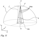
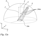
- the at least one associated solid angle and/or the at least one area of the at least one associated solid angle spans the segment S, wherein the segment S corresponds in particular to a segment of a sphere, preferably a conical segment, wherein, for example, half the opening angle, in particular ⁇ /2 and/or ⁇ /2, of the Figure 11 shown segment S is less than 10°, preferably less than 5°, more preferably less than 1°.
- the virtual field sources which are located in particular in and/or on one or more sub-areas of the Figure 11 or 12 shown segment S and/or on the at least one region of the at least one associated solid angle, in at least one direction periodically and/or pseudo-randomly and/or randomly on one or more sub-regions of the one or more sub-regions of the Figure 11 or 12 shown segment S and/or on the at least one region of the at least one associated solid angle.
- the distances between adjacent virtual field sources are between 0.01 mm and 100 mm, in particular between 0.1 mm and 50 mm, preferably between 0.25 mm and 20 mm, in and/or on one or more sub-areas of the one or more sub-areas of the Figure 11 or 12 shown segment S and/or the at least one region of the at least one associated solid angle, and/or that the distances between adjacent virtual field sources are in particular on average between 0.01 mm and 100 mm, in particular between 0.1 mm and 50 mm, preferably between 0.25 mm and 20 mm, in and/or on one or more sub-regions of the one or more sub-regions of the Figure 11 or 12 shown segment S and/or the at least one region of the at least one associated solid angle.
- one or more virtual field sources of the one or more virtual field sources have the form of microsymbols, in particular selected from: letter, portrait, image, alphanumeric character, character, geometric freeform, square, triangle, circle, curved line, outline.
- the lateral dimensions of the microsymbols are between 0.1° and 10°, in particular between 0.2° and 5°.
- a first group of one or more virtual field sources of the one or more virtual field sources cannot be projected onto a screen from a distance of 0.3 m, in particular from 0.15 m to 0.45 m, and/or a second group of one or more virtual field sources of the one or more virtual field sources can be projected onto a screen from a distance of 1.0 m, in particular from 0.8 m to 1.2 m.
- the virtual electromagnetic field emanating from one or more of the virtual field sources, in particular from all of the virtual field sources has the same intensity and/or the same Intensity distribution over the at least one associated solid angle and/or over the at least one region and/or over the at least one segment and/or over the segment S of the at least one associated solid angle.
- the virtual electromagnetic field which emanates from one or more of the virtual field sources, in particular from all of the virtual field sources, has an intensity distribution over the at least one associated solid angle and/or over the at least one region and/or over the at least one segment and/or over the segment S of the at least one associated solid angle, which is distributed in a Gaussian or super-Gaussian manner.
- the virtual electromagnetic field which emanates from two or more of the virtual field sources, in particular from all of the virtual field sources, has different intensities and/or different intensity distributions over the at least one associated solid angle and/or over the at least one region and/or over the at least one segment and/or over the segment S of the at least one associated solid angle.
- the virtual electromagnetic field which emanates from one or more of the virtual field sources, in particular from all of the virtual field sources, to have an isotropic or anisotropic intensity distribution over the at least one associated solid angle and/or over the at least one region and/or over the at least one segment and/or over the segment S of the at least one associated solid angle.
- one or more of the virtual field sources in particular all of the virtual field sources, form a virtual point field source, wherein the virtual point field source preferably emits a virtual spherical wave.
- the virtual electromagnetic field U i comprises one or more wavelengths which lie in particular in the visible spectral range from 380 nm to 780 nm, preferably from 430 nm to 690 nm, wherein one or more, respectively adjacent wavelengths of the one or more wavelengths, preferably in the visible spectral range, are preferably equidistant from one another.
- the virtual electromagnetic field U i comprises one or more wavelengths which are larger by a factor of 2 to 40, in particular by a factor of 3 to 10, preferably by a factor of 4 to 8, than one or more wavelengths of incident electromagnetic radiation.
- the virtual electromagnetic field U i comprises one or more wavelengths which are in particular in the infrared, visible and/or ultraviolet spectral range, wherein one or more, respectively adjacent wavelengths of the one or more wavelengths, preferably in the infrared, visible and/or ultraviolet spectral range, preferably equidistant from each other.
- one or more phase images of the one or more phase images are converted into one or more virtual structure profiles, preferably linearly converted into a virtual structure profile, wherein a phase value of 0 corresponds to the minimum depth and a phase value of 2 ⁇ corresponds to the maximum depth of the formed one or more structures of one or more pixels of the two or more pixels of the at least one pixel array.
- the virtual structure profile of one or more virtual pixels of the two or more virtual pixels of the at least one virtual Pixel array is formed by means of laser exposure and development on a photoresist coated plate and/or by means of electron beam lithography as the one or more structures of one or more pixels of the two or more pixels of the at least one pixel array.
- one or more structures comprised or formed in one or more pixels of the two or more pixels of the at least one pixel array have an optical depth, in particular an optical depth in air, of half the average wavelength of the virtual electromagnetic field and/or the virtual total electromagnetic field.
- a method for producing a security document in particular the security document 1d, preferably comprising one or more layers, further preferably comprising one or more optically variable elements, particularly preferably the optically variable elements 1a, is characterized by the following steps: Applying and/or introducing one or more optically variable elements as a laminating film and/or as an embossing film onto the security document and/or onto one or more layers of the security document and/or into the security document and/or into one or more layers of the one or more layers of the security document.
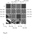
- the Figure 2 shows a pixel array in plan view comprising sixteen pixels 2aa-2dd, wherein the pixels 2aa-2dd are arranged as a 4x4 matrix having four rows and four columns.
- the first row comprises the pixels 2aa, 2ab, 2ac, 2ad along the x direction
- the second row comprises the pixels 2ba, 2bb, 2bc, 2bd along the x direction
- the third row comprises the pixels 2ca, 2cb, 2cc, 2cd along the x direction
- the fourth row comprises the pixels 2da, 2db, 2dc, 2dd along the x direction.
- the first column comprises the pixels 2da, 2ca, 2ba, 2aa along the y direction
- the second column comprises the pixels 2db, 2cb, 2bb, 2ab along the y direction
- the third column includes pixels 2dc, 2cc, 2bc, 2ac along the y direction
- the fourth column includes pixels 2dd, 2cd, 2bd, 2ad along the y direction.
- the pixels 2aa-2dd shown have the same lateral dimensions ⁇ X along the x direction and the same lateral dimensions ⁇ Y along the y direction, each forming square shapes in the plane spanned by the x and y directions.
- one or more or all pixels of the one, two or more pixels 2aa-2dd to form identical or different shapes, in particular in the plane defined by the pixel array 2 and/or in the plane defined by the x and y directions, which are preferably each selected from: circular area, egg-shaped area, elliptical area, triangular area, square area, rectangular area, polygonal area, annular area, free-form area, wherein the two or more pixels, in the case of the selection of the shape of the pixels as a circular area and/or egg-shaped area, in particular each have one or more adjacent background areas, which preferably also border or do not border adjacent pixels.
- the shape of the pixels varies in particular polygonally, randomly or pseudo-randomly. More preferably, the at least one pixel array, in particular the pixel array 2, comprises two or more pixels, which preferably comprise different shapes of the above shapes and/or preferably have different variations of the shapes of the above variations of shapes.
- one or more or all pixels of the two or more pixels 2aa-2dd have different lateral dimensions in different directions, in particular in the different directions x and y, in particular in the plane defined by the pixel array 2 and/or in the plane defined by the directions x and y.
- one or more or all pixels of the two or more pixels 2aa-2dd in particular in the plane defined by the pixel array 2 and/or in the plane defined by the directions x and y, occupy different areas and/or overlap each other and/or do not overlap each other.
- the arrangement of the pixels 2aa-2dd in the pixel array 2 can follow a periodic function.
- the centers of the pixels in a row or column of the pixel array can be arranged such that the centers of the pixels of adjacent pixels are preferably equally spaced along a direction defined by the column or row.
- the Figure 2 The pixels 2aa-2dd shown each have the same distances from one another along the directions x or y, whereby this particularly applies to neighboring pixels of the pixels 2aa-2dd.
- one or more or all pixels of the pixels 2aa-2dd are arranged non-periodically or in particular randomly or pseudo-randomly in the pixel array 2 and/or along one or more directions and/or in the plane spanned or defined by the directions x and y.
- a center point of the pixels or a geometric center of gravity of the pixels is understood to be the area center of gravity, especially in the case of flat pixels, which is determined in particular by averaging all points of the underlying pixel.
- a non-periodic arrangement of pixels has the advantage that disturbing diffraction effects, which arise due to the size or shapes and/or lateral dimensions of the pixels, can be reduced or suppressed, in particular completely suppressed.
- the lateral dimensions of one or more pixels of the pixels 2aa-2dd along at least one direction, in particular along the x direction and/or along the y direction are between 5 ⁇ m and 500 ⁇ m, in particular between 10 ⁇ m and 300 ⁇ m, in particular between 20 ⁇ m and 150 ⁇ m.
- Such lateral dimensions have the advantage that pixels with these orders of magnitude of lateral dimensions are not or hardly optically resolvable for the eye of a human observer, especially at a usual or normal reading distance of approximately 300 mm. At the same time, the pixels are large enough that the intended microstructures can appear achromatic.
- the pixel size and/or one or more lateral dimensions of one or more pixels of the pixels 2aa-2dd in the at least one pixel array 2 may vary or not vary in one or more directions, in particular in one or both directions of the x and y directions, preferably in regions, non-periodically, periodically, pseudorandomly or randomly.
- the pixel sizes in at least one pixel array vary in at least one spatial direction by a maximum of ⁇ 70% around a mean value, preferably by a maximum of ⁇ 50%.
- one or more lateral dimensions of one or more pixels of the two or more pixels 2aa-2dd in the at least one pixel array 2 vary in one or more spatial directions, in particular in one or both directions of the x and y directions, in the at least one pixel array 2 at least in regions by a maximum of ⁇ 70%, preferably a maximum of ⁇ 50%, around a mean value, wherein the mean value in one or more directions is in particular between 5 ⁇ m and 500 ⁇ m, in particular between 10 ⁇ m and 300 ⁇ m, in particular between 20 ⁇ m and 150 ⁇ m.
- one or more pixels of the pixels 2aa-2dd in the at least one pixel array 2 are arranged periodically, non-periodically, fractally, randomly and/or pseudorandomly in the at least one pixel array 2, in particular at least in regions.
- the Figure 3 shows this in the Figure 2 shown pixel array 2 comprising the pixels 2ca, 2cb, 2cc, 2cd, along the section Q in a cross section.
- the pixel 2ca comprises the structure 3ca
- the pixel 2cb comprises the structure 3cb
- the pixel 2cc comprises the structure 3cc
- the pixel 2cd comprises the structure 3cd.
- the structures 3ca, 3cb, 3cc and 3cd are applied, applied and/or molded onto a substrate 10, wherein the substrate in particular has one or more layers.
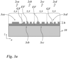
- the Figure 3a shows another embodiment of the Figure 2 shown pixel arrays 2 comprising the pixels 2ca, 2cb, 2cc, 2cd, along the section Q in a cross section.
- the pixel 2ca comprises the structure 3ca
- the pixel 2cb comprises the structure 3cb
- the pixel 2cc comprises the structure 3cc
- the pixel 2cd comprises the structure 3cd.
- the structures 3ca, 3cb, 3cc and 3cd are applied, applied and/or molded onto a substrate 10, wherein the substrate in particular has one or more layers.
- the structures 3ca, 3cb, 3cc and 3cd are in particular binary structures with a first distance or a uniform structure height h.
- binary structures 3ca, 3cb, 3cc and 3cd or binary microstructures preferably comprising one or more structural elements, in particular a base surface GF and several structural elements, which preferably each have an element surface EF that is raised relative to the base surface GF and preferably a flank arranged between the element surface EF and the base surface GF, wherein in particular the base surface GF of the structure 3ca, 3cb, 3cc and 3cd defines a base plane spanned by coordinate axes x and y, wherein preferably the element surfaces EF of the structural elements each run essentially parallel to the base plane GF and wherein preferably the element surfaces EF of the structural elements and the base surface GF are spaced apart in a direction perpendicular to the base plane in the direction of a coordinate axis z, in particular with a first distance h, which is preferably selected such that in particular by interference of the light reflected on the base surface GF and the element surfaces EF in incident light and
- the optically variable element 1a comprises one or more layers, wherein in particular the at least one pixel array 2 is arranged on or in at least one layer of the one or more layers and wherein preferably one or more layers of the one or more layers are selected from: HRI layer, in particular layer comprising HRI and/or LRI lacquer layer, metal layer, interference layer, in particular interference layer sequences, preferably HLH or HLHLH, more preferably Fabry-Perot three-layer system or multi-layer system, liquid crystal layer, color layer, in particular translucent color layer.
- each of the structures 3ca, 3cb, 3cc, 3cd has a limited maximum structure depth ⁇ z, in particular a maximum structure depth, which in the Figure 3 is in particular the same for all structures 3ca, 3cb, 3cc, 3cd in the corresponding pixels 2ca, 2cb, 2cc, 2cd.
- one or more structures of the one or more structures 3ca, 3cb, 3cc, 3cd have a limited maximum structure depth ⁇ z, wherein the maximum structure depth ⁇ z is in particular less than 35 ⁇ m, preferably less than 20 ⁇ m, more preferably less than or equal to 15 ⁇ m, even more preferably less than or equal to 7 ⁇ m, in particular preferably less than or equal to 2 ⁇ m.
- the thickness or the total thickness of the optically variable element 1a comprising the at least one pixel array 2 is kept compatible for use in security documents 1d, in particular on banknotes, ID cards or passports.
- the total thickness of film-based optically variable elements 1a is less than 35 ⁇ m. It is preferred that the total thickness is less than 20 ⁇ m, in order to advantageously suppress bending of banknotes due to an applied film comprising one or more optically variable elements 1a. Furthermore, it is possible to limit the limited maximum structure depth of all structures 3ca, 3cb, 3cc, 3cd of the corresponding pixels 2ca, 2cb, 2cc, 2cd in such a way that the structures 3ca, 3cb, 3cc, 3cd are preferably applied, applied and/or molded using a replication method.
- one or more structures of the one or more structures 3ca, 3cb, 3cc, 3cd are formed such that the limited maximum structure depth ⁇ z of the one or more structures 3ca, 3cb, 3cc, 3cd for more than 50% of the pixels, in particular for more than 70% of the pixels, preferably for more than 90% of the pixels, of the at least one pixel array 2 is less than or equal to 15 ⁇ m, in particular less than or equal to 7 ⁇ m, preferably less than or equal to 2 ⁇ m.
- one or more structures of the one or more structures 3ca, 3cb, 3cc, 3cd are formed such that the maximum structure depth ⁇ z of the one or more structures for all pixels is less than or equal to 15 ⁇ m, in particular less than or equal to 7 ⁇ m, preferably less than or equal to 2 ⁇ m.
- one or more structures of the one or more structures 3ca, 3cb, 3cc, 3cd have a grating period in particular smaller than half, preferably smaller than a third, more preferably smaller than a quarter, of the maximum lateral dimension of the pixels 2ca, 2cb, 2cc, 2cd, preferably each of the pixels 2ca, 2cb, 2cc, 2cd.
- one or more structures of the one or more structures 3ca, 3cb, 3cc, 3cd are different or similar or the same or identical to one another.
- the Figure 4 shows this in the Figure 2 shown pixel array 2, except that each of the pixels 2aa-2dd is assigned a corresponding structure 3aa-3dd or that each of the pixels 2aa-2dd comprises a corresponding structure 3aa-3dd, wherein the structures 3aa-3dd are designed as hologram-like structures, in particular those which achromatically image, diffract and/or scatter incident light.
- one or more or all of the structures of structures 3aa-3dd have different optical properties from each other.
- one or more structures of the one or more structures 3aa-3dd are assigned to each pixel of the pixels 2aa-2dd of the at least one pixel array 2, wherein the one or more structures assigned to a pixel image, diffract and/or scatter incident electromagnetic radiation in one or more predetermined solid angles, wherein in particular the one or more predetermined solid angles are each assigned a direction, preferably a predetermined direction.
- one or more structures of the one or more structures 3aa-3dd and/or one or more associated structures of the one or more associated structures 3aa-3dd are in one or more solid angles of the one or more solid angles and/or one or more predetermined solid angles of the one or more predetermined solid angles, which in particular differ from one another, wherein one or more solid angles of the one or more solid angles and/or predetermined solid angles of the one or more predetermined solid angles projected onto a sphere arranged around a pixel, in particular a unit sphere with a unit radius of 1, form one or more, in particular identical or different, shapes, which are preferably each selected from: circular area, elliptical area, triangular area, square area, rectangular area, polygonal area, annular area, wherein in particular one or more shapes of the one or more shapes are open or closed and/or consist of one or more partial shapes, and wherein preferably at least two partial shapes are connected to one another or superimposed.
- the Figure 5 shows this in the Figure 2 shown pixel array 2, except that each of the pixels 2aa-2dd is assigned a corresponding structure 3aa-3dd or that each of the pixels 2aa-2dd comprises a corresponding structure 3aa-3dd, wherein the structures 3aa-3dd are designed as grating structures which achromatically image, diffract and/or scatter incident light.
- the grating structures are linear grating structures which preferably have a blaze-like grating profile.
- the achromatically diffractive grating structures in one or more pixels of the pixels 2aa-2dd in the at least one pixel array 2 are superimposed with further microstructures and/or nanostructures, in particular linear grating structures, preferably cross grating structures, more preferably subwavelength grating structures.
- the one or more structures of the one or more structures 3aa-3dd which are designed as achromatically diffractive grating structures, preferably as blazed gratings, in particular have a grating period of greater than 3 ⁇ m, preferably greater than 5 ⁇ m, and/or in particular each pixel of the pixels 2aa-2dd comprises at least two grating periods of the achromatically diffracting structures.
- each pixel of the pixels 2aa-2dd is assigned a corresponding structure 3aa-3dd or that each pixel of the pixels 2aa-2dd comprises a corresponding structure 3aa-3dd
- the structures 3aa-3dd are designed as Fresnel microlens structures and/or partial areas or sections of Fresnel microlens structures
- the grid lines of the Fresnel microlens structures are designed as curved grid lines and/or have grid lines with varying grid periods and/or wherein in particular each pixel of the two or more pixels comprises at least two grid periods, preferably in at least one spatial direction.
- the Fresnel microlens structures are designed as blazed gratings, wherein the grating lines are in particular curved and/or wherein the grating period preferably varies.
- one or more or all of the structures are less preferably designed as micromirrors and/or microprisms, in particular less preferably as achromatically refractively imaging microstructures.
- more than 70% of the pixels, in particular more than 90% of the pixels, of the pixels 2aa-2dd in the at least one pixel array 2 have one or more structures of the one or more structures 3aa-3dd, which have a number of at least 2 elevations, in particular at least 3 elevations, preferably at least 4 per pixel.
- one or more structures of the one or more structures have a number of at least 2 elevations, in particular at least 3 elevations, preferably at least 4 elevations per pixel.
- At least two grating periods of the structures designed as blazed gratings and/or Fresnel microlens structures are located in at least one pixel, wherein the grating period is preferably smaller than half the maximum lateral dimension of each pixel.
- one or more structures of the one or more structures 3aa-3dd are designed as chromatic grating structures, in particular as linear gratings, preferably as linear gratings with a sinusoidal profile, and/or as nanotext and/or as mirror surfaces. This makes it possible in particular to integrate colored design elements and/or hidden features into the achromatically appearing pixel array.
- the Figure 7 shows this in the Figure 2 shown pixel array 2, except that the pixels 2aa, 2ad and 2cc each have a linear grid 30aa, 30ad and 30cc, respectively, in particular comprising a sinusoidal profile.
- one or more structures of the one or more structures 3aa-3dd are designed as subwavelength gratings, in particular as linear subwavelength gratings, wherein preferably the grating period of the subwavelength gratings, in particular of the linear subwavelength gratings, is less than 450 nm and/or wherein in particular at least one such pixel array has an optically variable effect that can be detected by a viewer when tilting and/or rotating the optically variable element and/or the at least one pixel array.
- an optically variable effect involves one or more icons, logos, images and/or other motifs that can be detected by a viewer and/or a sensor, which preferably light up when the optically variable element 1a is tilted sharply.
- one or more structures of the one or more structures 3aa-3dd are provided, in particular at least partially, with a metal layer and/or absorb incident electromagnetic radiation, wherein preferably one or more pixels of the two or more pixels are detectable in reflection, preferably in direct reflection, for an observer in dark gray to black.
- the Figure 8 shows this in the Figure 2 shown pixel array 2, except that the pixels 2aa, 2ad and 2cc each have a light-absorbing, in particular incident light-absorbing, microstructure 31aa, 31ad or 31cc, wherein these absorbing microstructures 31aa, 31ad or 31cc preferably appear dark gray to black to an observer and/or a sensor.
- the absorbing microstructures 31aa, 31ad or 31cc are designed as subwavelength cross gratings, in particular with a grating period of less than or equal to 450 nm, preferably less than or equal to 350 nm.
- Such pixels with microstructures that appear dark gray to black make it possible in particular to increase the contrast of the appearance of the pixel array and, for example, to create the illusion of shadows.
- one or more structures of the one or more structures 3aa-3dd are formed as microstructures which absorb light, in particular absorb incident light, and/or appear colored to a viewer and/or a sensor upon normal observation or in direct reflection.
- the pixels that appear dark to represent, for example, a shadow expected by a viewer with more contrast.
- one or more structures of the one or more structures 3aa-3dd have an HRI layer, wherein in particular the pixels which have the one or more structures can be detected in color in reflection for a viewer and/or sensor.
- microstructures in a number of pixels of the pixels 2aa-2dd predetermined by a design, which, in particular when at least partially coated with at least one high-refractive dielectric layer, in particular at least one HRI layer, preferably appear colored, for example red or green, when detected by a viewer and/or a sensor when viewed normally or in direct reflection.
- Such microstructures are preferably designed as linear subwavelength gratings, wherein the colored pixels comprising the microstructures of this type For example, in a portrait, generate green pupils that can be detected by a viewer and/or sensor.
- the Figure 9 shows a section of a pixel array 2 comprising sixteen pixels 2aa-2dd in a perspective top view, wherein the pixel array extends in the plane spanned by the directions x and y. Furthermore, the direction of incidence of an incident light 6 and the directions of emergence of emerging light 20aa-20dd for the corresponding pixels 2aa-2dd are shown in the Figure 9 shown.
- the outgoing light 20aa-20dd radiates in particular into the half-space which is defined in particular by the plane of the pixel array, with the incident light 6 preferably incident from a direction of this half-space.
- the incident light 6 is in particular achromatically diffracted in the corresponding directions of the outgoing light 20aa-20dd as outgoing light 20aa-20dd.
- the incident light 6 is in particular pseudo-randomly imaged, diffracted and/or scattered in any spatial direction as outgoing light 20aa-20dd in or at each pixel 2aa-2dd, preferably individually in or at each pixel 2aa-2dd comprising a respective structure 3aa-3dd.
- one or more structures of the one or more structures 3aa-3dd preferably in the corresponding pixels of the pixels 2aa-2dd, image, diffract and/or scatter incident electromagnetic radiation, in particular incident light 6, pseudo-randomly or randomly in all spatial directions such that one or more pixels of the pixel array 2 can be detected in reflection for an observer and/or a sensor, preferably isotropically white, preferably isotropically achromatic.
- the Figure 10 shows an enlarged section of the Figure 9 shown pixel array 2, which comprises, for example, a pixel 2ad comprising light-imaging, diffracting and/or scattering structures 3ad, which reflects incident light or incident electromagnetic radiation as outgoing light 20ad in a predetermined direction and/or in a predetermined solid angle images, diffracts and/or scatters.
- the paths and/or propagation directions of the outgoing light 20ad preferably run parallel to one another.
- the light incident on the pixel array 2 or the incident electromagnetic radiation can be diffracted and/or scattered as outgoing light 2aa-2dd only in at least one area, in particular one or more at least partially connected or non-connected and/or at least partially overlapping or non-overlapping areas, of one or more predetermined solid angles, pseudo-randomly or randomly imaged, diffracted and/or scattered.
- This advantageously increases the brightness and/or intensity of the outgoing light or the outgoing electromagnetic radiation in these areas and/or predetermined solid angles, wherein in particular the effect that can be detected by a viewer and/or sensor, preferably a visual effect, is better detectable in low lighting conditions.
- the opening angles of the predetermined solid angles are preferably restricted to less than +/-10°, preferably less than +/-5°, more preferably +/-3°, in particular in at least one direction.
- Structural parameters Areas Preferred areas Particularly preferred areas Lateral dimensions of a pixel and/or ⁇ X and/or ⁇ Y 5 ⁇ m to 500 ⁇ m 10 ⁇ m to 300 ⁇ m 20 ⁇ m to 150 ⁇ m Limited maximum structure depth ⁇ 15 ⁇ m ⁇ 4 ⁇ m ⁇ 2 ⁇ m Distances between neighboring virtual field sources 0.001 m to 100 m 0.1 m to 5 m 0.25 to 2 m Microlens focal length 0.04mm to 5mm 0.06mm to 3mm 0.1mm to 2mm Number of elevations per pixel ⁇ 2 ⁇ 3 ⁇ 4
- the Figure 11 shows an enlarged section of the Figure 6 shown pixel array 2 comprising the pixel 2da, in which at least one structure 3da is formed as a Fresnel microlens structure, wherein incident light or incident electromagnetic radiation is imaged, diffracted and/or scattered, in particular focused, by the structure 3da onto one or more points and/or one or more surfaces in space perpendicular to the plane spanned by the pixel array 2 and/or to the plane spanned by the directions x and y.
- the Figure 11 is merely schematic and not to scale.
- one or more structures of the one or more structures are designed as a cylindrical lens, wherein in particular the focal length of the one or more structures is infinitely large.
- the sizes and/or lateral dimensions of the pixels and/or the associated solid angles determine the corresponding focal lengths.
- the Figure 12 shows an enlarged section of the Figure 6 shown pixel array 2 comprising the pixel 2da, in which at least one structure 3da is molded as a Fresnel microlens structure, wherein incident light or incident electromagnetic radiation from the structure 3da is imaged, diffracted and/or scattered, in particular focused, onto one or more points or one or more surfaces in space, in particular not perpendicular to the plane spanned by the pixel array 2 and/or to the plane spanned by the directions x and y, but at an angle ⁇ to the surface normal f of the above planes in a direction R.
- the radius of the sphere E is in particular equal to the focus height f.
- the Fresnel microlens structure is preferably calculated or designed for a wavelength of 550 nm, in particular a wavelength range from 450 nm to 650 nm, of the incident light.
- the Figure 12a shows an enlarged section of the Figure 6 shown pixel array 2 comprising the pixel 2da, in which at least one structure 3da as Fresnel microlens structure is molded, wherein incident light or incident electromagnetic radiation is imaged, diffracted and/or scattered, in particular focused, by the structure 3da onto one or more points or one or more surfaces in space, in particular not perpendicular to the plane spanned by the pixel array 2 and/or to the plane spanned by the directions x and y, but at an angle ⁇ to the surface normal f of the above planes in a direction R.
- structure 3da as Fresnel microlens structure
- each of the one or more virtual pixels of the two or more virtual pixels of the at least one virtual pixel array is assigned at least one solid angle.
- the half opening angle of the Figure 11 shown associated solid angle which is limited by the lines 20da, are for example ⁇ /2 and ⁇ /2.
- a virtual pixel is assigned to each pixel 2da.
- one or more virtual field sources in and/or on the Figures 11 , 12 and 12a shown segments S are each arranged at first distances from the respective virtual pixels, wherein the position and/or orientation of the respective virtual pixel in the Figures 11 , 12 or 12a preferably each correspond to the position and/or orientation of the Figures 11 , 12 and 12a shown respective pixel 2da.
- one or more virtual electromagnetic fields are generated from the one or more virtual field sources, in particular arranged in the Figures 11 , 12 and 12a shown segments S, at a predetermined distance from one or more virtual pixels of the two or more virtual pixels of the at least one virtual pixel array in and/or on the one or more virtual pixels of the two or more virtual pixels of the at least one virtual pixel array and/or in and/or on the area, in particular plane, spanned by the at least one virtual pixel array.
- one or more phase images for one or more virtual pixels of the two or more virtual pixels of the at least one virtual pixel array are calculated from a virtual electromagnetic total field consisting of the superposition of the one or more virtual electromagnetic fields in and/or on the one or more virtual pixels of the two or more virtual pixels of the at least one virtual pixel array and/or in and/or on the area, in particular the plane, spanned by the at least one virtual pixel array, wherein the respective planes are in the Figures 11 , 12 and 12a in particular correspond to the planes spanned by the respective pixels 2da.
- virtual structure profiles for the one or more virtual pixels of the two or more virtual pixels of the at least one virtual pixel array are calculated from the one or more phase images.
- the virtual structure profiles of the two or more virtual pixels of the at least one virtual pixel array are arranged in and/or on a substrate as at least one pixel array comprising two or more pixels, wherein the respective Figures 11 , 12 and 12a shown pixels 2da of the at least one pixel array have one or more structures 3da, designed to provide an optically variable element.
- a small and/or smaller opening angle of the predetermined solid angles generates a 3D effect that can be perceived by a viewer and/or sensor with a smooth-appearing surface of the portrait or a motif.
- a large and/or larger opening angle of the solid angles generates a 3D effect that can be perceived by a viewer and/or sensor with surfaces of the portrait or a motif that appear very matt.
- This controlled mattness can be used as a design element, for example to make the top of a mountain shown as a 3D effect appear to be covered in snow.
- the opening angle is in the range between 0.5° and 70° and preferably between 1° and 60°.
- the upper part of the Figure 13b shows five sections 91, 92, 93, 94, 95 of a 3D model of a lion, with the opening angle increasing from 1° to 60° from left to right. All pixels bend the incident light in the direction intended for the pixel, particularly with approximately the same opening angle.
- Section 91 of the lion on the far left has a reflective virtual surface
- section 95 of the lion on the far right has a satin-matt surface.
- the three sections 92, 93, 94 of lions in between show intermediate values of mattness.
- the lower part of the Figure 13b shows this with a 3D model of a lion 96, 97, where on the left in a K-shaped part of the lion 96 the dullness is greater than in the rest of the lion and in the right lion 97 in the K-shaped part of the lion the dullness is less than in the rest of the lion.
- the opening angle in the left lion 96 in the areas without a K-shaped part is 1° and in the right lion 97 the opening angle is 15°.
- the K-shaped part in the left lion 96 has an opening angle of 60° and the K-shaped part in the right lion 97 has an opening angle of 1°.
- the lower parts of the Figure 13 show micrographs of sections of the underlying pixel arrays of the upper part of the Figure 13 shown portraits in different magnifications of the respective areas.
- the structures encompassed by the pixels arranged in the pixel arrays can be captured.
- a change in the predetermined solid angles in which the pixels image, diffract and/or scatter the incident light preferably leads to a significant change in the underlying structures and, with increasing opening angles, in particular to a significant deviation from ordered or periodic structures.
- the Figure 14 shows an example of such a change in the structure of a selected pixel of the Figure 13 shown designs, where the structure changes from left to right with increasing opening angle.
- the structures in the pixels are preferably selected such that the electromagnetic radiation incident in the predetermined area of the 3D effect is essentially preferably directed into the image and/or diffract and/or scatter in a predetermined direction.
- the opening angle is selected depending on the direction.
- the left part 98 of the Figure 13c shows a design comprising a 3D model of the portrait of the mathematician and physicist Carl Friedrich Gauß, whereby, when viewed normally, the face essentially preferentially images and/or bends and/or scatters incident electromagnetic radiation in the direction of a viewer.
- This area of the portrait appears particularly 3D-curved and dull-light.
- the other areas of the portrait appear preferably dark to barely perceptible.
- the face after rotating the optically variable element by 90° clockwise, as in the right part 99 of the Figure 13c shown, the face appears preferably dark to barely perceptible and the other areas of the portrait appear particularly 3D-curved and dull-light.
- the opening angle is preferably in a range between 0.5° and 70°, more preferably between 1° and 60°.
- the structures formed as an achromatic microstructure are superimposed with further microstructures and/or nanostructures in one or more or all pixels of the two or more pixels of the at least one pixel array.
- further microstructures and/or nanostructures are linear grating structures, cross grating structures, in particular subwavelength grating structures.
- Examples of such zero-order diffraction color effects are in particular so-called resonant gratings in the case of an HRI coating or gratings with effects based on plasmon resonance in the case of metal coatings, in particular aluminum coating.
- the optical effect of the at least one pixel array is created in particular in the color of the superimposed subwavelength grating structure effects.
- the grating period for the resonant gratings coated with HRI is preferably in the range of 200 nm to 500 nm.
- the subwavelength grating structures of the resonant gratings are preferably linear gratings.
- the Figure 15 shows an arrangement of pixels of a pixel array 2 comprising corresponding structures, which is designed in particular such that a fine line movement (“movement of thin or fine lines") that can be detected by a viewer and/or sensor is generated, wherein the width of the detectable lines is preferably dependent on the sizes and/or lateral dimensions of the pixels.
- the structures in the individual linearly arranged groups of pixels G are designed such that they image in particular incident light in different spatial directions and/or in different predetermined solid angles, wherein preferably by tilting such an optically variable element depending on the viewing situation and/or viewing direction and/or the incident light and/or the direction of incidence of the incident light, adjacent linearly arranged groups of pixels G light up one after the other, in particular achromatically, in particular depending on the tilting direction.
- one or more linearly arranged groups of pixels can be omitted and/or to light up at a random angle, with the lighting up of the linearly arranged groups of pixels preferably being generated in an arbitrary sequence.
- achromatic fine line morphing effects (“movement and/or shape change thin or fine lines”) can be generated, which can preferably be detected by an observer and/or a sensor.
- a first group of structures which image, diffract and/or scatter incident light, in particular achromatically, for example computer-generated hologram structures are formed, whereby these structures of the first group of structures achromatically image, diffract and/or scatter incident light at a first inclination angle of approximately 30° to the surface of the plane spanned by the optically variable element.
- the pixels of the first group of pixels form a first motif.
- a second group of structures which image, diffract and/or scatter incident light in particular achromatically for example computer-generated hologram structures, whereby these structures of the second group of structures achromatically image, diffract and/or scatter incident light at a second angle of inclination of approximately 5° to the surface of the plane spanned by the optically variable element.
- the pixels of the second group of pixels form a second motif.
- one or more structures of the one or more structures and/or the structures assigned to a pixel of the two or more pixels of the at least one pixel array image diffract and/or scatter electromagnetic radiation, in particular incident electromagnetic radiation, in a solid angle, in particular a point-shaped solid angle.
- one or more structures of the one or more structures and/or one or more pixels of the two or more pixels of the at least one pixel array comprising one or more associated structures of the one or more associated structures are associated with two or more groups of structures and/or two or more groups of pixels, in particular wherein the groups of the two or more groups of structures and/or the groups of the two or more groups of pixels differ from one another.
- two or more groups of structures of the two or more groups of structures and/or two or more groups of pixels of the two or more groups of pixels to image, diffract and/or scatter electromagnetic radiation, in particular incident electromagnetic radiation, into the same or different solid angles and/or predetermined solid angles, in particular point-shaped solid angles and/or predetermined solid angles, preferably different-shaped solid angles and/or predetermined solid angles.
- two or more groups of structures of the two or more groups of structures and/or two or more groups of pixels of the two or more groups of pixels provide optically variable information comprising a 3D effect.
- first motif may appear light and the second motif to appear dark if the optically variable element is detected in particular from the predetermined solid angle corresponding to the first angle of inclination. It is also possible for the optically variable element to be aligned after tilting with respect to a viewer and/or sensor in such a way that the optically variable element can be detected in particular from the predetermined solid angle corresponding to the second angle of inclination, with the second motif preferably appearing light and the first motif appearing dark. Such an effect is preferably also referred to as an image flip effect.
- the structures prefferably, it is possible for the structures to image, diffract and/or scatter the incident light in three or more predetermined solid angles, with each of the predetermined solid angles being assigned in particular different motifs, in particular images.
- a viewer and/or sensor generates an illusion of a continuous and/or erratic movement of a motif, which appears in particular with corresponding movement, rotation and/or tilting of the optically variable element.
- the underlying pixel array is divided into parts which generate the respective motifs and/or one or more pixels of the two or more pixels of the pixel array are each divided into parts or subpixels which each have different structures which image, diffract and/or scatter the incident light in the predetermined solid angles to generate the corresponding motifs.
- one or more pixels of the two or more pixels are each divided into three, in particular four, more preferably five, parts or subpixels, wherein the parts or subpixels particularly preferably each have different structures.
- a changing form of a motif for example a transformation from one motif, for example the letter sequence "CH”, to another motif, for example the Swiss cross, which can be detected by a viewer and/or a sensor, whereby in particular visually enlarging or shrinking outlines of a motif are possible.
- one or more pixels of the two or more pixels of the at least one pixel array to image, diffract and/or scatter at least two views of a subject in different predetermined spatial angles, wherein at least one stereo image of the subject can be captured, in particular, by an observer and/or sensor at at least one predetermined distance.
- the Figure 16 shows on the left side the Figure 1 shown strip-shaped security element 1b', wherein a viewer and/or sensor, when viewing the security element 1b', in particular in incident light and/or transmitted light, detects movement effects and/or 3D elements that optically project virtually in the viewing direction and/or recede from the viewing direction.
- the security document 1d has one or more further optically variable elements in or outside the strip-shaped area 1b'.
- the strip-shaped security element 1b further comprises two optically variable elements 1a, which in particular each have at least one pixel array comprising two or more pixels and are arranged on the right-hand side of the Figure 16 are shown in magnification.
- strip-shaped security element 1b' comprises several security elements 8, which are designed as the number sequence "45”, two cloud-like motifs, an airplane-shaped motif, a sailing ship-shaped motif and a word sequence "UT" crossed by two horizontal lines.
- the sun-shaped optically variable element 1a shown at the top right generates an optical effect in such a way that the emerging light from the curved surface of the sun 9a appears to be preferably reflected for an observer and/or sensor.
- the sun 9a preferably protrudes in a seemingly tangible manner, in particular as tangible for an observer. or expected to be haptically perceptible, from the plane and/or surface spanned by the optically variable element 1a, although the security element is preferably completely even and/or flat.
- the optically variable element shown at the bottom right comprises a pixel array which generates the illusion, in particular the optical illusion, of water 9b moving in waves, particularly for a viewer and/or sensor. When the optically variable element 1a is tilted, a brightness band which moves from left to right and/or in the opposite direction preferably appears to a viewer and/or sensor.
- one or more structures of the one or more structures provide an optically variable effect when the element and/or the at least one pixel array is bent, wherein in particular a first motif can be detected in a non-bent state of the element and/or the at least one pixel array and a second motif can be detected in a bent state of the element and/or the at least one pixel array.
- an image flip is also possible for an image flip to be detected by a viewer and/or a sensor in such a way that a first motif can be detected in the non-bent state and a second motif in the bent state.
- the virtual pixel array is provided in a bent state for calculating the corresponding structures in the virtual pixels and the virtual electromagnetic fields, which are preferably emitted by one or more virtual point field sources, are preferably calculated on the bent virtual pixel array. This in particular ensures that the one or more predetermined solid angles in which the structures image, diffract and/or scatter the incident light are compensated accordingly by the local curvature of the optically variable element, preferably in the bent state.
- the motif is preferably imaged, diffracted and/or scattered in the one or more predetermined solid angles in such a way that scattered in such a way that the subject is preferably not completely perceptible to a viewer and/or sensor and/or is only optically distorted.
- optically variable elements it is possible for a viewer and/or sensor to detect one or more of the following effects generated by one or more optically variable elements, in particular the following optical effects generated by one or more optically variable elements: One or more effects in reflection; one or more effects in transmission; combination of the above effects in reflection and in transmission, such as different motion effects in reflection and transmission, wherein in particular 50% of the pixels and/or subpixels of at least one pixel array are used for the respective effect in reflection or transmission; one or more effects for a bent or unbent state of one or more optically variable elements of the one or more optically variable elements.
- phase jumps of 2 ⁇ 180° in reflection and 1 ⁇ 360° in transmission occur.
- phase jump is preferably only exact at one wavelength, with the corresponding effect preferably being color-selective around this wavelength. The effect therefore appears to a viewer and/or sensor in particular in a clearly defined color. All of the above effects, in particular all of the above optical effects, can be implemented in this way with a correspondingly defined color, for example.
- the Figure 17 shows, by way of example, an achromatic arc comprising a plurality of light points 200, which moves up and/or down along the direction R', in particular when tilting forwards and/or backwards or when tilting along the direction R', of the optically variable element or moves up and/or down along the direction R' in the figure plane spanned by the directions x and y.
- the structures in the pixels of the underlying pixel array are designed in particular in such a way that incident When the optically variable element is tilted by -30° to +30° out of the figure plane spanned by the directions x and y, light preferably creates the illusion of a moving bright arc for an observer and/or sensor.
- the Figure 18 shows in the upper part a first enlarged section and in the lower part a second, in particular even further enlarged, section of the underlying pixel array comprising pixels with corresponding structures.
- the outlined pixel 2e having the structure 3e has a lateral dimension of 50 ⁇ m in the x and y directions.
- the Figure 19 shows, in a schematic perspective representation, a movement sequence of an achromatic, arc-shaped motif 9c that can be detected by an observer B and/or a sensor S, which moves in the plane spanned by the optical element 1a, in particular along the direction R", wherein the structures of the pixel array 2 contained in the optically variable element 1a image, diffract and/or scatter the incident light 20 in the direction of the observer B and/or sensor S.
- the Figure 20 shows a 3D object in the form of a snail shell 9d that protrudes achromatically for a viewer and/or sensor from the figure plane, in particular from the plane spanned by the x and y directions.
- the structures in the pixels of the underlying pixel array are designed in such a way that incident light creates the illusion of the 3D object. When tilting back and forth, as well as left and right, light and shadow move across the snail for a viewer and/or sensor.
- the Figure 21 shows in the upper part a first enlarged section and in the lower part a second, in particular even further enlarged section of the Figure 20 shown snail shell 9d underlying pixel array comprising pixels with corresponding structures.
- the outlined pixel 2f The structure 3f has a lateral dimension of 50 ⁇ m in the x and y directions.
- the Figure 22 shows a design comprising a 3D model of the portrait 9e of the mathematician and physicist Carl Friedrich Gauss in 28 different variants and the Figure 23 shows an enlarged section of the Figure 22 , whereby the structures in the pixels of the underlying pixel array are particularly formed as Fresnel microlens structures, which were used to generate the variants.
- the portraits in the first row show from left to right an increasing variation in the 3D effect strength that can be perceived by a viewer and/or sensor.
- the first four portraits in the subsequent rows show from left to right an effect based on the corresponding portrait based on structures with a structure depth of 2 ⁇ m, and the last three portraits in the subsequent rows show from left to right an effect based on the corresponding portrait based on structures with a structure depth of approximately 1 ⁇ m.
Landscapes
- Physics & Mathematics (AREA)
- General Physics & Mathematics (AREA)
- Optics & Photonics (AREA)
- Diffracting Gratings Or Hologram Optical Elements (AREA)
- Credit Cards Or The Like (AREA)
- Holo Graphy (AREA)
- Inspection Of Paper Currency And Valuable Securities (AREA)
Applications Claiming Priority (4)
| Application Number | Priority Date | Filing Date | Title |
|---|---|---|---|
| DE102018123482.1A DE102018123482A1 (de) | 2018-09-24 | 2018-09-24 | Optisch variables Element, Sicherheitsdokument, Verfahren zur Herstellung eines optisch variablen Elements, Verfahren zur Herstellung eines Sicherheitsdokuments |
| DE102018132974 | 2018-12-19 | ||
| PCT/EP2019/075546 WO2020078664A1 (de) | 2018-09-24 | 2019-09-23 | Optisch variables element, sicherheitsdokument, verfahren zur herstellung eines optisch variablen elements, verfahren zur herstellung eines sicherheitsdokuments |
| EP19773814.9A EP3856534A1 (de) | 2018-09-24 | 2019-09-23 | Optisch variables element, sicherheitsdokument, verfahren zur herstellung eines optisch variablen elements, verfahren zur herstellung eines sicherheitsdokuments |
Related Parent Applications (1)
| Application Number | Title | Priority Date | Filing Date |
|---|---|---|---|
| EP19773814.9A Division EP3856534A1 (de) | 2018-09-24 | 2019-09-23 | Optisch variables element, sicherheitsdokument, verfahren zur herstellung eines optisch variablen elements, verfahren zur herstellung eines sicherheitsdokuments |
Publications (1)
| Publication Number | Publication Date |
|---|---|
| EP4434762A1 true EP4434762A1 (de) | 2024-09-25 |
Family
ID=68062942
Family Applications (2)
| Application Number | Title | Priority Date | Filing Date |
|---|---|---|---|
| EP24173126.4A Pending EP4434762A1 (de) | 2018-09-24 | 2019-09-23 | Optisch variables element, sicherheitsdokument, verfahren zur herstellung eines optisch variablen elements, verfahren zur herstellung eines sicherheitsdokuments |
| EP19773814.9A Withdrawn EP3856534A1 (de) | 2018-09-24 | 2019-09-23 | Optisch variables element, sicherheitsdokument, verfahren zur herstellung eines optisch variablen elements, verfahren zur herstellung eines sicherheitsdokuments |
Family Applications After (1)
| Application Number | Title | Priority Date | Filing Date |
|---|---|---|---|
| EP19773814.9A Withdrawn EP3856534A1 (de) | 2018-09-24 | 2019-09-23 | Optisch variables element, sicherheitsdokument, verfahren zur herstellung eines optisch variablen elements, verfahren zur herstellung eines sicherheitsdokuments |
Country Status (8)
| Country | Link |
|---|---|
| US (3) | US20220111676A1 (enExample) |
| EP (2) | EP4434762A1 (enExample) |
| JP (1) | JP2022502283A (enExample) |
| CN (1) | CN113056376B (enExample) |
| AU (1) | AU2019363013B2 (enExample) |
| CA (1) | CA3112507A1 (enExample) |
| TW (1) | TWI815976B (enExample) |
| WO (1) | WO2020078664A1 (enExample) |
Families Citing this family (5)
| Publication number | Priority date | Publication date | Assignee | Title |
|---|---|---|---|---|
| JPWO2022260047A1 (enExample) * | 2021-06-09 | 2022-12-15 | ||
| CN114527528B (zh) * | 2022-02-09 | 2023-06-13 | 清华大学 | 闪耀光栅的加工方法及基于闪耀光栅的光学可变器件 |
| JP2024097668A (ja) * | 2023-01-06 | 2024-07-19 | 大日本印刷株式会社 | 光学素子、導光板 |
| WO2025183578A1 (en) * | 2024-03-01 | 2025-09-04 | Polska Wytwornia Papierow Wartosciowych S.A. | Security feature and security feature carrier. |
| GB2640972A (en) * | 2024-05-10 | 2025-11-12 | Iqs Group A S | Optically variable image device |
Citations (3)
| Publication number | Priority date | Publication date | Assignee | Title |
|---|---|---|---|---|
| DE102004016596A1 (de) | 2004-04-03 | 2005-10-20 | Ovd Kinegram Ag Zug | Sicherheitselement in Form eines mehrschichtigen Folienkörpers |
| DE102010025775A1 (de) * | 2010-07-01 | 2012-01-05 | Giesecke & Devrient Gmbh | Sicherheitselement sowie Wertdokument mit einem solchen Sicherheitselement |
| WO2017011476A1 (en) * | 2015-07-13 | 2017-01-19 | Wavefront Technology, Inc. | Optical products, masters for fabricating optical products, and methods for manufacturing masters and optical products |
Family Cites Families (34)
| Publication number | Priority date | Publication date | Assignee | Title |
|---|---|---|---|---|
| US5428479A (en) * | 1989-09-04 | 1995-06-27 | Commonwealth Scientific And Industrial Research Organisation | Diffraction grating and method of manufacture |
| DE4243905A1 (de) * | 1992-12-23 | 1994-06-30 | Gao Ges Automation Org | Sicherheitselement zum Schutz von Sicherheitsdokumenten gegen Reproduktion |
| JP3327513B2 (ja) * | 1997-02-27 | 2002-09-24 | シャープ株式会社 | 投影型カラー液晶表示装置 |
| JP4940507B2 (ja) * | 2001-04-19 | 2012-05-30 | 凸版印刷株式会社 | 立体像表示体およびその観察方法 |
| ATE427837T1 (de) * | 2001-12-22 | 2009-04-15 | Ovd Kinegram Ag | Diffraktives sicherheitselement |
| DE10221491A1 (de) * | 2002-05-14 | 2003-12-04 | Kurz Leonhard Fa | Optisch variables Flächenmuster |
| DE10254500B4 (de) * | 2002-11-22 | 2006-03-16 | Ovd Kinegram Ag | Optisch variables Element und dessen Verwendung |
| EP1676157B9 (de) * | 2003-10-15 | 2011-09-07 | Giesecke & Devrient GmbH | Verfahren zum Erzeugen eines ebenen oder gekrümmten Gitterbildes |
| JP4525151B2 (ja) * | 2004-04-14 | 2010-08-18 | 凸版印刷株式会社 | 立体像表示体およびその観察方法 |
| DE102005027380B4 (de) * | 2005-06-14 | 2009-04-30 | Ovd Kinegram Ag | Sicherheitsdokument |
| DE102005061749A1 (de) * | 2005-12-21 | 2007-07-05 | Giesecke & Devrient Gmbh | Optisch variables Sicherheitselement und Verfahren zu seiner Herstellung |
| DE102006029852A1 (de) * | 2006-06-27 | 2008-01-03 | Giesecke & Devrient Gmbh | Verfahren zum Aufbringen einer Mikrostruktur, Werkzeugform und Gegenstand mit Mikrostruktur |
| GB0615921D0 (en) * | 2006-08-10 | 2006-09-20 | Rue De Int Ltd | Photonic crystal security device |
| CA2656506A1 (en) * | 2009-02-27 | 2010-08-27 | Bank Of Canada | Security device |
| FR2942811B1 (fr) * | 2009-03-04 | 2011-05-06 | Oberthur Technologies | Element de securite pour document-valeur. |
| DE102009056934A1 (de) * | 2009-12-04 | 2011-06-09 | Giesecke & Devrient Gmbh | Sicherheitselement, Wertdokument mit einem solchen Sicherheitselement sowie Herstellungsverfahren eines Sicherheitselementes |
| JP5714813B2 (ja) * | 2009-12-10 | 2015-05-07 | 大日本印刷株式会社 | 回折構造表示体 |
| DE102010049600A1 (de) * | 2010-10-26 | 2012-01-19 | Giesecke & Devrient Gmbh | Sicherheitselement mit optisch variablem Flächenmuster |
| EP2447744B1 (en) * | 2010-11-01 | 2021-03-31 | CSEM Centre Suisse d'Electronique et de Microtechnique SA - Recherche et Développement | Pixelated optical filter and method for the manufacturing thereof |
| AU2011100725B4 (en) * | 2011-06-17 | 2011-09-22 | Innovia Security Pty Ltd | Diffraction grating |
| DE102012105444A1 (de) * | 2012-06-22 | 2013-12-24 | Ovd Kinegram Ag | Sicherheitselement mit diffraktiver Struktur |
| DE102012105571B4 (de) * | 2012-06-26 | 2017-03-09 | Ovd Kinegram Ag | Dekorelement sowie Sicherheitsdokument mit einem Dekorelement |
| DE102012108170B4 (de) * | 2012-09-03 | 2015-01-22 | Bundesdruckerei Gmbh | Sicherheitselement und Verfahren zur Herstellung eines Sicherheitselements |
| JP6201289B2 (ja) * | 2012-09-28 | 2017-09-27 | 凸版印刷株式会社 | 画像表示体及び情報媒体 |
| FI3078004T3 (fi) * | 2013-12-02 | 2023-04-25 | Leonhard Kurz Stiftung & Co Kg | Menetelmä turvaelementin todentamiseksi |
| DE102014011296A1 (de) * | 2014-07-30 | 2016-02-04 | Giesecke & Devrient Gmbh | Optisch variables Sicherheitselement |
| EP3220171B1 (en) * | 2014-11-10 | 2022-04-27 | Toppan Printing Co., Ltd. | Optical element for forgery prevention |
| DE102014118366A1 (de) * | 2014-12-10 | 2016-06-16 | Ovd Kinegram Ag | Mehrschichtkörper und Verfahren zu dessen Herstellung |
| NL2014520B1 (en) * | 2015-03-25 | 2017-01-19 | Morpho Bv | Method of providing an imprinted security feature. |
| US10800202B2 (en) * | 2015-07-10 | 2020-10-13 | Universidad Politecnica De Madrid | Method and device for document security by generating multiple reflective and transmissive latent images |
| WO2017153196A1 (de) * | 2016-03-09 | 2017-09-14 | Leonhard Kurz Stiftung & Co. Kg | Sicherheitselement sowie ein verfahren zur herstellung eines sicherheitselements |
| EP3489936B2 (en) * | 2016-07-25 | 2025-08-13 | Toppan Printing Co., Ltd. | Display body |
| JP2016212439A (ja) * | 2016-08-25 | 2016-12-15 | 凸版印刷株式会社 | 表示体及びラベル付き物品 |
| WO2018097314A1 (ja) * | 2016-11-28 | 2018-05-31 | 凸版印刷株式会社 | 表示体、およびその真贋判定方法、ならびに印刷物 |
-
2019
- 2019-09-23 AU AU2019363013A patent/AU2019363013B2/en active Active
- 2019-09-23 CA CA3112507A patent/CA3112507A1/en active Pending
- 2019-09-23 US US17/278,986 patent/US20220111676A1/en not_active Abandoned
- 2019-09-23 EP EP24173126.4A patent/EP4434762A1/de active Pending
- 2019-09-23 WO PCT/EP2019/075546 patent/WO2020078664A1/de not_active Ceased
- 2019-09-23 CN CN201980075773.7A patent/CN113056376B/zh active Active
- 2019-09-23 JP JP2021516579A patent/JP2022502283A/ja active Pending
- 2019-09-23 EP EP19773814.9A patent/EP3856534A1/de not_active Withdrawn
- 2019-09-24 TW TW108134458A patent/TWI815976B/zh active
-
2024
- 2024-02-07 US US18/434,990 patent/US20240181798A1/en not_active Abandoned
-
2025
- 2025-07-18 US US19/273,405 patent/US20250346059A1/en active Pending
Patent Citations (3)
| Publication number | Priority date | Publication date | Assignee | Title |
|---|---|---|---|---|
| DE102004016596A1 (de) | 2004-04-03 | 2005-10-20 | Ovd Kinegram Ag Zug | Sicherheitselement in Form eines mehrschichtigen Folienkörpers |
| DE102010025775A1 (de) * | 2010-07-01 | 2012-01-05 | Giesecke & Devrient Gmbh | Sicherheitselement sowie Wertdokument mit einem solchen Sicherheitselement |
| WO2017011476A1 (en) * | 2015-07-13 | 2017-01-19 | Wavefront Technology, Inc. | Optical products, masters for fabricating optical products, and methods for manufacturing masters and optical products |
Also Published As
| Publication number | Publication date |
|---|---|
| CA3112507A1 (en) | 2020-04-23 |
| TW202023847A (zh) | 2020-07-01 |
| CN113056376A (zh) | 2021-06-29 |
| CN113056376B (zh) | 2022-09-16 |
| EP3856534A1 (de) | 2021-08-04 |
| US20250346059A1 (en) | 2025-11-13 |
| JP2022502283A (ja) | 2022-01-11 |
| TWI815976B (zh) | 2023-09-21 |
| AU2019363013A1 (en) | 2021-04-29 |
| US20240181798A1 (en) | 2024-06-06 |
| US20220111676A1 (en) | 2022-04-14 |
| WO2020078664A1 (de) | 2020-04-23 |
| AU2019363013B2 (en) | 2023-06-22 |
| BR112021004582A2 (pt) | 2021-06-08 |
Similar Documents
| Publication | Publication Date | Title |
|---|---|---|
| EP3422056B1 (de) | Dekorelement sowie sicherheitsdokument mit einem dekorelement | |
| EP3339048B1 (de) | Sicherheitselement mit reflektivem flächenbereich | |
| EP2795376B1 (de) | Sicherheitselement für sicherheitspapiere, wertdokumente oder dergleichen | |
| EP4434762A1 (de) | Optisch variables element, sicherheitsdokument, verfahren zur herstellung eines optisch variablen elements, verfahren zur herstellung eines sicherheitsdokuments | |
| EP2853411B1 (de) | Sicherheitselement mit Linsenrasterbild | |
| EP2889152B1 (de) | Sicherheitselement zur Darstellung zumindest einer optisch variablen Information | |
| EP3750717B1 (de) | Verfahren zur herstellung eines sicherheitselements sowie ein sicherheitselement | |
| DE102018123482A1 (de) | Optisch variables Element, Sicherheitsdokument, Verfahren zur Herstellung eines optisch variablen Elements, Verfahren zur Herstellung eines Sicherheitsdokuments | |
| EP3034315B1 (de) | Sicherheitselement, verfahren zum herstellen desselben und mit dem sicherheitselement ausgestatteter datenträger | |
| DE102017120536A1 (de) | Verfahren zur Herstellung eines Hologramms, sowie ein Sicherheitselement und ein Sicherheitsdokument | |
| EP2927715A1 (de) | Sicherheitselement für sicherheitspapiere, wertdokumente oder dergleichen | |
| RU2781620C1 (ru) | Оптический переменный элемент, защищенный документ, способ получения оптически переменного элемента, способ получения защищенного документа | |
| WO2024056129A1 (de) | Sicherheitselement mit nanostrukturen | |
| BR112021004582B1 (pt) | Elemento opticamente variável e documento de segurança |
Legal Events
| Date | Code | Title | Description |
|---|---|---|---|
| PUAI | Public reference made under article 153(3) epc to a published international application that has entered the european phase |
Free format text: ORIGINAL CODE: 0009012 |
|
| STAA | Information on the status of an ep patent application or granted ep patent |
Free format text: STATUS: REQUEST FOR EXAMINATION WAS MADE |
|
| 17P | Request for examination filed |
Effective date: 20240429 |
|
| AC | Divisional application: reference to earlier application |
Ref document number: 3856534 Country of ref document: EP Kind code of ref document: P |
|
| AK | Designated contracting states |
Kind code of ref document: A1 Designated state(s): AL AT BE BG CH CY CZ DE DK EE ES FI FR GB GR HR HU IE IS IT LI LT LU LV MC MK MT NL NO PL PT RO RS SE SI SK SM TR |
|
| STAA | Information on the status of an ep patent application or granted ep patent |
Free format text: STATUS: EXAMINATION IS IN PROGRESS |
|
| 17Q | First examination report despatched |
Effective date: 20251107 |