EP4432159A1 - Ic module and method for manufacturing ic module - Google Patents
Ic module and method for manufacturing ic module Download PDFInfo
- Publication number
- EP4432159A1 EP4432159A1 EP22892810.7A EP22892810A EP4432159A1 EP 4432159 A1 EP4432159 A1 EP 4432159A1 EP 22892810 A EP22892810 A EP 22892810A EP 4432159 A1 EP4432159 A1 EP 4432159A1
- Authority
- EP
- European Patent Office
- Prior art keywords
- terminal
- substrate
- chip
- connection
- metal
- Prior art date
- Legal status (The legal status is an assumption and is not a legal conclusion. Google has not performed a legal analysis and makes no representation as to the accuracy of the status listed.)
- Granted
Links
Images

Classifications
-
- H—ELECTRICITY
- H10—SEMICONDUCTOR DEVICES; ELECTRIC SOLID-STATE DEVICES NOT OTHERWISE PROVIDED FOR
- H10W—GENERIC PACKAGES, INTERCONNECTIONS, CONNECTORS OR OTHER CONSTRUCTIONAL DETAILS OF DEVICES COVERED BY CLASS H10
- H10W72/00—Interconnections or connectors in packages
- H10W72/50—Bond wires
-
- G—PHYSICS
- G06—COMPUTING OR CALCULATING; COUNTING
- G06K—GRAPHICAL DATA READING; PRESENTATION OF DATA; RECORD CARRIERS; HANDLING RECORD CARRIERS
- G06K19/00—Record carriers for use with machines and with at least a part designed to carry digital markings
- G06K19/06—Record carriers for use with machines and with at least a part designed to carry digital markings characterised by the kind of the digital marking, e.g. shape, nature, code
- G06K19/067—Record carriers with conductive marks, printed circuits or semiconductor circuit elements, e.g. credit or identity cards also with resonating or responding marks without active components
- G06K19/07—Record carriers with conductive marks, printed circuits or semiconductor circuit elements, e.g. credit or identity cards also with resonating or responding marks without active components with integrated circuit chips
- G06K19/077—Constructional details, e.g. mounting of circuits in the carrier
- G06K19/07745—Mounting details of integrated circuit chips
- G06K19/07747—Mounting details of integrated circuit chips at least one of the integrated circuit chips being mounted as a module
-
- H—ELECTRICITY
- H10—SEMICONDUCTOR DEVICES; ELECTRIC SOLID-STATE DEVICES NOT OTHERWISE PROVIDED FOR
- H10W—GENERIC PACKAGES, INTERCONNECTIONS, CONNECTORS OR OTHER CONSTRUCTIONAL DETAILS OF DEVICES COVERED BY CLASS H10
- H10W70/00—Package substrates; Interposers; Redistribution layers [RDL]
- H10W70/099—Connecting interconnections to insulating or insulated package substrates, interposers or redistribution layers
-
- H—ELECTRICITY
- H10—SEMICONDUCTOR DEVICES; ELECTRIC SOLID-STATE DEVICES NOT OTHERWISE PROVIDED FOR
- H10W—GENERIC PACKAGES, INTERCONNECTIONS, CONNECTORS OR OTHER CONSTRUCTIONAL DETAILS OF DEVICES COVERED BY CLASS H10
- H10W70/00—Package substrates; Interposers; Redistribution layers [RDL]
- H10W70/60—Insulating or insulated package substrates; Interposers; Redistribution layers
- H10W70/67—Insulating or insulated package substrates; Interposers; Redistribution layers characterised by their insulating layers or insulating parts
- H10W70/68—Shapes or dispositions thereof
-
- H—ELECTRICITY
- H10—SEMICONDUCTOR DEVICES; ELECTRIC SOLID-STATE DEVICES NOT OTHERWISE PROVIDED FOR
- H10W—GENERIC PACKAGES, INTERCONNECTIONS, CONNECTORS OR OTHER CONSTRUCTIONAL DETAILS OF DEVICES COVERED BY CLASS H10
- H10W70/00—Package substrates; Interposers; Redistribution layers [RDL]
- H10W70/60—Insulating or insulated package substrates; Interposers; Redistribution layers
- H10W70/699—Insulating or insulated package substrates; Interposers; Redistribution layers for flat cards, e.g. credit cards
-
- H—ELECTRICITY
- H10—SEMICONDUCTOR DEVICES; ELECTRIC SOLID-STATE DEVICES NOT OTHERWISE PROVIDED FOR
- H10W—GENERIC PACKAGES, INTERCONNECTIONS, CONNECTORS OR OTHER CONSTRUCTIONAL DETAILS OF DEVICES COVERED BY CLASS H10
- H10W72/00—Interconnections or connectors in packages
- H10W72/071—Connecting or disconnecting
-
- H—ELECTRICITY
- H10—SEMICONDUCTOR DEVICES; ELECTRIC SOLID-STATE DEVICES NOT OTHERWISE PROVIDED FOR
- H10W—GENERIC PACKAGES, INTERCONNECTIONS, CONNECTORS OR OTHER CONSTRUCTIONAL DETAILS OF DEVICES COVERED BY CLASS H10
- H10W72/00—Interconnections or connectors in packages
- H10W72/071—Connecting or disconnecting
- H10W72/075—Connecting or disconnecting of bond wires
-
- H—ELECTRICITY
- H10—SEMICONDUCTOR DEVICES; ELECTRIC SOLID-STATE DEVICES NOT OTHERWISE PROVIDED FOR
- H10W—GENERIC PACKAGES, INTERCONNECTIONS, CONNECTORS OR OTHER CONSTRUCTIONAL DETAILS OF DEVICES COVERED BY CLASS H10
- H10W70/00—Package substrates; Interposers; Redistribution layers [RDL]
- H10W70/60—Insulating or insulated package substrates; Interposers; Redistribution layers
-
- H—ELECTRICITY
- H10—SEMICONDUCTOR DEVICES; ELECTRIC SOLID-STATE DEVICES NOT OTHERWISE PROVIDED FOR
- H10W—GENERIC PACKAGES, INTERCONNECTIONS, CONNECTORS OR OTHER CONSTRUCTIONAL DETAILS OF DEVICES COVERED BY CLASS H10
- H10W72/00—Interconnections or connectors in packages
- H10W72/50—Bond wires
- H10W72/521—Structures or relative sizes of bond wires
-
- H—ELECTRICITY
- H10—SEMICONDUCTOR DEVICES; ELECTRIC SOLID-STATE DEVICES NOT OTHERWISE PROVIDED FOR
- H10W—GENERIC PACKAGES, INTERCONNECTIONS, CONNECTORS OR OTHER CONSTRUCTIONAL DETAILS OF DEVICES COVERED BY CLASS H10
- H10W90/00—Package configurations
- H10W90/701—Package configurations characterised by the relative positions of pads or connectors relative to package parts
- H10W90/751—Package configurations characterised by the relative positions of pads or connectors relative to package parts of bond wires
- H10W90/755—Package configurations characterised by the relative positions of pads or connectors relative to package parts of bond wires between a chip and a laterally-adjacent insulating package substrate, interpose or RDL
Definitions
- the present invention relates to an IC module and a method for manufacturing an IC module.
- an IC module for example, as illustrated in PTLs 1 to 3, which is mounted with an IC chip having a contact communication function and a contactless communication function and which is attached to a card body and used as a dual IC card.
- the card body is capable of power supply and communication between the card body and the IC module by electromagnetic coupling (electromagnetic coupling, transformation coupling, or the like).
- Electrically connecting such an IC module to a card body by electromagnetic coupling can suppress unstable electrical connection to the card body. This is because when the IC module and the card body are directly connected by a conductive connection member such as solder, the connection member may be broken when the dual IC card is bent.
- An IC module to be mounted on an IC card includes a terminal for contact communication (contact terminal part) with an external contact machine formed on a front surface and a connection coil for contactless communication formed on a rear surface.
- the front surface of a substrate contact-terminal substrate surface
- the metal surface is divided into several regions by a slit, and a terminal for contact communication, a signal line, and the like are formed.
- the rear surface of the substrate (coil-formed substrate surface) is provided with a loop coil for contactless communication and an IC chip. Then, an electrode on the IC chip communicates with a metal plated pad formed on the rear surface (bonding side) of the substrate via a bonding wire (gold wire).
- the metal plated pad on the rear side of the substrate is sometimes disposed in a position that overlaps the slit (a region without a conductor pattern on the contact side), which is significantly deformed in response to application with external stress, on the front surface, when seen from the thickness direction of the substrate, or the bonding wire is sometimes disposed so as to step over the position.
- the bonding wire is sometimes disposed so as to step over the position.
- the present invention has been made in view of the above-described problem and has as its object to provide an IC module which can suppress external force to act on a bonding wire provided to an IC module and can suppress disconnection of the bonding wire, and a method for manufacturing an IC module.
- a first aspect of the present invention is an IC module including: a substrate that has a first surface and a second surface opposite the first surface and has a metal surface at lease on the first surface; and an IC chip that has both a contact communication function and a contactless communication function and is mounted on the second surface of the substrate, in which a plurality of terminals constituted by the metal surface is formed on the first surface of the substrate, the plurality of terminals containing a first terminal used for contact communication and a second terminal other than the first terminal, and the substrate includes a via that is formed on an inner surface of a through hole penetrating from the first surface to the second surface and is connected to the first terminal, a metal connection pad extending from the via to a portion, on the second surface, positioned opposite the second terminal overlapping the IC chip when seen from a thickness direction of the substrate, and a bonding wire that connects between a connection end, of the connection pad, positioned closer to the IC chip than to the via and a connection terminal of the IC chip.
- the substrate may have a slit between the plurality of terminals, and the bonding wire may be disposed in a position that does not overlap the slit when seen from the thickness direction.
- connection pad may be positioned in a surrounding portion of the IC chip on the second surface of the substrate.
- a distance from an outer circumferential end of the IC chip to the connection end of the connection pad may be 1000 ⁇ m or less.
- a length of the bonding wire may be 1000 ⁇ m or less.
- the bonding wire extending toward one direction of the substrate may be set to be longer than a distance between the connection end of the connection pad and the connection terminal of the IC chip in the one direction and may be provided in a loosened state.
- a second aspect of the present invention is a method for manufacturing an IC module including a substrate that has a first surface and a second surface opposite the first surface and has a metal surface at lease on the first surface and an IC chip that has both a contact communication function and a contactless communication function and is mounted on the second surface of the substrate, including: forming, on the first surface of the substrate, a plurality of terminals that is constituted by the metal surface and contains a first terminal used for connection communication and a second terminal other than the first terminal; providing, on an inner surface of a through hole penetrating from the first surface to the second surface, a via connected to the first terminal; providing a metal connection pad extending from the via to a portion, on the second surface, positioned opposite the second terminal overlapping the IC chip when seen from a thickness direction of the substrate; and connecting between a connection end, of the connection pad, positioned closer to the IC chip than to the via and a connection terminal of the IC chip by a bonding wire.
- an IC module 1 is used, for example, in an IC card 100 such as a credit card, a debit card, a cash card, or a card for access control.
- the IC module 1 is mounted on a card body 101 of the IC card 100.
- the IC module 1 is mounted with an IC chip 10 (see Fig. 2 ) constituting an integrated circuit having both a contact communication function and a contactless communication function.
- the IC module 1 has a sheet-like substrate 2 and a metal surface 3 (metal plate) that is one surface of the substrate 2 and covers almost the entirety of a front surface 2A (contact side).
- a direction perpendicular to the front surface 2A (first surface ) and a rear surface 2B (second surface) opposite the front surface 2A of the substrate 2 is referred to as a thickness direction of the substrate 2, and a view seen to the thickness direction is referred to as a plan view.
- a chip of a known configuration having a contact communication function and a contactless communication function may be used as the IC chip 10.
- the IC chip 10 is formed in a rectangular shape in plan view.
- the IC chip 10 is bonded to the substrate 2 by, for example, an adhesive agent for die attach.
- a plurality of connection terminals 11 to serve as electrodes is formed on an exposed outer surface of the IC chip 10.
- Fig. 2 illustrates the rear surface 2B of the substrate 2 in the IC module 1 and indicates the metal surface 3 and a later-described slit 5 on the front surface 2A by broken lines for facilitating explanation of the present embodiment.
- the substrate 2 is formed in a rectangular shape in plan view.
- the thickness of the substrate 2 is, for example, 50 to 200 ⁇ m.
- a terminal 31 (first terminal) for contact communication to be used for contact communication and a non-terminal metal surface 32 (second terminal) not to be used for contact communication are disposed on the front surface 2A of the substrate 2.
- the rear surface 2B which is the other surface opposite the front surface 2A of the substrate 2, forms a coil-formed substrate surface having an unillustrated loop coil (hereinafter, a connection coil) for contactless communication. That is, the rear surface 2B is disposed with a connection coil configured to be used for contactless communication and connected to an antenna on the card body 101 side via a bridge circuit on the front surface 2A.
- a plurality of (here, eight) terminal regions (3A to 3H) is formed in the metal surface 3 by disposing a slit 5, and the above-describe terminal 31 for contact communication and, in a non-terminal region 31 which does not function as the terminal 31 for contact communication, the non-terminal metal surface 32 are formed. It is noted that a part of the non-terminal metal surface 32 may function as a signal line.
- the terminal 31 for contact communication (first terminal) and the non-terminal metal surface 32 (second terminal) may be linked directly or via a wiring pattern or the like.
- the terminal 31 for contact communication is constituted by a metal plated layer formed on the front surface 2A of the substrate 2 through an adhesive material layer 4.
- the metal plate having the metal surface 3 is formed with a metal material having conductivity, such as nickel, palladium, gold, and copper.
- the adhesive material layer 4 is provided over the entire surface of the front surface 2A of the substrate 2.
- the size and shape of the IC module 1 as well as the number and positions of terminals 31 for contact communication are defined according to a general standard of an IC module.
- four terminals 31 for contact communication are provided on each of both sides sandwiching the non-terminal metal surface 32 positioned in the left-light center on the paper of Fig. 2 in plan view. Further, the center portion on the front surface 2A of the substrate 2 is the non-terminal metal surface 32.
- the non-terminal metal surface 32 as the metal surface 3 is also formed in a portion other than the terminal surface (terminal surface for contact communication) used as the terminal 31 for contact communication.
- the terminal 31 for contact communication is used as the terminal 31 for contact communication.
- Each of the eight terminals 31 for contact communication forms a substantially rectangular shape in plan view.
- the non-terminal metal surface 32 is disposed in the center portion of the metal surface 3 sectioned by the slit 5.
- the non-terminal metal surface 32 is formed in the non-terminal region 31 having an optional planar shape. It is noted that a part of the non-terminal region 3I formed in the non-terminal metal surface 32 may function as a signal line.
- non-terminal metal surface 32 is configured to be the center region on the front surface 2A of the substrate 2 surrounded by the slit 5 but is not limited to be completely surrounded by the slit 5.
- the non-terminal metal surface 32 may be disposed in a location other than the center region on the front surface 2A.
- connection coil for contactless communication (not illustrated) formed in a spiral shape so as to surround the IC chip 10 illustrated in Fig. 2 is provided to the rear surface 2B, of the substrate 2, constituting a coil-formed substrate surface, and contactless mutual communication between the IC module 1 and another communication machine is enabled at least via this connection coil.
- the connection coil is formed by patterning copper foil or aluminum foil by etching and has a thickness of, for example, 5 to 50 ⁇ m.
- the connection coil constitutes a contactless terminal part by electromagnetic coupling with a coupling coil (antenna) of the card body 101 illustrated in Fig. 1 .
- an eddy current occurs on the terminal 31 for contact communication and the non-terminal metal surface 32.
- This eddy current occurs along a closed loop along the outer circumferential ends of the terminal regions 3A to 3H formed by the slit 5.
- An eddy current occurs in each of the six terminal regions 3A to 3H formed by the slit 5. As the closed loop is larger, a larger eddy current occurs.
- the substrate 2 is formed mainly from an insulating substrate (insulating material) such as glass epoxy, polyimide (PI), or the like in a rectangular shape in plan view.
- the thickness of the substrate 2 is, for example, 50 to 200 ⁇ m.
- an internal wiring having a bonding wire 6 is disposed on the rear surface 2B of the substrate 2. The internal wiring electrically couples the above-described terminal 31 for contact communication to an antenna of a metal plate.
- the IC chip 10 is provided in a portion corresponding to a side opposite the non-terminal metal surface 32 on the front surface 2A.
- a plurality of metal plated pads 8 (connection pads) formed from metal plating is provided around the IC chip 10. Each of the plurality of metal plated pads 8 is joined to the connection terminal 11 of the IC chip 10 by the bonding wire 6.
- a metal through hole 7 having a diameter of, for example, 0.4 to 1.0 mm and extending from the terminal 31 for contact communication on the front surface 2A of the substrate 2 to the rear surface 2B of the substrate 2 when seen from the thickness direction.
- the shape of the through hole 7 illustrated in Fig. 2 is circular in plan view but is not limited to being circular.
- a via 7a constituted by a conductive body such as metal is provided to an inner surface of the through hole 7, and the via 7a is connected to the terminal 31 for contact communication.
- the via 7a is formed from, for example, a metal material having conductivity such as solder, silver paste, or copper plating.
- the via 7a of the present embodiment is provided to the inner surface of the through hole 7 and formed in a tubular shape, but the via 7a may be formed in a columnar shape that fills the inside of the through hole 7.
- the via 7a is provided in each of five regions among the eight terminals 31 for contact communication.
- the via 7a is connected to the metal plated pad 8 to be connected to the IC chip 10 by the bonding wire 6.
- the metal plated pad 8 is formed in a band shape in plan view, in such a manner as to extend from a position near the IC chip 10 to the via 7a which is disposed from the non-terminal metal surface 32 to each of the terminal regions 3A, 3C, 3E to 3G of the prescribed terminals 31 for contact communication across a position, on the rear surface 2B of the substrate 2, corresponding to the slit 5 on the front surface 2A (across a position overlapping the slit 5 when seen in the thickness direction). That is, a first connection end 8a as one end of the metal plated pad 8 is positioned near the IC chip 10, and a second connection end 8b as the other end is connected to the via 7a.
- the first connection end 8a is a bonding part to be bonded with the bonding wire 6.
- first connection end 8a of the present embodiment is provided to an end, of the metal plated pad 8, closer to the IC chip 10 but is not limited thereto, and the first connection end 8a may be provided in a location, in the metal plated pad 8, positioned closer to the IC chip 10 than to the via 7a and overlapping the non-terminal metal surface 32 on the front surface 2A when seen in the thickness direction.
- the first connection end 8a is disposed in a position which does not overlap the slit 5 and overlaps the non-terminal metal surface 32 when seen from the thickness direction.
- the metal plated pad 8 examples include nickel, palladium, and gold (plating).
- the metal plated pad 8 may be formed from, for example, a conductive joining material such as solder or silver paste.
- the bonding wire 6 is, for example, a wire material such as gold or copper having a diameter of 10 to 40 ⁇ m and connects the connection terminal 11 of the IC chip 10 and the first connection end 8a of the metal plated pad 8 to each other in such a manner as to step over therebetween.
- a gold line, a silver line, a copper line, or a line coated with other alloys or different types of metals may be adopted.
- the metal plated pad 8 on the rear surface 2B of the substrate 2 is positioned in a surrounding portion of the IC chip 10.
- the distance from the outer circumferential end of the IC chip 10 to the first connection end 8a of the metal plated pad 8 may be set to, for example, 100 ⁇ m or more and 1000 ⁇ m or less.
- the handling of the bonding wire 6 is optional, but the deformation amount of the bonding wire 6 caused by stress can be reduced by shortening the length of the bonding wire 6. It is noted that the outer circumferential end of the IC chip 10 is equivalent to the outer edge of the IC chip 10 when seen in the thickness direction.
- the bonding wire 6 extending toward one direction of the substrate 2 is set to be longer than the distance between the first connection end 8a of the metal plated pad 8 and the connection terminal 11 of the IC chip 10 in this one direction and is provided in a loosened state.
- the length of the bonding wire 6 may be, for example, 100 ⁇ m or more and 1000 ⁇ m or less.
- unillustrated sealing resin is disposed, and the IC chip 10, the metal plated pad 8, the bonding wire 6, and the like are sealed in this sealing resin.
- a circuit is formed in the substrate 2 by bonding, for example, copper foil on both surfaces of a glass epoxy substrate and performing an etching treatment. Thereafter, nickel, gold, palladium, or the like is laminated by a plating treatment.
- the IC module 1 can be manufactured by providing the through hole 7 as necessary, forming the via 7a on the inner surface of the through hole 7 by copper plating or the like, and allowing conductor patterns on the front and rear surfaces of the substrate 2 to communicate with each other by the via 7a.
- the positions of the terminal regions 3A to 3H of the terminals 31 for contact communication constituting the conductor pattern in the substrate 2 are determined in accordance with the terminal position dimension on the IC card 100 (see Fig. 1 ) defined in the ISO standard. Therefore, the central region on the rear surface 2B of the substrate 2 on which the IC chip 10 is placed comes to be a region corresponding to a side opposite the non-terminal metal surface 32 (non-terminal region 3I) surrounded by the slit 5 where the conductor pattern of the metal surface 3 does not exist on the front surface 2A.
- disposing the metal plated pad 8 formed on the rear surface 2B of the substrate 2 to a position corresponding to a side opposite the central region (non-terminal metal surface 32) in the conductor pattern on the front surface 2A produces a configuration in which the bonding wire 6 linking between the connection terminal 11 of the IC chip 10 and the metal plated pad 8 on the rear surface 2B does not step over a portion, on the rear surface 2B, corresponding to a portion (slit 5) where the conductor on the front surface 2A side does not exist. That is, the bonding wire 6 is disposed in a position not overlapping the slit 5 when seen from the thickness direction.
- a portion without the conductor on the front surface 2A of the substrate 2 is the slit 5 having a slit shape, deformation of this portion to external stress increases. Therefore, in the present embodiment, not disposing the bonding wire 6 in such a manner as to step over a portion, on the rear surface 2B, corresponding to a region (slit 5) without the conductor on the front surface 2A can reduce the external force to act on the bonding wire 6 caused by external stress and suppress a fracture risk.
- the position of the metal plated pad 8 on the rear surface 2B of the substrate 2 is the surrounding portion of the IC chip 10.
- the distance from the outer circumferential end of the IC chip 10 to the first connection end 8a of the metal plated pad 8 is set to 100 ⁇ m or more and 1000 ⁇ m or less.
- the extending direction of the bonding wire 6 is provided in a direction along the lengthwise direction of the substrate 2, and the bonding wire 6 is set to be longer than the distance between the first connection end 8a of the metal plated pad 8 and the connection terminal 11 of the IC chip 10 and is provided in a loosened state.
- a conductor pattern applicable to an IC module for contact communication or for contactless communication is not necessarily the eight-terminal product of the first embodiment and may be any design (conductor pattern) on the contact side as the front surface 2A side of the substrate 2.
- Fig. 4 illustrates the rear surface 2B of the substrate 2 as a six-terminal product in an IC module 1A according to the present second embodiment.
- the IC module 1A also has a configuration substantially equivalent to that of the above-described IC module 1 and includes six terminal regions 3A to 3F of the terminals 31 for contact communication constituting a conductor pattern which are disposed in the substrate 2.
- the central region on the rear surface 2B of the substrate 2 on which the IC chip 10 is placed comes to be a region corresponding to a side opposite the non-terminal metal surface 32 (non-terminal region 3I) surrounded by the slit 5 where the conductor pattern of the metal surface 3 does not exist on the front surface 2A.
- disposing the metal plated pad 8 formed on the rear surface 2B of the substrate 2 to a position corresponding to the central region (non-terminal metal surface 32) in the conductor pattern on the front surface 2A produces a configuration in which the bonding wire 6 linking between the connection terminal 11 of the IC chip 10 and the metal plated pad 8 on the rear surface 2B does not step over a portion (slit 5) where the conductor on the front surface 2A side does not exist.
- an external force of 8 N is defined as a criterion in the ISO, and external forces of 8 N, 10 N (recommended), and 12 N (recommended) are defined as a criterion in the card quality management (CQM) standard.
- connection end of the connection pad i.e., the metal plated pad 8
- the connection end of the connection pad is positioned in a portion, on the rear surface, corresponding to the slit on the front surface, so that deformation of the connection pad to external stress is large, causing an increase in external force to act on the 2nd bonding part (the bonding portion of the bonding wire on the connection pad). It is considered that this caused the disconnection of the bonding wire and the occurrence of communication failure.
- the lengths of the bonding wires are compared, and the result is illustrated in the following Table 2. It is understood that since the connection pad in the IC module having the configuration of the present application is located near the IC chip as compared to the known configuration, the average length of the bonding wire having the configuration of the present application is less than half that of the known configuration.
- the bonding pad (2nd bonding part) is not disposed in a position, on the rear surface, stepping over a portion corresponding to the slit provided between the plurality of terminals on the front surface, and therefore, external force to act on the bonding part in response to application with external stress is reduced.
- the IC modules 1 and 1A of the above-described embodiments each includes: a substrate 2 that has a front surface 2A (first surface) and a rear surface 2B (second surface) opposite the front surface 2A and has a metal surface 3 at least on the front surface 2A; and an IC chip 10 that has both a contact communication function and a contactless communication function and is mounted on the rear surface 2B of the substrate 2, in which a plurality of terminals constituted by the metal surface 3 is formed on the front surface 2A of the substrate 2, the plurality of terminals containing a terminal 31 for contact communication (first terminal) used for contact communication and a non-terminal metal surface 32 (second terminal) other than the terminal 31 for contact communication, and the substrate 2 includes a via 7a that is formed on an inner surface of a through hole 7 penetrating from the front surface 2A to the rear surface 2B and is connected to the terminal 31 for contact communication, a metal plated pad 8 (connection pad), made of metal, extending from the via 7a to a
- the substrate 2 has a slit 5 between the plurality of terminals such as the terminal 31 for contact communication and the non-terminal metal surface 32, and the bonding wire 6 is disposed in a position not overlapping the slit 5 when seen in the thickness direction.
- the metal plated pad 8 (connection pad) is positioned in the surrounding portion of the IC chip 10 on the rear surface 2B (second surface) of the substrate 2.
- the distance from the outer circumferential end of the IC chip 10 to the first connection end 8a (connection end) of the metal plated pad 8 (connection pad) is, for example, 1000 ⁇ m or less.
- the length of the bonding wire is, for example, 1000 ⁇ m or less.
- the bonding wire 6 extending toward one direction of the substrate 2 is set to be longer than the distance between the first connection end 8a (connection end) of the metal plated pad 8 (connection pad) and the connection terminal 11 of the IC chip 10 in the one direction and is provided in a loosened state.
- the position of the metal plated pad 8 on the rear surface 2B of the substrate 2 is configured to be the surrounding portion of the IC chip 10 in the present embodiment, but it is enough for the first connection end 8a of the metal plated pad 8 to be in a portion overlapping the non-terminal metal surface 32 (non-terminal region 3I) on the front surface 2A, and the metal plated pad 8 may not be provided in the surrounding portion of the IC chip 10.
- the distance from the end of the IC chip 10 to the first connection end 8a of the metal plated pad 8 is 100 ⁇ m or more and 1000 ⁇ m or less has been illustrated, but the distance may be outside this range.
- the length of the bonding wire 6 is 100 ⁇ m or more and 1000 ⁇ m or less has been illustrated, but the length may be outside this range.
- the present embodiment has a configuration in which the extending direction of the bonding wire 6 is provided in a direction along the lengthwise direction of the substrate 2, and the bonding wire 6 is set to be longer than the distance between the first connection end 8a of the metal plated pad 8 and the connection terminal 11 of the IC chip 10 and is provided in a loosened state.
- the configuration is not limited to disposing the bonding wire 6 in a loosened state in this manner, and the bonding wire 6 may have the same length as the distance between the first connection end 8a of the metal plated pad 8 and the connection terminal 11 of the IC chip 10.
- the non-terminal metal surface 32 of the present embodiment is not used for contact communication but is not limited thereto, and the non-terminal metal surface 32 may be, for example, a terminal used for contact communication in an operation test of the IC module.
Landscapes
- Engineering & Computer Science (AREA)
- Computer Hardware Design (AREA)
- Microelectronics & Electronic Packaging (AREA)
- Physics & Mathematics (AREA)
- General Physics & Mathematics (AREA)
- Theoretical Computer Science (AREA)
- Credit Cards Or The Like (AREA)
- Wire Bonding (AREA)
Abstract
Description
- The present invention relates to an IC module and a method for manufacturing an IC module.
- The present application is based on and claims the benefit of priority from
Japanese Patent Application No. 2021-182372 filed in Japan on November 9, 2021 - There has been known an IC module, for example, as illustrated in
PTLs 1 to 3, which is mounted with an IC chip having a contact communication function and a contactless communication function and which is attached to a card body and used as a dual IC card. The card body is capable of power supply and communication between the card body and the IC module by electromagnetic coupling (electromagnetic coupling, transformation coupling, or the like). - Electrically connecting such an IC module to a card body by electromagnetic coupling can suppress unstable electrical connection to the card body. This is because when the IC module and the card body are directly connected by a conductive connection member such as solder, the connection member may be broken when the dual IC card is bent.
- An IC module to be mounted on an IC card includes a terminal for contact communication (contact terminal part) with an external contact machine formed on a front surface and a connection coil for contactless communication formed on a rear surface. In the IC module, the front surface of a substrate (contact-terminal substrate surface) is almost entirely covered with a metal surface from functional and design reasons. The metal surface is divided into several regions by a slit, and a terminal for contact communication, a signal line, and the like are formed. Further, the rear surface of the substrate (coil-formed substrate surface) is provided with a loop coil for contactless communication and an IC chip. Then, an electrode on the IC chip communicates with a metal plated pad formed on the rear surface (bonding side) of the substrate via a bonding wire (gold wire).
-
- [PTL 1]
WO 99/26195 - [PTL 2]
WO 98/15916 - [PTL 3]
WO 96/35190 - In the known IC module, the metal plated pad on the rear side of the substrate is sometimes disposed in a position that overlaps the slit (a region without a conductor pattern on the contact side), which is significantly deformed in response to application with external stress, on the front surface, when seen from the thickness direction of the substrate, or the bonding wire is sometimes disposed so as to step over the position. In this case, there is a possibility that external stress might cause large external force to act on the bonding wire, leading to disconnection of the wire.
- The present invention has been made in view of the above-described problem and has as its object to provide an IC module which can suppress external force to act on a bonding wire provided to an IC module and can suppress disconnection of the bonding wire, and a method for manufacturing an IC module.
- A first aspect of the present invention is an IC module including: a substrate that has a first surface and a second surface opposite the first surface and has a metal surface at lease on the first surface; and an IC chip that has both a contact communication function and a contactless communication function and is mounted on the second surface of the substrate, in which a plurality of terminals constituted by the metal surface is formed on the first surface of the substrate, the plurality of terminals containing a first terminal used for contact communication and a second terminal other than the first terminal, and the substrate includes a via that is formed on an inner surface of a through hole penetrating from the first surface to the second surface and is connected to the first terminal, a metal connection pad extending from the via to a portion, on the second surface, positioned opposite the second terminal overlapping the IC chip when seen from a thickness direction of the substrate, and a bonding wire that connects between a connection end, of the connection pad, positioned closer to the IC chip than to the via and a connection terminal of the IC chip.
- In the IC module of the first aspect of the present invention, the substrate may have a slit between the plurality of terminals, and the bonding wire may be disposed in a position that does not overlap the slit when seen from the thickness direction.
- In the IC module of the first aspect of the present invention, the connection pad may be positioned in a surrounding portion of the IC chip on the second surface of the substrate.
- In the IC module of the first aspect of the present invention, a distance from an outer circumferential end of the IC chip to the connection end of the connection pad may be 1000 µm or less.
- In the IC module of the first aspect of the present invention, a length of the bonding wire may be 1000 µm or less.
- In the IC module of the first aspect of the present invention, the bonding wire extending toward one direction of the substrate may be set to be longer than a distance between the connection end of the connection pad and the connection terminal of the IC chip in the one direction and may be provided in a loosened state.
- A second aspect of the present invention is a method for manufacturing an IC module including a substrate that has a first surface and a second surface opposite the first surface and has a metal surface at lease on the first surface and an IC chip that has both a contact communication function and a contactless communication function and is mounted on the second surface of the substrate, including: forming, on the first surface of the substrate, a plurality of terminals that is constituted by the metal surface and contains a first terminal used for connection communication and a second terminal other than the first terminal; providing, on an inner surface of a through hole penetrating from the first surface to the second surface, a via connected to the first terminal; providing a metal connection pad extending from the via to a portion, on the second surface, positioned opposite the second terminal overlapping the IC chip when seen from a thickness direction of the substrate; and connecting between a connection end, of the connection pad, positioned closer to the IC chip than to the via and a connection terminal of the IC chip by a bonding wire.
- According to the IC module and the method for manufacturing an IC module of the present invention, external force to act on the bonding wire provided to the IC module can be suppressed, and disconnection of the bonding wire can be suppressed.
-
-
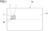
Fig. 1 is a plan view of an IC card according to a first embodiment of the present invention. -
Fig. 2 is a plan view of a rear surface side of an IC module provided to the IC card illustrated inFig. 1 . -
Fig. 3 is a cross-sectional view along line A-A illustrated inFig. 2 . -
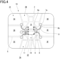
Fig. 4 is a plan view of a rear surface side of an IC module according to a second embodiment. - An IC module and a method for manufacturing an IC module according to embodiments of the present invention will be described with reference to the drawings.
- As illustrated in
Fig. 1 , anIC module 1 according to the present embodiment is used, for example, in anIC card 100 such as a credit card, a debit card, a cash card, or a card for access control. TheIC module 1 is mounted on acard body 101 of theIC card 100. - The
IC module 1 is mounted with an IC chip 10 (seeFig. 2 ) constituting an integrated circuit having both a contact communication function and a contactless communication function. TheIC module 1 has a sheet-like substrate 2 and a metal surface 3 (metal plate) that is one surface of thesubstrate 2 and covers almost the entirety of afront surface 2A (contact side). - A direction perpendicular to the
front surface 2A (first surface ) and arear surface 2B (second surface) opposite thefront surface 2A of thesubstrate 2 is referred to as a thickness direction of thesubstrate 2, and a view seen to the thickness direction is referred to as a plan view. - As illustrated in
Fig. 2 andFig. 3 , as theIC chip 10, a chip of a known configuration having a contact communication function and a contactless communication function may be used. TheIC chip 10 is formed in a rectangular shape in plan view. TheIC chip 10 is bonded to thesubstrate 2 by, for example, an adhesive agent for die attach. A plurality ofconnection terminals 11 to serve as electrodes is formed on an exposed outer surface of theIC chip 10. - Here,
Fig. 2 illustrates therear surface 2B of thesubstrate 2 in theIC module 1 and indicates themetal surface 3 and a later-describedslit 5 on thefront surface 2A by broken lines for facilitating explanation of the present embodiment. - The
substrate 2 is formed in a rectangular shape in plan view. The thickness of thesubstrate 2 is, for example, 50 to 200 µm. - On the
front surface 2A of thesubstrate 2, a terminal 31 (first terminal) for contact communication to be used for contact communication and a non-terminal metal surface 32 (second terminal) not to be used for contact communication are disposed. Therear surface 2B, which is the other surface opposite thefront surface 2A of thesubstrate 2, forms a coil-formed substrate surface having an unillustrated loop coil (hereinafter, a connection coil) for contactless communication. That is, therear surface 2B is disposed with a connection coil configured to be used for contactless communication and connected to an antenna on thecard body 101 side via a bridge circuit on thefront surface 2A. - A plurality of (here, eight) terminal regions (3A to 3H) is formed in the
metal surface 3 by disposing aslit 5, and the above-describeterminal 31 for contact communication and, in anon-terminal region 31 which does not function as theterminal 31 for contact communication, thenon-terminal metal surface 32 are formed. It is noted that a part of thenon-terminal metal surface 32 may function as a signal line. Theterminal 31 for contact communication (first terminal) and the non-terminal metal surface 32 (second terminal) may be linked directly or via a wiring pattern or the like. - The
terminal 31 for contact communication is constituted by a metal plated layer formed on thefront surface 2A of thesubstrate 2 through anadhesive material layer 4. The metal plate having themetal surface 3 is formed with a metal material having conductivity, such as nickel, palladium, gold, and copper. Theadhesive material layer 4 is provided over the entire surface of thefront surface 2A of thesubstrate 2. - The size and shape of the
IC module 1 as well as the number and positions ofterminals 31 for contact communication are defined according to a general standard of an IC module. In the present embodiment, fourterminals 31 for contact communication are provided on each of both sides sandwiching thenon-terminal metal surface 32 positioned in the left-light center on the paper ofFig. 2 in plan view. Further, the center portion on thefront surface 2A of thesubstrate 2 is thenon-terminal metal surface 32. - That is, on the
front surface 2A of thesubstrate 2, thenon-terminal metal surface 32 as themetal surface 3 is also formed in a portion other than the terminal surface (terminal surface for contact communication) used as theterminal 31 for contact communication. - Specifically, in the
IC module 1, all or a part of the eightterminal regions 3A to 3H that are sectioned by theslit 5 and positioned on both the left and right sides in themetal surface 3 is used as theterminal 31 for contact communication. Each of the eightterminals 31 for contact communication forms a substantially rectangular shape in plan view. Thenon-terminal metal surface 32 is disposed in the center portion of themetal surface 3 sectioned by theslit 5. Thenon-terminal metal surface 32 is formed in thenon-terminal region 31 having an optional planar shape. It is noted that a part of the non-terminal region 3I formed in thenon-terminal metal surface 32 may function as a signal line. Further, thenon-terminal metal surface 32 is configured to be the center region on thefront surface 2A of thesubstrate 2 surrounded by theslit 5 but is not limited to be completely surrounded by theslit 5. Thenon-terminal metal surface 32 may be disposed in a location other than the center region on thefront surface 2A. - In the
IC module 1, a connection coil for contactless communication (not illustrated) formed in a spiral shape so as to surround theIC chip 10 illustrated inFig. 2 is provided to therear surface 2B, of thesubstrate 2, constituting a coil-formed substrate surface, and contactless mutual communication between theIC module 1 and another communication machine is enabled at least via this connection coil. It is noted that the form of the connection coil is similar to that of a connection coil in a known IC module. The connection coil is formed by patterning copper foil or aluminum foil by etching and has a thickness of, for example, 5 to 50 µm. The connection coil constitutes a contactless terminal part by electromagnetic coupling with a coupling coil (antenna) of thecard body 101 illustrated inFig. 1 . - During contactless communication via the connection coil on the
rear surface 2B of thesubstrate 2, an eddy current occurs on the terminal 31 for contact communication and thenon-terminal metal surface 32. This eddy current occurs along a closed loop along the outer circumferential ends of theterminal regions 3A to 3H formed by theslit 5. An eddy current occurs in each of the sixterminal regions 3A to 3H formed by theslit 5. As the closed loop is larger, a larger eddy current occurs. - The
substrate 2 is formed mainly from an insulating substrate (insulating material) such as glass epoxy, polyimide (PI), or the like in a rectangular shape in plan view. The thickness of thesubstrate 2 is, for example, 50 to 200 µm. On therear surface 2B of thesubstrate 2, an internal wiring having abonding wire 6 is disposed. The internal wiring electrically couples the above-describedterminal 31 for contact communication to an antenna of a metal plate. - In the central part on the
rear surface 2B of thesubstrate 2 in plan view, theIC chip 10 is provided in a portion corresponding to a side opposite thenon-terminal metal surface 32 on thefront surface 2A. Around theIC chip 10, a plurality of metal plated pads 8 (connection pads) formed from metal plating is provided. Each of the plurality of metal platedpads 8 is joined to theconnection terminal 11 of theIC chip 10 by thebonding wire 6. - In the
substrate 2, a metal through hole 7 having a diameter of, for example, 0.4 to 1.0 mm and extending from the terminal 31 for contact communication on thefront surface 2A of thesubstrate 2 to therear surface 2B of thesubstrate 2 when seen from the thickness direction. It is noted that the shape of the through hole 7 illustrated inFig. 2 is circular in plan view but is not limited to being circular. A via 7a constituted by a conductive body such as metal is provided to an inner surface of the through hole 7, and the via 7a is connected to the terminal 31 for contact communication. The via 7a is formed from, for example, a metal material having conductivity such as solder, silver paste, or copper plating. The via 7a of the present embodiment is provided to the inner surface of the through hole 7 and formed in a tubular shape, but the via 7a may be formed in a columnar shape that fills the inside of the through hole 7. - In the present embodiment, the via 7a is provided in each of five regions among the eight
terminals 31 for contact communication. The via 7a is connected to the metal platedpad 8 to be connected to theIC chip 10 by thebonding wire 6. - The metal plated
pad 8 is formed in a band shape in plan view, in such a manner as to extend from a position near theIC chip 10 to the via 7a which is disposed from thenon-terminal metal surface 32 to each of theterminal regions terminals 31 for contact communication across a position, on therear surface 2B of thesubstrate 2, corresponding to theslit 5 on thefront surface 2A (across a position overlapping theslit 5 when seen in the thickness direction). That is, afirst connection end 8a as one end of the metal platedpad 8 is positioned near theIC chip 10, and asecond connection end 8b as the other end is connected to the via 7a. Thefirst connection end 8a is a bonding part to be bonded with thebonding wire 6. - It is noted that the
first connection end 8a of the present embodiment is provided to an end, of the metal platedpad 8, closer to theIC chip 10 but is not limited thereto, and thefirst connection end 8a may be provided in a location, in the metal platedpad 8, positioned closer to theIC chip 10 than to the via 7a and overlapping thenon-terminal metal surface 32 on thefront surface 2A when seen in the thickness direction. Thefirst connection end 8a is disposed in a position which does not overlap theslit 5 and overlaps thenon-terminal metal surface 32 when seen from the thickness direction. - Examples of the material of the metal plated
pad 8 include nickel, palladium, and gold (plating). The metal platedpad 8 may be formed from, for example, a conductive joining material such as solder or silver paste. - The
bonding wire 6 is, for example, a wire material such as gold or copper having a diameter of 10 to 40 µm and connects theconnection terminal 11 of theIC chip 10 and thefirst connection end 8a of the metal platedpad 8 to each other in such a manner as to step over therebetween. As the material of thebonding wire 6, for example, a gold line, a silver line, a copper line, or a line coated with other alloys or different types of metals may be adopted. - Further, the metal plated
pad 8 on therear surface 2B of thesubstrate 2 is positioned in a surrounding portion of theIC chip 10. The distance from the outer circumferential end of theIC chip 10 to thefirst connection end 8a of the metal platedpad 8 may be set to, for example, 100 µm or more and 1000 µm or less. The handling of thebonding wire 6 is optional, but the deformation amount of thebonding wire 6 caused by stress can be reduced by shortening the length of thebonding wire 6. It is noted that the outer circumferential end of theIC chip 10 is equivalent to the outer edge of theIC chip 10 when seen in the thickness direction. - Here, the
bonding wire 6 extending toward one direction of thesubstrate 2 is set to be longer than the distance between thefirst connection end 8a of the metal platedpad 8 and theconnection terminal 11 of theIC chip 10 in this one direction and is provided in a loosened state. - The length of the
bonding wire 6 may be, for example, 100 µm or more and 1000 µm or less. - To the
rear surface 2B of thesubstrate 2, unillustrated sealing resin is disposed, and theIC chip 10, the metal platedpad 8, thebonding wire 6, and the like are sealed in this sealing resin. - In the
IC module 1 configured in this manner, a circuit is formed in thesubstrate 2 by bonding, for example, copper foil on both surfaces of a glass epoxy substrate and performing an etching treatment. Thereafter, nickel, gold, palladium, or the like is laminated by a plating treatment. TheIC module 1 can be manufactured by providing the through hole 7 as necessary, forming the via 7a on the inner surface of the through hole 7 by copper plating or the like, and allowing conductor patterns on the front and rear surfaces of thesubstrate 2 to communicate with each other by the via 7a. - Next, the operation of the
IC module 1 and the method for manufacturing theIC module 1 described above will be described in detail based on the drawings. - In the present embodiment, as illustrated in
Fig. 2 and Fig. 3 , the positions of theterminal regions 3A to 3H of theterminals 31 for contact communication constituting the conductor pattern in thesubstrate 2 are determined in accordance with the terminal position dimension on the IC card 100 (seeFig. 1 ) defined in the ISO standard. Therefore, the central region on therear surface 2B of thesubstrate 2 on which theIC chip 10 is placed comes to be a region corresponding to a side opposite the non-terminal metal surface 32 (non-terminal region 3I) surrounded by theslit 5 where the conductor pattern of themetal surface 3 does not exist on thefront surface 2A. In this case, disposing the metal platedpad 8 formed on therear surface 2B of thesubstrate 2 to a position corresponding to a side opposite the central region (non-terminal metal surface 32) in the conductor pattern on thefront surface 2A produces a configuration in which thebonding wire 6 linking between theconnection terminal 11 of theIC chip 10 and the metal platedpad 8 on therear surface 2B does not step over a portion, on therear surface 2B, corresponding to a portion (slit 5) where the conductor on thefront surface 2A side does not exist. That is, thebonding wire 6 is disposed in a position not overlapping theslit 5 when seen from the thickness direction. - Since a portion without the conductor on the
front surface 2A of thesubstrate 2 is theslit 5 having a slit shape, deformation of this portion to external stress increases. Therefore, in the present embodiment, not disposing thebonding wire 6 in such a manner as to step over a portion, on therear surface 2B, corresponding to a region (slit 5) without the conductor on thefront surface 2A can reduce the external force to act on thebonding wire 6 caused by external stress and suppress a fracture risk. - Further, in the present embodiment, the position of the metal plated
pad 8 on therear surface 2B of thesubstrate 2 is the surrounding portion of theIC chip 10. For example, the distance from the outer circumferential end of theIC chip 10 to thefirst connection end 8a of the metal platedpad 8 is set to 100 µm or more and 1000 µm or less. - Since this can shorten the length of the
bonding wire 6, the external force to act on thebonding wire 6 caused by external stress can be further reduced, and a fracture risk can be suppressed. - Further, in the present embodiment, the extending direction of the
bonding wire 6 is provided in a direction along the lengthwise direction of thesubstrate 2, and thebonding wire 6 is set to be longer than the distance between thefirst connection end 8a of the metal platedpad 8 and theconnection terminal 11 of theIC chip 10 and is provided in a loosened state. - According to this configuration, for example, when external stress, which causes the IC card to be bent along a direction intersecting the extending direction of the
bonding wire 6 as the center axis of the bending in plan view, acts on theIC module 1, tensile force acts on thebonding wire 6 in the extending direction. In this case, since thebonding wire 6 is provided in a loosened state, fracture of thebonding wire 6 can be suppressed. - In this manner, in the present embodiment, external force to act on the
bonding wire 6 provided to theIC module 1 can be suppressed, and disconnection of thebonding wire 6 can be suppressed. - A conductor pattern applicable to an IC module for contact communication or for contactless communication is not necessarily the eight-terminal product of the first embodiment and may be any design (conductor pattern) on the contact side as the
front surface 2A side of thesubstrate 2. - For example,
Fig. 4 illustrates therear surface 2B of thesubstrate 2 as a six-terminal product in anIC module 1A according to the present second embodiment. - As illustrated in
Fig. 4 , theIC module 1A according to the second embodiment also has a configuration substantially equivalent to that of the above-describedIC module 1 and includes sixterminal regions 3A to 3F of theterminals 31 for contact communication constituting a conductor pattern which are disposed in thesubstrate 2. The central region on therear surface 2B of thesubstrate 2 on which theIC chip 10 is placed comes to be a region corresponding to a side opposite the non-terminal metal surface 32 (non-terminal region 3I) surrounded by theslit 5 where the conductor pattern of themetal surface 3 does not exist on thefront surface 2A. In this case, disposing the metal platedpad 8 formed on therear surface 2B of thesubstrate 2 to a position corresponding to the central region (non-terminal metal surface 32) in the conductor pattern on thefront surface 2A produces a configuration in which thebonding wire 6 linking between theconnection terminal 11 of theIC chip 10 and the metal platedpad 8 on therear surface 2B does not step over a portion (slit 5) where the conductor on thefront surface 2A side does not exist. - Subsequently, comparison results of the durability by a 3-wheel test, which was performed to a plastic card (IC card; hereinafter, may be merely referred to as a card) mounted with the
IC module 1 as the eight-terminal product described in the first embodiment or theIC module 1A as the six-terminal product described in the second embodiment, will be described. In the following Table 1, the 3-wheel test results using a plastic card mounted with six-terminal or eight-terminal IC module are illustrated. The 3-wheel test is a durability test simulating a condition in which stress acts while a card is inserted into an ATM. Specifically, when a card is inserted into an ATM, the card is held between one transfer wheel disposed on one surface and two transfer wheels disposed on the other surface, transferred by these wheels rotating, and subjected to stress by the wheels during this transfer, causing external force to be applied to the contact terminal part. When external force is repeatedly applied to the contact terminal part, for example, the bonding wire in the sealing resin may be disconnected, and communication may be disabled. For the transfer wheels, an external force of 8 N is defined as a criterion in the ISO, and external forces of 8 N, 10 N (recommended), and 12 N (recommended) are defined as a criterion in the card quality management (CQM) standard. In the following Table 1, "X/Y Passed" indicates that X test pieces out of Y test pieces have passed.[Table 1] Test condition (50 times for each of front and rear) Six-terminal product Eight-terminal product Known configuration Present configuration Known configuration Present configuration 8 N (ISO, CQM) 7/10 Passed 10/10 Passed 12/15 Passed 15/15 Passed 10 N (CQM) 8/10 Passed 10/10 Passed 11/14 Passed 15/15 Passed 12 N (CQM) 3/10 Passed 9/10 Passed 5/15 Passed 15/15 Passed - In a case of the known configuration, the result of the 3-wheel test for each of the six-terminal product and the eight-terminal product satisfied neither the ISO nor CQM standard. On the other hand, as found from the result of the 3-wheel test using the IC module having the configuration of the present application, the six-terminal product and the eight-terminal product both improved in durability. In the known configuration, the connection end of the connection pad (i.e., the metal plated pad 8) is positioned in a portion, on the rear surface, corresponding to the slit on the front surface, so that deformation of the connection pad to external stress is large, causing an increase in external force to act on the 2nd bonding part (the bonding portion of the bonding wire on the connection pad). It is considered that this caused the disconnection of the bonding wire and the occurrence of communication failure.
- For the IC module having the known configuration and the IC module having the configuration of the present application, the lengths of the bonding wires are compared, and the result is illustrated in the following Table 2. It is understood that since the connection pad in the IC module having the configuration of the present application is located near the IC chip as compared to the known configuration, the average length of the bonding wire having the configuration of the present application is less than half that of the known configuration. Further, in the IC module having the present configuration, unlike in the product having the known configuration, the bonding pad (2nd bonding part) is not disposed in a position, on the rear surface, stepping over a portion corresponding to the slit provided between the plurality of terminals on the front surface, and therefore, external force to act on the bonding part in response to application with external stress is reduced.
[Table 2] Eight-terminal module/mm Six-terminal module/mm Known configuration Present configuration Known configuration Present configuration Type of terminal GND 1.0 0.7 2.3 0.6 I/O 1.0 0.6 1.7 0.6 VCC 1.0 0.6 2.3 0.7 RST 1.1 0.7 1.6 0.7 CLK 1.3 0.8 1.8 0.5 ACO 1.4 0.5 0.9 0.8 AC1 1.2 0.5 1.0 0.7 Maximum 1.4 0.8 2.3 0.8 Minimum 1.0 0.5 0.9 0.5 Average 1.2 0.6 1.7 0.7 - As described above, the IC modules 1 and 1A of the above-described embodiments each includes: a substrate 2 that has a front surface 2A (first surface) and a rear surface 2B (second surface) opposite the front surface 2A and has a metal surface 3 at least on the front surface 2A; and an IC chip 10 that has both a contact communication function and a contactless communication function and is mounted on the rear surface 2B of the substrate 2, in which a plurality of terminals constituted by the metal surface 3 is formed on the front surface 2A of the substrate 2, the plurality of terminals containing a terminal 31 for contact communication (first terminal) used for contact communication and a non-terminal metal surface 32 (second terminal) other than the terminal 31 for contact communication, and the substrate 2 includes a via 7a that is formed on an inner surface of a through hole 7 penetrating from the front surface 2A to the rear surface 2B and is connected to the terminal 31 for contact communication, a metal plated pad 8 (connection pad), made of metal, extending from the via 7a to a portion, on the rear surface 2B, positioned opposite the non-terminal metal surface 32 overlapping the IC chip 10 when seen from a thickness direction of the substrate 2, and a bonding wire 6 that connects between a first connection end 8a (connection end), of the metal plated pad 8, positioned closer to the IC chip 10 than to the via 7a and a connection terminal 11 of the IC chip 10.
- In the
IC modules substrate 2 has aslit 5 between the plurality of terminals such as the terminal 31 for contact communication and thenon-terminal metal surface 32, and thebonding wire 6 is disposed in a position not overlapping theslit 5 when seen in the thickness direction. - In the
IC modules IC chip 10 on therear surface 2B (second surface) of thesubstrate 2. - In the
IC modules IC chip 10 to thefirst connection end 8a (connection end) of the metal plated pad 8 (connection pad) is, for example, 1000 µm or less. - In the
IC modules - In the
IC modules bonding wire 6 extending toward one direction of thesubstrate 2 is set to be longer than the distance between thefirst connection end 8a (connection end) of the metal plated pad 8 (connection pad) and theconnection terminal 11 of theIC chip 10 in the one direction and is provided in a loosened state. - The method for manufacturing an IC module including a substrate 2 that has a front surface 2A (first surface) and a rear surface 2B (second surface) opposite the front surface 2A and has a metal surface 3 at least on the front surface 2A and an IC chip 10 that has both a contact communication function and a contactless communication function and is mounted on the rear surface 2B of the substrate 2, according to the above-described embodiment, includes: forming, on the front surface 2A of the substrate 2, a plurality of terminals that is constituted by the metal surface 3 and contains a terminal 31 for contact communication (first terminal) used for contact communication and a non-terminal metal surface 32 (second terminal) other than the terminal 31 for contact communication; providing, on an inner surface of a through hole 7 penetrating from the front surface 2A to the rear surface 2B, a via 7a connected to the terminal 31 for contact communication; providing a metal plated pad 8 (connection pad) extending from the via 7a to a portion, on the rear surface 2B, positioned opposite the non-terminal metal surface 32 overlapping the IC chip 10 when seen from the thickness direction of the substrate 2; and connecting between the first connection end 8a (connection end), of the metal plated pad 8, positioned closer to the IC chip 10 than to the via 7a and the connection terminal 11 of the IC chip 10 by a bonding wire 6.
- The embodiments of the present invention have been described above in detail with reference to the drawings, but specific configurations are not limited to the embodiments and also encompass modifications, combinations, and the like of the configurations within the scope of the present invention.
- For example, the position of the metal plated
pad 8 on therear surface 2B of thesubstrate 2 is configured to be the surrounding portion of theIC chip 10 in the present embodiment, but it is enough for thefirst connection end 8a of the metal platedpad 8 to be in a portion overlapping the non-terminal metal surface 32 (non-terminal region 3I) on thefront surface 2A, and the metal platedpad 8 may not be provided in the surrounding portion of theIC chip 10. - Further, an example in which the distance from the end of the
IC chip 10 to thefirst connection end 8a of the metal platedpad 8 is 100 µm or more and 1000 µm or less has been illustrated, but the distance may be outside this range. - An example in which the length of the
bonding wire 6 is 100 µm or more and 1000 µm or less has been illustrated, but the length may be outside this range. - Furthermore, the present embodiment has a configuration in which the extending direction of the
bonding wire 6 is provided in a direction along the lengthwise direction of thesubstrate 2, and thebonding wire 6 is set to be longer than the distance between thefirst connection end 8a of the metal platedpad 8 and theconnection terminal 11 of theIC chip 10 and is provided in a loosened state. However, the configuration is not limited to disposing thebonding wire 6 in a loosened state in this manner, and thebonding wire 6 may have the same length as the distance between thefirst connection end 8a of the metal platedpad 8 and theconnection terminal 11 of theIC chip 10. - The
non-terminal metal surface 32 of the present embodiment is not used for contact communication but is not limited thereto, and thenon-terminal metal surface 32 may be, for example, a terminal used for contact communication in an operation test of the IC module. -
- 100: IC card
- 1, 1A: IC module
- 2: Substrate
- 2A: Front surface
- 2B: Rear surface
- 3: Metal surface
- 3A to 3H: Terminal region
- 3I: Non-terminal region
- 4: Adhesive material layer
- 5: Slit
- 6: Bonding wire
- 7: Through hole
- 7A: Via
- 8: Metal plated pad (connection pad)
- 8A: First connection end
- 10: IC chip
- 11: Connection terminal
- 31: Terminal for contact communication (first terminal)
- 32: Non-terminal metal surface (second terminal)
Claims (7)
- An IC module comprising: a substrate that has a first surface and a second surface opposite the first surface and has a metal surface at lease on the first surface; and an IC chip that has both a contact communication function and a contactless communication function and is mounted on the second surface of the substrate, whereina plurality of terminals constituted by the metal surface is formed on the first surface of the substrate, the plurality of terminals containing a first terminal used for contact communication and a second terminal other than the first terminal, andthe substrate includesa via that is formed on an inner surface of a through hole penetrating from the first surface to the second surface and is connected to the first terminal,a metal connection pad extending from the via to a portion, on the second surface, positioned opposite the second terminal overlapping the IC chip when seen from a thickness direction of the substrate, anda bonding wire that connects between a connection end, of the connection pad, positioned closer to the IC chip than to the via and a connection terminal of the IC chip.
- The IC module according to claim 1, whereinthe substrate has a slit between the plurality of terminals, andthe bonding wire is disposed in a position that does not overlap the slit when seen from the thickness direction.
- The IC module according to claim 1, wherein the connection pad is positioned in a surrounding portion of the IC chip on the second surface of the substrate.
- The IC module according to claim 3, wherein a distance from an outer circumferential end of the IC chip to the connection end of the connection pad is 1000 µm or less.
- The IC module according to claim 4, wherein a length of the bonding wire is 1000 µm or less.
- The IC module according to any one of claims 1 to 5, wherein the bonding wire extending toward one direction of the substrate is set to be longer than a distance between the connection end of the connection pad and the connection terminal of the IC chip in the one direction and is provided in a loosened state.
- A method for manufacturing an IC module including a substrate that has a first surface and a second surface opposite the first surface and has a metal surface at lease on the first surface and an IC chip that has both a contact communication function and a contactless communication function and is mounted on the second surface of the substrate, comprising:forming, on the first surface of the substrate, a plurality of terminals that is constituted by the metal surface and contains a first terminal used for connection communication and a second terminal other than the first terminal;providing, on an inner surface of a through hole penetrating from the first surface to the second surface, a via connected to the first terminal;providing a metal connection pad extending from the via to a portion, on the second surface, positioned opposite the second terminal overlapping the IC chip when seen from a thickness direction of the substrate; andconnecting between a connection end, of the connection pad, positioned closer to the IC chip than to the via and a connection terminal of the IC chip by a bonding wire.
Applications Claiming Priority (2)
| Application Number | Priority Date | Filing Date | Title |
|---|---|---|---|
| JP2021182372 | 2021-11-09 | ||
| PCT/JP2022/041696 WO2023085312A1 (en) | 2021-11-09 | 2022-11-09 | Ic module and method for manufacturing ic module |
Publications (3)
| Publication Number | Publication Date |
|---|---|
| EP4432159A1 true EP4432159A1 (en) | 2024-09-18 |
| EP4432159A4 EP4432159A4 (en) | 2025-03-05 |
| EP4432159B1 EP4432159B1 (en) | 2026-04-29 |
Family
ID=86335797
Family Applications (1)
| Application Number | Title | Priority Date | Filing Date |
|---|---|---|---|
| EP22892810.7A Active EP4432159B1 (en) | 2021-11-09 | 2022-11-09 | Ic module and method for manufacturing ic module |
Country Status (5)
| Country | Link |
|---|---|
| US (1) | US20240290747A1 (en) |
| EP (1) | EP4432159B1 (en) |
| JP (1) | JPWO2023085312A1 (en) |
| CN (1) | CN118043817A (en) |
| WO (1) | WO2023085312A1 (en) |
Family Cites Families (3)
| Publication number | Priority date | Publication date | Assignee | Title |
|---|---|---|---|---|
| JPH04182198A (en) * | 1990-11-16 | 1992-06-29 | Dainippon Printing Co Ltd | Ic module and ic card |
| JP5445300B2 (en) * | 2010-04-15 | 2014-03-19 | 大日本印刷株式会社 | IC module and IC card |
| JP2021182372A (en) | 2020-04-13 | 2021-11-25 | 株式会社Anamorphosis Networks | Program providing method, program providing device, and computer program |
-
2022
- 2022-11-09 EP EP22892810.7A patent/EP4432159B1/en active Active
- 2022-11-09 JP JP2023559668A patent/JPWO2023085312A1/ja active Pending
- 2022-11-09 WO PCT/JP2022/041696 patent/WO2023085312A1/en not_active Ceased
- 2022-11-09 CN CN202280066608.7A patent/CN118043817A/en active Pending
-
2024
- 2024-05-07 US US18/657,067 patent/US20240290747A1/en active Pending
Also Published As
| Publication number | Publication date |
|---|---|
| EP4432159A4 (en) | 2025-03-05 |
| JPWO2023085312A1 (en) | 2023-05-19 |
| WO2023085312A1 (en) | 2023-05-19 |
| CN118043817A (en) | 2024-05-14 |
| EP4432159B1 (en) | 2026-04-29 |
| US20240290747A1 (en) | 2024-08-29 |
Similar Documents
| Publication | Publication Date | Title |
|---|---|---|
| CN1881241B (en) | Non-contact data carrier and method of fabricating the same | |
| US10679117B2 (en) | Dual IC card | |
| US6208019B1 (en) | Ultra-thin card-type semiconductor device having an embredded semiconductor element in a space provided therein | |
| CN101156164B (en) | Noncontact information storage medium and method for manufacturing same | |
| CN108878407A (en) | Semiconductor package device and method of manufacturing the same | |
| CN115552410B (en) | Card media | |
| CN104995642A (en) | Simplified electronic module for a smart card with a dual communication interface | |
| US6469371B2 (en) | Non-contact type IC card and process for manufacturing same | |
| US5917235A (en) | Semiconductor device having LOC structure, a semiconductor device lead frame, TAB leads, and an insulating TAB tape | |
| AU2023433488B2 (en) | Articles of manufacture relating to ic modules and smart cards | |
| JP2009031956A (en) | Contact / non-contact common type IC card and method of manufacturing contact / non-contact common type IC card | |
| JP2014178731A (en) | Method for manufacturing semiconductor device | |
| JP5344000B2 (en) | IC module and IC card for both contact and non-contact | |
| EP4432159B1 (en) | Ic module and method for manufacturing ic module | |
| EP3688668B1 (en) | Strap mounting techniques for wire format antennas | |
| JP3877988B2 (en) | Semiconductor device | |
| JP2002536733A (en) | Integrated circuit device, electronic unit for smart card using the device, and method of manufacturing the device | |
| JP2002207982A (en) | Contactless and non-contact IC module and IC card | |
| JP4736557B2 (en) | IC module for IC card and manufacturing method thereof | |
| US6396132B1 (en) | Semiconductor device with improved interconnections between the chip and the terminals, and process for its manufacture | |
| KR20210060476A (en) | Method for manufacturing an electronic module for a portable object | |
| JP3567617B2 (en) | Semiconductor device using TAB tape | |
| HK40119002B (en) | Articles of manufacture relating to ic modules and smart cards | |
| HK40119002A (en) | Articles of manufacture relating to ic modules and smart cards | |
| JP2024059157A (en) | IC module sheet, electromagnetic coupling type IC module, and dual IC card |
Legal Events
| Date | Code | Title | Description |
|---|---|---|---|
| STAA | Information on the status of an ep patent application or granted ep patent |
Free format text: STATUS: THE INTERNATIONAL PUBLICATION HAS BEEN MADE |
|
| PUAI | Public reference made under article 153(3) epc to a published international application that has entered the european phase |
Free format text: ORIGINAL CODE: 0009012 |
|
| STAA | Information on the status of an ep patent application or granted ep patent |
Free format text: STATUS: REQUEST FOR EXAMINATION WAS MADE |
|
| 17P | Request for examination filed |
Effective date: 20240515 |
|
| AK | Designated contracting states |
Kind code of ref document: A1 Designated state(s): AL AT BE BG CH CY CZ DE DK EE ES FI FR GB GR HR HU IE IS IT LI LT LU LV MC ME MK MT NL NO PL PT RO RS SE SI SK SM TR |
|
| DAV | Request for validation of the european patent (deleted) | ||
| DAX | Request for extension of the european patent (deleted) | ||
| A4 | Supplementary search report drawn up and despatched |
Effective date: 20250131 |
|
| RIC1 | Information provided on ipc code assigned before grant |
Ipc: H01L 23/00 20060101ALI20250127BHEP Ipc: H01L 23/12 20060101ALI20250127BHEP Ipc: H01L 21/60 20060101ALI20250127BHEP Ipc: G06K 19/077 20060101AFI20250127BHEP |
|
| STAA | Information on the status of an ep patent application or granted ep patent |
Free format text: STATUS: EXAMINATION IS IN PROGRESS |
|
| 17Q | First examination report despatched |
Effective date: 20250724 |
|
| GRAP | Despatch of communication of intention to grant a patent |
Free format text: ORIGINAL CODE: EPIDOSNIGR1 |
|
| STAA | Information on the status of an ep patent application or granted ep patent |
Free format text: STATUS: GRANT OF PATENT IS INTENDED |
|
| INTG | Intention to grant announced |
Effective date: 20260105 |
|
| GRAS | Grant fee paid |
Free format text: ORIGINAL CODE: EPIDOSNIGR3 |
|
| GRAA | (expected) grant |
Free format text: ORIGINAL CODE: 0009210 |
|
| STAA | Information on the status of an ep patent application or granted ep patent |
Free format text: STATUS: THE PATENT HAS BEEN GRANTED |
|
| AK | Designated contracting states |
Kind code of ref document: B1 Designated state(s): AL AT BE BG CH CY CZ DE DK EE ES FI FR GB GR HR HU IE IS IT LI LT LU LV MC ME MK MT NL NO PL PT RO RS SE SI SK SM TR |
|
| REG | Reference to a national code |
Ref country code: CH Ref legal event code: F10 Free format text: ST27 STATUS EVENT CODE: U-0-0-F10-F00 (AS PROVIDED BY THE NATIONAL OFFICE) Effective date: 20260429 Ref country code: GB Ref legal event code: FG4D |
|
| REG | Reference to a national code |
Ref country code: DE Ref legal event code: R096 Ref document number: 602022035882 Country of ref document: DE |
|
| REG | Reference to a national code |
Ref country code: IE Ref legal event code: FG4D |