EP4428913A2 - Semiconductor package having improved thermal interface between semiconductor die and heat spreading structure - Google Patents
Semiconductor package having improved thermal interface between semiconductor die and heat spreading structure Download PDFInfo
- Publication number
- EP4428913A2 EP4428913A2 EP24191249.2A EP24191249A EP4428913A2 EP 4428913 A2 EP4428913 A2 EP 4428913A2 EP 24191249 A EP24191249 A EP 24191249A EP 4428913 A2 EP4428913 A2 EP 4428913A2
- Authority
- EP
- European Patent Office
- Prior art keywords
- die
- semiconductor
- semiconductor package
- chip
- package
- Prior art date
- Legal status (The legal status is an assumption and is not a legal conclusion. Google has not performed a legal analysis and makes no representation as to the accuracy of the status listed.)
- Pending
Links
Images




Classifications
-
- H—ELECTRICITY
- H10—SEMICONDUCTOR DEVICES; ELECTRIC SOLID-STATE DEVICES NOT OTHERWISE PROVIDED FOR
- H10W—GENERIC PACKAGES, INTERCONNECTIONS, CONNECTORS OR OTHER CONSTRUCTIONAL DETAILS OF DEVICES COVERED BY CLASS H10
- H10W90/00—Package configurations
- H10W90/701—Package configurations characterised by the relative positions of pads or connectors relative to package parts
-
- H—ELECTRICITY
- H05—ELECTRIC TECHNIQUES NOT OTHERWISE PROVIDED FOR
- H05K—PRINTED CIRCUITS; CASINGS OR CONSTRUCTIONAL DETAILS OF ELECTRIC APPARATUS; MANUFACTURE OF ASSEMBLAGES OF ELECTRICAL COMPONENTS
- H05K1/00—Printed circuits
- H05K1/02—Details
- H05K1/0201—Thermal arrangements, e.g. for cooling, heating or preventing overheating
- H05K1/0203—Cooling of mounted components
- H05K1/0204—Cooling of mounted components using means for thermal conduction connection in the thickness direction of the substrate
-
- H—ELECTRICITY
- H01—ELECTRIC ELEMENTS
- H01Q—ANTENNAS, i.e. RADIO AERIALS
- H01Q1/00—Details of, or arrangements associated with, antennas
- H01Q1/02—Arrangements for de-icing; Arrangements for drying-out ; Arrangements for cooling; Arrangements for preventing corrosion
-
- H—ELECTRICITY
- H01—ELECTRIC ELEMENTS
- H01Q—ANTENNAS, i.e. RADIO AERIALS
- H01Q1/00—Details of, or arrangements associated with, antennas
- H01Q1/12—Supports; Mounting means
- H01Q1/22—Supports; Mounting means by structural association with other equipment or articles
- H01Q1/2283—Supports; Mounting means by structural association with other equipment or articles mounted in or on the surface of a semiconductor substrate as a chip-type antenna or integrated with other components into an IC package
-
- H—ELECTRICITY
- H05—ELECTRIC TECHNIQUES NOT OTHERWISE PROVIDED FOR
- H05K—PRINTED CIRCUITS; CASINGS OR CONSTRUCTIONAL DETAILS OF ELECTRIC APPARATUS; MANUFACTURE OF ASSEMBLAGES OF ELECTRICAL COMPONENTS
- H05K1/00—Printed circuits
- H05K1/18—Printed circuits structurally associated with non-printed electric components
-
- H—ELECTRICITY
- H10—SEMICONDUCTOR DEVICES; ELECTRIC SOLID-STATE DEVICES NOT OTHERWISE PROVIDED FOR
- H10W—GENERIC PACKAGES, INTERCONNECTIONS, CONNECTORS OR OTHER CONSTRUCTIONAL DETAILS OF DEVICES COVERED BY CLASS H10
- H10W20/00—Interconnections in chips, wafers or substrates
- H10W20/40—Interconnections external to wafers or substrates, e.g. back-end-of-line [BEOL] metallisations or vias connecting to gate electrodes
-
- H—ELECTRICITY
- H10—SEMICONDUCTOR DEVICES; ELECTRIC SOLID-STATE DEVICES NOT OTHERWISE PROVIDED FOR
- H10W—GENERIC PACKAGES, INTERCONNECTIONS, CONNECTORS OR OTHER CONSTRUCTIONAL DETAILS OF DEVICES COVERED BY CLASS H10
- H10W40/00—Arrangements for thermal protection or thermal control
- H10W40/20—Arrangements for cooling
- H10W40/22—Arrangements for cooling characterised by their shape, e.g. having conical or cylindrical projections
- H10W40/226—Arrangements for cooling characterised by their shape, e.g. having conical or cylindrical projections characterised by projecting parts, e.g. fins to increase surface area
-
- H—ELECTRICITY
- H10—SEMICONDUCTOR DEVICES; ELECTRIC SOLID-STATE DEVICES NOT OTHERWISE PROVIDED FOR
- H10W—GENERIC PACKAGES, INTERCONNECTIONS, CONNECTORS OR OTHER CONSTRUCTIONAL DETAILS OF DEVICES COVERED BY CLASS H10
- H10W40/00—Arrangements for thermal protection or thermal control
- H10W40/20—Arrangements for cooling
- H10W40/22—Arrangements for cooling characterised by their shape, e.g. having conical or cylindrical projections
- H10W40/226—Arrangements for cooling characterised by their shape, e.g. having conical or cylindrical projections characterised by projecting parts, e.g. fins to increase surface area
- H10W40/228—Arrangements for cooling characterised by their shape, e.g. having conical or cylindrical projections characterised by projecting parts, e.g. fins to increase surface area the projecting parts being wire-shaped or pin-shaped
-
- H—ELECTRICITY
- H10—SEMICONDUCTOR DEVICES; ELECTRIC SOLID-STATE DEVICES NOT OTHERWISE PROVIDED FOR
- H10W—GENERIC PACKAGES, INTERCONNECTIONS, CONNECTORS OR OTHER CONSTRUCTIONAL DETAILS OF DEVICES COVERED BY CLASS H10
- H10W40/00—Arrangements for thermal protection or thermal control
- H10W40/20—Arrangements for cooling
- H10W40/25—Arrangements for cooling characterised by their materials
- H10W40/257—Arrangements for cooling characterised by their materials having a heterogeneous or anisotropic structure, e.g. powder or fibres in a matrix, wire mesh or porous structures
-
- H—ELECTRICITY
- H10—SEMICONDUCTOR DEVICES; ELECTRIC SOLID-STATE DEVICES NOT OTHERWISE PROVIDED FOR
- H10W—GENERIC PACKAGES, INTERCONNECTIONS, CONNECTORS OR OTHER CONSTRUCTIONAL DETAILS OF DEVICES COVERED BY CLASS H10
- H10W40/00—Arrangements for thermal protection or thermal control
- H10W40/70—Fillings or auxiliary members in containers or in encapsulations for thermal protection or control
- H10W40/77—Auxiliary members characterised by their shape
- H10W40/778—Auxiliary members characterised by their shape in encapsulations
-
- H—ELECTRICITY
- H10—SEMICONDUCTOR DEVICES; ELECTRIC SOLID-STATE DEVICES NOT OTHERWISE PROVIDED FOR
- H10W—GENERIC PACKAGES, INTERCONNECTIONS, CONNECTORS OR OTHER CONSTRUCTIONAL DETAILS OF DEVICES COVERED BY CLASS H10
- H10W44/00—Electrical arrangements for controlling or matching impedance
- H10W44/20—Electrical arrangements for controlling or matching impedance at high-frequency [HF] or radio frequency [RF]
-
- H—ELECTRICITY
- H10—SEMICONDUCTOR DEVICES; ELECTRIC SOLID-STATE DEVICES NOT OTHERWISE PROVIDED FOR
- H10W—GENERIC PACKAGES, INTERCONNECTIONS, CONNECTORS OR OTHER CONSTRUCTIONAL DETAILS OF DEVICES COVERED BY CLASS H10
- H10W70/00—Package substrates; Interposers; Redistribution layers [RDL]
- H10W70/60—Insulating or insulated package substrates; Interposers; Redistribution layers
- H10W70/62—Insulating or insulated package substrates; Interposers; Redistribution layers characterised by their interconnections
- H10W70/65—Shapes or dispositions of interconnections
-
- H—ELECTRICITY
- H10—SEMICONDUCTOR DEVICES; ELECTRIC SOLID-STATE DEVICES NOT OTHERWISE PROVIDED FOR
- H10W—GENERIC PACKAGES, INTERCONNECTIONS, CONNECTORS OR OTHER CONSTRUCTIONAL DETAILS OF DEVICES COVERED BY CLASS H10
- H10W70/00—Package substrates; Interposers; Redistribution layers [RDL]
- H10W70/60—Insulating or insulated package substrates; Interposers; Redistribution layers
- H10W70/67—Insulating or insulated package substrates; Interposers; Redistribution layers characterised by their insulating layers or insulating parts
- H10W70/68—Shapes or dispositions thereof
- H10W70/685—Shapes or dispositions thereof comprising multiple insulating layers
-
- H—ELECTRICITY
- H10—SEMICONDUCTOR DEVICES; ELECTRIC SOLID-STATE DEVICES NOT OTHERWISE PROVIDED FOR
- H10W—GENERIC PACKAGES, INTERCONNECTIONS, CONNECTORS OR OTHER CONSTRUCTIONAL DETAILS OF DEVICES COVERED BY CLASS H10
- H10W90/00—Package configurations
-
- H—ELECTRICITY
- H10—SEMICONDUCTOR DEVICES; ELECTRIC SOLID-STATE DEVICES NOT OTHERWISE PROVIDED FOR
- H10W—GENERIC PACKAGES, INTERCONNECTIONS, CONNECTORS OR OTHER CONSTRUCTIONAL DETAILS OF DEVICES COVERED BY CLASS H10
- H10W44/00—Electrical arrangements for controlling or matching impedance
- H10W44/20—Electrical arrangements for controlling or matching impedance at high-frequency [HF] or radio frequency [RF]
- H10W44/241—Electrical arrangements for controlling or matching impedance at high-frequency [HF] or radio frequency [RF] for passive devices or passive elements
- H10W44/248—Electrical arrangements for controlling or matching impedance at high-frequency [HF] or radio frequency [RF] for passive devices or passive elements for antennas
-
- H—ELECTRICITY
- H10—SEMICONDUCTOR DEVICES; ELECTRIC SOLID-STATE DEVICES NOT OTHERWISE PROVIDED FOR
- H10W—GENERIC PACKAGES, INTERCONNECTIONS, CONNECTORS OR OTHER CONSTRUCTIONAL DETAILS OF DEVICES COVERED BY CLASS H10
- H10W72/00—Interconnections or connectors in packages
- H10W72/071—Connecting or disconnecting
- H10W72/072—Connecting or disconnecting of bump connectors
-
- H—ELECTRICITY
- H10—SEMICONDUCTOR DEVICES; ELECTRIC SOLID-STATE DEVICES NOT OTHERWISE PROVIDED FOR
- H10W—GENERIC PACKAGES, INTERCONNECTIONS, CONNECTORS OR OTHER CONSTRUCTIONAL DETAILS OF DEVICES COVERED BY CLASS H10
- H10W72/00—Interconnections or connectors in packages
- H10W72/071—Connecting or disconnecting
- H10W72/073—Connecting or disconnecting of die-attach connectors
-
- H—ELECTRICITY
- H10—SEMICONDUCTOR DEVICES; ELECTRIC SOLID-STATE DEVICES NOT OTHERWISE PROVIDED FOR
- H10W—GENERIC PACKAGES, INTERCONNECTIONS, CONNECTORS OR OTHER CONSTRUCTIONAL DETAILS OF DEVICES COVERED BY CLASS H10
- H10W72/00—Interconnections or connectors in packages
- H10W72/071—Connecting or disconnecting
- H10W72/073—Connecting or disconnecting of die-attach connectors
- H10W72/07331—Connecting techniques
- H10W72/07336—Soldering or alloying
-
- H—ELECTRICITY
- H10—SEMICONDUCTOR DEVICES; ELECTRIC SOLID-STATE DEVICES NOT OTHERWISE PROVIDED FOR
- H10W—GENERIC PACKAGES, INTERCONNECTIONS, CONNECTORS OR OTHER CONSTRUCTIONAL DETAILS OF DEVICES COVERED BY CLASS H10
- H10W72/00—Interconnections or connectors in packages
- H10W72/071—Connecting or disconnecting
- H10W72/073—Connecting or disconnecting of die-attach connectors
- H10W72/07351—Connecting or disconnecting of die-attach connectors characterised by changes in properties of the die-attach connectors during connecting
- H10W72/07352—Connecting or disconnecting of die-attach connectors characterised by changes in properties of the die-attach connectors during connecting changes in structures or sizes
-
- H—ELECTRICITY
- H10—SEMICONDUCTOR DEVICES; ELECTRIC SOLID-STATE DEVICES NOT OTHERWISE PROVIDED FOR
- H10W—GENERIC PACKAGES, INTERCONNECTIONS, CONNECTORS OR OTHER CONSTRUCTIONAL DETAILS OF DEVICES COVERED BY CLASS H10
- H10W72/00—Interconnections or connectors in packages
- H10W72/071—Connecting or disconnecting
- H10W72/073—Connecting or disconnecting of die-attach connectors
- H10W72/07351—Connecting or disconnecting of die-attach connectors characterised by changes in properties of the die-attach connectors during connecting
- H10W72/07354—Connecting or disconnecting of die-attach connectors characterised by changes in properties of the die-attach connectors during connecting changes in dispositions
-
- H—ELECTRICITY
- H10—SEMICONDUCTOR DEVICES; ELECTRIC SOLID-STATE DEVICES NOT OTHERWISE PROVIDED FOR
- H10W—GENERIC PACKAGES, INTERCONNECTIONS, CONNECTORS OR OTHER CONSTRUCTIONAL DETAILS OF DEVICES COVERED BY CLASS H10
- H10W72/00—Interconnections or connectors in packages
- H10W72/20—Bump connectors, e.g. solder bumps or copper pillars; Dummy bumps; Thermal bumps
- H10W72/251—Materials
- H10W72/252—Materials comprising solid metals or solid metalloids, e.g. PbSn, Ag or Cu
-
- H—ELECTRICITY
- H10—SEMICONDUCTOR DEVICES; ELECTRIC SOLID-STATE DEVICES NOT OTHERWISE PROVIDED FOR
- H10W—GENERIC PACKAGES, INTERCONNECTIONS, CONNECTORS OR OTHER CONSTRUCTIONAL DETAILS OF DEVICES COVERED BY CLASS H10
- H10W72/00—Interconnections or connectors in packages
- H10W72/30—Die-attach connectors
- H10W72/321—Structures or relative sizes of die-attach connectors
-
- H—ELECTRICITY
- H10—SEMICONDUCTOR DEVICES; ELECTRIC SOLID-STATE DEVICES NOT OTHERWISE PROVIDED FOR
- H10W—GENERIC PACKAGES, INTERCONNECTIONS, CONNECTORS OR OTHER CONSTRUCTIONAL DETAILS OF DEVICES COVERED BY CLASS H10
- H10W72/00—Interconnections or connectors in packages
- H10W72/30—Die-attach connectors
- H10W72/341—Dispositions of die-attach connectors, e.g. layouts
- H10W72/347—Dispositions of multiple die-attach connectors
-
- H—ELECTRICITY
- H10—SEMICONDUCTOR DEVICES; ELECTRIC SOLID-STATE DEVICES NOT OTHERWISE PROVIDED FOR
- H10W—GENERIC PACKAGES, INTERCONNECTIONS, CONNECTORS OR OTHER CONSTRUCTIONAL DETAILS OF DEVICES COVERED BY CLASS H10
- H10W72/00—Interconnections or connectors in packages
- H10W72/30—Die-attach connectors
- H10W72/351—Materials of die-attach connectors
- H10W72/353—Materials of die-attach connectors not comprising solid metals or solid metalloids, e.g. ceramics
- H10W72/354—Materials of die-attach connectors not comprising solid metals or solid metalloids, e.g. ceramics comprising polymers
-
- H—ELECTRICITY
- H10—SEMICONDUCTOR DEVICES; ELECTRIC SOLID-STATE DEVICES NOT OTHERWISE PROVIDED FOR
- H10W—GENERIC PACKAGES, INTERCONNECTIONS, CONNECTORS OR OTHER CONSTRUCTIONAL DETAILS OF DEVICES COVERED BY CLASS H10
- H10W72/00—Interconnections or connectors in packages
- H10W72/851—Dispositions of multiple connectors or interconnections
- H10W72/853—On the same surface
- H10W72/865—Die-attach connectors and bond wires
-
- H—ELECTRICITY
- H10—SEMICONDUCTOR DEVICES; ELECTRIC SOLID-STATE DEVICES NOT OTHERWISE PROVIDED FOR
- H10W—GENERIC PACKAGES, INTERCONNECTIONS, CONNECTORS OR OTHER CONSTRUCTIONAL DETAILS OF DEVICES COVERED BY CLASS H10
- H10W72/00—Interconnections or connectors in packages
- H10W72/851—Dispositions of multiple connectors or interconnections
- H10W72/874—On different surfaces
- H10W72/877—Bump connectors and die-attach connectors
-
- H—ELECTRICITY
- H10—SEMICONDUCTOR DEVICES; ELECTRIC SOLID-STATE DEVICES NOT OTHERWISE PROVIDED FOR
- H10W—GENERIC PACKAGES, INTERCONNECTIONS, CONNECTORS OR OTHER CONSTRUCTIONAL DETAILS OF DEVICES COVERED BY CLASS H10
- H10W72/00—Interconnections or connectors in packages
- H10W72/851—Dispositions of multiple connectors or interconnections
- H10W72/874—On different surfaces
- H10W72/884—Die-attach connectors and bond wires
-
- H—ELECTRICITY
- H10—SEMICONDUCTOR DEVICES; ELECTRIC SOLID-STATE DEVICES NOT OTHERWISE PROVIDED FOR
- H10W—GENERIC PACKAGES, INTERCONNECTIONS, CONNECTORS OR OTHER CONSTRUCTIONAL DETAILS OF DEVICES COVERED BY CLASS H10
- H10W74/00—Encapsulations, e.g. protective coatings
- H10W74/10—Encapsulations, e.g. protective coatings characterised by their shape or disposition
- H10W74/111—Encapsulations, e.g. protective coatings characterised by their shape or disposition the semiconductor body being completely enclosed
- H10W74/114—Encapsulations, e.g. protective coatings characterised by their shape or disposition the semiconductor body being completely enclosed by a substrate and the encapsulations
- H10W74/117—Encapsulations, e.g. protective coatings characterised by their shape or disposition the semiconductor body being completely enclosed by a substrate and the encapsulations the substrate having spherical bumps for external connection
-
- H—ELECTRICITY
- H10—SEMICONDUCTOR DEVICES; ELECTRIC SOLID-STATE DEVICES NOT OTHERWISE PROVIDED FOR
- H10W—GENERIC PACKAGES, INTERCONNECTIONS, CONNECTORS OR OTHER CONSTRUCTIONAL DETAILS OF DEVICES COVERED BY CLASS H10
- H10W74/00—Encapsulations, e.g. protective coatings
- H10W74/10—Encapsulations, e.g. protective coatings characterised by their shape or disposition
- H10W74/131—Encapsulations, e.g. protective coatings characterised by their shape or disposition the semiconductor body being only partially enclosed
- H10W74/142—Encapsulations, e.g. protective coatings characterised by their shape or disposition the semiconductor body being only partially enclosed the encapsulations exposing the passive side of the semiconductor body
-
- H—ELECTRICITY
- H10—SEMICONDUCTOR DEVICES; ELECTRIC SOLID-STATE DEVICES NOT OTHERWISE PROVIDED FOR
- H10W—GENERIC PACKAGES, INTERCONNECTIONS, CONNECTORS OR OTHER CONSTRUCTIONAL DETAILS OF DEVICES COVERED BY CLASS H10
- H10W74/00—Encapsulations, e.g. protective coatings
- H10W74/10—Encapsulations, e.g. protective coatings characterised by their shape or disposition
- H10W74/15—Encapsulations, e.g. protective coatings characterised by their shape or disposition on active surfaces of flip-chip devices, e.g. underfills
-
- H—ELECTRICITY
- H10—SEMICONDUCTOR DEVICES; ELECTRIC SOLID-STATE DEVICES NOT OTHERWISE PROVIDED FOR
- H10W—GENERIC PACKAGES, INTERCONNECTIONS, CONNECTORS OR OTHER CONSTRUCTIONAL DETAILS OF DEVICES COVERED BY CLASS H10
- H10W90/00—Package configurations
- H10W90/20—Configurations of stacked chips
- H10W90/24—Configurations of stacked chips at least one of the stacked chips being laterally offset from a neighbouring stacked chip, e.g. chip stacks having a staircase shape
-
- H—ELECTRICITY
- H10—SEMICONDUCTOR DEVICES; ELECTRIC SOLID-STATE DEVICES NOT OTHERWISE PROVIDED FOR
- H10W—GENERIC PACKAGES, INTERCONNECTIONS, CONNECTORS OR OTHER CONSTRUCTIONAL DETAILS OF DEVICES COVERED BY CLASS H10
- H10W90/00—Package configurations
- H10W90/20—Configurations of stacked chips
- H10W90/271—Configurations of stacked chips the chips having passive surfaces facing each other, i.e. in a back-to-back arrangement
-
- H—ELECTRICITY
- H10—SEMICONDUCTOR DEVICES; ELECTRIC SOLID-STATE DEVICES NOT OTHERWISE PROVIDED FOR
- H10W—GENERIC PACKAGES, INTERCONNECTIONS, CONNECTORS OR OTHER CONSTRUCTIONAL DETAILS OF DEVICES COVERED BY CLASS H10
- H10W90/00—Package configurations
- H10W90/20—Configurations of stacked chips
- H10W90/28—Configurations of stacked chips the stacked chips having different sizes, e.g. chip stacks having a pyramidal shape
-
- H—ELECTRICITY
- H10—SEMICONDUCTOR DEVICES; ELECTRIC SOLID-STATE DEVICES NOT OTHERWISE PROVIDED FOR
- H10W—GENERIC PACKAGES, INTERCONNECTIONS, CONNECTORS OR OTHER CONSTRUCTIONAL DETAILS OF DEVICES COVERED BY CLASS H10
- H10W90/00—Package configurations
- H10W90/20—Configurations of stacked chips
- H10W90/288—Configurations of stacked chips characterised by arrangements for thermal management of the stacked chips
-
- H—ELECTRICITY
- H10—SEMICONDUCTOR DEVICES; ELECTRIC SOLID-STATE DEVICES NOT OTHERWISE PROVIDED FOR
- H10W—GENERIC PACKAGES, INTERCONNECTIONS, CONNECTORS OR OTHER CONSTRUCTIONAL DETAILS OF DEVICES COVERED BY CLASS H10
- H10W90/00—Package configurations
- H10W90/701—Package configurations characterised by the relative positions of pads or connectors relative to package parts
- H10W90/721—Package configurations characterised by the relative positions of pads or connectors relative to package parts of bump connectors
- H10W90/724—Package configurations characterised by the relative positions of pads or connectors relative to package parts of bump connectors between a chip and a stacked insulating package substrate, interposer or RDL
-
- H—ELECTRICITY
- H10—SEMICONDUCTOR DEVICES; ELECTRIC SOLID-STATE DEVICES NOT OTHERWISE PROVIDED FOR
- H10W—GENERIC PACKAGES, INTERCONNECTIONS, CONNECTORS OR OTHER CONSTRUCTIONAL DETAILS OF DEVICES COVERED BY CLASS H10
- H10W90/00—Package configurations
- H10W90/701—Package configurations characterised by the relative positions of pads or connectors relative to package parts
- H10W90/731—Package configurations characterised by the relative positions of pads or connectors relative to package parts of die-attach connectors
- H10W90/732—Package configurations characterised by the relative positions of pads or connectors relative to package parts of die-attach connectors between stacked chips
-
- H—ELECTRICITY
- H10—SEMICONDUCTOR DEVICES; ELECTRIC SOLID-STATE DEVICES NOT OTHERWISE PROVIDED FOR
- H10W—GENERIC PACKAGES, INTERCONNECTIONS, CONNECTORS OR OTHER CONSTRUCTIONAL DETAILS OF DEVICES COVERED BY CLASS H10
- H10W90/00—Package configurations
- H10W90/701—Package configurations characterised by the relative positions of pads or connectors relative to package parts
- H10W90/731—Package configurations characterised by the relative positions of pads or connectors relative to package parts of die-attach connectors
- H10W90/734—Package configurations characterised by the relative positions of pads or connectors relative to package parts of die-attach connectors between a chip and a stacked insulating package substrate, interposer or RDL
-
- H—ELECTRICITY
- H10—SEMICONDUCTOR DEVICES; ELECTRIC SOLID-STATE DEVICES NOT OTHERWISE PROVIDED FOR
- H10W—GENERIC PACKAGES, INTERCONNECTIONS, CONNECTORS OR OTHER CONSTRUCTIONAL DETAILS OF DEVICES COVERED BY CLASS H10
- H10W90/00—Package configurations
- H10W90/701—Package configurations characterised by the relative positions of pads or connectors relative to package parts
- H10W90/751—Package configurations characterised by the relative positions of pads or connectors relative to package parts of bond wires
- H10W90/754—Package configurations characterised by the relative positions of pads or connectors relative to package parts of bond wires between a chip and a stacked insulating package substrate, interposer or RDL
Definitions
- a semiconductor chip package typically comprises an integrated circuit (IC) die and a molding compound that encapsulates the IC die.
- the IC die generates significant amount of heat, which can cause damage to the IC die or reduce the IC reliability.
- hybrid chip scale package hybrid CSP
- the heat generated from one IC die such as an SoC die can be detrimental to the proximate IC die such as a DRAM die stacked on the SoC die, which leads to reduced overall chip performance.
- the semiconductor chip package is often connected with an external heat spreading structure such as a heat spreader or heat sink attached to the IC die.
- an external heat spreading structure such as a heat spreader or heat sink attached to the IC die.
- the heat spreading structure is often mounted onto a contact surface of the semiconductor chip package by applying a thermal interface material (TIM) such as thermal greases or conductive polymers on the contact surface.
- TIM thermal interface material
- the conventional thermal solution involving the use of TIM is not satisfactory.
- the conventional design using the TIM has problems such as thermal bottleneck and poor adhesion. It is desirable to have low contact resistance and good thermal interface between the IC die and the heat spreading structures for efficient heat conduction from the IC die through the heat spreading structures. It is also desirable to provide an improved heat transfer mechanism/medium employed between the components to effectively transfer heat away from the IC die.
- a semiconductor package including a base comprising an upper surface and a lower surface that is opposite to the upper surface; a radio-frequency (RF) structure embedded near the upper surface of the base; an integrated circuit (IC) die mounted on the lower surface of the base in a flip-chip manner so that a backside of the IC die is available for heat dissipation; a plurality of solder ball pads disposed on the lower surface of the base and arranged around the IC die; and a metal thermal interface layer comprising a backside metal layer that is in direct contact with the backside of the IC die, and a solder paste conformally printed on the backside metal layer.
- RF radio-frequency
- the RF structure comprises a top antenna layer and a bottom antenna layer spaced apart from the top antenna layer, and at least one dielectric layer interposed between the top antenna layer and the bottom antenna layer.
- the backside metal layer comprises Au.
- the solder paste comprises lead-free solder comprising tin, copper, silver, bismuth, indium, zinc, or antimony.
- the base comprises metal traces and vias for interconnection.
- solder ball pads are electrically connected to the RF structure of the base through the metal traces and vias.
- the IC die is an RFIC die.
- the semiconductor package further comprises an underfill disposed in the gap between the IC die and the lower surface of the base.
- a combined thickness of the underfill, the IC die, and the metal thermal interface layer is substantially equal to a ball height of the solder balls measured from the lower surface of the base.
- the solder paste is thicker than the backside metal layer.
- a printed circuit board assembly including a printed circuit board having an upper surface directly facing the lower surface of the base, wherein the printed circuit board comprises an array of copper thermal pads on the upper surface of the printed circuit board, a plurality of thermal vias within the printed circuit board under the array of copper thermal pads, a heat spreading structure mounted onto a lower surface of the printed circuit board, wherein the heat spreading structure is in thermal contact with the plurality of thermal vias.
- the semiconductor package as described above is mounted on the array of copper thermal pads.
- the plurality of thermal vias comprises plated though holes.
- the heat spreading structure comprises a heat sink.
- the solder paste is in direct contact with the array of copper thermal pads.
- the array of copper thermal pads comprises slits between the thermal pads and the slits are filled with the solder paste.
- the present disclosure pertains to a semiconductor package comprising at least one integrated circuit (IC) die attached to a substrate in, for example, a "flip chip" configuration.
- IC integrated circuit
- the IC die may be inverted (“flipped") and attached to substrate by reflowing bumps so that they attach to corresponding pads on the surface of substrate.
- the IC die may be one of the many types of IC dies.
- IC die may be a radio-frequency (RF) IC die, a microprocessor die, an application-specific integrated circuit (ASIC), or a memory die according to various embodiments.
- RF radio-frequency
- ASIC application-specific integrated circuit
- the substrate may be one of the different types of substrates known to those skilled in the relevant arts (e.g., organic or inorganic substrates).
- the substrate may be made from one or more conductive layers bonded with a dielectric material.
- the dielectric material may be made from various substances, such as bismaleimide triazine (BT).
- the conductive layers may be made from a metal, or combination of metals, such as copper and aluminum, that facilitate coupling between IC die and solder balls. Trace or routing patterns may be made in the conductive layer by, for example, etching the conductive layer.
- the substrate may be a single-layer, a two-layer, or multi-layer substrate.
- the exemplary semiconductor package may be a RFIC chip package with antenna array structure that is particularly suited for millimeter wave (mmW) applications or radar systems.
- mmW millimeter wave
- the principles of the present invention should not be limited to any particular package type or IC die. Rather, the principles of the invention are directed broadly to techniques for improved thermal interface material application in the fabrication process of a printed circuit board (PCB) assembly that includes an integrated circuit package and a heat transfer device.
- PCB printed circuit board
- FIG. 1 is a schematic, cross-sectional diagram showing an exemplary semiconductor package in accordance with one embodiment of the invention.
- the semiconductor package 1 comprises a base 10 having a radio-frequency (RF) structure 11 embedded near an upper surface 10a of the base 10.
- the base 10 could be a package substrate, a silicon interposer or a printed circuit board (PCB).
- the radio-frequency (RF) structure 11 may comprise an antenna array, for example, the radio-frequency (RF) structure 11 may comprise a top antenna layer 111 and a bottom antenna layer 112 spaced apart from the top antenna layer 111.
- at least one dielectric layer 113 may be interposed between the top antenna layer 111 and the bottom antenna layer 112.
- the top antenna layer 111 and the bottom antenna layer 112 may be formed in the upper metal layers of the base 10, but not limited thereto.
- the base 10 may comprise metal traces 114 and vias 115 for interconnection.
- the semiconductor package 1 may further comprise an IC die 20 such as an RFIC die mounted on the lower surface 10b of the base 10.
- the IC die 20 may be mounted on the lower surface 10b in a flip-chip manner so that the backside 20b of the IC die 20 is exposed and available for heat dissipation.
- the flip-chip type connection is a method for interconnecting a flipped IC die 20 to external circuitry with bumps 202 such as micro bumps or copper pillar bumps disposed on the chip pads of the IC die 20.
- the bumps 202 are aligned with and electrically connected to the copper pads 116 disposed at the lower surface 10b of the base 10.
- an underfill 210 may be applied to the gap between the IC die 20 and the lower surface 10b of the base 10.
- the semiconductor package 1 may further comprise a plurality of conductive pads 118 disposed on the lower surface 10b of the base 10 and arranged around the IC die 20.
- the conductive pads 118 may be electrically connected to the circuit including the RF structure 11 of the base 10 through the metal traces 114 and vias 115.
- a plurality of conductive structures 120 such as ball grid array (BGA) balls may be disposed on the conductive pads 118, respectively, for electrically connecting the circuit including the RF structure 11 of the base 10 with the external circuit device such as a printed circuit board (PCB).
- BGA ball grid array
- the semiconductor package 1 may further comprise a metal thermal interface layer 30.
- the metal thermal interface layer 30 may be a metal bi-layer structure comprising a backside metal layer 310 that is in direct contact with the backside 20b of the IC die 20, and a solder paste 320 conformally printed on the backside metal layer 310.
- the backside metal layer 310 may comprise Au, but not limited thereto.
- the backside metal layer 310 may be Au layer that is sputtered onto the backside 20b of the IC die 20.
- the solder paste (or pre-solder) 320 may be formed by stencil printing methods, but not limited thereto.
- the solder paste 320 may comprise any lead-free solders in commercial use, which may contain tin, copper, silver, bismuth, indium, zinc, antimony, and traces of other metals.
- the solder paste 320 may be thicker than the backside metal layer 310.
- the metal thermal interface layer 30 does not comprise a conventional thermal interface material (TIM) such as thermal grease or conductive polymer.
- the combined thickness of the underfill 210, the IC die 20, and the metal thermal interface layer 30 is substantially equal to the ball height h of the conductive structures 120 measured from the lower surface 10b of the base 10.
- FIG. 2 is a schematic, cross-sectional diagram showing an exemplary PCB assembly including the semiconductor package in FIG. 1 according to one embodiment of the invention.
- the exemplary PCB assembly 2 comprises a PCB 4 having an upper surface 4a directly facing the lower surface 10b of the base 10.
- an array of copper thermal pads 410 may be disposed within a solder resist opening 402a in the solder resist layer 402 on the upper surface 4a of the PCB 4.
- the span of the array of conductive thermal pads 410 may be in commensurate with the area of the backside 20b of the IC die 20.
- the span of the array of conductive thermal pads 410 may be slightly greater than the area of the backside 20b of the IC die 20.
- the distance from the edge of the IC die 20 to the perimeter of the array of conductive thermal pads 410 may be about 150 micrometers, but not limited thereto.
- slits or gaps 411 may be formed between the adjacent conductive thermal pads 410.
- a plurality of thermal vias 420 is formed within the PCB 4 under the array of the conductive thermal pads 410.
- the thermal vias 420 are in thermal contact with the conductive thermal pads 410, respectively.
- the thermal vias 420 are plated though holes.
- a heat spreading structure 5 such as a heat sink may be mounted onto the lower surface 4b of the PCB 4. The heat spreading structure 5 is in thermal contact with the thermal vias 420.
- the semiconductor package 1 as depicted in FIG. 1 is mounted onto the upper surface 4a of the PCB 4 such that the solder paste 320 is laminated onto the array of conductive thermal pads 410.
- the solder paste 320 may be forced (or squeezed) into the slits 411.
- the conductive structures 120 are aligned with matching pads 412 on the upper surface 4a of the PCB 4.
- the solder paste 320 and the conductive structures 120 may be subjected to a reflow process so as to form permanent bond.
- the metal thermal interface layer 30 is used as a high-efficiency heat transfer medium that allows heat energy to rapidly move from the IC die 20 to the conductive thermal pads 410 and plated thermal vias 420 of the PCB 40 to the heat spreading structure 5. Further, it is advantageous to use the present invention because the adhesion between the semiconductor package 1 and the PCB 4 can be significantly improved.
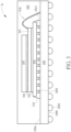
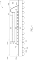
- FIG. 3 to FIG. 6 are schematic, cross-sectional diagrams showing semiconductor packages in accordance with various embodiments of the invention.
- the illustrative semiconductor packages may be a hybrid CSP having a flip-chip die and a wire-bonded die stacked on the flip-chip die.
- the semiconductor package 3a comprises a base 100 having a top surface 100a and a bottom surface 100b.
- a plurality of connecting elements 1002 such as solder balls may be disposed on the bottom surface 100b for further connection.
- a semiconductor chip 101 is mounted on the top surface 100a of the base 100.
- the semiconductor chip 101 may be a system-on-a-chip (SoC) and may generate heat during operation.
- SoC system-on-a-chip
- the semiconductor chip 101 may be mounted on the top surface 100a in a flip-chip manner by aligning and connecting the bumps (micro bumps or copper pillar bumps) 1011 on the active surface of the semiconductor chip 101 with the matching pads 1001 on the top surface 100a of the base 100.
- An optional underfill 110 may be applied to fill the gap between the semiconductor chip 101 and the top surface 100a of the base 100.
- a semiconductor chip (or package) 103 may be stacked directly on the semiconductor chip 101 and may be electrically coupled to the base 10 by using wire bonding WB.
- the semiconductor chip 103 may be a memory chip;
- the semiconductor chip 103 may be a Known Good Die (KGD) chip, but is not limited thereto.
- the semiconductor chip 103 may be adhered to the top surface of the semiconductor chip 101 by using a die attach film (DAF) 102 comprising, for example, an epoxy adhesive layer.
- DAF die attach film
- the DAF 102 has thermal conductivity of about 0.3 W/m-K.
- the semiconductor package 3a further comprises an in-package heat dissipating element 105 such as a dummy silicon die that is adhered on the top surface of the semiconductor chip 103 by using a high-thermal conductive die attach film (high-thermal conductive DAF) 104.
- the high-thermal conductive DAF 104 is an adhesive film with high thermal conductive property.
- the high-thermal conductive DAF 104 has a higher thermal conductivity than that of the DAF 102.
- the high-thermal conductive DAF 104 may have thermal conductivity of about 2-50 W/m-K.
- the semiconductor package 3a further comprises a molding compound 500 that encapsulates the semiconductor die 101, the semiconductor die 103, and the heat dissipating element 105.
- the molding compound 500 may have thermal conductivity of about 2-8 W/m-K; for another example, the molding compound 500 may have thermal conductivity of 1 W/m-K.
- the semiconductor package 3b comprises a base 100, a semiconductor chip 101 such as an SoC mounted on the base 100 in a flip-chip manner, a semiconductor chip 103 such as a DRAM chip adhered onto the semiconductor chip 101 by using a DAF 102, a heat dissipating element 104 such as a dummy silicon die adhered onto the semiconductor chip 103 by using a high-thermal conductive DAF 104.
- the difference between the semiconductor package 3a in FIG. 3 and the semiconductor package 3b in FIG. 4 is that the top surface 105a of the heat dissipating element 105 is exposed to air.
- the molding compound 500 may be subjected to a polishing or grinding process. After removing a portion of the molding compound 500, the top surface 105a of the heat dissipating element 105 may be flush with the top surface of the molding compound 500.
- the heat dissipating element 105 of the semiconductor package 5a is attached to the top surface of the semiconductor die 101 by using a high-thermal conductive DAF 104 as previously described. Therefore, the semiconductor die 103 and the heat dissipating element 105 are both attached onto the top surface of the semiconductor die 101 in a side-by-side manner.
- the semiconductor package 5b comprises a base 100, a semiconductor chip 101 such as an SoC mounted on the base 100 in a flip-chip manner, a semiconductor chip 103 such as a DRAM chip adhered onto the semiconductor chip 101 by using a DAF 102, a heat dissipating element 104 such as a dummy silicon die adhered onto the semiconductor chip 101 by using a high-thermal conductive DAF 104.
- the difference between the semiconductor package 5a in FIG. 5 and the semiconductor package 5b in FIG. 6 is that the top surface 105a of the heat dissipating element 105 is exposed to air.
- the semiconductor chip 101 is a major heat source of the semiconductor package 3a and the heat needs to be rapidly removed from the semiconductor package 3a to the ambient environment.
- the thermal performance is significant improved ( ⁇ 50% improvement).
- the measured theta JC ( ⁇ JC ) of the illustrative semiconductor package 5b in FIG. 6 may be about 2.20.
Landscapes
- Engineering & Computer Science (AREA)
- Microelectronics & Electronic Packaging (AREA)
- Cooling Or The Like Of Semiconductors Or Solid State Devices (AREA)
- Physics & Mathematics (AREA)
- Geometry (AREA)
- Control And Other Processes For Unpacking Of Materials (AREA)
- Wire Bonding (AREA)
Abstract
Description
- This application claims priority from
U.S. provisional application No. 62/798,589 filed January 30, 2019 U.S. provisional application No. 62/881,423 filed August 1, 2019 - As known in the art, a semiconductor chip package typically comprises an integrated circuit (IC) die and a molding compound that encapsulates the IC die. During operation, the IC die generates significant amount of heat, which can cause damage to the IC die or reduce the IC reliability. In a hybrid chip scale package (hybrid CSP), for example, the heat generated from one IC die such as an SoC die can be detrimental to the proximate IC die such as a DRAM die stacked on the SoC die, which leads to reduced overall chip performance.
- To dissipate heat away from the IC die, the semiconductor chip package is often connected with an external heat spreading structure such as a heat spreader or heat sink attached to the IC die. To spread heat to the ambient environment, the heat spreading structure is often mounted onto a contact surface of the semiconductor chip package by applying a thermal interface material (TIM) such as thermal greases or conductive polymers on the contact surface.
- However, the conventional thermal solution involving the use of TIM is not satisfactory. The conventional design using the TIM has problems such as thermal bottleneck and poor adhesion. It is desirable to have low contact resistance and good thermal interface between the IC die and the heat spreading structures for efficient heat conduction from the IC die through the heat spreading structures. It is also desirable to provide an improved heat transfer mechanism/medium employed between the components to effectively transfer heat away from the IC die.
- It is one object of the present disclosure to provide an improved semiconductor package with an improved thermal interface in order to solve the above-mentioned prior art shortcomings or problems.
- According to one aspect of the present disclosure, a semiconductor package including a base comprising an upper surface and a lower surface that is opposite to the upper surface; a radio-frequency (RF) structure embedded near the upper surface of the base; an integrated circuit (IC) die mounted on the lower surface of the base in a flip-chip manner so that a backside of the IC die is available for heat dissipation; a plurality of solder ball pads disposed on the lower surface of the base and arranged around the IC die; and a metal thermal interface layer comprising a backside metal layer that is in direct contact with the backside of the IC die, and a solder paste conformally printed on the backside metal layer.
- Preferably, the RF structure comprises a top antenna layer and a bottom antenna layer spaced apart from the top antenna layer, and at least one dielectric layer interposed between the top antenna layer and the bottom antenna layer.
- Preferably, the backside metal layer comprises Au.
- Preferably, the solder paste comprises lead-free solder comprising tin, copper, silver, bismuth, indium, zinc, or antimony.
- Preferably, the base comprises metal traces and vias for interconnection.
- Preferably, the solder ball pads are electrically connected to the RF structure of the base through the metal traces and vias.
- Preferably, the IC die is an RFIC die.
- Preferably, the semiconductor package further comprises an underfill disposed in the gap between the IC die and the lower surface of the base.
- Preferably, a combined thickness of the underfill, the IC die, and the metal thermal interface layer is substantially equal to a ball height of the solder balls measured from the lower surface of the base.
- Preferably, the solder paste is thicker than the backside metal layer.
- Another aspect of the invention provides a printed circuit board assembly including a printed circuit board having an upper surface directly facing the lower surface of the base, wherein the printed circuit board comprises an array of copper thermal pads on the upper surface of the printed circuit board, a plurality of thermal vias within the printed circuit board under the array of copper thermal pads, a heat spreading structure mounted onto a lower surface of the printed circuit board, wherein the heat spreading structure is in thermal contact with the plurality of thermal vias. The semiconductor package as described above is mounted on the array of copper thermal pads.
- Preferably, the plurality of thermal vias comprises plated though holes.
- Preferably, the heat spreading structure comprises a heat sink.
- Preferably, the solder paste is in direct contact with the array of copper thermal pads.
- Preferably, the array of copper thermal pads comprises slits between the thermal pads and the slits are filled with the solder paste.
- These and other objectives of the present invention will no doubt become obvious to those of ordinary skill in the art after reading the following detailed description of the preferred embodiment that is illustrated in the various figures and drawings.
- The present invention can be more fully understood by reading the subsequent detailed description and examples with references made to the accompanying drawings, wherein:
-
Fig. 1 is a cross-sectional view of a semiconductor package according to one embodiment of the disclosure; -
FIG. 2 is a schematic, cross-sectional diagram showing an exemplary PCB assembly including the semiconductor package inFIG. 1 according to one embodiment of the invention; and -
FIG. 3 to FIG. 6 are schematic, cross-sectional diagrams showing semiconductor packages in accordance with various embodiment of the invention. - The following description is of the best-contemplated mode of carrying out the invention. This description is made for the purpose of illustrating the general principles of the invention and should not be taken in a limiting sense. The scope of the invention is determined by reference to the appended claims.
- The present invention will be described with respect to particular embodiments and with reference to certain drawings, but the invention is not limited thereto and is only limited by the claims. The drawings described are only schematic and are non-limiting. In the drawings, the size of some of the elements may be exaggerated for illustrative purposes and not drawn to scale. The dimensions and the relative dimensions do not correspond to actual dimensions in the practice of the invention.
- In general, the present disclosure pertains to a semiconductor package comprising at least one integrated circuit (IC) die attached to a substrate in, for example, a "flip chip" configuration. In such a flip chip configuration, bumps are formed on signal pads or terminals of the IC die, and the IC die may be inverted ("flipped") and attached to substrate by reflowing bumps so that they attach to corresponding pads on the surface of substrate. The IC die may be one of the many types of IC dies. For example, IC die may be a radio-frequency (RF) IC die, a microprocessor die, an application-specific integrated circuit (ASIC), or a memory die according to various embodiments.
- The substrate may be one of the different types of substrates known to those skilled in the relevant arts (e.g., organic or inorganic substrates). The substrate may be made from one or more conductive layers bonded with a dielectric material. For example, the dielectric material may be made from various substances, such as bismaleimide triazine (BT). The conductive layers may be made from a metal, or combination of metals, such as copper and aluminum, that facilitate coupling between IC die and solder balls. Trace or routing patterns may be made in the conductive layer by, for example, etching the conductive layer. The substrate may be a single-layer, a two-layer, or multi-layer substrate.
- The exemplary semiconductor package may be a RFIC chip package with antenna array structure that is particularly suited for millimeter wave (mmW) applications or radar systems. However, it is to be appreciated that the principles of the present invention should not be limited to any particular package type or IC die. Rather, the principles of the invention are directed broadly to techniques for improved thermal interface material application in the fabrication process of a printed circuit board (PCB) assembly that includes an integrated circuit package and a heat transfer device.
-
FIG. 1 is a schematic, cross-sectional diagram showing an exemplary semiconductor package in accordance with one embodiment of the invention. As shown inFIG. 1 , thesemiconductor package 1 comprises abase 10 having a radio-frequency (RF)structure 11 embedded near anupper surface 10a of thebase 10. In some embodiment, thebase 10 could be a package substrate, a silicon interposer or a printed circuit board (PCB). In other embodiments, the radio-frequency (RF)structure 11 may comprise an antenna array, for example, the radio-frequency (RF)structure 11 may comprise atop antenna layer 111 and abottom antenna layer 112 spaced apart from thetop antenna layer 111. For example, at least onedielectric layer 113 may be interposed between thetop antenna layer 111 and thebottom antenna layer 112. Preferably, thetop antenna layer 111 and thebottom antenna layer 112 may be formed in the upper metal layers of thebase 10, but not limited thereto. Thebase 10 may comprisemetal traces 114 andvias 115 for interconnection. - Preferably, for example, the
semiconductor package 1 may further comprise an IC die 20 such as an RFIC die mounted on thelower surface 10b of thebase 10. The IC die 20 may be mounted on thelower surface 10b in a flip-chip manner so that the backside 20b of the IC die 20 is exposed and available for heat dissipation. The flip-chip type connection is a method for interconnecting a flipped IC die 20 to external circuitry withbumps 202 such as micro bumps or copper pillar bumps disposed on the chip pads of the IC die 20. Thebumps 202 are aligned with and electrically connected to thecopper pads 116 disposed at thelower surface 10b of thebase 10. Optionally, anunderfill 210 may be applied to the gap between the IC die 20 and thelower surface 10b of thebase 10. - Preferably, for example, the
semiconductor package 1 may further comprise a plurality ofconductive pads 118 disposed on thelower surface 10b of thebase 10 and arranged around the IC die 20. Theconductive pads 118 may be electrically connected to the circuit including theRF structure 11 of the base 10 through the metal traces 114 andvias 115. A plurality ofconductive structures 120 such as ball grid array (BGA) balls may be disposed on theconductive pads 118, respectively, for electrically connecting the circuit including theRF structure 11 of the base 10 with the external circuit device such as a printed circuit board (PCB). - Preferably, for example, the
semiconductor package 1 may further comprise a metalthermal interface layer 30. The metalthermal interface layer 30 may be a metal bi-layer structure comprising abackside metal layer 310 that is in direct contact with the backside 20b of the IC die 20, and asolder paste 320 conformally printed on thebackside metal layer 310. Preferably, thebackside metal layer 310 may comprise Au, but not limited thereto. For example, thebackside metal layer 310 may be Au layer that is sputtered onto the backside 20b of the IC die 20. - For example, the solder paste (or pre-solder) 320 may be formed by stencil printing methods, but not limited thereto. For example, the
solder paste 320 may comprise any lead-free solders in commercial use, which may contain tin, copper, silver, bismuth, indium, zinc, antimony, and traces of other metals. Preferably, for example, thesolder paste 320 may be thicker than thebackside metal layer 310. It is noteworthy that the metalthermal interface layer 30 does not comprise a conventional thermal interface material (TIM) such as thermal grease or conductive polymer. - Preferably, the combined thickness of the
underfill 210, the IC die 20, and the metalthermal interface layer 30 is substantially equal to the ball height h of theconductive structures 120 measured from thelower surface 10b of thebase 10. - Please refer to
FIG. 2. FIG. 2 is a schematic, cross-sectional diagram showing an exemplary PCB assembly including the semiconductor package inFIG. 1 according to one embodiment of the invention. As shown inFIG. 2 , the exemplary PCB assembly 2 comprises a PCB 4 having anupper surface 4a directly facing thelower surface 10b of thebase 10. Preferably, an array of copperthermal pads 410 may be disposed within a solder resistopening 402a in the solder resistlayer 402 on theupper surface 4a of the PCB 4. - Preferably, the span of the array of conductive
thermal pads 410 may be in commensurate with the area of the backside 20b of the IC die 20. Preferably, the span of the array of conductivethermal pads 410 may be slightly greater than the area of the backside 20b of the IC die 20. For example, the distance from the edge of the IC die 20 to the perimeter of the array of conductivethermal pads 410 may be about 150 micrometers, but not limited thereto. - Preferably, slits or
gaps 411 may be formed between the adjacent conductivethermal pads 410. Preferably, a plurality ofthermal vias 420 is formed within the PCB 4 under the array of the conductivethermal pads 410. Preferably, thethermal vias 420 are in thermal contact with the conductivethermal pads 410, respectively. Preferably, thethermal vias 420 are plated though holes. Preferably, a heat spreading structure 5 such as a heat sink may be mounted onto thelower surface 4b of the PCB 4. The heat spreading structure 5 is in thermal contact with thethermal vias 420. - Preferably, the
semiconductor package 1 as depicted inFIG. 1 is mounted onto theupper surface 4a of the PCB 4 such that thesolder paste 320 is laminated onto the array of conductivethermal pads 410. With suitable pressing force, thesolder paste 320 may be forced (or squeezed) into theslits 411. By providing such configuration, more heat dissipating surface area may be produced. Theconductive structures 120 are aligned with matchingpads 412 on theupper surface 4a of the PCB 4. Thesolder paste 320 and theconductive structures 120 may be subjected to a reflow process so as to form permanent bond. The metalthermal interface layer 30 is used as a high-efficiency heat transfer medium that allows heat energy to rapidly move from the IC die 20 to the conductivethermal pads 410 and platedthermal vias 420 of the PCB 40 to the heat spreading structure 5. Further, it is advantageous to use the present invention because the adhesion between thesemiconductor package 1 and the PCB 4 can be significantly improved. - Please refer to
FIG. 3 to FIG. 6. FIG. 3 to FIG. 6 are schematic, cross-sectional diagrams showing semiconductor packages in accordance with various embodiments of the invention. For example, the illustrative semiconductor packages may be a hybrid CSP having a flip-chip die and a wire-bonded die stacked on the flip-chip die. - As shown in
FIG. 3 , the semiconductor package 3a comprises a base 100 having atop surface 100a and abottom surface 100b. A plurality of connectingelements 1002 such as solder balls may be disposed on thebottom surface 100b for further connection. Asemiconductor chip 101 is mounted on thetop surface 100a of thebase 100. In a non-limiting example, thesemiconductor chip 101 may be a system-on-a-chip (SoC) and may generate heat during operation. - Preferably, the
semiconductor chip 101 may be mounted on thetop surface 100a in a flip-chip manner by aligning and connecting the bumps (micro bumps or copper pillar bumps) 1011 on the active surface of thesemiconductor chip 101 with thematching pads 1001 on thetop surface 100a of thebase 100. Anoptional underfill 110 may be applied to fill the gap between thesemiconductor chip 101 and thetop surface 100a of thebase 100. - Preferably, a semiconductor chip (or package) 103 may be stacked directly on the
semiconductor chip 101 and may be electrically coupled to thebase 10 by using wire bonding WB. In a non-limiting example, thesemiconductor chip 103 may be a memory chip; In another example, thesemiconductor chip 103 may be a Known Good Die (KGD) chip, but is not limited thereto. Preferably, thesemiconductor chip 103 may be adhered to the top surface of thesemiconductor chip 101 by using a die attach film (DAF) 102 comprising, for example, an epoxy adhesive layer. Preferably, for example, theDAF 102 has thermal conductivity of about 0.3 W/m-K. - Preferably, the semiconductor package 3a further comprises an in-package
heat dissipating element 105 such as a dummy silicon die that is adhered on the top surface of thesemiconductor chip 103 by using a high-thermal conductive die attach film (high-thermal conductive DAF) 104. Preferably, the high-thermalconductive DAF 104 is an adhesive film with high thermal conductive property. Preferably, the high-thermalconductive DAF 104 has a higher thermal conductivity than that of theDAF 102. Preferably, for example, the high-thermalconductive DAF 104 may have thermal conductivity of about 2-50 W/m-K. - Preferably, the semiconductor package 3a further comprises a
molding compound 500 that encapsulates the semiconductor die 101, the semiconductor die 103, and theheat dissipating element 105. Preferably, for example, themolding compound 500 may have thermal conductivity of about 2-8 W/m-K; for another example, themolding compound 500 may have thermal conductivity of 1 W/m-K. - In
FIG. 4 , likewise, thesemiconductor package 3b comprises abase 100, asemiconductor chip 101 such as an SoC mounted on the base 100 in a flip-chip manner, asemiconductor chip 103 such as a DRAM chip adhered onto thesemiconductor chip 101 by using aDAF 102, aheat dissipating element 104 such as a dummy silicon die adhered onto thesemiconductor chip 103 by using a high-thermalconductive DAF 104. The difference between the semiconductor package 3a inFIG. 3 and thesemiconductor package 3b inFIG. 4 is that thetop surface 105a of theheat dissipating element 105 is exposed to air. To form such configuration, themolding compound 500 may be subjected to a polishing or grinding process. After removing a portion of themolding compound 500, thetop surface 105a of theheat dissipating element 105 may be flush with the top surface of themolding compound 500. - In
FIG. 5 , instead of attaching theheat dissipating element 105 onto the semiconductor die 103, theheat dissipating element 105 of thesemiconductor package 5a is attached to the top surface of the semiconductor die 101 by using a high-thermalconductive DAF 104 as previously described. Therefore, the semiconductor die 103 and theheat dissipating element 105 are both attached onto the top surface of the semiconductor die 101 in a side-by-side manner. - In
FIG. 6 , likewise, thesemiconductor package 5b comprises abase 100, asemiconductor chip 101 such as an SoC mounted on the base 100 in a flip-chip manner, asemiconductor chip 103 such as a DRAM chip adhered onto thesemiconductor chip 101 by using aDAF 102, aheat dissipating element 104 such as a dummy silicon die adhered onto thesemiconductor chip 101 by using a high-thermalconductive DAF 104. The difference between thesemiconductor package 5a inFIG. 5 and thesemiconductor package 5b inFIG. 6 is that thetop surface 105a of theheat dissipating element 105 is exposed to air. - Preferably, the
semiconductor chip 101 is a major heat source of the semiconductor package 3a and the heat needs to be rapidly removed from the semiconductor package 3a to the ambient environment. By providing the configuration throughFIG. 3 to FIG. 6 , the thermal performance is significant improved (~50% improvement). For example, the measured theta JC (θJC) of theillustrative semiconductor package 5b inFIG. 6 may be about 2.20. - Those skilled in the art will readily observe that numerous modifications and alterations of the device and method may be made while retaining the teachings of the invention. Accordingly, the above disclosure should be construed as limited only by the metes and bounds of the appended claims.
The present invention can also be described by means of the following clauses: - 1. A semiconductor package (1), comprising:
- a base (10) comprising an upper surface (10a) and a lower surface (10b) that is opposite to the upper surface (10a);
- a radio-frequency, in the following also referred to as RF, structure (11) embedded near the upper surface (10a) of the base (10);
- an integrated circuit, in the following also referred to as IC, die (20) mounted on the lower surface (10b) of the base (10) in a flip-chip manner so that a backside (20b) of the IC die (20) is available for heat dissipation;
- a plurality of conductive structures (118, 120) disposed on the lower surface (10b) of the base (10) and arranged around the IC die (20); and
- a metal thermal interface layer (30) comprising a backside metal layer (310) that is in direct contact with the backside (20b) of the IC die (20), and a solder paste (320) conformally printed on the backside metal layer (310).
- 2. The semiconductor package (1) according to
clause 1, wherein the RF structure (11) comprises a top antenna layer (111) and a bottom antenna layer (112) spaced apart from the top antenna layer (111), and at least one dielectric layer (113) interposed between the top antenna layer (111) and the bottom antenna layer (112). - 3. The semiconductor package according to
clause 1 or 2, wherein the backside metal layer (310) comprises Au. - 4. The semiconductor package according to any one of
clause 1 to 3, wherein the solder paste (320) comprises lead-free solder comprising tin, copper, silver, bismuth, indium, zinc, or antimony. - 5. The semiconductor package according to any one of
clause 1 to 4, wherein the base (10) comprises metal traces (114) and vias (115) for interconnection. - 6. The semiconductor package according to clause 5, wherein the conductive structures (118, 120) are electrically connected to the RF structure (11) of the base (10) through the metal traces (114) and vias (115).
- 7. The semiconductor package according to any one of
clauses 1 to 6, wherein the IC die (20) is an RFIC die. - 8. The semiconductor package according to any one of
clauses 1 to 7 further comprising:
an underfill (210) disposed in the gap between the IC die (20) and the lower surface (10b) of the base (10). - 9. The semiconductor package according to any one of
clauses 1 to 8, wherein a combined thickness of the underfill (210), the IC die (20), and the metal thermal interface layer (30) is substantially equal to a ball height of the conductive structures (118, 120) measured from the lower surface (10b) of the base (10). - 10. The semiconductor package according to any one of
clauses 1 to 9, wherein the solder paste (320) is thicker than the backside metal layer (310). - 11. A printed circuit board assembly (2), comprising:
- a semiconductor package (1) according to
claim 1; and - a print circuit board, in the following also referred to as PCB (4), having an upper surface (4a) directly facing the lower surface (10b) of the base (10), wherein the PCB (4) comprises an array of conductive thermal pads (410) on the upper surface (4a) of the PCB (4), a plurality of thermal vias (420) within the PCB (4) under the array of copper thermal pads (410), a heat spreading structure (5) mounted onto a lower surface (4b) of the PCB (4), wherein the heat spreading structure (5) is in thermal contact with the plurality of thermal vias (420);
- wherein the semiconductor package (1) is mounted on the array of conductive thermal pads (410).
- a semiconductor package (1) according to
- 12. The printed circuit board assembly according to
clause 11, wherein the plurality of thermal vias (420) comprises plated though holes. - 13. The printed circuit board assembly according to
clause 11 or 12, wherein the heat spreading structure (5) comprises a heat sink. - 14. The printed circuit board assembly according to any one of
clauses 11 to 13, wherein the solder paste (320) is in direct contact with the array of conductive thermal pads (410). - 15. The printed circuit board assembly according to clause 14, wherein the array of conductive thermal pads (410) comprises slits (411) between the thermal pads (410) and the slits (411) are filled with the solder paste (320).
Claims (14)
- A semiconductor package (3a; 3b), comprising:a base (100) comprising a top surface (100a) and a bottom surface (100b) that is opposite to the top surface;a first semiconductor chip (101) mounted on the top surface (100a) of the base (100) in a flip-chip manner;a second semiconductor chip (103) stacked on the first semiconductor chip (101) and electrically coupled to the base (100) by at least one connecting element;an in-package heat dissipating element (105) comprising a dummy silicon die adhered onto the second semiconductor chip (103) by using a high-thermal conductive die attach film (104); anda molding compound (500) encapsulating the first semiconductor die (101), the second semiconductor die (103), and the in-package heat dissipating element (105).
- A semiconductor package (5a; 5b), comprising:a base (100) comprising a top surface (100a) and a bottom surface (100b) that is opposite to the top surface (100a);a first semiconductor chip (101) mounted on the top surface (100a) of the base (100) in a flip-chip manner;a second semiconductor chip (103) stacked on the first semiconductor chip (101) and electrically coupled to the base (100) by at least one connecting element;an in-package heat dissipating element (105) comprising a dummy silicon die attached to a top surface of the first semiconductor chip (101) by using a high-thermal conductive die attach film (104); anda molding compound (500) encapsulating the first semiconductor die (101), the second semiconductor die (103), and the in-package heat dissipating element (105).
- The semiconductor package (5a; 5b) according to claim 2, wherein the second semiconductor die (103) and the in-package heat dissipating element (105) are attached onto the top surface of the first semiconductor chip (101) in a side-by-side manner.
- The semiconductor package (3b; 5b) according to any one of claims 1 to 3, wherein a top surface of the in-package heat dissipating element (105) is not covered by the molding compound (500) and is exposed.
- The semiconductor package (3a; 3b; 5a; 5b) according to any one of claims 1 to 4, wherein the at least one connecting element is wire bonding (WB).
- The semiconductor package (3a; 3b; 5a; 5b) according to any one of claims 1 to 5, wherein the first semiconductor chip (101) is a system-on-a-chip, in the following also referred to as SoC, and the second semiconductor chip (103) is a memory chip.
- The semiconductor package (3a; 3b; 5a; 5b) according to claim 6, wherein the memory chip (103) comprises a DRAM chip.
- The semiconductor package (3a; 3b; 5a; 5b) according to any one of claims 1 to 7, wherein the second semiconductor chip (103) is adhered to the first semiconductor chip (101) by using a die attach film (102).
- The semiconductor package (3a; 3b; 5a; 5b) according to claim 8, wherein the die attach film (102) comprises an epoxy adhesive layer.
- The semiconductor package (3a; 3b; 5a; 5b) according to claim 8 or 9, wherein the die attach film (102) has thermal conductivity of about 0.3 W/m-K.
- The semiconductor package (3a; 3b; 5a; 5b) according to any one of claims 8 to 10, wherein the high-thermal conductive die attach film (104) comprises an adhesive film with a higher thermal conductivity than that of the die attach film (102).
- The semiconductor package (3a; 3b; 5a; 5b) according to any one of claims 1 to 11, wherein the high-thermal conductive die attach film (104) has a thermal conductivity of about 2-50 W/m-K.
- The semiconductor package (3a; 3b; 5a; 5b) according to any one of claims 1 to 12, wherein the molding compound (500) has a thermal conductivity of about 2-8 W/m-K.
- The semiconductor package (3a; 3b; 5a; 5b) according to any one of claims 1 to 13, wherein the molding compound (500) has a thermal conductivity of 1W/m-K.
Applications Claiming Priority (4)
| Application Number | Priority Date | Filing Date | Title |
|---|---|---|---|
| US201962798589P | 2019-01-30 | 2019-01-30 | |
| US201962881423P | 2019-08-01 | 2019-08-01 | |
| US16/742,850 US11227846B2 (en) | 2019-01-30 | 2020-01-14 | Semiconductor package having improved thermal interface between semiconductor die and heat spreading structure |
| EP20152026.9A EP3690935B1 (en) | 2019-01-30 | 2020-01-15 | Semiconductor package having improved thermal interface between semiconductor die and heat spreading structure |
Related Parent Applications (2)
| Application Number | Title | Priority Date | Filing Date |
|---|---|---|---|
| EP20152026.9A Division-Into EP3690935B1 (en) | 2019-01-30 | 2020-01-15 | Semiconductor package having improved thermal interface between semiconductor die and heat spreading structure |
| EP20152026.9A Division EP3690935B1 (en) | 2019-01-30 | 2020-01-15 | Semiconductor package having improved thermal interface between semiconductor die and heat spreading structure |
Publications (2)
| Publication Number | Publication Date |
|---|---|
| EP4428913A2 true EP4428913A2 (en) | 2024-09-11 |
| EP4428913A3 EP4428913A3 (en) | 2025-03-12 |
Family
ID=69172727
Family Applications (2)
| Application Number | Title | Priority Date | Filing Date |
|---|---|---|---|
| EP24191249.2A Pending EP4428913A3 (en) | 2019-01-30 | 2020-01-15 | Semiconductor package having improved thermal interface between semiconductor die and heat spreading structure |
| EP20152026.9A Active EP3690935B1 (en) | 2019-01-30 | 2020-01-15 | Semiconductor package having improved thermal interface between semiconductor die and heat spreading structure |
Family Applications After (1)
| Application Number | Title | Priority Date | Filing Date |
|---|---|---|---|
| EP20152026.9A Active EP3690935B1 (en) | 2019-01-30 | 2020-01-15 | Semiconductor package having improved thermal interface between semiconductor die and heat spreading structure |
Country Status (4)
| Country | Link |
|---|---|
| US (4) | US11227846B2 (en) |
| EP (2) | EP4428913A3 (en) |
| CN (2) | CN111508947A (en) |
| TW (2) | TWI742517B (en) |
Families Citing this family (30)
| Publication number | Priority date | Publication date | Assignee | Title |
|---|---|---|---|---|
| US9515017B2 (en) * | 2014-12-18 | 2016-12-06 | Intel Corporation | Ground via clustering for crosstalk mitigation |
| US11227846B2 (en) | 2019-01-30 | 2022-01-18 | Mediatek Inc. | Semiconductor package having improved thermal interface between semiconductor die and heat spreading structure |
| US11456227B2 (en) * | 2019-12-17 | 2022-09-27 | Nxp Usa, Inc. | Topside heatsinking antenna launcher for an integrated circuit package |
| WO2022004178A1 (en) * | 2020-07-02 | 2022-01-06 | ソニーセミコンダクタソリューションズ株式会社 | Interposer, circuit device, interposer manufacturing method, and circuit device manufacturing method |
| KR102854683B1 (en) * | 2020-12-02 | 2025-09-03 | 에스케이하이닉스 주식회사 | Semiconductor packages including heat dissipation layer |
| WO2022118645A1 (en) * | 2020-12-02 | 2022-06-09 | 株式会社村田製作所 | Integrated circuit and high-frequency module |
| US11817366B2 (en) | 2020-12-07 | 2023-11-14 | Nxp Usa, Inc. | Semiconductor device package having thermal dissipation feature and method therefor |
| US12322856B2 (en) * | 2020-12-30 | 2025-06-03 | Texas Instruments Incorporated | Antenna in package having antenna on package substrate |
| US11538790B2 (en) * | 2021-03-22 | 2022-12-27 | Broadcom International Pte. Ltd. | Extended HBM offsets in 2.5D interposers |
| US11967538B2 (en) | 2021-04-09 | 2024-04-23 | Google Llc | Three dimensional IC package with thermal enhancement |
| CN115241636A (en) * | 2021-04-23 | 2022-10-25 | 鹏鼎控股(深圳)股份有限公司 | Antenna module and its manufacturing method and terminal |
| US12406896B2 (en) * | 2021-04-27 | 2025-09-02 | Nxp Usa, Inc. | Semiconductor device package having thermal dissipation feature and method therefor |
| KR102935371B1 (en) * | 2021-05-03 | 2026-03-06 | 삼성전자주식회사 | Semiconductor package and method of fabricating the same |
| JP7623588B2 (en) * | 2021-08-06 | 2025-01-29 | 富士通株式会社 | Electronic component embedded package and electronic device |
| US20230116326A1 (en) * | 2021-10-13 | 2023-04-13 | Mediatek Inc. | Semiconductor package with tsv die |
| FR3129809B1 (en) * | 2021-11-30 | 2024-05-10 | St Microelectronics Grenoble 2 | Heat dissipation |
| TWI790054B (en) | 2021-12-17 | 2023-01-11 | 財團法人工業技術研究院 | Integrated antenna package structure |
| US12315853B2 (en) * | 2022-01-24 | 2025-05-27 | Apple Inc. | System packaging for cellular modem and transceiver system of heterogeneous stacking |
| TWI793024B (en) * | 2022-05-26 | 2023-02-11 | 矽品精密工業股份有限公司 | Electronic package and manufacturing method thereof |
| US20230395461A1 (en) * | 2022-06-06 | 2023-12-07 | Taiwan Semiconductor Manufacturing Co., Ltd. | Semiconductor Device and Method Forming Same |
| US12412879B2 (en) * | 2022-06-09 | 2025-09-09 | Unimicron Technology Corp. | Package structure and manufacturing method thereof |
| CN115360499B (en) * | 2022-07-21 | 2025-08-26 | 北京遥测技术研究所 | A W-band two-dimensional AIP microsystem architecture |
| CN115802588B (en) * | 2022-11-21 | 2025-04-11 | 四川九洲电器集团有限责任公司 | A ball grid array device heat dissipation printed circuit board |
| US20250174517A1 (en) * | 2023-11-29 | 2025-05-29 | Taiwan Semiconductor Manufacturing Co., Ltd. | Integrated circuit packages and methods of forming the same |
| US20250183237A1 (en) * | 2023-12-01 | 2025-06-05 | Taiwan Semiconductor Manufacturing Company Limited | Package structure including a backside metal film on a semiconductor die and a thermally conductive underfill layer on the backside metal film and methods of forming the same |
| US20250192100A1 (en) * | 2023-12-07 | 2025-06-12 | Taiwan Semiconductor Manufacturing Company, Ltd. | System on integrated circuit structure |
| US20250201650A1 (en) * | 2023-12-14 | 2025-06-19 | Taiwan Semiconductor Manufacturing Company, Ltd. | Chip package structure and method for forming the same |
| US20250279358A1 (en) * | 2024-02-29 | 2025-09-04 | Taiwan Semiconductor Manufacturing Company, Ltd. | Integrated circuit structures and methods of forming the same |
| US20250364351A1 (en) | 2024-05-22 | 2025-11-27 | Nanya Technology Corporation | Package structure including heat sink structure and method for manufacturing the same |
| WO2026080361A1 (en) * | 2024-10-13 | 2026-04-16 | Applied Materials, Inc. | Chip-on-glass architecture for thermal dissipation |
Family Cites Families (27)
| Publication number | Priority date | Publication date | Assignee | Title |
|---|---|---|---|---|
| JP2914342B2 (en) * | 1997-03-28 | 1999-06-28 | 日本電気株式会社 | Cooling structure of integrated circuit device |
| JP2000236051A (en) * | 1999-02-16 | 2000-08-29 | Internatl Business Mach Corp <Ibm> | Radiator for cooling electronic circuit chips |
| TW445610B (en) * | 2000-06-16 | 2001-07-11 | Siliconware Precision Industries Co Ltd | Stacked-die packaging structure |
| US6734552B2 (en) | 2001-07-11 | 2004-05-11 | Asat Limited | Enhanced thermal dissipation integrated circuit package |
| US6818980B1 (en) | 2003-05-07 | 2004-11-16 | Asat Ltd. | Stacked semiconductor package and method of manufacturing the same |
| US7269017B2 (en) * | 2004-11-19 | 2007-09-11 | Delphi Technologies, Inc. | Thermal management of surface-mount circuit devices on laminate ceramic substrate |
| US20070164446A1 (en) * | 2006-01-13 | 2007-07-19 | Hawk Donald E Jr | Integrated circuit having second substrate to facilitate core power and ground distribution |
| US7683467B2 (en) * | 2006-12-07 | 2010-03-23 | Stats Chippac Ltd. | Integrated circuit package system employing structural support |
| US7675465B2 (en) * | 2007-05-22 | 2010-03-09 | Sibeam, Inc. | Surface mountable integrated circuit packaging scheme |
| US8013440B2 (en) * | 2008-03-28 | 2011-09-06 | Conexant Systems, Inc. | Enhanced thermal dissipation ball grid array package |
| TWI388041B (en) * | 2008-11-11 | 2013-03-01 | 矽品精密工業股份有限公司 | Semiconductor package with heat dissipation structure |
| US20120126396A1 (en) | 2010-11-19 | 2012-05-24 | Broadcom Corporation | Die down device with thermal connector |
| EP2766931B1 (en) * | 2011-10-03 | 2021-12-01 | Invensas Corporation | Stub minimization for wirebond assemblies without windows |
| US8779599B2 (en) * | 2011-11-16 | 2014-07-15 | Taiwan Semiconductor Manufacturing Company, Ltd. | Packages including active dies and dummy dies and methods for forming the same |
| WO2014129351A1 (en) * | 2013-02-21 | 2014-08-28 | ピーエスフォー ルクスコ エスエイアールエル | Semiconductor device and method for manufacturing same |
| US9620464B2 (en) * | 2014-08-13 | 2017-04-11 | International Business Machines Corporation | Wireless communications package with integrated antennas and air cavity |
| US10446541B2 (en) * | 2015-09-14 | 2019-10-15 | Intel IP Corporation | Advanced node cost reduction by ESD interposer |
| WO2017171889A1 (en) * | 2016-04-02 | 2017-10-05 | Intel Corporation | Systems, methods, and apparatuses for implementing a thermal solution for 3d packaging |
| KR102534732B1 (en) * | 2016-06-14 | 2023-05-19 | 삼성전자 주식회사 | semiconductor package |
| US10687447B2 (en) | 2016-10-14 | 2020-06-16 | Laird Technologies, Inc. | Methods of applying thermal interface materials to board level shields |
| US10424559B2 (en) | 2016-12-22 | 2019-09-24 | Intel Corporation | Thermal management of molded packages |
| WO2018207600A1 (en) * | 2017-05-11 | 2018-11-15 | 株式会社村田製作所 | Circuit module |
| KR102179166B1 (en) | 2017-05-19 | 2020-11-16 | 삼성전자주식회사 | Antenna substrate and semiconductor combined module |
| CN209029363U (en) | 2018-11-23 | 2019-06-25 | 北京比特大陆科技有限公司 | Chip cooling structure, chip structure, circuit board and supercomputer equipment |
| DE102018115509A1 (en) * | 2018-06-27 | 2020-01-02 | Infineon Technologies Ag | Heat dissipation device, semiconductor packaging system and method of manufacturing the same |
| CN209029362U (en) | 2018-11-23 | 2019-06-25 | 北京比特大陆科技有限公司 | Chip cooling structure, chip structure, circuit board and supercomputer equipment |
| US11227846B2 (en) | 2019-01-30 | 2022-01-18 | Mediatek Inc. | Semiconductor package having improved thermal interface between semiconductor die and heat spreading structure |
-
2020
- 2020-01-14 US US16/742,850 patent/US11227846B2/en active Active
- 2020-01-15 EP EP24191249.2A patent/EP4428913A3/en active Pending
- 2020-01-15 EP EP20152026.9A patent/EP3690935B1/en active Active
- 2020-01-17 CN CN202010052472.7A patent/CN111508947A/en active Pending
- 2020-01-17 CN CN202211415765.2A patent/CN115884499A/en active Pending
- 2020-01-20 TW TW109101878A patent/TWI742517B/en active
- 2020-01-20 TW TW110123250A patent/TWI773404B/en active
- 2020-02-27 US US16/802,576 patent/US11302657B2/en active Active
-
2021
- 2021-12-14 US US17/549,901 patent/US11705413B2/en active Active
-
2022
- 2022-03-04 US US17/687,350 patent/US11967570B2/en active Active
Also Published As
| Publication number | Publication date |
|---|---|
| EP3690935A1 (en) | 2020-08-05 |
| US11967570B2 (en) | 2024-04-23 |
| TWI773404B (en) | 2022-08-01 |
| EP3690935B1 (en) | 2025-01-08 |
| TW202137433A (en) | 2021-10-01 |
| US20200243464A1 (en) | 2020-07-30 |
| US20220285297A1 (en) | 2022-09-08 |
| US11705413B2 (en) | 2023-07-18 |
| US11302657B2 (en) | 2022-04-12 |
| US20200243462A1 (en) | 2020-07-30 |
| EP4428913A3 (en) | 2025-03-12 |
| CN111508947A (en) | 2020-08-07 |
| US20220102297A1 (en) | 2022-03-31 |
| TWI742517B (en) | 2021-10-11 |
| TW202029426A (en) | 2020-08-01 |
| CN115884499A (en) | 2023-03-31 |
| US11227846B2 (en) | 2022-01-18 |
Similar Documents
| Publication | Publication Date | Title |
|---|---|---|
| US11705413B2 (en) | Semiconductor package having improved thermal interface between semiconductor die and heat spreading structure | |
| US12002721B2 (en) | Method of fabricating semiconductor structure | |
| US6555906B2 (en) | Microelectronic package having a bumpless laminated interconnection layer | |
| US20240312864A1 (en) | Package structure and manufacturing method thereof | |
| TWI529878B (en) | Integrated circuit package and assembly method thereof | |
| KR100533673B1 (en) | Semiconductor device, method of manufacture thereof, circuit board, and electronic device | |
| KR100856609B1 (en) | A semiconductor device and a method of manufacturing the same | |
| US9953907B2 (en) | PoP device | |
| US7554185B2 (en) | Flip chip and wire bond semiconductor package | |
| KR100698526B1 (en) | A wiring board having a heat dissipation layer and a semiconductor package using the same | |
| US20030214049A1 (en) | Heat dissipating flip-chip ball grid array | |
| KR20150094135A (en) | Semiconductor package and manufacturing the same | |
| US20230326881A1 (en) | Semiconductor package with riveting structure between two rings and method for forming the same | |
| US20210090970A1 (en) | Integrated device package | |
| TW200408088A (en) | Process for fabricating semiconductor package having heat spreader and the same thereof | |
| JPWO2001018864A1 (en) | Semiconductor device and manufacturing method thereof, circuit board and electronic device |
Legal Events
| Date | Code | Title | Description |
|---|---|---|---|
| PUAI | Public reference made under article 153(3) epc to a published international application that has entered the european phase |
Free format text: ORIGINAL CODE: 0009012 |
|
| STAA | Information on the status of an ep patent application or granted ep patent |
Free format text: STATUS: THE APPLICATION HAS BEEN PUBLISHED |
|
| AC | Divisional application: reference to earlier application |
Ref document number: 3690935 Country of ref document: EP Kind code of ref document: P |
|
| AK | Designated contracting states |
Kind code of ref document: A2 Designated state(s): AL AT BE BG CH CY CZ DE DK EE ES FI FR GB GR HR HU IE IS IT LI LT LU LV MC MK MT NL NO PL PT RO RS SE SI SK SM TR |
|
| REG | Reference to a national code |
Ref country code: DE Ref legal event code: R079 Free format text: PREVIOUS MAIN CLASS: H01L0023000000 Ipc: H01L0023367000 |
|
| RIC1 | Information provided on ipc code assigned before grant |
Ipc: H01L 23/31 20060101ALN20241112BHEP Ipc: H01L 25/18 20230101ALN20241112BHEP Ipc: H01L 25/065 20230101ALI20241112BHEP Ipc: H01L 23/367 20060101AFI20241112BHEP |
|
| PUAL | Search report despatched |
Free format text: ORIGINAL CODE: 0009013 |
|
| AK | Designated contracting states |
Kind code of ref document: A3 Designated state(s): AL AT BE BG CH CY CZ DE DK EE ES FI FR GB GR HR HU IE IS IT LI LT LU LV MC MK MT NL NO PL PT RO RS SE SI SK SM TR |
|
| RIC1 | Information provided on ipc code assigned before grant |
Ipc: H01L 23/31 20060101ALN20250205BHEP Ipc: H01L 25/18 20230101ALN20250205BHEP Ipc: H01L 25/065 20230101ALI20250205BHEP Ipc: H01L 23/367 20060101AFI20250205BHEP |
|
| STAA | Information on the status of an ep patent application or granted ep patent |
Free format text: STATUS: REQUEST FOR EXAMINATION WAS MADE |
|
| 17P | Request for examination filed |
Effective date: 20250901 |