EP4428845A1 - Ansteuerungsvorrichtung und ansteuerungsverfahren für led-anzeigebildschirm und led-anzeigebildschirm - Google Patents
Ansteuerungsvorrichtung und ansteuerungsverfahren für led-anzeigebildschirm und led-anzeigebildschirm Download PDFInfo
- Publication number
- EP4428845A1 EP4428845A1 EP21965250.0A EP21965250A EP4428845A1 EP 4428845 A1 EP4428845 A1 EP 4428845A1 EP 21965250 A EP21965250 A EP 21965250A EP 4428845 A1 EP4428845 A1 EP 4428845A1
- Authority
- EP
- European Patent Office
- Prior art keywords
- led display
- light
- pixel circuit
- emitting diode
- temperature value
- Prior art date
- Legal status (The legal status is an assumption and is not a legal conclusion. Google has not performed a legal analysis and makes no representation as to the accuracy of the status listed.)
- Pending
Links
Images



Classifications
-
- G—PHYSICS
- G09—EDUCATION; CRYPTOGRAPHY; DISPLAY; ADVERTISING; SEALS
- G09G—ARRANGEMENTS OR CIRCUITS FOR CONTROL OF INDICATING DEVICES USING STATIC MEANS TO PRESENT VARIABLE INFORMATION
- G09G3/00—Control arrangements or circuits, of interest only in connection with visual indicators other than cathode-ray tubes
- G09G3/20—Control arrangements or circuits, of interest only in connection with visual indicators other than cathode-ray tubes for presentation of an assembly of a number of characters, e.g. a page, by composing the assembly by combination of individual elements arranged in a matrix no fixed position being assigned to or needed to be assigned to the individual characters or partial characters
- G09G3/22—Control arrangements or circuits, of interest only in connection with visual indicators other than cathode-ray tubes for presentation of an assembly of a number of characters, e.g. a page, by composing the assembly by combination of individual elements arranged in a matrix no fixed position being assigned to or needed to be assigned to the individual characters or partial characters using controlled light sources
- G09G3/30—Control arrangements or circuits, of interest only in connection with visual indicators other than cathode-ray tubes for presentation of an assembly of a number of characters, e.g. a page, by composing the assembly by combination of individual elements arranged in a matrix no fixed position being assigned to or needed to be assigned to the individual characters or partial characters using controlled light sources using electroluminescent panels
- G09G3/32—Control arrangements or circuits, of interest only in connection with visual indicators other than cathode-ray tubes for presentation of an assembly of a number of characters, e.g. a page, by composing the assembly by combination of individual elements arranged in a matrix no fixed position being assigned to or needed to be assigned to the individual characters or partial characters using controlled light sources using electroluminescent panels semiconductive, e.g. using light-emitting diodes [LED]
-
- G—PHYSICS
- G09—EDUCATION; CRYPTOGRAPHY; DISPLAY; ADVERTISING; SEALS
- G09G—ARRANGEMENTS OR CIRCUITS FOR CONTROL OF INDICATING DEVICES USING STATIC MEANS TO PRESENT VARIABLE INFORMATION
- G09G3/00—Control arrangements or circuits, of interest only in connection with visual indicators other than cathode-ray tubes
- G09G3/20—Control arrangements or circuits, of interest only in connection with visual indicators other than cathode-ray tubes for presentation of an assembly of a number of characters, e.g. a page, by composing the assembly by combination of individual elements arranged in a matrix no fixed position being assigned to or needed to be assigned to the individual characters or partial characters
- G09G3/2007—Display of intermediate tones
- G09G3/2077—Display of intermediate tones by a combination of two or more gradation control methods
- G09G3/2081—Display of intermediate tones by a combination of two or more gradation control methods with combination of amplitude modulation and time modulation
-
- G—PHYSICS
- G09—EDUCATION; CRYPTOGRAPHY; DISPLAY; ADVERTISING; SEALS
- G09G—ARRANGEMENTS OR CIRCUITS FOR CONTROL OF INDICATING DEVICES USING STATIC MEANS TO PRESENT VARIABLE INFORMATION
- G09G2300/00—Aspects of the constitution of display devices
- G09G2300/08—Active matrix structure, i.e. with use of active elements, inclusive of non-linear two terminal elements, in the pixels together with light emitting or modulating elements
- G09G2300/0809—Several active elements per pixel in active matrix panels
- G09G2300/0842—Several active elements per pixel in active matrix panels forming a memory circuit, e.g. a dynamic memory with one capacitor
- G09G2300/0857—Static memory circuit, e.g. flip-flop
-
- G—PHYSICS
- G09—EDUCATION; CRYPTOGRAPHY; DISPLAY; ADVERTISING; SEALS
- G09G—ARRANGEMENTS OR CIRCUITS FOR CONTROL OF INDICATING DEVICES USING STATIC MEANS TO PRESENT VARIABLE INFORMATION
- G09G2320/00—Control of display operating conditions
- G09G2320/04—Maintaining the quality of display appearance
- G09G2320/041—Temperature compensation
-
- G—PHYSICS
- G09—EDUCATION; CRYPTOGRAPHY; DISPLAY; ADVERTISING; SEALS
- G09G—ARRANGEMENTS OR CIRCUITS FOR CONTROL OF INDICATING DEVICES USING STATIC MEANS TO PRESENT VARIABLE INFORMATION
- G09G2330/00—Aspects of power supply; Aspects of display protection and defect management
- G09G2330/02—Details of power systems and of start or stop of display operation
- G09G2330/021—Power management, e.g. power saving
-
- G—PHYSICS
- G09—EDUCATION; CRYPTOGRAPHY; DISPLAY; ADVERTISING; SEALS
- G09G—ARRANGEMENTS OR CIRCUITS FOR CONTROL OF INDICATING DEVICES USING STATIC MEANS TO PRESENT VARIABLE INFORMATION
- G09G2330/00—Aspects of power supply; Aspects of display protection and defect management
- G09G2330/02—Details of power systems and of start or stop of display operation
- G09G2330/028—Generation of voltages supplied to electrode drivers in a matrix display other than LCD
Definitions
- This application relates to the field of display technologies, and in particular, to a driving apparatus and driving method for a light-emitting diode LED display, and an LED display.
- a display used in the display fields such as a mobile phone, a tablet, or a television may be any one of a liquid crystal display (Liquid crystal display, LCD), an organic light-emitting diode (Organic Light-Emitting Diode, OLED) display, or a light-emitting diode (light-emitting diode, LED) display.
- LCD liquid crystal display
- OLED Organic Light-Emitting Diode
- LED light-emitting diode
- a larger driving current value of a pixel circuit included in the display indicates larger light-emitting intensity of the display. Therefore, light-emitting luminance of the display is correspondingly higher.
- the OLED display and the LED display have advantages such as high display brightness and wide color gamut to display.
- a method for reducing power consumption of the OLED display in a conventional technology is as follows: There is a feature that a value of a driving current that flows through a pixel circuit in the OLED display changes in a large range, to ensure that a driving thin film transistor (Driving thin film transistor, DTFT) of the pixel circuit in the OLED display operates in a saturation mode. When the value of the driving current that flows through the pixel circuit in the OLED display is small, display brightness of the OLED display is low.
- driving thin film transistor Driving thin film transistor
- a voltage between a source and a drain of the DTFT of the pixel circuit in the OLED display may be decreased, to decrease a voltage between an operating voltage VDD of a device in the pixel circuit in the OLED display and a negative voltage VSS of the pixel circuit when the DTFT still operates in the saturation mode, in other words, the display brightness of the OLED display is ensured. Finally, power consumption of the OLED display is decreased.
- the LED display is different from the OLED display.
- a color displayed on the LED display is related to a magnitude of a driving current that flows through a pixel circuit in the LED display.
- the driving current that flows through the pixel circuit in the LED display generally changes in a small range. In other words, a value of the driving current that flows through the pixel circuit in the LED display changes gently. There is no excessively large driving current value or excessively small driving current value. Therefore, the solution for reducing power consumption of the OLED display is not applicable to reducing power consumption of the LED display. In this case, a solution applicable to reducing power consumption of the LED display is required, to decrease power consumption of the LED display.
- This application provides a driving apparatus and driving method for a light-emitting diode LED display, and an LED display, to decrease power consumption of the LED display.
- this application provides a driving apparatus for an LED display.
- the driving apparatus includes a temperature sensor, a control unit, and a power supply unit.
- the power supply unit is configured to provide a driving voltage for a light-emitting diode in each pixel circuit in the LED display.
- the temperature sensor is configured to collect a first temperature value of the LED display, where the first temperature value represents an average temperature value of at least one pixel circuit in the LED display.
- the control unit is coupled to the power supply unit, and is configured to control, based on the first temperature value, the power supply unit to dynamically adjust the driving voltage that is applied to the light-emitting diode in each pixel circuit.
- the temperature sensor first collects the first temperature value of the LED display.
- the first temperature value represents the average temperature value of the at least one pixel circuit in the LED display.
- the control unit coupled to the power supply unit based on the collected first temperature value of the LED display, the power supply unit is controlled to dynamically adjust the driving voltage that is applied to the light-emitting diode in each pixel circuit. In this way, based on a temperature value of the LED display in a current period of time, a voltage value applied to each pixel circuit in the LED display is determined. The driving voltage on each pixel circuit is dynamically adjusted, to adjust power consumption of the LED display.
- each pixel circuit further includes: a current generation unit and a metal-oxide semiconductor field-effect transistor that are separately connected in series to the light-emitting diode.
- the current generation unit is configured to provide a constant current for the pixel circuit.
- the metal-oxide semiconductor field-effect transistor is configured to control the light-emitting diode to be in a conducted state or an off state.
- the current generation unit provides the constant current for the pixel circuit, to ensure that a value of the current that flows through the pixel circuit is constant. Therefore, after the metal-oxide semiconductor field-effect transistor is used to control the light-emitting diode to be in the conducted state, the driving voltage on each pixel circuit is adjusted, to adjust power consumption of the LED display.
- control unit is specifically configured to: based on the first temperature value and a preset curve relationship between a temperature value and an operating voltage of the light-emitting diode, determine a target operating voltage corresponding to a first light-emitting diode in a first pixel circuit in the LED display; and based on the target operating voltage, determine a driving voltage that is applied by the power supply unit to the first pixel circuit.
- the curve relationship between the temperature value of the LED display and the operating voltage of the light-emitting diode is analyzed and collected based on an operating characteristic of the light-emitting diode in the pixel circuit in the LED display. Based on the first temperature value of the LED display collected by the temperature sensor and the curve relationship between the temperature value and the operating voltage of the light-emitting diode that is determined through analysis and statistics, the target operating voltage corresponding to the first light-emitting diode in the first pixel circuit in the LED display is obtained. Therefore, the driving voltage on the first pixel circuit that is determined based on the obtained target operating voltage can be more accurate.
- the preset curve relationship between the temperature value and the operating voltage of the light-emitting diode is a linear relationship.
- the target operating voltage corresponding to the first light-emitting diode in the first pixel circuit in the LED display may be more accurately obtained based on the linear relationship between the temperature value and the operating voltage of the light-emitting diode. Therefore, the driving voltage on the first pixel circuit that is determined based on the obtained target operating voltage can be more accurate.
- the metal-oxide semiconductor field-effect transistor when the metal-oxide semiconductor field-effect transistor is a positive metal-oxide semiconductor field-effect transistor, a cathode of the first light-emitting diode is connected to the power supply unit. An anode of the first light-emitting diode is connected to a source of the positive metal-oxide semiconductor field-effect transistor. In another possible design, when the metal-oxide semiconductor field-effect transistor is a negative metal-oxide semiconductor field-effect transistor, an anode of the first light-emitting diode is connected to the power supply unit. A cathode of the first light-emitting diode is connected to a drain of the negative metal-oxide semiconductor field-effect transistor.
- Types of the metal-oxide semiconductor field-effect transistors included in the pixel circuit are different, and connection manners between the metal-oxide semiconductor field-effect transistors and the light-emitting diodes are different. Therefore, processes in which the control unit controls the power supply unit to dynamically adjust the driving voltage that is applied to the pixel circuit are correspondingly different. Specifically, when the pixel circuit includes the positive metal-oxide semiconductor field-effect transistor, based on the target operating voltage, the control unit determines a driving voltage that is applied by the power supply unit to the cathode of the first light-emitting diode in the first pixel circuit.
- the control unit determines a driving voltage that is applied by the power supply unit to the anode of the first light-emitting diode in the first pixel circuit.
- the driving voltage can be more accurately applied to the anode or the cathode of the light-emitting diode in each pixel circuit by using the power supply unit.
- the plurality of temperature sensors are respectively disposed at different positions on the LED display.
- the two temperature sensors are respectively disposed at diagonal positions on the LED display.
- the four temperature sensors are respectively disposed at four corners of the LED display.
- the first temperature values of the LED display are collected by the temperature sensors located at the plurality of different positions on the LED display, so that an equalization temperature value of the LED display at a current moment can be more accurately determined.
- this application further provides an LED display, including a plurality of pixel circuits and the driving apparatus for an LED display according to the first aspect and any design of the first aspect.
- the driving apparatus is connected to the plurality of pixel circuits separately.
- this application provides a driving method for a light-emitting diode LED display.
- the method includes: receiving a first temperature value of the LED display collected by a temperature sensor, where the first temperature value represents an average temperature value of at least one pixel circuit in the LED display; and based on the first temperature value, controlling a power supply unit to dynamically adjust a driving voltage that is applied to a light-emitting diode in each pixel circuit in the LED display.
- each pixel circuit includes the light-emitting diode. That based on the first temperature value, controlling a power supply unit to dynamically adjust a driving voltage that is applied to a light-emitting diode in each pixel circuit in the LED display includes: Based on the first temperature value and a preset curve relationship between a temperature value and an operating voltage of the light-emitting diode, determine a target operating voltage corresponding to a first light-emitting diode in a first pixel circuit in the LED display; and based on the target operating voltage, determine a driving voltage that is applied by the power supply unit to the first pixel circuit.
- the preset curve relationship between the temperature value and the operating voltage of the light-emitting diode is a linear relationship.
- each pixel circuit further includes a positive metal-oxide semiconductor field-effect transistor.
- a cathode of the first light-emitting diode is connected to the power supply unit.
- each pixel circuit further includes a negative metal-oxide semiconductor field-effect transistor.
- An anode of the first light-emitting diode is connected to the power supply unit.
- this application provides a computer-readable storage medium.
- the computer-readable storage medium stores computer instructions. When the computer instructions are executed, the method in any design of the third aspect may be performed.
- this application provides a computer program product.
- the computer program product includes computer instructions. When the computer instructions are executed, the method in any design of the third aspect may be performed.
- a display used in display fields such as a mobile phone, a tablet, or a television may be any one of an LCD, an OLED display, or an LED display.
- a larger driving current value of a pixel circuit included in the display indicates larger light-emitting intensity of the display. Therefore, light-emitting luminance of the display is correspondingly higher.
- the OLED display and the LED display have advantages such as high display brightness and wide color gamut to display.
- a method for reducing power consumption of the OLED display is generally as follows: There is a feature that a value of a driving current that flows through a pixel circuit in the OLED display changes in a large range. Based on this, a voltage between a source and a drain of a DTFT of the pixel circuit in the OLED display may be decreased, to decrease power consumption of the OLED display when the display brightness of the OLED display is ensured.
- the LED display is different from the OLED display.
- a color displayed on the LED display is related to a magnitude of a driving current that flows through a pixel circuit in the LED display.
- the driving current that flows through the pixel circuit in the LED display generally changes in a small range. There is no excessively large driving current value or excessively small driving current value that flows through the pixel circuit in the LED display. Therefore, the solution for reducing power consumption of the OLED display is not applicable to reducing power consumption of the LED display. In this case, a solution applicable to reducing power consumption of the LED display is required, to decrease power consumption of the LED display.
- embodiments of this application provide a driving apparatus and driving method for a light-emitting diode LED display, and an LED display.
- FIG. 1 is a schematic diagram of a structure of a connection between a driving apparatus for an LED display, an LED display, and a signal driving apparatus of an LED display according to an embodiment of this application.
- the LED display includes a plurality of pixel circuits that are distributed in rows and columns, for example, includes a pixel circuit 101, a pixel circuit 102, ..., and a pixel circuit 10n (n is a positive integer) in a same row (the pixel circuit 10n is not shown in FIG. 1 ).
- the plurality of pixel circuits are distributed in an array in a horizontal direction and a vertical direction in the LED display.
- FIG. 1 shows only a small part of pixel circuits.
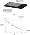
- FIG. 1a is a schematic diagram of a structure in which a plurality of pixel circuits distributed in an array are connected, through a metal conducting wire, to a circuit that includes a driving apparatus for an LED display and a signal driving apparatus of an LED display according to an embodiment of this application.
- the driving apparatus for an LED display includes a temperature sensor (for example, a temperature sensor 201, a temperature sensor 202, ..., and a temperature sensor 20m (m is a positive integer) shown in FIG. 1 ), a control unit 301, and a power supply unit 401.
- the temperature sensor 201, the temperature sensor 202, ..., and the temperature sensor 20m, and the power supply unit 401 are all connected to the control unit 301.
- the power supply unit 401 is further connected to VDDs and VSSs separately corresponding to the plurality of pixel circuits distributed in the array, such as the pixel circuit 101, the pixel circuit 102, ..., and the pixel circuit 10n.
- a specific quantity of temperature sensors is not limited in this application. There may be one or more temperature sensors.
- a first temperature value of the LED display collected by the temperature sensor may represent an average temperature value of at least one pixel circuit in the LED display.
- the plurality of temperature sensors are separately disposed at different positions on the LED display, to separately collect temperature values at the different positions on the LED display, and respectively send the plurality of temperature values that are collected to the control unit 301.
- the two temperature sensors may be respectively disposed at diagonal positions on the LED display.
- the four temperature sensors may be separately disposed at four corners of the LED display.
- N temperature sensors N is a positive integer greater than 4
- the four temperature sensors may be separately disposed at the four corners of the LED display.
- Remaining N - 4 temperature sensors are distributed at a specified interval distance from a temperature sensor at any corner of the LED display.
- a temperature sensor at any corner of the LED display.
- Specific positions of the plurality of temperature sensors are not limited in this application, and may be adjusted based on an actual application.
- the power supply unit 401 provides a driving voltage for a light-emitting diode in each pixel circuit in the LED display. Based on the first temperature value collected by the temperature sensor, the control unit 301 controls the power supply unit 401 to dynamically adjust the driving voltage that is applied to the light-emitting diode in each pixel circuit.
- each pixel circuit includes one light-emitting diode.
- the pixel circuit 101 includes a light-emitting diode 1011
- the pixel circuit 102 includes a light-emitting diode 1021.
- the control unit 301 may determine a target operating voltage corresponding to a first light-emitting diode in a first pixel circuit in the LED display. Then, based on the obtained target operating voltage, the control unit 301 determines a driving voltage that is applied by the power supply unit 401 to the first pixel circuit.
- the preset curve relationship between the temperature value and the operating voltage of the light-emitting diode may be a rule obtained by artificially performing big data analysis and statistics on a large quantity of learned temperature values of displays and operating voltages of light-emitting diodes in pixel circuits in advance.
- the rule is represented through one curve relationship.
- the preset curve relationship between the temperature value and the operating voltage of the light-emitting diode is a linear relationship.
- the first pixel circuit may be any one of the plurality of pixel circuits in the LED display.
- the first pixel circuit is the pixel circuit 101 in FIG. 1 .
- the control unit 301 determines the first temperature value of the LED display based on second temperature values collected by the plurality of temperature sensors. Then, based on the first temperature value and the preset curve relationship between the temperature value and the operating voltage of the light-emitting diode, the control unit 301 determines the target operating voltage corresponding to the first light-emitting diode in the first pixel circuit in the LED display. Then, based on the obtained target operating voltage, the control unit 301 determines the driving voltage that is applied by the power supply unit 401 to the first pixel circuit.
- the first temperature value of the LED display is determined in any one of the following manners.
- a second temperature value of the LED display collected by the temperature sensor 201 is B1.
- a second temperature value of the LED display collected by the temperature sensor 202 is B2.
- a second temperature value of the LED display collected by the temperature sensor 20m is Bm.
- a first temperature value B of the LED display (B1 + B2 + ... + Bm)/m.
- a temperature value obtained through weighted summation of the second temperature values that are respectively collected by the plurality of temperature sensors is C1.
- a second temperature value of the LED display collected by the temperature sensor 201 is C1.
- a second temperature value of the LED display collected by the temperature sensor 202 is C2.
- a second temperature value of the LED display collected by the temperature sensor 20m is Cm.
- a weight value corresponding to the second temperature value C1 is 0.1.
- a weight value corresponding to the second temperature value C2 is 0.3.
- a weight value corresponding to the second temperature value Cm is 0.1.
- a first temperature value C of the LED display C1 ⁇ 0.1 + C2 ⁇ 0.3 + ... + Cm ⁇ 0.1.
- a sum of the weight value corresponding to the second temperature value C1 that is collected by the temperature sensor 201, the weight value corresponding to the second temperature value C2 that is collected by the temperature sensor 202, ..., and the weight value corresponding to the second temperature value Cm that is collected by the temperature sensor 20m is 1.
- control unit 301 may alternatively determine the first temperature value of the LED display in another manner. This is not specifically limited herein in this application.
- FIG. 2 is a schematic diagram of a curve relationship between an operating voltage of a green light LED and a temperature value according to an embodiment of this application.
- a fitting degree R 2 in a linear fitting relationship between the operating voltage of the green light LED and the temperature value is 0.9549.
- the curve relationship is a linear relationship. This is merely an example for description, and a specific type of the curve relationship is not limited in this application.
- the operating voltage of the green light LED decreases by 2.6 mV. In other words, when brightness or displayed content of the green light LED display increases, the temperature value of the green light LED display increases, and correspondingly an operating voltage of the green light LED display decreases.
- a target operating voltage of the green light-emitting diode may be obtained based on the first temperature value and the curve relationship shown in FIG. 2 . Then, a driving voltage applied to a pixel circuit is determined based on a difference between a target operating voltage of the green light-emitting diode at a current moment and a target operating voltage of the green light-emitting diode at a moment before the current moment.
- each pixel circuit generally further includes a positive metal-oxide semiconductor field-effect transistor (Positive metal-oxide semiconductor Field-Effect Transistor, PMOSFET), a storage unit, and a current generation unit.
- PMOSFET Positive metal-oxide semiconductor field-effect transistor
- the pixel circuit 101 shown in FIG. 1 further includes a PMOSFET 1012, a storage unit 1013, and a current generation unit 1014.
- the pixel circuit 102 further includes a PMOSFET 1022, a storage unit 1023, and a current generation unit 1024.
- the pixel circuit 101 is used as an example for description.
- a cathode of the light-emitting diode 1011 is connected to the power supply unit 401 and the ground.
- An anode of the light-emitting diode 1011 is connected to a source of the PMOSFET 1012.
- Agate of the PMOSFET 1012 is connected to the storage unit 1013.
- a drain of the PMOSFET 1012 is connected to the current generation unit 1014.
- the current generation unit 1014 is further connected to the power supply unit 401.
- the storage unit 1013 is configured to store a pulse width modulation (Pulse width modulation, PWM) signal that drives the pixel circuit.
- PWM pulse width modulation
- the current generation unit 1014 is configured to generate a constant current by using a current mirror, to provide the constant current for the pixel circuit.
- the current generation unit 1014 In the pixel circuit 101, after the power supply unit 401 applies a voltage with a specified voltage value to the pixel circuit 101, the current generation unit 1014 generates a constant current I.
- the PMOSFET 1012 controls the constant current I to flow through the light-emitting diode 1011, and uses a duty cycle of the PWM signal stored in the storage unit 1013, to determine conducted time and off time of the PMOSFET 1012. For example, when the duty cycle of the PWM signal is larger, brightness of the light-emitting diode 1011 sensed by a human eye is larger.
- the PMOSFET 1012 may be cut off, to decrease the brightness of the light-emitting diode 1011.
- a specific process of determining the PWM signal stored in the storage unit 1013 is described subsequently. Details are not described herein.
- a difference between a target operating voltage V led-1 of the light-emitting diode 1011 at a current moment and a target operating voltage V led-2 of the light-emitting diode 1011 at a moment before the current moment may be used as a voltage value that needs to be increased by the driving voltage VSS.
- V led-1 of the light-emitting diode 1011 at a current moment a target operating voltage V led-2 of the light-emitting diode 1011 at a moment before the current moment
- VSS driving voltage
- connection manners between the metal-oxide semiconductor field-effect transistors and the light-emitting diodes are different.
- a connection manner between the NMOSFET and the light-emitting diode in the pixel circuit is different from the foregoing described connection manner between the PMOSFET and the light-emitting diode in the pixel circuit.
- the pixel circuit 101 is used as an example for description. FIG.
- FIG. 3 is a schematic diagram of a structure of a specific connection of a pixel circuit 101 that includes an NMOSFET 1015 according to an embodiment of this application.
- An anode of the light-emitting diode 1011 is connected to the power supply unit 401.
- a cathode of the light-emitting diode 1011 is connected to a drain of the NMOSFET 1015.
- a gate of the NMOSFET 1015 is connected to the storage unit 1013 (not shown in FIG. 3 ).
- a source of the NMOSFET 1015 is connected to the current generation unit 1014.
- the current generation unit 1014 is further connected to the power supply unit 401.
- Specific function implementations of the storage unit 1013 and the current generation unit 1014 herein are the same as the specific function implementations of the storage unit 1013 and the current generation unit 1014 when the pixel circuit 101 includes the PMOSFET 1012. Details are not described herein.
- a current I in the pixel circuit 101 is a constant current, and values of V A-Node and VSS remain unchanged, when a value of V led decreases (that is, a value of VDD is decreased), the power of the pixel circuit 101 decreases.
- a difference between a target operating voltage V led-1 of the light-emitting diode 1011 at a current moment and a target operating voltage V led-2 of the light-emitting diode 1011 at a moment before the current moment may be used as a voltage value that needs to be decreased by the driving voltage VDD.
- the driving apparatus for an LED display may further include a first storage unit 501.
- the first storage unit 501 is configured to store an initial VDD and an initial VSS that are applied by the power supply unit 401 to each pixel circuit.
- the control unit 301 controls the power supply unit 401, to adjust the driving voltage that is applied to each pixel circuit to the initial VDD and the initial VSS. Then, the LED display starts to display an image.
- a constituent material of the PMOSFET when the pixel circuit includes the PMOSFET, a constituent material of the PMOSFET may be a silicon metal-oxide semiconductor.
- a constituent material of the NMOSFET when the pixel circuit includes the NMOSFET, a constituent material of the NMOSFET may be a silicon metal-oxide semiconductor.
- the light-emitting diode included in the pixel circuit may alternatively be a micro light-emitting diode (Micro light-emitting diode, Micro LED).
- the pixel circuit When the pixel circuit includes one micro LED, the pixel circuit is combined with the driving apparatus for an LED display, in addition to being applied to a scenario like a television or a notebook with a large display, and may be further applied to a scenario like a wearable augmented reality (augmented reality, AR) with a small display.
- augmented reality augmented reality
- the pixel circuit and the driving apparatus for an LED display are applied to a scenario like a watch, augmented reality display glasses, or virtual reality display glasses with the small display.
- the following describes a process in which the signal driving apparatus of the LED display drives the LED display to display the image.
- the signal driving apparatus of the LED display includes a timing unit 601 and a second storage unit 701.
- the second storage unit 701 stores a to-be-displayed image on the LED display.
- the timing unit 601 in the signal driving apparatus of the LED display is further connected to the control unit 301 in the driving apparatus for an LED display and the storage unit (for example, the storage unit 1013) in each pixel circuit in the LED display.
- the second storage unit 701 in the signal driving apparatus of the LED display is further connected to the control unit 301 in the driving apparatus for an LED display.
- the control unit 301 may further send a timing signal instruction to the timing unit 601.
- the control unit 301 After obtaining the to-be-displayed image of the LED display stored in the second storage unit 701, based on each pixel of the to-be-displayed image of the LED display stored in the second storage unit 701, the control unit 301 generates a pixel data signal corresponding to each pixel. Then, after the timing unit 601 generates the timing signal based on the timing signal instruction, according to a specified operation rule, the control unit 301 separately performs operation on the timing signal and the pixel data signal corresponding to each pixel, to obtain a PWM signal corresponding to a pixel circuit of each pixel.
- the specified operation rule may be an AND operation.
- each pixel circuit After the PWM signal corresponding to each pixel circuit is determined, by using the PWM signal corresponding to each pixel circuit, each pixel circuit adjusts conducted time and off time of a metal-oxide semiconductor field-effect transistor included in the pixel circuit. In this way, the light-emitting diode in the pixel circuit emits light, and finally the LED display displays the image.
- the control unit 301 may perform scanning row by row on each pixel of the to-be-displayed image that is stored in the second storage unit 701 and that is of the LED display. To be specific, pixels are scanned one by one from left to right and from top to bottom, and finally the pixel data signal corresponding to each pixel is generated.
- the timing signal generated by the timing unit 601 is 4 bits, and is represented by pwm0, pwm1, pwm2, and pwm3.
- a duty cycle of a timing signal of the pwm0 is 1/16.
- a duty cycle of a timing signal of the pwm1 is 2/16.
- a duty cycle of a timing signal of the pwm2 is 4/16.
- a duty cycle of a timing signal of the pwm3 is 8/16. If one pixel data signal is 0110, a PWM signal obtained by performing the AND operation on the pixel data signal and the 4-bits timing signal includes pwm 1 and pwm2. That is, a PWM signal in FIG. 4 .
- the 4-bits timing signal may display 15 pieces of gray-scale information. After the operation is performed on the 4-bits timing signal and the pixel data signal, six pieces of gray-scale information may be displayed.
- both the timing signal and the pixel data signal may be in 2 bits to 12 bits.
- the green light LED display includes a plurality of pixel circuits 101
- VDD in each pixel circuit 101 is 1.1 V
- an initial voltage value of VSS is -2.6 V
- the metal-oxide semiconductor field-effect transistor included in each pixel circuit 101 is the PMOSFET.
- the temperature value of the green light LED display is -20°C, according to the rule obtained by performing big data analysis and statistics on a large quantity of learned temperature values of displays and operating voltages of light-emitting diodes in pixel circuits in advance, it is determined that the operating voltage of the green light LED is approximately 2.642 V It can be learned from FIG. 2 that, when the temperature value of the green light LED display increases by 1°C, the operating voltage of the green light LED decreases by 2.6 mV. Therefore, based on the foregoing description, when the temperature value of the green light LED display increases by 1°C, the voltage value of VSS is increased by 2.6 mV correspondingly, to decrease power consumption of the green light LED display. As shown in FIG.
- an embodiment of this application further provides a driving method for the LED display.
- the method may be performed by the control unit 301 in FIG. 1 .
- the method includes the following steps.
- S601 Receive a first temperature value of the LED display collected by a temperature sensor, where the first temperature value represents an average temperature value of at least one pixel circuit in the LED display.
- S602 Control, based on the first temperature value, a power supply unit to dynamically adjust a driving voltage that is applied to a light-emitting diode in each pixel circuit in the LED display.
- each pixel circuit includes the light-emitting diode. Based on the first temperature value and a preset curve relationship between a temperature value and an operating voltage of the light-emitting diode, a target operating voltage corresponding to a first light-emitting diode in a first pixel circuit in the LED display is determined. Based on the target operating voltage, a driving voltage applied by the power supply unit to the first pixel circuit is determined.
- the preset curve relationship between the temperature value and the operating voltage of the light-emitting diode is a linear relationship.
- the target operating voltage of the light-emitting diode 1011 in the pixel circuit 101 in FIG. 1 is first determined based on the first temperature value T and the preset curve relationship between the temperature value and the operating voltage of the light-emitting diode. Then, a driving voltage applied to the pixel circuit 101 is determined based on a difference between a target operating voltage of the light-emitting diode 1011 at a current moment and a target operating voltage of the light-emitting diode 1011 at a moment before the current moment.
- a control code corresponding to the driving voltage is determined based on a pre-constructed correspondence lookup table (Lookup table, LUT) between the driving voltage and the control code (Code).
- the control code corresponding to the driving voltage is input into the power supply unit 401.
- the power supply unit 401 outputs the driving voltage that is applied to the pixel circuit 101.
- the driving voltage herein may be the VDD or the VSS in FIG. 1 .
- the power supply unit 401 may be a power management integrated circuit (Power Management Integrated Circuit, PMIC).
- PMIC Power Management Integrated Circuit
- Table 1 shows a correspondence LUT between control codes and driving voltages.
- the LUT is merely an example. It should be understood that there may be another correspondence between the control code and the driving voltage. This is not limited in this application.
- Table 1 Control code Driving voltage 00001 -4.0 V 00100 -3.2 V 01000 -2.4 V
- the first temperature value is determined based on the second temperature values that are respectively collected by the plurality of temperature sensors. Specifically, includes but is not limited to the following three manners. In other words, this application may further include another manner of determining the first temperature value in addition to the following three manners. This is not exhaustive herein.
- Manner 1 Use a minimum temperature value among the second temperature values that are respectively collected by the plurality of temperature sensors as the first temperature value.
- Manner 2 Use an average value of the second temperature values that are respectively collected by the plurality of temperature sensors as the first temperature value.
- Manner 3 Use a temperature value obtained through weighted summation of the second temperature values that are separately collected by the plurality of temperature sensors as the first temperature value.
- each pixel circuit further includes a positive metal-oxide semiconductor field-effect transistor.
- a cathode of the first light-emitting diode is connected to the power supply unit.
- each pixel circuit further includes a negative metal-oxide semiconductor field-effect transistor.
- An anode of the first light-emitting diode is connected to the power supply unit.
- An embodiment of this application further provides a computer-readable storage medium.
- the computer-readable storage medium stores computer instructions. When the computer instructions are executed, the method in any design of the foregoing driving method for the LED display may be performed.
- An embodiment of this application further provides a computer program product including computer instructions.
- the computer instructions When the computer instructions are executed, the method in any design of the foregoing driving method for the LED display may be performed.
- each aspect of the driving method for the LED display provided in this application may be alternatively implemented in a form of a program product, and the program product includes program code.
- the program code When the program code is run on a computer device or a circuit product, the program code is used to enable the computer device to perform the steps in the driving method for the LED display described in this specification.
- this application may be provided as a method, a system, or a computer program product. Therefore, this application may use a form of hardware only embodiments, software only embodiments, or embodiments with a combination of software and hardware. In addition, this application may be implemented in a form of a computer program product that is implemented on one or more computer-usable storage media (including but not limited to a disk memory, a CD-ROM, an optical memory, and the like) that include computer-usable program code.
- a computer-usable storage media including but not limited to a disk memory, a CD-ROM, an optical memory, and the like
- these computer program instructions may be stored in a computer-readable memory that can indicate a computer or another programmable data processing device to work in a specific manner.
- the instructions stored in the computer-readable memory generate an artifact that includes an instruction apparatus.
- the instruction apparatus implements a specific function in one or more processes in the flowcharts and/or in one or more blocks in the block diagrams.
- these computer program instructions may be loaded onto a computer or another programmable data processing device, so that a series of operations and steps are performed on the computer or the another programmable device, to generate computer-implemented processing. Therefore, the instructions executed on the computer or the another programmable device provide steps for implementing a specific function in one or more processes in the flowcharts and/or in one or more blocks in the block diagrams.
Landscapes
- Engineering & Computer Science (AREA)
- Physics & Mathematics (AREA)
- Computer Hardware Design (AREA)
- General Physics & Mathematics (AREA)
- Theoretical Computer Science (AREA)
- Control Of Indicators Other Than Cathode Ray Tubes (AREA)
- Control Of El Displays (AREA)
Applications Claiming Priority (1)
| Application Number | Priority Date | Filing Date | Title |
|---|---|---|---|
| PCT/CN2021/133769 WO2023092517A1 (zh) | 2021-11-27 | 2021-11-27 | 用于led显示屏的驱动装置、驱动方法及led显示屏 |
Publications (2)
| Publication Number | Publication Date |
|---|---|
| EP4428845A1 true EP4428845A1 (de) | 2024-09-11 |
| EP4428845A4 EP4428845A4 (de) | 2024-09-11 |
Family
ID=86538734
Family Applications (1)
| Application Number | Title | Priority Date | Filing Date |
|---|---|---|---|
| EP21965250.0A Pending EP4428845A4 (de) | 2021-11-27 | 2021-11-27 | Ansteuerungsvorrichtung und ansteuerungsverfahren für led-anzeigebildschirm und led-anzeigebildschirm |
Country Status (4)
| Country | Link |
|---|---|
| US (1) | US20240312398A1 (de) |
| EP (1) | EP4428845A4 (de) |
| CN (1) | CN118284927A (de) |
| WO (1) | WO2023092517A1 (de) |
Families Citing this family (3)
| Publication number | Priority date | Publication date | Assignee | Title |
|---|---|---|---|---|
| US12288511B2 (en) * | 2022-04-01 | 2025-04-29 | X Display Company Technology Limited | Dynamic-voltage control for displays |
| CN118781966A (zh) * | 2023-04-09 | 2024-10-15 | 维信诺科技股份有限公司 | 显示面板的驱动方法、装置和显示设备 |
| WO2025096327A1 (en) * | 2023-10-31 | 2025-05-08 | Google Llc | Temperature-compensated pixel drivers |
Family Cites Families (18)
| Publication number | Priority date | Publication date | Assignee | Title |
|---|---|---|---|---|
| US7656371B2 (en) * | 2003-07-28 | 2010-02-02 | Nichia Corporation | Light emitting apparatus, LED lighting, LED light emitting apparatus, and control method of light emitting apparatus |
| US20050205880A1 (en) * | 2004-03-19 | 2005-09-22 | Aya Anzai | Display device and electronic appliance |
| JP4182930B2 (ja) * | 2004-07-12 | 2008-11-19 | ソニー株式会社 | 表示装置及びバックライト装置 |
| US7492108B2 (en) * | 2005-08-11 | 2009-02-17 | Texas Instruments Incorporated | System and method for driving light-emitting diodes (LEDs) |
| KR20070035388A (ko) * | 2005-09-27 | 2007-03-30 | 엘지전자 주식회사 | 전계발광소자의 전원전압 공급장치 |
| JP2007324493A (ja) * | 2006-06-03 | 2007-12-13 | Nichia Chem Ind Ltd | 発光装置、発光素子駆動回路及び発光素子の駆動方法 |
| KR20080004004A (ko) * | 2006-07-04 | 2008-01-09 | 삼성전자주식회사 | 유기전계 발광표시장치 |
| KR20080008070A (ko) * | 2006-07-19 | 2008-01-23 | 삼성전자주식회사 | 유기발광표시장치 및 이의 구동방법 |
| JP2011076574A (ja) * | 2009-09-30 | 2011-04-14 | Mtec:Kk | 定電流素子 |
| KR20130130434A (ko) * | 2012-05-22 | 2013-12-02 | 엘지디스플레이 주식회사 | 백 라이트 유닛 및 이를 이용한 액정 표시장치 |
| JP6157178B2 (ja) * | 2013-04-01 | 2017-07-05 | ソニーセミコンダクタソリューションズ株式会社 | 表示装置 |
| CN103927989B (zh) * | 2014-04-21 | 2016-09-21 | 中国电子科技集团公司第五十五研究所 | 具有宽温亮度补偿功能的无源有机发光二极管显示装置及亮度补偿方法 |
| CN107195273A (zh) * | 2016-03-14 | 2017-09-22 | 上海和辉光电有限公司 | 一种oled显示器件及改善显示器件显示性能的方法 |
| CN106910461B (zh) * | 2017-05-11 | 2020-12-22 | 京东方科技集团股份有限公司 | 一种显示面板、显示装置及显示驱动方法 |
| CN108182910A (zh) * | 2017-12-21 | 2018-06-19 | 深圳市华星光电技术有限公司 | 一种amoled显示面板的驱动电路及方法、amoled显示面板 |
| CN209249053U (zh) * | 2018-12-27 | 2019-08-13 | 深圳市嘉兴南电科技有限公司 | Led显示屏过温保护电路、装置及led显示屏 |
| CN110839312B (zh) * | 2019-11-27 | 2025-09-16 | 浙江华诺康科技有限公司 | 发光二极管的控制方法、系统、医疗设备和存储介质 |
| CN111445855B (zh) * | 2020-05-11 | 2022-02-25 | 北京集创北方科技股份有限公司 | 驱动电路、显示装置及电子设备 |
-
2021
- 2021-11-27 EP EP21965250.0A patent/EP4428845A4/de active Pending
- 2021-11-27 CN CN202180104338.XA patent/CN118284927A/zh active Pending
- 2021-11-27 WO PCT/CN2021/133769 patent/WO2023092517A1/zh not_active Ceased
-
2024
- 2024-05-24 US US18/674,389 patent/US20240312398A1/en active Pending
Also Published As
| Publication number | Publication date |
|---|---|
| US20240312398A1 (en) | 2024-09-19 |
| CN118284927A (zh) | 2024-07-02 |
| WO2023092517A1 (zh) | 2023-06-01 |
| EP4428845A4 (de) | 2024-09-11 |
Similar Documents
| Publication | Publication Date | Title |
|---|---|---|
| US20240312398A1 (en) | Driving apparatus and driving method for led display, and led display | |
| US11670247B2 (en) | Display panel and method for driving the same, and display device | |
| CN110444152B (zh) | 光学补偿方法及装置、显示装置、显示方法及存储介质 | |
| US12431083B2 (en) | Display panel, method for driving the same, and display apparatus | |
| US9881554B2 (en) | Driving method of pixel circuit and driving device thereof | |
| US11373602B2 (en) | Pixel circuit, method and apparatus for driving the same, array substrate, and display apparatus | |
| WO2019165830A1 (zh) | 用于显示面板的光学补偿方法和光学补偿设备 | |
| EP3098803B1 (de) | Bildverarbeitungsverfahren, bildverarbeitungsschaltung und anzeigevorrichtung mit organischen lichtemittierenden dioden damit | |
| US10146996B2 (en) | Display device configured to compensate luminance based on reflected light | |
| US12148399B2 (en) | Display device and driving method thereof | |
| CN108564919B (zh) | 显示方法、显示控制装置和显示设备 | |
| US8933923B2 (en) | Display device and method for driving display device | |
| CN103021335A (zh) | 一种oled驱动电路、oled显示装置及其亮度调节的方法 | |
| US11164503B2 (en) | Display panel, control method and apparatus thereof, and control device | |
| US11990098B2 (en) | Display brightness control device | |
| US11996046B2 (en) | Display panel and operation method thereof | |
| US11037510B2 (en) | Pixel driving system for AMOLED display device and driving method | |
| US20220093059A1 (en) | Reference Pixel Stressing for Burn-In Compensation Systems and Methods | |
| US20210090500A1 (en) | Driving method of active matrix organic light-emitting diode (amoled) display panel and display device | |
| WO2012132050A1 (ja) | 表示装置、画像処理装置、画像領域検出方法及びコンピュータプログラム | |
| KR102552965B1 (ko) | 모니터용 유기 발광 다이오드 디스플레이 장치 및 그의 영상 처리 방법 | |
| KR20250067892A (ko) | 디스플레이 주변기기의 가변적 밝기 디밍 | |
| CN113077750A (zh) | 一种维持led亮度的方法、驱动电路及显示装置 | |
| KR20170039783A (ko) | 표시 장치의 구동 방법 | |
| KR20250040665A (ko) | 구동 회로, 백라이트 모듈 및 그의 구동 방법, 디스플레이 장치 |
Legal Events
| Date | Code | Title | Description |
|---|---|---|---|
| STAA | Information on the status of an ep patent application or granted ep patent |
Free format text: STATUS: THE INTERNATIONAL PUBLICATION HAS BEEN MADE |
|
| PUAI | Public reference made under article 153(3) epc to a published international application that has entered the european phase |
Free format text: ORIGINAL CODE: 0009012 |
|
| STAA | Information on the status of an ep patent application or granted ep patent |
Free format text: STATUS: REQUEST FOR EXAMINATION WAS MADE |
|
| 17P | Request for examination filed |
Effective date: 20240607 |
|
| A4 | Supplementary search report drawn up and despatched |
Effective date: 20240701 |
|
| AK | Designated contracting states |
Kind code of ref document: A1 Designated state(s): AL AT BE BG CH CY CZ DE DK EE ES FI FR GB GR HR HU IE IS IT LI LT LU LV MC MK MT NL NO PL PT RO RS SE SI SK SM TR |
|
| DAV | Request for validation of the european patent (deleted) | ||
| DAX | Request for extension of the european patent (deleted) | ||
| STAA | Information on the status of an ep patent application or granted ep patent |
Free format text: STATUS: EXAMINATION IS IN PROGRESS |
|
| 17Q | First examination report despatched |
Effective date: 20251201 |