EP4422071A2 - Schaltung mit einer verriegelung mit sätzen von wechselrichtern - Google Patents
Schaltung mit einer verriegelung mit sätzen von wechselrichtern Download PDFInfo
- Publication number
- EP4422071A2 EP4422071A2 EP24163581.2A EP24163581A EP4422071A2 EP 4422071 A2 EP4422071 A2 EP 4422071A2 EP 24163581 A EP24163581 A EP 24163581A EP 4422071 A2 EP4422071 A2 EP 4422071A2
- Authority
- EP
- European Patent Office
- Prior art keywords
- input
- latch
- inverter
- output
- biased
- Prior art date
- Legal status (The legal status is an assumption and is not a legal conclusion. Google has not performed a legal analysis and makes no representation as to the accuracy of the status listed.)
- Granted
Links
Images


Classifications
-
- H—ELECTRICITY
- H03—ELECTRONIC CIRCUITRY
- H03K—PULSE TECHNIQUE
- H03K3/00—Circuits for generating electric pulses; Monostable, bistable or multistable circuits
- H03K3/02—Generators characterised by the type of circuit or by the means used for producing pulses
- H03K3/353—Generators characterised by the type of circuit or by the means used for producing pulses by the use, as active elements, of field-effect transistors with internal or external positive feedback
- H03K3/356—Bistable circuits
- H03K3/356104—Bistable circuits using complementary field-effect transistors
-
- H—ELECTRICITY
- H03—ELECTRONIC CIRCUITRY
- H03K—PULSE TECHNIQUE
- H03K5/00—Manipulating of pulses not covered by one of the other main groups of this subclass
- H03K5/22—Circuits having more than one input and one output for comparing pulses or pulse trains with each other according to input signal characteristics, e.g. slope, integral
- H03K5/24—Circuits having more than one input and one output for comparing pulses or pulse trains with each other according to input signal characteristics, e.g. slope, integral the characteristic being amplitude
- H03K5/2472—Circuits having more than one input and one output for comparing pulses or pulse trains with each other according to input signal characteristics, e.g. slope, integral the characteristic being amplitude using field effect transistors
- H03K5/2481—Circuits having more than one input and one output for comparing pulses or pulse trains with each other according to input signal characteristics, e.g. slope, integral the characteristic being amplitude using field effect transistors with at least one differential stage
-
- H—ELECTRICITY
- H03—ELECTRONIC CIRCUITRY
- H03K—PULSE TECHNIQUE
- H03K3/00—Circuits for generating electric pulses; Monostable, bistable or multistable circuits
- H03K3/02—Generators characterised by the type of circuit or by the means used for producing pulses
- H03K3/353—Generators characterised by the type of circuit or by the means used for producing pulses by the use, as active elements, of field-effect transistors with internal or external positive feedback
- H03K3/356—Bistable circuits
- H03K3/356104—Bistable circuits using complementary field-effect transistors
- H03K3/356113—Bistable circuits using complementary field-effect transistors using additional transistors in the input circuit
- H03K3/35613—Bistable circuits using complementary field-effect transistors using additional transistors in the input circuit the input circuit having a differential configuration
-
- H—ELECTRICITY
- H03—ELECTRONIC CIRCUITRY
- H03K—PULSE TECHNIQUE
- H03K5/00—Manipulating of pulses not covered by one of the other main groups of this subclass
- H03K5/22—Circuits having more than one input and one output for comparing pulses or pulse trains with each other according to input signal characteristics, e.g. slope, integral
- H03K5/24—Circuits having more than one input and one output for comparing pulses or pulse trains with each other according to input signal characteristics, e.g. slope, integral the characteristic being amplitude
- H03K5/2472—Circuits having more than one input and one output for comparing pulses or pulse trains with each other according to input signal characteristics, e.g. slope, integral the characteristic being amplitude using field effect transistors
Definitions
- This invention relates to a circuit with a latch having inverters.
- Latches are used in circuits to store at least momentarily a data state for further utilization.
- latches can be used in circuits such as comparison circuits to momentarily store the final comparison result.
- latch that includes two outputs and two inputs where the outputs latch complementary values indicative of voltages at the latch inputs.
- the latch includes two sets of one or more inverters each coupled in a signal series path. For each set of inverters, the signal input of the first in series inverter is connected to a latch input and the output of the last in series inverter is connected to a latch output.
- the first in series inverters for each set of one or more inverters has a signal input connected to one latch input and a supply voltage input configured to be biased by the other latch input.
- the latch outputs are configured to be set to the same output value state.
- the latch outputs are configured to be latched at complementary output value states dependent upon voltages of the first input and the second input.
- the latch is used in a comparison circuit, where the outputs indicate a result of a comparison of two inputs of the comparison circuit.
- One advantage of providing a latch wherein the first in series inverters have a signal input connected to one of the latch inputs and a supply input coupled to the other latch input is that in some embodiments, the latch changes the state of an output value based on the voltage differential of the two latch inputs passing a particular threshold voltage, thereby allowing for a faster transmission over a latch where the supply input the first in series inverter is coupled to be biased by a supply voltage. Furthermore, during a reset phase, setting the latch outputs to the same output value may be advantageous to provide synchronization for the output data and to avoid inter-symbol interference from previous circuitry that generated the latch input signals.
- FIG. 1 is a circuit diagram of a comparison circuit according to one embodiment of the present invention.
- Comparison circuit 101 includes a pre-amplifier 103, a latch 104, and a latch 105.
- the outputs of latch 105 (VOUT+, VOUT-) provide a latched differential indication of a voltage difference between the inputs of pre-amplifier 103 (VIN+, VIN-).
- comparison circuit 101 operates in three phases: a reset phase, a pre-amplification phase, and a latch phase.
- Pre-amplifier 103 includes two inputs (VIN+, VIN-).
- VIN+ is connected to the signal input of inverter 107 which includes a P-type field effect transistor (PFET) 113 and an N-type field effect transistor (NFET) 111.
- the signal output of inverter 107 is connected to pre-amplifier output VI+.
- VIN- is connected to the signal input of inverter 109 which includes PFET 117 and NFET 115.
- the signal output of inverter 109 is connected to pre-amplifier output VI-.
- the outputs VI+ and VI- are each connected to a terminal of switch 119 that is controlled by signal PHR that is closed during the reset phase to equalize the voltages of VI+ and VI-.
- Signal PHR is provided by a controller 106.
- Pre-amplifier 103 includes two self-biased inverters 125 and 127.
- Inverter 125 includes PFET 131 and NFET 129. The signal input and signal output of inverter 125 are connected to pre-amplifier output VI-.
- Inverter 127 includes PFET 135 and NFET 133. The signal input and signal output of inverter 127 are connected to pre-amplifier output VI+.
- Pre-amplifier 103 includes a latch of two cross coupled inverters 137 and 139.
- Inverter 137 includes PFET 143 and NFET 141.
- the signal input of inverter 137 is connected to VI+ and connected to the signal output of inverter 139.
- Inverter 139 includes PFET 147 and NFET 145.
- the signal input of inverter 139 is connected to VI- and connected to the signal output of inverter 137.
- inverters 107, 109, 125, 127, 137, and 139 are coupled to the high supply voltage terminal VDD through switch 123 that is controlled by the PHPA signal from controller 106.
- the low supply input of inverters 107, 109, 125, 127, 137, and 139 are coupled to the low supply voltage terminal VSS through switch 121 that is controlled by the PHPA signal.
- switch 123 is implemented with a PFET and switch 121 is implemented with an NFET, but these switches can be implemented with other types of switches (e.g., passgates, transmission gates, other types of transistors) in other embodiments.
- Switches 123 and 121 are closed during the pre-amplification phase to provide power to the circuitry of pre-amplifier 103 to bias the high supply nodes (e.g., the high supply inputs of inverters 107, 109, 125, 127, 137, and 139) and the low supply nodes (e.g., the low supply inputs of inverters 107, 109, 125, 127, 137, and 139) at VDD and VSS, respectively.
- switches 123 and 121 are open. See the discussion of Figure 2 below.
- Comparison circuit 101 includes a latch 104 that includes cross coupled inverters 155 and 157.
- inverters 155 and 157 each include a PFET and an NFET (not shown but similar to the latch circuit of inverters 137 and 139).
- the signal input of inverter 155 is connected to a terminal of switch 153, to the output of inverter 157, and to the input VL- of latch 105.
- the input of inverter 157 is connected to a terminal of switch 151, to the output of inverter 155, and to input VL+ of latch 105.
- the other terminal of switch 153 is connected to output VI+ of pre-amplifier 103, and the other terminal of switch 151 is connected to output VI- of pre-amplifier 103.
- switch 153 and switch 151 are implemented with NFETs, but may be implemented with other types of switches (passgates, transmission gates, or other types of transistors such as e.g., PFETs).
- the high supply input of inverter 155 is coupled to the high supply voltage terminal VDD through switch 165, and the low supply terminal of inverter 155 is coupled to the low supply voltage terminal VSS through switch 163.
- the high supply input of inverter 157 is coupled to the high supply voltage terminal VDD through switch 161, and the low supply terminal of inverter 157 is coupled to the low supply voltage terminal VSS through switch 159.
- Switches 165, 163, 161, and 159 are controlled by signal PHL from controller 106 and are conductive during a latching phase and nonconductive during a pre-amplification phase and the reset phase.
- switches 165 and 161 are implemented with PFETs and switches 163 and 159 are implemented with NFETs, but they can be implemented with other types of switches (passgates or other types of transistors) in other embodiments.
- both high supply inputs of inverters 155 and 157 can be coupled to VDD through a single switch and both low supply inputs of inverters 155 and 157 can be coupled to VSS through a single switch.
- Comparison circuit 101 includes a latch 105.
- Latch 105 includes inputs VL+ and VL- that are connected to the outputs of inverter 155 and inverter 157, respectively.
- Latch 105 includes switch 167 that is connected at one terminal to input VL+ and at another terminal to input VL-.
- Switch 167 is controlled by the PHR signal from controller 106 and is conductive (closed) during the reset phase to equalize the voltages of input VL+ and input VL- during the reset phase.
- Switch 167 is open (nonconductive) during the pre-amplification phase and the latching phase.
- Latch 105 includes two sets of inverters with each set coupled in a signal series path between a latch input and latch output.
- One set includes inverters 183 and 185 where the signal input of first in series inverter 183 is connected to latch input VL+ and the signal output of last in series inverter 185 is connected to latch output VOUT+.
- the signal output of inverter 183 is connected to the signal input of inverter 185.
- Inverter 183 includes a PFET 189 whose source (the high supply input of inverter 183) is connected to high supply voltage terminal VDD and whose drain is connected to the drain of NFET 187 and the signal output of inverter 183.
- Inverter 183 includes NFET 187 whose gate is connected to the gate of PFET 189 and to latch input VL+ at the signal input of inverter 183.
- the source of NFET 187 (the low supply input of inverter 183) is connected to latch input VL- such that the low supply input of inverter 183 is biased by latch input VL-.
- Inverter 185 includes PFET 193 and NFET 191.
- the gates of PFET 193 and NFET 191 are connected at the signal input of inverter 185 to the signal output of inverter 183.
- the high supply input of inverter 185 (the source of PFET 193) is connected to high supply voltage terminal VDD and the low supply input of inverter 185 (the source of NFET 191) is connected to the low supply voltage terminal VSS.
- the drains of PFET 193 and NFET 191 are connected at the signal output of inverter 185 to latch output VOUT+.
- Inverter 171 includes a PFET 177 whose source (the high supply input of inverter 171) is connected to high supply voltage terminal VDD and whose drain is connected to the drain of NFET 175 and to the signal output of inverter 171.
- Inverter 171 includes NFET 175 whose gate is connected to the gate of PFET 177 and to latch input VL- at the signal input of inverter 171.
- the source of NFET 175 (the low supply input of inverter 171) is connected to latch input VL+ such that the low supply input of inverter 171 is biased by latch input VL+.
- Inverter 173 includes PFET 181 and NFET 179.
- the gates of PFET 181 and NFET 179 are connected at the signal input of inverter 173 to the signal output of inverter 171.
- the high supply input of inverter 173 (the source of PFET 181) is connected to high supply voltage terminal VDD and the low supply input of inverter 173 (the source of NFET 179) is connected to the low supply voltage terminal VSS.
- the drains of PFET 181 and NFET 179 are connected at the signal output of inverter 173 to latch output VOUT-.
- the VDD high supply voltage terminal is biased at .8V and the VSS low supply voltage terminal is biased at a ground voltage.
- these supply voltage terminals may be biased at other supply voltages including negative voltages for VSS.
- a comparison circuit may have other configurations, include other circuitry and/or operate in other modes.
- some embodiments e.g., embodiments with high input voltages
- the inverters of Figure 1 are shown being implemented with a P-type transistor (e.g., a PFET) in series with an N-type transistor (e.g., and NFET), at least some of the inverters of Figure 1 may be implemented with other inverter configurations in other embodiments.
- pre-amplifier 103 may have other configurations in other embodiments.
- Circuit 101 may be implemented with other types of transistors in other embodiments (e.g., bipolar).
- FIG. 2 is a timing diagram showing voltages of comparison circuit 101 during operation according to one embodiment of the present invention.
- comparison circuit 101 operates in three phases: a reset phase (PHR), a pre-amplification (“pre-amp”) phase (PHPA), and a latch phase (PHL). These sequential phases are repeatedly performed to provide a differential indication at VOUT+ and VOUT- of a comparison of the voltage of VIN+ with the voltage of VIN+.
- Controller 106 controls the timing of the phases.
- the PHR signal is asserted to close switch 119 to equalize the voltages of VI+ and VI- at the common mode voltage of VI+ and VI-during the previous latch phase.
- the PHR signal being asserted also closes switch 167 to equalize the voltages of VL+ and VL- at the common mode voltage (VCM) of VL+ and VL- during the previous latch phase. Because VL+ and VL- are equalized during the reset phase, the gate-to-source voltages (VGS) of NFETs 187 and 175 are at 0V.
- the PHPA signal is non asserted such that switches 151 and 153 are open to isolate VI+ and VI- from latch 104.
- the PHPA signal being in a nonconductive state during the reset phase also opens switches 123 and 121 so that the inverters of pre-amplifier 103 are not biased at their supply voltage inputs by high supply voltage terminal VDD and low supply voltage terminal VSS.
- none of the transistors of the inverters of pre-amplifier 103 can pull the voltages of either output VI+ or VI- away form the common mode voltage.
- the PHL signal is non asserted such that switches 159, 161, 163, and 165 are nonconductive so that inverters 157 and 155 are not biased by supply voltages VDD and VSS.
- inverters 157 and 155 cannot pull the voltages of latch inputs VL+ and VL- from the common mode voltage.
- the threshold voltages of PFETs 189 and 177 are less than the voltage difference between VDD and the common mode voltages of VL+ and VL- such that PFETs 189 and 177 will be conductive during the reset phase. With PFETs 189 and 177 being conductive, NFETs 191 and 179 are conductive to pull the voltages of VOUT+ and VOUT-, respectively, to VSS.
- PFETs 189 and 177 have a threshold voltage of .3V such that they are both conductive in the reset phase.
- NFETs 175 and 187 also have a threshold voltage of .3V, but these threshold voltages may be of other values in other embodiments.
- switches 121 and 123 are closed to bias the low supply voltage nodes of pre-amplifier 103 at VSS and bias the high supply voltage nodes of pre-amplifier 103 at VDD.
- Switch 119 is open so that Vi+ and VI- are no longer equalized.
- Switches 151 and 153 are closed and switch 167 is open.
- VIN+ is at a higher voltage than VIN- which causes VL+ to increase and VL- to decrease during the pre-amplification phase.
- inverters 125 and 127 act to pull VIand VI+ to the threshold voltage of inverters 125 and 127, respectfully, which is designed to be approximately the common mode voltage of VIN+ and VIN-.
- Self-biased inverters 125 and 127 act to reduce the common mode sensitivity of pre-amplifier 103, but they also reduce the gain of the pre-amplifier 103.
- Cross coupled inverters 137 and 139 act to enhance the rate of increase of the voltage difference between VI- and VI+ (and between VL+ and VL-) (i.e., increase the gain of pre-amplifier 103) for the given amount of transistor current.
- the transistors of inverters 137 and 139 are stronger than the transistors of inverters 125 and 127 so as to overcome the effect of self-biased inverters 125 and 127.
- the size of the transistors of inverters 125, 127, 137 and 139 can be adjusted to tailor the gain versus the common mode sensitivity of pre-amplifier 103.
- pre-amplifier 103 includes only one set of internal signal nodes (VI-, VI+), the speed of pre-amplifier 103 is greater than with a pre-amplifier with multiple sets of nodes.
- switches 151 and 153 are open to isolate VI+ and VI- from VL- and VL+, respectively. Also, switches 123 and 121 are open so that the supply nodes of the inverters of pre-amplifier 103 are unbiased.
- switches 159, 161, 163, and 165 are closed so that the high supply inputs of inverters 155 and 157 are biased at VDD and the low supply inputs of inverters 155 and 157 are biased at VSS. Because the cross coupled inverters 155 and 157 are powered during the latch phase, the voltage difference between VL+ and VL- increases at a higher rate. As shown in Figure 2 , the voltage of VL+ rises at a faster rate and the voltage of VL- falls at a faster rate during the latch phase.
- the latch outputs (VOUT+. VOUT-) will change state when the voltage difference between the latch inputs exceeds the threshold voltage of one of NFETs 187 and 175, depending upon which latch input has the higher voltage.
- FIG. 2 shows a gate-to-source voltage of NFET 187 (VGS NFET 187), which is the voltage of VL+ minus the voltage of VL-.
- Figure 2 also shows a gate-to-source voltage of NFET 175 (VGS NFET 175), which is the voltage of VL- minus the voltage of VL+.
- VGS NFET 187 and 175 are at 0V during the reset phase in that VL+ and VL- are equalized at the same voltage.
- VGS gate-to-source voltages
- NFET 187 or NFET 175 has a positive VGS that surpasses its threshold, that NFET becomes conductive to make the PFET (193 or 181) of the subsequent inverter (185 or 173) conductive to pull VOUT+ or VOUT- to a high voltage state.
- the NFET (189 or 177) with a negative VGS remains nonconductive where its corresponding latch output (VOUT+, VOUT-) does not change.
- NFET 187 becomes conductive when its gate-to-source volage (VGS) rises above its threshold voltage (e.g..3V in some embodiments). This happens when VL+ minus VL- is greater than the threshold voltage of NFET 187. NFET 187 becoming conductive pulls makes PFET 193 to pull its corresponding latch output VOUT+ to a high voltage state of VDD, whereas VOUT- is remains as its low voltage state of VSS.
- VGS gate-to-source volage
- VL+ continues to rise and VL- continues to fall until VL+ reaches VDD and VL- reaches VSS.
- VGS NFET 187 represents the voltage of VL+ minus the voltage of VL-, it rises to VDD at twice the rate as VL+ rises to VDD.
- VGS NFET 175 represents the voltage of VL- minus the voltage of VL+, it falls to -VDD at twice the rate as VL- falls to VSS.
- NFETs 187 and 175 are biased by the other latch input that is not applied to its signal input, their gate-to-source voltages will change at twice the rate as the latch input voltages applied to their signal inputs due to the diverging directions of the voltages of the latch inputs (VL+, VL-). Accordingly, the NFETs will turn on faster than if the sources of each NFET were biased at VSS, thereby providing for a faster latch and a faster comparison circuit.
- switches 159, 161, 163, and 165 open so that inverters 157 and 155 are unbiased.
- Switch 119 is at a closed state to equalize the voltages on VI+ and VI- to their common mode voltage.
- Switch 167 is closed to equalize the voltages of VL+ and VL- to their common mode voltage (VCM). Due to the equalization of the voltages of VL+ and VL-, the gate-to-source voltage of NFETs 187 and 175 return to 0 volts. As shown in Figure 2 , when the gate-to-source voltage of NFET 187 falls past its threshold voltage, VOUT+ returns to its low voltage state.
- comparison circuit 101 includes two outputs (VOUT+ and VOUT-) that during a reset phase at are at the same low voltage state and during a latch phase are at complementary voltage states depending upon whether VIN+ or VIN- is at a higher voltage with respect to each other. With such an embodiment, only one latch output is required to change state to indicate a volage comparison result during the latch phase. In other embodiments, comparison circuit may have a different number of phases.
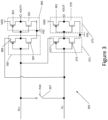
- FIG 3 is a circuit diagram of another latch 305 according to an embodiment of the present invention.
- Latch 305 is similar to latch 105 of Figure 1 except that the high supply inputs (the sources of PFETs 389 and 377) of the first in series inverters (383 and 371) are connected to the opposing latch input (VL- and VL+, respectively) and the low supply inputs (the sources of NFETs 387 and 375) of the first in series inverters (383 and 371) are connected to VSS.
- the signal input of inverter 383 is connected to latch input VL+ and the signal input of inverter 371 is connected to latch input VL-.
- Latch 305 includes a switch 367 for equalizing the latch inputs VL+ and VL- during a reset phase.
- the signal output of inverter 383 is connected to the signal input of inverter 385, which includes PFET 393 and NFET 391.
- the signal output of inverter 371 is connected to the signal input of inverter 373, which includes PFET 381 and 379.
- NFETs 387 and 375 have a threshold voltage that is less than the common mode voltage of VL+ and VL-. Thus, when VL+ and VL- are at the common mode voltage, NFETs 387 and 375 are conductive so that VOUT+ and VOUT- are both at a high voltage state. As the voltages of VL+ and VL- diverge in the latch phase, either PFET 389 or PFET 377 will become conductive when its gate-to-source voltage falls below its threshold voltage (or its source-to-gate threshold rises above its threshold voltage).
- each set of inverters can have more than two inverters in the signal path such that the reset voltage state of VOUT+ and VOUT-can be at VSS.
- Comparison circuit 101 can be used to provide a comparison of two input voltages in a variety of systems such as e.g., memories, serial interfaces, data converters, computational hardware, and ADCs.
- comparison circuit 101 may be used in a successive approximation register (SAR) analog to digital converter (ADC) where the relatively high speed of comparison circuit 101 and large differential gain may be beneficial for achieving high clock speeds and high resolution.
- SAR successive approximation register
- ADC analog to digital converter
- such a comparison circuit may be beneficial for high frequency applications (e.g., 5 GHz or greater) such as with 5G/6G implementations and other wireless systems or with auto radar systems, and in serializer and deserializer (SerDes) applications.
- SerDes serializer and deserializer
- the gain of pre-amplifier 103 may be large enough that latch 104 is not needed.
- the input inverters 107 and 109 can be relatively small in size, thereby providing for a small input capacitance and lower noise.
- the comparison circuit can be optimized for a wide range of frequencies without modifying the design by adjusting the length of the pre-amplification phase.
- each set of one or more inverters may have only one inverter in the signal path or may have more than two inverters in the signal path.
- One advantage of a set having two or more inverters in a signal path is that the latch outputs (VOUT+ and VOUT-) may transition faster to well-defined complementary digital output states based a relatively small differential latch input voltages around a common mode.
- a source or a drain is a current terminal for a FET (field effect transistor).
- a gate is a control terminal for a FET.
- Two devices can be "coupled” to each other either through other devices or by being connected to each other.
- Latch inputs VL+ and VL- are coupled through switch 167.
- Latch input VL+ is also coupled to the gate to PFET 189 by being connected to the gate of PFET 189.
- a circuit in one embodiment, includes a latch.
- the latch includes a first input, a second input, a first output, a second output, and a first set of one or more inverters coupled in a signal series path.
- a signal input of a first in series invertor of the first set is connected to the first input and a signal output of a last in series inverter of the first set is connected to the first output.
- the first in series inverter of the first set includes a first supply input that is configured to be biased by the second input.
- the latch includes a second set of one or more inverters coupled in a signal series path.
- a signal input of a first in series inverter of the second set is connected to the second input and a signal output of a last in series inverter of the second set is connected to the second output.
- the first in series inverter of the second set includes a first supply input that is configured to be biased by the first input.
- the first output and the second output are configured to be set to a same output value state.
- the first output and the second output are configured to be latched at complementary output value states dependent upon voltages of the first input and the second input.
- Another embodiment includes a method for comparing a voltage of a first input of a pre-amplifier and a voltage of a second input of the pre-amplifier.
- the method includes during a reset phase controlling a first switch to be in a conductive state to equalize a first output of the pre-amplifier and a second output of the pre-amplifier, and controlling to be in a nonconductive state, a second switch coupled at one terminal to the first output of the pre-amplifier and coupled at a second terminal to a first signal input of a set of cross coupled inverters.
- a third switch coupled at one terminal to the second output of the pre-amplifier and coupled at a second terminal to a second signal input of a set of cross coupled inverters.
- a fourth switch coupled a one terminal to a first input of a latch and coupled to a second input of the latch.
- the latch includes a first output, a second output.
- the latch includes a first set of one or more inverters coupled in a signal series path, wherein a signal input of a first in series invertor of the first set is connected to the first input of the latch and a signal output of a last in series inverter of the first set is connected to the first output of the latch, wherein the first in series inverter of the first set includes a first supply input that is coupled to the second input of the latch to be biased by the second input of the latch.
- the latch includes a second set of one or more inverters coupled in a signal series path, wherein a signal input of a first in series invertor of the second set is connected to the second input of the latch and a signal output of the last in series inverter of the second set is connected to the second output of the latch, wherein the first in series inverter of the second set includes a first supply input that is coupled to the first input of the latch to be biased by the first input of the latch.
- the first output of the latch and the second output of the latch are each at a first voltage state.
- a pre-amplification phase controlling the first switch to be in a nonconductive state, controlling the second switch and the third switch to be in a conductive state, and controlling the fourth switch to be in a nonconductive state.
- controlling the second switch and the third switch controlling the nonconductive state.
- the first output and the second output of the latch circuit are each in a complementary state to each other to indicate a comparison result of the voltage of the first input of the pre-amplifier with the voltage of the second input of the pre-amplifier.
- during the reset phase controlling a biasing of high supply voltage nodes of the pre-amplifier to be in an unbiased condition; controlling a biasing of low supply voltage nodes of the pre-amplifier to be in an unbiased condition; during the pre-amplification phase: biasing the high supply voltage nodes of the pre-amplifier at a high supply voltage; biasing the low supply voltage nodes of the pre-amplifier at a low supply voltage.
- a comparison circuit in another embodiment, includes a pre-amplifier including a first input, a second input, a first output, a second output, and a first switch coupled between the first output and the second output, wherein when the first switch is conductive, a voltage of the first output and a voltage of the second output are equalized.
- the comparison circuit includes a set of cross coupled inverters including a first signal input coupled to the first output of the pre-amplifier by a second switch, a second signal input coupled to the second output of the pre-amplifier by a third switch, a first signal output, and a second signal output.
- the comparison circuit includes a latch including a first input coupled to the first signal output of the set of cross coupled inverters, a second input coupled to the second signal output of the set of cross coupled inverters and a fourth switch coupled between the first input of the latch and the second input of the latch, wherein when the fourth switch is conductive, a voltage of the first input of the latch and a voltage of the second input of the latch are equalized.
- the latch includes a first latch output, a second latch output, and a first set of one or more inverters coupled in a signal series path, wherein a signal input of a first in series invertor of the first set is connected to the first input of the latch and a signal output of a last in series inverter of the first set is connected to the first latch output, wherein the first in series inverter of the first set includes a first supply input that is coupled to the second input of the latch to be biased by the second input of the latch.
- the latch includes a second set of one or more inverters coupled in a signal series path, wherein a signal input of a first in series invertor of the second set is connected to the second input of the latch and a signal output of a last in series inverter of the second set is connected to the second latch output, wherein the first in series inverter of the second set includes a first supply input that is coupled to the first input of the latch to be biased by the first input of the latch.
- the first latch output and the second latch output are latched at complementary output value states indicative of a comparison of voltages of the first input of the pre-amplifier and the second input of the pre-amplifier.
- the first switch and the fourth switch are configured to be conductive; the second switch and the third switch are configured to be nonconductive; high supply voltage nodes and low supply voltage nodes of the set of cross coupled inverters are configured to be unbiased; high supply voltage nodes and low supply voltage nodes of the pre-amplifier are configured to be unbiased.
Landscapes
- Physics & Mathematics (AREA)
- Nonlinear Science (AREA)
- Manipulation Of Pulses (AREA)
- Measurement Of Current Or Voltage (AREA)
Priority Applications (3)
| Application Number | Priority Date | Filing Date | Title |
|---|---|---|---|
| EP24163581.2A EP4422071B1 (de) | 2024-03-14 | 2024-03-14 | Schaltung mit einem latch mit sätzen von invertern |
| US19/071,028 US20250293678A1 (en) | 2024-03-14 | 2025-03-05 | Circuit with a latch having sets of inverters |
| CN202510265107.7A CN120658234A (zh) | 2024-03-14 | 2025-03-07 | 具有带多组反相器的锁存器的电路 |
Applications Claiming Priority (1)
| Application Number | Priority Date | Filing Date | Title |
|---|---|---|---|
| EP24163581.2A EP4422071B1 (de) | 2024-03-14 | 2024-03-14 | Schaltung mit einem latch mit sätzen von invertern |
Publications (3)
| Publication Number | Publication Date |
|---|---|
| EP4422071A2 true EP4422071A2 (de) | 2024-08-28 |
| EP4422071A3 EP4422071A3 (de) | 2024-10-30 |
| EP4422071B1 EP4422071B1 (de) | 2026-03-11 |
Family
ID=90365625
Family Applications (1)
| Application Number | Title | Priority Date | Filing Date |
|---|---|---|---|
| EP24163581.2A Active EP4422071B1 (de) | 2024-03-14 | 2024-03-14 | Schaltung mit einem latch mit sätzen von invertern |
Country Status (3)
| Country | Link |
|---|---|
| US (1) | US20250293678A1 (de) |
| EP (1) | EP4422071B1 (de) |
| CN (1) | CN120658234A (de) |
Family Cites Families (2)
| Publication number | Priority date | Publication date | Assignee | Title |
|---|---|---|---|---|
| WO2010064338A1 (ja) * | 2008-12-02 | 2010-06-10 | パナソニック株式会社 | 比較器およびa/d変換器 |
| CN112636727A (zh) * | 2019-10-08 | 2021-04-09 | 长鑫存储技术有限公司 | 数据的存储比较方法、存储比较电路装置及半导体存储器 |
-
2024
- 2024-03-14 EP EP24163581.2A patent/EP4422071B1/de active Active
-
2025
- 2025-03-05 US US19/071,028 patent/US20250293678A1/en active Pending
- 2025-03-07 CN CN202510265107.7A patent/CN120658234A/zh active Pending
Also Published As
| Publication number | Publication date |
|---|---|
| EP4422071A3 (de) | 2024-10-30 |
| US20250293678A1 (en) | 2025-09-18 |
| CN120658234A (zh) | 2025-09-16 |
| EP4422071B1 (de) | 2026-03-11 |
Similar Documents
| Publication | Publication Date | Title |
|---|---|---|
| EP1058385B1 (de) | Komparatorschaltung | |
| WO2009003068A1 (en) | Level shifter having low duty cycle distortion | |
| US11295789B2 (en) | Latching sense amplifier | |
| US6392449B1 (en) | High-speed low-power low-offset hybrid comparator | |
| US20040155689A1 (en) | Differential input receiver with hysteresis | |
| CN113196660B (zh) | 用于功率和高速应用的比较器 | |
| US9654088B2 (en) | Hysteresis circuit | |
| US20070247228A1 (en) | Apparatus for receiver equalization | |
| US20120268185A1 (en) | Comparator with adaptive timing | |
| GB2381971A (en) | Rail-to-rail CMOS comparator | |
| US8482317B2 (en) | Comparator and method with adjustable speed and power consumption | |
| US6211712B1 (en) | CMOS comparator with hysteresis | |
| EP4422071A2 (de) | Schaltung mit einer verriegelung mit sätzen von wechselrichtern | |
| EP1352472A1 (de) | Schaltung zum empfangen und ansteuern eines taktsignals | |
| CN115225065A (zh) | 时钟调整电路 | |
| CN111600607B (zh) | 一种宽带低功耗比较器电路 | |
| KR101055788B1 (ko) | 광대역의 공통모드 입력전압 범위를 가지는 차동 증폭회로 및 그 차동 증폭회로를 구비한 입력 버퍼 | |
| EP4169161A1 (de) | Differenzaktivierte verriegelung für gan-basierten pegelschieber | |
| US6304107B1 (en) | Comparator metastability performance from an enhanced comparator detection circuit | |
| US6448822B1 (en) | Comparator for negative and near-ground signals | |
| US20200244256A1 (en) | Low-Power Sense Amplifier | |
| US20020158685A1 (en) | Differential amplifying circuit and multi-stage differential amplifying circuit using the same | |
| US12483244B2 (en) | Buffer with reduced shoot-through current | |
| US11063580B2 (en) | Input buffer with wide range of I/O voltage level | |
| KR20250155889A (ko) | 빠른 속도와 높은 에너지 효율을 갖는 비교기 |
Legal Events
| Date | Code | Title | Description |
|---|---|---|---|
| PUAI | Public reference made under article 153(3) epc to a published international application that has entered the european phase |
Free format text: ORIGINAL CODE: 0009012 |
|
| STAA | Information on the status of an ep patent application or granted ep patent |
Free format text: STATUS: THE APPLICATION HAS BEEN PUBLISHED |
|
| AK | Designated contracting states |
Kind code of ref document: A2 Designated state(s): AL AT BE BG CH CY CZ DE DK EE ES FI FR GB GR HR HU IE IS IT LI LT LU LV MC ME MK MT NL NO PL PT RO RS SE SI SK SM TR |
|
| PUAL | Search report despatched |
Free format text: ORIGINAL CODE: 0009013 |
|
| AK | Designated contracting states |
Kind code of ref document: A3 Designated state(s): AL AT BE BG CH CY CZ DE DK EE ES FI FR GB GR HR HU IE IS IT LI LT LU LV MC ME MK MT NL NO PL PT RO RS SE SI SK SM TR |
|
| RIC1 | Information provided on ipc code assigned before grant |
Ipc: H03K 5/24 20060101ALI20240924BHEP Ipc: H03K 3/356 20060101AFI20240924BHEP |
|
| STAA | Information on the status of an ep patent application or granted ep patent |
Free format text: STATUS: REQUEST FOR EXAMINATION WAS MADE |
|
| 17P | Request for examination filed |
Effective date: 20250430 |
|
| GRAP | Despatch of communication of intention to grant a patent |
Free format text: ORIGINAL CODE: EPIDOSNIGR1 |
|
| STAA | Information on the status of an ep patent application or granted ep patent |
Free format text: STATUS: GRANT OF PATENT IS INTENDED |
|
| INTG | Intention to grant announced |
Effective date: 20251007 |
|
| RAP1 | Party data changed (applicant data changed or rights of an application transferred) |
Owner name: NXP B.V. |
|
| GRAS | Grant fee paid |
Free format text: ORIGINAL CODE: EPIDOSNIGR3 |
|
| GRAA | (expected) grant |
Free format text: ORIGINAL CODE: 0009210 |
|
| STAA | Information on the status of an ep patent application or granted ep patent |
Free format text: STATUS: THE PATENT HAS BEEN GRANTED |
|
| AK | Designated contracting states |
Kind code of ref document: B1 Designated state(s): AL AT BE BG CH CY CZ DE DK EE ES FI FR GB GR HR HU IE IS IT LI LT LU LV MC ME MK MT NL NO PL PT RO RS SE SI SK SM TR |
|
| REG | Reference to a national code |
Ref country code: CH Ref legal event code: F10 Free format text: ST27 STATUS EVENT CODE: U-0-0-F10-F00 (AS PROVIDED BY THE NATIONAL OFFICE) Effective date: 20260311 Ref country code: GB Ref legal event code: FG4D |
|
| REG | Reference to a national code |
Ref country code: DE Ref legal event code: R096 Ref document number: 602024003052 Country of ref document: DE |
|
| REG | Reference to a national code |
Ref country code: IE Ref legal event code: FG4D |
|
| PGFP | Annual fee paid to national office [announced via postgrant information from national office to epo] |
Ref country code: AT Payment date: 20260312 Year of fee payment: 3 |