EP4421790A1 - Pixelschaltung, anzeigetafel, ansteuerungsverfahren und anzeigevorrichtung - Google Patents
Pixelschaltung, anzeigetafel, ansteuerungsverfahren und anzeigevorrichtung Download PDFInfo
- Publication number
- EP4421790A1 EP4421790A1 EP22944165.4A EP22944165A EP4421790A1 EP 4421790 A1 EP4421790 A1 EP 4421790A1 EP 22944165 A EP22944165 A EP 22944165A EP 4421790 A1 EP4421790 A1 EP 4421790A1
- Authority
- EP
- European Patent Office
- Prior art keywords
- terminal
- control
- circuit
- electrically connected
- transistor
- Prior art date
- Legal status (The legal status is an assumption and is not a legal conclusion. Google has not performed a legal analysis and makes no representation as to the accuracy of the status listed.)
- Pending
Links
Images






Classifications
-
- G—PHYSICS
- G09—EDUCATION; CRYPTOGRAPHY; DISPLAY; ADVERTISING; SEALS
- G09G—ARRANGEMENTS OR CIRCUITS FOR CONTROL OF INDICATING DEVICES USING STATIC MEANS TO PRESENT VARIABLE INFORMATION
- G09G3/00—Control arrangements or circuits, of interest only in connection with visual indicators other than cathode-ray tubes
- G09G3/20—Control arrangements or circuits, of interest only in connection with visual indicators other than cathode-ray tubes for presentation of an assembly of a number of characters, e.g. a page, by composing the assembly by combination of individual elements arranged in a matrix no fixed position being assigned to or needed to be assigned to the individual characters or partial characters
- G09G3/22—Control arrangements or circuits, of interest only in connection with visual indicators other than cathode-ray tubes for presentation of an assembly of a number of characters, e.g. a page, by composing the assembly by combination of individual elements arranged in a matrix no fixed position being assigned to or needed to be assigned to the individual characters or partial characters using controlled light sources
- G09G3/30—Control arrangements or circuits, of interest only in connection with visual indicators other than cathode-ray tubes for presentation of an assembly of a number of characters, e.g. a page, by composing the assembly by combination of individual elements arranged in a matrix no fixed position being assigned to or needed to be assigned to the individual characters or partial characters using controlled light sources using electroluminescent panels
- G09G3/32—Control arrangements or circuits, of interest only in connection with visual indicators other than cathode-ray tubes for presentation of an assembly of a number of characters, e.g. a page, by composing the assembly by combination of individual elements arranged in a matrix no fixed position being assigned to or needed to be assigned to the individual characters or partial characters using controlled light sources using electroluminescent panels semiconductive, e.g. using light-emitting diodes [LED]
- G09G3/3208—Control arrangements or circuits, of interest only in connection with visual indicators other than cathode-ray tubes for presentation of an assembly of a number of characters, e.g. a page, by composing the assembly by combination of individual elements arranged in a matrix no fixed position being assigned to or needed to be assigned to the individual characters or partial characters using controlled light sources using electroluminescent panels semiconductive, e.g. using light-emitting diodes [LED] organic, e.g. using organic light-emitting diodes [OLED]
-
- G—PHYSICS
- G09—EDUCATION; CRYPTOGRAPHY; DISPLAY; ADVERTISING; SEALS
- G09G—ARRANGEMENTS OR CIRCUITS FOR CONTROL OF INDICATING DEVICES USING STATIC MEANS TO PRESENT VARIABLE INFORMATION
- G09G3/00—Control arrangements or circuits, of interest only in connection with visual indicators other than cathode-ray tubes
- G09G3/20—Control arrangements or circuits, of interest only in connection with visual indicators other than cathode-ray tubes for presentation of an assembly of a number of characters, e.g. a page, by composing the assembly by combination of individual elements arranged in a matrix no fixed position being assigned to or needed to be assigned to the individual characters or partial characters
- G09G3/22—Control arrangements or circuits, of interest only in connection with visual indicators other than cathode-ray tubes for presentation of an assembly of a number of characters, e.g. a page, by composing the assembly by combination of individual elements arranged in a matrix no fixed position being assigned to or needed to be assigned to the individual characters or partial characters using controlled light sources
- G09G3/30—Control arrangements or circuits, of interest only in connection with visual indicators other than cathode-ray tubes for presentation of an assembly of a number of characters, e.g. a page, by composing the assembly by combination of individual elements arranged in a matrix no fixed position being assigned to or needed to be assigned to the individual characters or partial characters using controlled light sources using electroluminescent panels
- G09G3/32—Control arrangements or circuits, of interest only in connection with visual indicators other than cathode-ray tubes for presentation of an assembly of a number of characters, e.g. a page, by composing the assembly by combination of individual elements arranged in a matrix no fixed position being assigned to or needed to be assigned to the individual characters or partial characters using controlled light sources using electroluminescent panels semiconductive, e.g. using light-emitting diodes [LED]
- G09G3/3208—Control arrangements or circuits, of interest only in connection with visual indicators other than cathode-ray tubes for presentation of an assembly of a number of characters, e.g. a page, by composing the assembly by combination of individual elements arranged in a matrix no fixed position being assigned to or needed to be assigned to the individual characters or partial characters using controlled light sources using electroluminescent panels semiconductive, e.g. using light-emitting diodes [LED] organic, e.g. using organic light-emitting diodes [OLED]
- G09G3/3225—Control arrangements or circuits, of interest only in connection with visual indicators other than cathode-ray tubes for presentation of an assembly of a number of characters, e.g. a page, by composing the assembly by combination of individual elements arranged in a matrix no fixed position being assigned to or needed to be assigned to the individual characters or partial characters using controlled light sources using electroluminescent panels semiconductive, e.g. using light-emitting diodes [LED] organic, e.g. using organic light-emitting diodes [OLED] using an active matrix
- G09G3/3233—Control arrangements or circuits, of interest only in connection with visual indicators other than cathode-ray tubes for presentation of an assembly of a number of characters, e.g. a page, by composing the assembly by combination of individual elements arranged in a matrix no fixed position being assigned to or needed to be assigned to the individual characters or partial characters using controlled light sources using electroluminescent panels semiconductive, e.g. using light-emitting diodes [LED] organic, e.g. using organic light-emitting diodes [OLED] using an active matrix with pixel circuitry controlling the current through the light-emitting element
-
- G—PHYSICS
- G09—EDUCATION; CRYPTOGRAPHY; DISPLAY; ADVERTISING; SEALS
- G09G—ARRANGEMENTS OR CIRCUITS FOR CONTROL OF INDICATING DEVICES USING STATIC MEANS TO PRESENT VARIABLE INFORMATION
- G09G2300/00—Aspects of the constitution of display devices
- G09G2300/04—Structural and physical details of display devices
- G09G2300/0421—Structural details of the set of electrodes
- G09G2300/0426—Layout of electrodes and connections
-
- G—PHYSICS
- G09—EDUCATION; CRYPTOGRAPHY; DISPLAY; ADVERTISING; SEALS
- G09G—ARRANGEMENTS OR CIRCUITS FOR CONTROL OF INDICATING DEVICES USING STATIC MEANS TO PRESENT VARIABLE INFORMATION
- G09G2300/00—Aspects of the constitution of display devices
- G09G2300/08—Active matrix structure, i.e. with use of active elements, inclusive of non-linear two terminal elements, in the pixels together with light emitting or modulating elements
- G09G2300/0809—Several active elements per pixel in active matrix panels
- G09G2300/0842—Several active elements per pixel in active matrix panels forming a memory circuit, e.g. a dynamic memory with one capacitor
- G09G2300/0852—Several active elements per pixel in active matrix panels forming a memory circuit, e.g. a dynamic memory with one capacitor being a dynamic memory with more than one capacitor
-
- G—PHYSICS
- G09—EDUCATION; CRYPTOGRAPHY; DISPLAY; ADVERTISING; SEALS
- G09G—ARRANGEMENTS OR CIRCUITS FOR CONTROL OF INDICATING DEVICES USING STATIC MEANS TO PRESENT VARIABLE INFORMATION
- G09G2310/00—Command of the display device
- G09G2310/08—Details of timing specific for flat panels, other than clock recovery
-
- G—PHYSICS
- G09—EDUCATION; CRYPTOGRAPHY; DISPLAY; ADVERTISING; SEALS
- G09G—ARRANGEMENTS OR CIRCUITS FOR CONTROL OF INDICATING DEVICES USING STATIC MEANS TO PRESENT VARIABLE INFORMATION
- G09G2320/00—Control of display operating conditions
- G09G2320/02—Improving the quality of display appearance
- G09G2320/0233—Improving the luminance or brightness uniformity across the screen
Definitions
- the present disclosure relates to the field of display technology, in particular to a pixel circuit, a display panel, a driving method and a display device.
- OLED Organic Light Emitting Diode
- pixel circuit design is the core technical content of OLED display.
- the present disclosure provides in some embodiments a pixel circuit, including a light emitting element, a driving circuit, a first energy storage circuit, a second energy storage circuit, and a writing-in control circuit; wherein a first terminal of the first energy storage circuit is electrically connected to a control terminal of the driving circuit and a first terminal of the writing-in control circuit respectively, and a second terminal of the first energy storage circuit is electrically connected to a first terminal of driving circuit, a first terminal of the second energy storage circuit is electrically connected to a second terminal of the writing-in control circuit, and a second terminal of the second energy storage circuit is electrically connected to a writing-in terminal; the first energy storage circuit and the second energy storage circuit are used to store electrical energy; a control terminal of the writing-in control circuit is electrically connected to a first writing-in control terminal, and the writing-in control circuit is configured to control to connect or disconnect the first terminal of the first energy storage circuit and the first terminal of the second energy storage circuit under the control of a first writing-in control
- the pixel circuit further includes a first control circuit; wherein the first control circuit is electrically connected to a first control terminal, the first terminal of the second energy storage circuit, and the second terminal of the second energy storage circuit, is configured to control to connect or disconnect the first terminal of the second energy storage circuit and the second terminal of the second energy storage circuit under the control of a first control signal provided by the first control terminal.
- the pixel circuit further includes a second control circuit; the second control circuit is electrically connected to a second control terminal, a power supply voltage terminal and the first terminal of the driving circuit, and is configured to control to connect or disconnect the power supply voltage terminal and the first terminal of the driving circuit under the control of a second control signal provided by the second control terminal.
- the second control circuit is electrically connected to a second control terminal, a power supply voltage terminal and the first terminal of the driving circuit, and is configured to control to connect or disconnect the power supply voltage terminal and the first terminal of the driving circuit under the control of a second control signal provided by the second control terminal.
- the second terminal of the driving circuit is electrically connected to a first electrode of the light emitting element, and a second electrode of the light emitting element is electrically connected to a first voltage terminal;
- the power supply voltage terminal is used to provide a power supply voltage, and the first voltage terminal is used to provide a first voltage signal; an absolute value of a voltage value of the power supply voltage is smaller than an absolute value of a voltage value of the first voltage signal.
- the pixel circuit further includes a third control circuit; wherein the second terminal of the driving circuit is electrically connected to the first electrode of the light emitting element, and the second electrode of the light emitting element is electrically connected to the first voltage terminal; the third control circuit is electrically connected to a third control terminal, a third voltage terminal and the first electrode of the light emitting element, and is configured to control to write a third voltage signal provided by the third voltage terminal into the first electrode of the light emitting element under the control of a third control signal provided by the third control terminal.
- the pixel circuit further includes a reference voltage writing-in circuit; wherein the reference voltage writing-in circuit is electrically connected to a second writing-in control terminal, a reference voltage terminal and a writing-in node respectively, and is configured to write a reference voltage provided by the reference voltage terminal into the writing-in node under the control of a second writing-in control signal provided by the second writing-in control terminal; the writing-in node is electrically connected to the control terminal of the driving circuit, or the writing-in node is electrically connected to the first terminal of the second energy storage circuit.
- the reference voltage writing-in circuit is electrically connected to a second writing-in control terminal, a reference voltage terminal and a writing-in node respectively, and is configured to write a reference voltage provided by the reference voltage terminal into the writing-in node under the control of a second writing-in control signal provided by the second writing-in control terminal; the writing-in node is electrically connected to the control terminal of the driving circuit, or the writing-in node is electrically connected to the first terminal
- the pixel circuit further includes a resistor circuit; wherein a first terminal of the resistor circuit is electrically connected to the second terminal of the driving circuit, and a second terminal of the resistor circuit is electrically connected to the first electrode of the light emitting element; the second electrode of the light emitting element is electrically connected to the first voltage terminal.
- the first energy storage circuit includes a first capacitor
- the second energy storage circuit includes a second capacitor
- a first terminal of the first capacitor is electrically connected to the control terminal of the driving circuit and the first terminal of the writing-in control circuit, and a second terminal of the first capacitor is connected to the first terminal of the driving circuit
- a first terminal of the second capacitor is electrically connected to the second terminal of the writing-in control circuit
- a second terminal of the second capacitor is electrically connected to the writing-in terminal
- a capacitance value of the second capacitor is smaller than a capacitance value of the first capacitor.
- the writing-in control circuit comprises a first transistor; a control electrode of the first transistor is electrically connected to the first writing-in control terminal, a first electrode of the first transistor is electrically connected to the control terminal of the driving circuit, and a second electrode of the first transistor is electrically connected to the first terminal of the second energy storage circuit; a back gate electrode of the first transistor is electrically connected to the second voltage terminal.
- the first control circuit comprises a second transistor; a control electrode of the second transistor is electrically connected to the first control terminal, a first electrode of the second transistor is electrically connected to the first terminal of the second energy storage circuit, and a second electrode of the second transistor is electrically connected to the second terminal of the second energy storage circuit; a back gate electrode of the second transistor is electrically connected to the second voltage terminal.
- the reference voltage writing-in circuit comprises a third transistor; a control electrode of the third transistor is electrically connected to the second writing-in control terminal, a first electrode of the third transistor is electrically connected to the reference voltage terminal, and a second electrode of the third transistor is electrically connected to the writing-in node; a back gate electrode of the third transistor is electrically connected to the second voltage terminal.
- the second control circuit comprises a fourth transistor;
- the driving circuit comprises a driving transistor;
- a control electrode of the fourth transistor is electrically connected to the second control terminal, a first electrode of the fourth transistor is electrically connected to the power supply voltage terminal, and a second electrode of the fourth transistor is electrically connected to the first terminal of the driving circuit;
- a back gate electrode of the fourth transistor is electrically connected to the second voltage terminal;
- a control electrode of the driving transistor is the control terminal of the driving circuit, a first electrode of the driving transistor is the first terminal of the driving circuit, and a second electrode of the driving transistor is electrically connected to the second terminal of the driving circuit;
- a back gate electrode of the driving transistor is electrically connected to the second voltage terminal.
- the third control circuit comprises a fifth transistor; a control electrode of the fifth transistor is electrically connected to the third control terminal, a first electrode of the fifth transistor is electrically connected to the third voltage terminal, and a second electrode of the fifth transistor is electrically connected to the first electrode of the light emitting element; a back gate electrode of the fifth transistor is electrically connected to a fourth voltage terminal.
- the fifth transistor is an n-type transistor; the fourth voltage terminal is the third voltage terminal; a deep n hydrazine is arranged between the back gate electrode of the fifth transistor and a P-type base substrate to isolate the back gate electrode of the fifth transistor from the P-type base substrate; the base gate electrode of the fifth transistor and the first electrodes of the fifth transistors are all electrically connected to the third voltage terminal.
- the pixel circuit further includes an n hydrazine and a p hydrazine; a doping concentration of the n hydrazine is greater than a doping concentration of the deep n hydrazine; a ratio of a thickness of the n hydrazine to a thickness of the deep n hydrazine is greater than or equal to 0.4 and less than or equal to 0.6 a ratio of a thickness of the p hydrazine to the thickness of the deep n hydrazine is greater than or equal to 0.4 and less than or equal to 0.6.
- an embodiment of the present disclosure provides a pixel circuit, comprising a light emitting element, a driving circuit, a first energy storage circuit, a second energy storage circuit, and a first control circuit; a first terminal of the first energy storage circuit is electrically connected to a control terminal of the driving circuit, and a second terminal of the first energy storage circuit is electrically connected to a first terminal of the driving circuit; a first terminal of the second energy storage circuit is electrically connected to the control terminal of the driving circuit, and a second terminal of the second energy storage circuit is electrically connected to a writing-in terminal; the first energy storage circuit and the second energy storage circuit are used for storing electrical energy; the first control circuit and the second energy storage circuit are connected in parallel, and the first control circuit is configured to control to connect or disconnect the first terminal of the second energy storage circuit the and the second terminal of the second energy storage circuit under the control of a first control signal provided by a first control terminal; a second terminal of the driving circuit is electrically connected to a light emitting element, and the
- the pixel circuit further includes a writing-in control circuit; wherein the writing-in control circuit is arranged between the first energy storage circuit and the second energy storage circuit; a control terminal of the writing-in control circuit is electrically connected to a first writing-in control terminal, a first terminal of the writing-in control circuit is electrically connected to the first terminal of the first energy storage circuit, and a second terminal of the writing-in control circuit is electrically connected to the first terminal of the second energy storage circuit, and the writing-in control circuit is configured to control to connect or disconnect the first terminal of the first energy storage circuit and the first terminal of the second energy storage circuit under the control of a first writing-in control signal provided by the first writing-in control terminal.
- the writing-in control circuit is configured to control to connect or disconnect the first terminal of the first energy storage circuit and the first terminal of the second energy storage circuit under the control of a first writing-in control signal provided by the first writing-in control terminal.
- the pixel circuit further includes a second control circuit; wherein the second control circuit is electrically connected to a second control terminal, a power supply voltage terminal and the first terminal of the driving circuit, and is configured to control to connect or disconnect the power supply voltage terminal and the first terminal of the driving circuit under the control of a second control signal provided by the second control terminal.
- the second control circuit is electrically connected to a second control terminal, a power supply voltage terminal and the first terminal of the driving circuit, and is configured to control to connect or disconnect the power supply voltage terminal and the first terminal of the driving circuit under the control of a second control signal provided by the second control terminal.
- the second terminal of the driving circuit is electrically connected to a first electrode of the light emitting element, and a second electrode of the light emitting element is electrically connected to a first voltage terminal;
- the power supply voltage terminal is used to provide a power supply voltage, and the first voltage terminal is used to provide a first voltage signal; an absolute value of a voltage value of the power supply voltage is smaller than an absolute value of a voltage value of the first voltage signal.
- the pixel circuit further includes a third control circuit; wherein the second terminal of the driving circuit is electrically connected to the first electrode of the light emitting element, and the second electrode of the light emitting element is electrically connected to the first voltage terminal; the third control circuit is electrically connected to a third control terminal, a third voltage terminal and the first electrode of the light emitting element, and is configured to control to write a third voltage signal provided by the third voltage terminal into the first electrode of the light emitting element under the control of a third control signal provided by the third voltage terminal.
- the pixel circuit further includes a reference voltage writing-in circuit; wherein the reference voltage writing-in circuit is electrically connected to a second writing-in control terminal, a reference voltage terminal and a writing-in node respectively, and is configured to write a reference voltage provided by the reference voltage terminal into the writing-in node under the control of a second writing-in control signal provided by the second writing-in control terminal; the writing-in node is electrically connected to the control terminal of the driving circuit, or the writing-in node is electrically connected to the first terminal of the second energy storage circuit.
- the reference voltage writing-in circuit is electrically connected to a second writing-in control terminal, a reference voltage terminal and a writing-in node respectively, and is configured to write a reference voltage provided by the reference voltage terminal into the writing-in node under the control of a second writing-in control signal provided by the second writing-in control terminal; the writing-in node is electrically connected to the control terminal of the driving circuit, or the writing-in node is electrically connected to the first terminal
- the pixel circuit further includes a resistor circuit; wherein a first terminal of the resistor circuit is electrically connected to the second terminal of the driving circuit, and a second terminal of the resistor circuit is electrically connected to the first electrode of the light emitting element; the second electrode of the light emitting element is electrically connected to the first voltage terminal
- the first tank circuit comprises a first capacitor
- the second tank circuit comprises a second capacitor
- a first terminal of the first capacitor is electrically connected to the control terminal of the driving circuit and the first terminal of the writing-in control circuit, and a second terminal of the first capacitor is connected to the first terminal of the driving circuit
- a first terminal of the second capacitor is electrically connected to the second terminal of the writing-in control circuit
- a second terminal of the second capacitor is electrically connected to the writing-in terminal
- a capacitance value of the second capacitor is smaller than a capacitance value of the first capacitor.
- the writing-in control circuit comprises a first transistor; a control electrode of the first transistor is electrically connected to the first writing-in control terminal, a first electrode of the first transistor is electrically connected to the control terminal of the driving circuit, and a second electrode of the first transistor is electrically connected to the first terminal of the second energy storage circuit; a back gate electrode of the first transistor is electrically connected to the second voltage terminal.
- the first control circuit comprises a second transistor; a control electrode of the second transistor is electrically connected to the first control terminal, a first electrode of the second transistor is electrically connected to the first terminal of the second energy storage circuit, and a second electrode of the second transistor is electrically connected to the second terminal of the second energy storage circuit; a back gate electrode of the second transistor is electrically connected to the second voltage terminal.
- the reference voltage writing-in circuit comprises a third transistor; a control electrode of the third transistor is electrically connected to the second writing-in control terminal, a first electrode of the third transistor is electrically connected to the reference voltage terminal, and a second electrode of the third transistor is electrically connected to the writing-in node; a back gate electrode of the third transistor is electrically connected to the second voltage terminal.
- the second control circuit comprises a fourth transistor;
- the driving circuit comprises a driving transistor;
- a control electrode of the fourth transistor is electrically connected to the second control terminal, a first electrode of the fourth transistor is electrically connected to the power supply voltage terminal, and a second electrode of the fourth transistor is electrically connected to the first terminal of the driving circuit;
- a back gate electrode of the fourth transistor is electrically connected to the second voltage terminal;
- a control terminal of the driving transistor is the control terminal of the driving circuit, a first electrode of the driving transistor is the first terminal of the driving circuit, and a second electrode of the driving transistor is the second terminal of the driving circuit;
- a back gate electrode of the driving transistor is electrically connected to the second voltage terminal.
- the third control circuit comprises a fifth transistor; a control electrode of the fifth transistor is electrically connected to the third control terminal, a first electrode of the fifth transistor is electrically connected to the third voltage terminal, and a second electrode of the fifth transistor is electrically connected to the first electrode of the light emitting terminal; a back gate electrode of the fifth transistor is electrically connected with a fourth voltage terminal.
- the fifth transistor is an n-type transistor; the fourth voltage terminal is the third voltage terminal; a deep n hydrazine is arranged between the back gate electrode of the fifth transistor and a P-type base substrate to isolate the back gate electrode of the fifth transistor from the P-type base substrate; the back gate electrode of the fifth transistor and the first electrode of the fifth transistor are both electrically connected to the reset voltage terminal.
- the pixel circuit further includes an n hydrazine and a p hydrazine; a doping concentration of the n hydrazine is greater than a doping concentration of the deep n hydrazine; a ratio of a thickness of the n hydrazine to a thickness of the deep n hydrazine is greater than or equal to 0.4 and less than or equal to 0.6; a ratio of a thickness of the p hydrazine to the thickness of the deep n hydrazine is greater than or equal to 0.4 and less than or equal to 0.6.
- an embodiment of the present disclosure provides a display panel including a plurality of rows and a plurality of columns of pixel circuits.
- the display panel further includes a plurality of columns of data lines; wherein writing-in terminals of pixel circuits in a same column are electrically connected to data lines in a same column, and the second energy storage circuit includes a second capacitor; the second capacitor is a parasitic capacitor between the data line and a signal line arranged on a same layer as the second capacitor.
- the display panel includes a valid display area and a peripheral area, and the peripheral area surrounds the valid display area;
- the pixel circuit includes a first control circuit; the first control circuit and the second energy storage circuit are arranged in the peripheral area, and components included in the pixel circuit other than the first control circuit and the second energy storage circuit are arranged in the valid display area.
- a colomn of pixel circuits included in the display panel share one first control circuit and one second energy storage circuit;
- the display panel includes M rows and N columns of pixel circuits, wherein M and N are integers greater than 1;
- the display panel includes N shared units;
- an nth shared unit includes an nth first control circuit and an nth second energy storage circuit;
- a pixel circuit in the mth row and nth column includes a light emitting element in the mth row and nth column, a driving circuit in the mth row and mth column, a first energy storage circuit in the mth row and nth column, a writing-in control circuit in the mth row and nth column and a first control circuit in the mth row and nth column;
- the nth first control circuit is electrically connected to the first control terminal, a first terminal of the nth second energy storage circuit, and a second terminal of the nth second energy storage circuit, is configured to control
- an embodiment of the present disclosure provides a driving method applied to the pixel circuit, including: controlling, by the writing-in control circuit, to connect or disconnect the first terminal of the first energy storage circuit and the first terminal of the second energy storage circuit under the control of the first writing-in control signal; generating, by the driving circuit, a driving current for driving the light emitting element under the control of the potential of the control terminal of the driving circuit.
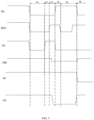
- a display period of the pixel circuit includes an initialization phase, a self-discharge phase, a data preparation phase, a potential control phase, a data writing-in phase, and a light emitting phase that are set successively;
- the driving method includes: in the initialization phase, the self-discharging phase and the data writing-in phase, controlling, by the writing-in control circuit, to connect the first terminal of the first energy storage circuit and the first terminal of the second energy storage circuit under the control of the first writing-in control signal; in the data preparation phase, the potential control phase and the light emitting phase, controlling, by the writing-in control circuit, to disconnect the first terminal of the first energy storage circuit from the first terminal of the second energy storage circuit under the control of the first writing-in control signal.
- the pixel circuit further comprises a first control circuit
- the driving method further comprises: in the initialization phase, the self-discharging phase, the data preparation phase and the light emitting phase, controlling, by the first control circuit, to connect the first terminal of the second energy storage circuit and the second terminal of the second energy storage circuit under the control of the first control signal; in the potential control phase and the data writing-in phase, controlling, by the first control circuit, to connect the first terminal of the second energy storage circuit and the second terminal of the second energy storage circuit under the control of the first control signal.
- an embodiment of the present disclosure provides a driving method applied to the pixel circuit, the driving method comprising: controlling, by the first control circuit, to connect or disconnect the first terminal of the second energy storage circuit and the second terminal of the second energy storage circuit under the control of the first control signal; generating, by the driving circuit, a driving current for driving the light emitting element under the control of the potential of the control terminal of the driving circuit.
- a display period of the pixel circuit includes an initialization phase, a self-discharge phase, a data preparation phase, a potential control phase, a data writing-in phase, and a light emitting phase that are set successively;
- the driving method includes: in the initialization phase, the self-discharging phase, the data preparation phase and the light emitting phase, controlling, by the first control circuit, to connect the first terminal of the second energy storage circuit and the second terminal of the second energy storage circuit under the control of the first control signal; in the potential control phase and the data writing-in phase, controlling, by the first control circuit, to disconnect the first terminal of the second energy storage circuit and the second terminal of the second energy storage circuit under the control of the first control signal.
- the pixel circuit further comprises a writing-in control circuit
- the driving method further comprises: in the initialization phase, the self-discharging phase and the data writing-in phase, controlling, by the writing-in control circuit, to connect the first terminal of the first energy storage circuit and the first terminal of the second energy storage circuit under the control of the first writing-in control signal; in the data preparation phase, the potential control phase and the light emitting phase, controlling, by the writing-in control circuit, to disconnect the first terminal of the first energy storage circuit and the first terminal of the second energy storage circuit under the control of the first writing-in control signal.
- an embodiment of the present disclosure provides a display device comprising the display panel.
- the display panel comprises a first silicon substrate, and a pixel circuit and a gate driving circuit arranged on the first silicon substrate; the display device further includes a second silicon substrate, and a display driver chip arranged on the second silicon substrate.
- an area of the first silicon substrate is larger than an area of the second silicon substrate; a minimum width of signal lines included in the display panel is greater than a width of signal lines included in the display driver chip.
- the transistors used in all embodiments of the present disclosure may be thin film transistors or field effect transistors or other devices with the same characteristics.
- one electrode is called the first electrode, and the other electrode is called the second electrode.
- the first electrode when the transistor is a thin film transistor or a field effect transistor, the first electrode may be a drain electrode, and the second electrode may be a source electrode; or, the first electrode may be a source electrode, the second electrode may be a drain electrode.
- a second terminal of the driving circuit is electrically connected to the light emitting element, and the driving circuit is configured to generate a driving current for driving the light emitting element under the control of a potential of the control terminal of the driving circuit.
- the writing-in control circuit is arranged between the first energy storage circuit and the second energy storage circuit, and the writing-in control circuit controls to connect or disconnect the first terminal of the first energy storage circuit and the first terminal of the second energy storage circuit under the control of the first writing-in control signal; the first energy storage circuit and the second energy storage circuit can control the potential of the control terminal of the driving circuit by dividing the voltage; the driving circuit generates a driving current for driving the light emitting element under the control of the potential of the control terminal of the driving circuit.
- the capacitance value of the first capacitor included in the first energy storage circuit and the capacitance value of the second capacitor included in the second energy storage circuit can be controlled and adjusted, so that the driving current for controlling the driving circuit to drive the light emitting element to emit light is not related to the threshold voltage of the driving transistor included in the driving circuit.
- the embodiments of the present disclosure can provide a current-type pixel circuit with a simple structure and capable of performing threshold voltage self-compensation, which is applied to an Organic Light Emitting Diode (OLED) display.
- OLED Organic Light Emitting Diode
- the second terminal of the driving circuit 11 is electrically connected to the light emitting element E0, and the driving circuit 11 is used to generate a driving current to drive the light emitting element E0 under the control of the potential of the control terminal of the driving circuit.
- the writing-in control circuit 14 controls to connect or disconnect the control terminal of the driving circuit 11 and the first terminal of the second energy storage circuit 13, and the first energy storage circuit 12 and the second energy storage circuit 13 are used to divide the voltage of the data voltage, which expands the dynamic range of the data voltage and is beneficial to the design of the digital-to-analog converter (DAC) in the source driver and the uniformity of the data line output.
- DAC digital-to-analog converter
- the writing-in control circuit 14 controls to disconnect the first terminal of the first energy storage circuit 12 from the first terminal of the second energy storage circuit 13 under the control of the first writing-in control signal.
- the pixel circuit described in at least one embodiment of the present disclosure may further include a first control circuit 15;
- the first control circuit 15 is electrically connected to the first control terminal R0, the first terminal of the second energy storage circuit 13, and the second terminal of the second energy storage circuit 13, is configured to control to connect or disconnect the first terminal of the second energy storage circuit 13 and the second terminal of the second energy storage circuit 13 under the control of the first control signal provided by the first control terminal R0.
- the first control circuit 15 controls to connect the first terminal of the second energy storage circuit 13 and the second terminal of the second energy storage circuit 13 under the control of the first control signal
- the writing-in control circuit 14 controls to disconnect the first terminal of the first energy storage circuit 12 from the first terminal of the second energy storage circuit 13 under the control of the first writing-in control signal
- the driving transistor drives the light emitting element to emit light.
- the pixel circuit described in at least one embodiment of the present disclosure may further include a second control circuit;
- the second control circuit is electrically connected to the second control terminal, the power supply voltage terminal and the first terminal of the driving circuit, and is used to control to connect or disconnect the power supply voltage terminal and the first terminal of the driving circuit under the control of the second control signal provided by the second control terminal.
- the second control circuit can control to connect or disconnect the power supply voltage terminal and the first terminal of the driving circuit under the control of the second control signal, so as to control the self-discharge threshold compensation process of the driving transistor included in the driving circuit.
- the absolute value of the voltage value of the power supply voltage is smaller than the absolute value of the voltage value of the first voltage signal.
- the voltage value range of the power supply voltage may be greater than or equal to 1V and less than or equal to 3V, and the voltage value range of the first voltage signal may be greater than or equal to -8V and less than or equal to -5V, but not limited thereto.
- the second terminal of the driving circuit 11 is electrically connected to the first electrode of the light emitting element E0, and the second electrode of the light emitting element E0 is electrically connected to the first voltage terminal V1.
- the first voltage terminal V1 may be a low voltage terminal, but not limited thereto.
- the pixel circuit further includes a third control circuit; the second terminal of the driving circuit is electrically connected to the first electrode of the light emitting element, and the second electrode of the light emitting element is electrically connected to the first voltage terminal;
- the third control circuit is electrically connected to the third control terminal, the third voltage terminal and the first electrode of the light emitting element, and is used to control to write the third voltage signal provided by the third voltage terminal into the first electrode of the light emitting element under the control of the third control signal provided by the third control terminal.
- the third control circuit is used to write the third voltage signal into the first electrode of the light emitting element during the non-light emitting phase under the control of the third control signal, so that the difference between the potential of the first electrode of the light emitting element and the potential of the second electrode of the light emitting element is smaller than the turn-on voltage of the light emitting element, so as to control the light emitting element not to emit light.
- the third control circuit can reset the potential of the first electrode of the light emitting element, and can also play a shunt function during the light emitting phase to improve the driving accuracy of tiny currents of the silicon-based OLED.
- the light emitting element may be an organic light emitting diode
- the first electrode of the light emitting element is the anode of the organic light emitting diode
- the second electrode of the light emitting element is the cathode of the organic light emitting diode, but not in this way limit.
- the pixel circuit described in at least one embodiment of the present disclosure further includes a third control circuit 20;
- the third control circuit 20 is electrically connected to the third control terminal AZ, the third voltage terminal Vf and the first electrode of the light emitting element E0 respectively, and is configured to control to write the third voltage signal provided by the third voltage terminal Vf into the first electrode of the light emitting element E0 under the control of the second control signal provided by the third control terminal AZ.
- the third control circuit 20 is used to write the third voltage signal provided by the third voltage terminal Vf into the first electrode of the light emitting element E0 under the control of the third control signal during the non-light emitting phase, so that the difference between the potential of the first electrode of the light emitting element E0 and the potential of the second electrode of the light emitting element E0 is smaller than that of the turn-on voltage of light emitting element E0, to control the light emitting element E0 not to emit light.
- the first voltage terminal V1 may be a low voltage terminal, but not limited thereto.
- the writing-in node is electrically connected to the control terminal of the driving circuit, or the writing-in node is electrically connected to the first terminal of the second energy storage circuit.
- the pixel circuit described in at least one embodiment of the present disclosure may further include a reference voltage writing-in circuit 16;
- the reference voltage writing-in circuit is respectively electrically connected to the second writing-in control terminal WS2, the reference voltage terminal R2 and the control terminal of the driving circuit 11, and is configured to write the reference voltage Vref provided by the reference voltage terminal R2 into the control terminal of the driving circuit 11 under the control of the second writing-in control signal provided by the second writing-in control terminal WS2, so as to control the potential of the control terminal of the driving circuit 11.
- the second electrode of the light emitting element is electrically connected to the first voltage terminal.
- the resistor circuit may include a first resistor, but not limited thereto.
- the pixel circuit described in at least one embodiment of the present disclosure may further include a resistor circuit 70;
- the first terminal of the resistor circuit 70 is electrically connected to the second terminal of the driving circuit 11, and the second terminal of the resistor circuit 70 is electrically connected to the first electrode of the light emitting element E0, so as to prevent the short circuit between the first electrode of light emitting element E0 and the second electrode of the light emitting element E0.
- a capacitance value of the second capacitor is smaller than a capacitance value of the first capacitor.
- the capacitance value of the first capacitor needs to be set larger, and the capacitance value of the first capacitor is set to be greater than the capacitance value of the second capacitor.
- a control electrode of the second transistor is electrically connected to the first control terminal, a first electrode of the second transistor is electrically connected to the first terminal of the second energy storage circuit, and a second electrode of the second transistor is electrically connected to the second terminal of the second energy storage circuit; a back gate electrode of the second transistor is electrically connected to the second voltage terminal.
- the reference voltage writing-in circuit includes a third transistor; A control electrode of the third transistor is electrically connected to the second writing-in control terminal, a first electrode of the third transistor is electrically connected to the reference voltage terminal, and a second electrode of the third transistor is electrically connected to the writing-in node; a back gate electrode of the third transistor is electrically connected to the second voltage terminal.
- a control electrode of the driving transistor is the control terminal of the driving circuit, a first electrode of the driving transistor is the first terminal of the driving circuit, and a second electrode of the driving transistor is electrically connected to the second terminal of the driving circuit; a back gate electrode of the driving transistor is electrically connected to the second voltage terminal.
- the third control circuit includes a fifth transistor; A control electrode of the fifth transistor is electrically connected to the third control terminal, a first electrode of the fifth transistor is electrically connected to the third voltage terminal, and a second electrode of the fifth transistor is electrically connected to the first electrode of the light emitting element; a back gate electrode of the fifth transistor is electrically connected to the fourth voltage terminal.
- the driving transistor, the first transistor, the second transistor and the fourth transistor may all be P-type metal-oxide-semiconductor (PMOS) transistors, and the fifth transistor may be N-type metal-oxide-semiconductor (NMOS) transistor, but not limited thereto.
- the driving transistor, the first transistor, the second transistor, the fourth transistor and the fifth transistor may all be PMOS transistors.
- the back gate electrode of each PMOS transistor is electrically connected to the second voltage terminal, but not electrically connected to the power supply voltage terminal, so that the substrate n-hydrazine potential of each PMOS transistor is separated from the power supply voltage, which is facilitate to the bias effect of the base substrate.
- the second voltage terminal may be a high voltage terminal, but not limited thereto.
- a deep n-hydrazine is provided between the back gate electrode of the fifth transistor and the P-type substrate to isolate the back gate electrode of the fifth transistor and the P-type base substrate; the back gate electrode of the fifth transistor and the first electrode of the fifth transistor are both electrically connected to the third voltage terminal.
- the pixel circuit described in at least one embodiment of the present disclosure may further include n-hydrazine; the doping concentration of the n-hydrazine is greater than the doping concentration of the deep n-hydrazine; The ratio of the thickness of the n hydrazine to the thickness of the deep n hydrazine is greater than or equal to 0.4 and less than or equal to 0.6; but not limited thereto.
- the thickness of the n-hydrazine may be 0.5um, and the thickness of the deep-n-hydrazine may be 1um.
- the pixel circuit described in at least one embodiment of the present disclosure may further include p hydrazine; the ratio of the thickness of the p hydrazine to the thickness of the deep n hydrazine is greater than or equal to 0.4 and less than or equal to 0.6; but not limit.
- the thickness of the p hydrazine may be 0.5um, and the thickness of the deep n hydrazine may be 1um.
- the fourth voltage terminal is the third voltage terminal Vf, but not limited thereto.
- the potential of the anode of the organic light emitting diode O1 may be -5V.
- the third voltage signal may be a -5V voltage signal, and the low voltage terminal V0 may provide a -9V voltage signal, but not limited thereto.
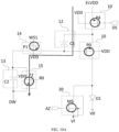
- P0, P1, P2 and P4 are all PMOS transistors, and M5 is an NMOS transistor.
- the second transistor P2 and the second capacitor C2 may be located outside the valid display area, and each column of pixel circuits may share one second transistor and one second capacitor, which is facilitates the realization of a narrow frame; and, in the valid display area, one pixel circuit only includes one capacitor, which can effectively reduce the technology requirements of the circuit.
- Io1 is not related to Vth.
- the power supply voltage may also be raised from ELVDD2 to ELVDD1 first, and then M5 is controlled to be turned off.
- the value range of VDD when the range of ELVDD1 is greater than or equal to 2V and less than or equal to 8V, the value range of VDD can also be greater than or equal to 2V and less than or equal to 8V, and the value range of Vf can be greater than or equal to -6V and less than or equal to 0V; but not limited to this.
- ELUDD1-Vofs may be greater than or equal to 1.5V, but not limited thereto.
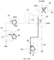
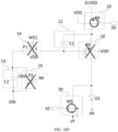
- the transistors corresponding to the circles are turned on, and the transistors corresponding to the crosses are turned off.
- the driving transistor P0 is equivalent to a current source controlled by the gate voltage, so that the data voltage Vdata directly controls the driving current flowing through O1. Therefore, the pixel circuit shown in FIG. 8 of at least one embodiment of the present disclosure adopts a current-type pixel driving method, and the driving transistor included in the driving circuit in at least one embodiment of the pixel circuit shown in FIG.
- the point-strip-line defect when the anode of O1 is short-circuited with the cathode of O1, the point-strip-line defect will occur due to the anode voltage of O1 is negative, when the anode voltage of O1 is negative, the drain voltage of the driving transistor P0 is also a negative voltage, then if the driving transistor is an NMOS transistor, the source voltage of the driving transistor is a negative voltage, and the parasitic diode between the base substrate of the driving transistor and the source electrode of the driving transistor will be turned on in a forward direction, thereby causing a latch effect, resulting in the point-strip-line defect.
- the driving transistor is a PMOS transistor.
- the driving transistor is an NMOS transistor, at least one embodiment of the present disclosure can have a wider anode dynamic range due to the following reasons.
- the driving transistor is an NMOS transistor
- the negative voltage will be connected to the drain electrode of the driving transistor
- the driving transistor is an NMOS transistor
- the driving transistor in the current type pixel circuit is a PMOS transistor
- the potential of the anode of the organic light emitting diode O1 may be a negative voltage.
- At least one embodiment of the pixel circuit shown in FIG. 8 of the present disclosure can perform self-discharge threshold voltage compensation before the data voltage is written, which can improve the display uniformity of the pixel circuit.
- the data voltage is written and divided by two capacitors, which expands the dynamic range of the data voltage and is beneficial to the design of the DAC in the source driver and uniformity of data line output.
- P0 is an NMOS transistor.
- At least one embodiment of the present disclosure sets P0 as a PMOS transistor to solve the above problem.
- At least one embodiment of the pixel circuit shown in FIG. 8 of the present disclosure can prevent the N-type substrate of the first transistor P1 used to transmit the data voltage from leaking current to the drain electrode of the first transistor P1 to the first capacitor C1, while low-grayscale bright spot phenomenon occurs for the following reasons:
- P0 is a PMOS transistor, so in the non-light emitting phase, even if the N-type substrate of the first transistor P1 leaks current to the drain electrode of the first transistor P1 to the first capacitor C1, and the potential of the gate electrode of P0 is increased. Since the driving transistor P0 is also a PMOS transistor, the brightness of the organic light emitting diode O1 will not increase, and no bright spots will appear.
- At least one embodiment of the pixel circuit shown in FIG. 8 of the present disclosure is a current-type pixel circuit, which can compensate for the lifetime attenuation caused by the increase of the internal resistance of the organic light emitting diode O1, and, in the pixel circuit shown in FIG.
- the back gate electrode of each PMOS transistor is connected to the high voltage VDD, but not electrically connected to the power supply voltage terminal, so that the potential of n well of base substrate of each PMOS transistor is separated from the power supply voltage terminal, which is beneficial to bias effect of the base substrate, the potential of the base substrate of the PMOS transistor is higher than the potential of the source electrode of the PMOS transistor, and the back gate effect makes the PMOS transistor to be turned off more completely, which can improve the leakage current Ioff of the switching transistor.
- the fifth transistor M5 is an NMOS transistor, and both the back gate electrode of the fifth transistor M5 and the source electrode of the fifth transistor M5 are electrically connected to the third voltage terminal Vf;
- a deep n hydrazine is provided between the back gate electrode of the fifth transistor M5 and the P-type base substrate to isolate the back gate electrode of the fifth transistor M5 from the P-type base substrate; the back gate electrode of the fifth transistor M5 and the source electrode of the fifth transistor M5 are electrically connected to the third voltage terminal Vf.
- the back gate electrode of the N-type transistor in the pixel circuit and the back gate electrode of the N-type transistor in the driving circuit are both connected to the p type base substrate.
- the back gate electrode of the fifth transistor M5 in the pixel circuit needs to be electrically connected to the third voltage terminal Vf, and the P-type base substrate is connected to a voltage of 0V. Therefore, deep n-hydrazine needs to be set between the P-type base substrate and the back gate electrode of the fifth transistor M5 to isolate the P-type base substrate and the back gate electrode of the fifth transistor M5.
- the dynamic range of the anode of the organic light emitting diode O1 needs to be expanded to negative voltage, the withstand voltage of each transistor is 8V, and ELVDD1 is 3V, the lowest anode reset voltage can be -5V, Therefore, the back gate electrode of the fifth transistor M5 needs to be connected to a -5V voltage signal (generally, the source electrode of the NMOS transistor and the back gate electrode of the NMOS transistor are electrically connected to the same voltage terminal), so it is necessary to isolate the P-type base substrate and the back gate electrode of the fifth transistor M5.
- FIG. 11 is a structural diagram of an NMOS transistor and a PMOS transistor in at least one embodiment of the present disclosure.
- the one labeled 60 is a P-type substrate
- the one labeled 61 is a deep n hydrazine
- the one labeled 621 is a gate electrode of an NMOS transistor
- the one labeled 622 is a gate electrode of a PMOS transistor
- the one labeled 631 is the back gate electrode of the NMOS transistor
- the one labeled 632 is the source electrode of the NMOS transistor
- the one labeled 633 is the drain electrode of the NMOS transistor
- the one labeled 641 is the back gate electrode of the PMOS transistor
- the one labeled 642 is the source electrode of the PMOS transistor
- the one labeled 643 is the drain electrode of the PMOS transistor
- the one labeled 65 is an insulating structure
- the ones labeled 661 and 663 are N hydrazine
- the one labeled 662 is P hydrazine.
- the NMOS transistor may be the fifth transistor.
- a deep n-hydrazine 61 is provided between the back gate electrode 631 of the NMOS transistor and the P-type base substrate 60, so that the back gate electrode of the NMOS transistor can be connected to a -5V voltage signal, and the P-type substrate 60 can be connected to 0V voltage signal.
- FIG. 12 is a schematic structural diagram of an NMOS transistor and a PMOS transistor in the related art.
- FIG. 12 The difference between FIG. 12 and FIG. 11 is that no deep n hydrazine 61 is provided.
- the pixel circuit described in at least one embodiment of the present disclosure further includes a reference voltage writing-in circuit 16;
- the reference voltage writing-in circuit 16 includes a third transistor P3;
- the gate electrode of the third transistor P3 is electrically connected to the second writing-in control terminal WS2, the source electrode of the third transistor P3 is electrically connected to the reference voltage terminal R2, and the drain electrode of the third transistor P3 is electrically connected to the gate electrode of the driving transistor P0; the back gate electrode of the third transistor P3 is electrically connected to the high voltage terminal;
- the reference voltage terminal R2 is used to provide a reference voltage Vref;
- the high voltage terminal is used to provide a high voltage VDD.
- P3 is a PMOS transistor, but not limited thereto.
- the gate electrode of the third transistor P3 is electrically connected to the second writing-in control terminal WS2, the source electrode of the third transistor P3 is electrically connected to the reference voltage terminal R2, and the drain electrode of the third transistor P3 is electrically connected to the first terminal of the second capacitor C2; the back gate electrode of the third transistor P3 is electrically connected to the high voltage terminal; the reference voltage terminal R2 is used to provide a reference voltage Vref; the high voltage terminal is used to provide a high voltage VDD.
- P3 is a PMOS transistor, but not limited thereto.
- the first resistor R01 can prevent a short circuit between the anode of the OLED O1 and the cathode of the OLED O1.
- the first control circuit and the second energy storage circuit are connected in parallel, and the first control circuit is used to control to connect or disconnect the first terminal of the second energy storage circuit the and the second terminal of the second energy storage circuit under the control of the first control signal provided by the first control terminal.
- the second terminal of the driving circuit is electrically connected to the light emitting element, and the driving circuit is used to generate a driving current for driving the light emitting element under the control of the potential of the control terminal of the driving circuit.
- the first control circuit controls to connect or disconnect the first terminal of the second energy storage circuit and the second terminal of the second energy storage circuit under the control of the first control signal; the data voltage is written and divided by the first energy storage circuit and the second energy storage circuit, which expands the dynamic range of the data voltage, which is beneficial to the design of the DAC in the source driver and uniformity of data line output.
- control terminal of the first control circuit is electrically connected to the first control terminal, and the first terminal of the first control circuit is connected to the first terminal of the second energy storage circuit, the second terminal of the first control circuit is electrically connected to the second terminal of the second energy storage circuit.
- the second terminal of the driving circuit 11 is electrically connected to the light emitting element E0, and the driving circuit 11 is used to generate a driving current to drive the light emitting element E0 under the control of the potential of the control terminal of the driving circuit.
- the first control circuit 15 controls to connect or disconnect the first terminal of the second energy storage circuit 13 and the second terminal of the second energy storage circuit 13 under the control of the first control signal; the data voltage is written and divided by the first energy storage circuit 12 and the second energy storage circuit 13, which expands the dynamic range of the data voltage, which is beneficial to the design of the DAC in the source driver and the uniformity of the data line output.
- the first control circuit 15 controls to connect the first terminal of the second energy storage circuit 13 and the second terminal of the second energy storage circuit 13 under the control of the first control signal
- the writing-in control circuit 14 controls to disconnect the first terminal of the first energy storage circuit 12 from the first terminal of the second energy storage circuit 13 under the control of the first writing-in control signal
- the driving transistor drives the light emitting element to emit light.
- the pixel circuit may further include a writing-in control circuit; the writing-in control circuit is arranged between the first energy storage circuit and the second energy storage circuit; A control terminal of the writing-in control circuit is electrically connected to the first writing-in control terminal, a first terminal of the writing-in control circuit is electrically connected to the first terminal of the first energy storage circuit, and a second terminal of the writing-in control circuit is electrically connected to the first terminal of the second energy storage circuit, and the writing-in control circuit is used to control to connect or disconnect the first terminal of the first energy storage circuit and the first terminal of the second energy storage circuit under the control of the first writing-in control signal provided by the first writing-in control terminal.
- the writing-in control circuit is used to control to connect or disconnect the first terminal of the first energy storage circuit and the first terminal of the second energy storage circuit under the control of the first writing-in control signal provided by the first writing-in control terminal.
- the writing-in control circuit controls to connect the first terminal of the first energy storage circuit and the first terminal of the second energy storage circuit under the control of the first writing-in control signal;
- the writing-in control circuit controls to disconnect the first terminal of the first energy storage circuit and the first terminal of the second energy storage circuit under the control of the first writing-in control signal.
- the pixel circuit described in at least one embodiment of the present disclosure further includes a second control circuit;
- the second control circuit is electrically connected to the second control terminal, the power supply voltage terminal and the first terminal of the driving circuit, and is used to control to connect or disconnect the power supply voltage terminal and the first terminal of the driving circuit under the control of the second control signal provided by the second control terminal.
- the second control circuit can control to connect or disconnect the power supply voltage terminal and the first terminal of the driving circuit under the control of the second control signal, so as to control the self-discharge threshold compensation process of the driving transistor included in the driving circuit.
- the absolute value of the voltage value of the power supply voltage is smaller than the absolute value of the voltage value of the first voltage signal.
- the voltage value range of the power supply voltage may be greater than or equal to 1V and less than or equal to 3V, and the voltage value range of the first voltage signal may be greater than or equal to -8V and less than or equal to -5V, but is not the limit.
- the pixel circuit described in at least one embodiment of the present disclosure may further include a third control circuit; the second terminal of the driving circuit is electrically connected to the first electrode of the light emitting element, and the second electrode of the light emitting element is electrically connected to the first voltage terminal;
- the third control circuit is electrically connected to the third control terminal, the third voltage terminal and the first electrode of the light emitting element, and is used to control to write the third voltage signal provided by the third voltage terminal into the first electrode of the light emitting element.
- the third control circuit is used to write the third voltage signal provided by the third voltage terminal into the first electrode of the light emitting element in the non-light emitting phase under the control of the third control signal, so that the difference between the potential of the first electrode of the light emitting element and the potential of the second electrode of the light emitting element is smaller than the turn-on voltage of the light emitting element, so as to control the light emitting element not to emit light.
- the third control circuit can reset the potential of the first electrode of the light emitting element, and can also play a shunt function during the light emitting phase to improve the driving accuracy of tiny current of the high silicon-based OLED.
- the writing-in node is electrically connected to the control terminal of the driving circuit, or the writing-in node is electrically connected to the first terminal of the second energy storage circuit.
- the pixel circuit may further include a resistor circuit; A first terminal of the resistor circuit is electrically connected to the second terminal of the driving circuit, and a second terminal of the resistor circuit is electrically connected to the first electrode of the light emitting element, so as to prevent the short circuit between the first electrode of the light emitting element and the second electrode of the light emitting element.
- the second electrode of the light emitting element is electrically connected to the first voltage terminal.
- the capacitance value of the second capacitor is smaller than the capacitance value of the first capacitor.
- the capacitance value of the first capacitor needs to be set larger, and the capacitance value of the first capacitor is set to be greater than the capacitance value of the second capacitor.
- the writing-in control circuit includes a first transistor; A control electrode of the first transistor is electrically connected to the first writing-in control terminal, a first electrode of the first transistor is electrically connected to the control terminal of the driving circuit, and a second electrode of the first transistor is electrically connected to the first terminal of the second energy storage circuit; a back gate electrode of the first transistor is electrically connected to the second voltage terminal.
- the first control circuit includes a second transistor; A control electrode of the second transistor is electrically connected to the first control terminal, a first electrode of the second transistor is electrically connected to the first terminal of the second energy storage circuit, and a second electrode of the second transistor is electrically connected to the second terminal of the second energy storage circuit; a back gate electrode of the second transistor is electrically connected to the second voltage terminal.
- the reference voltage writing-in circuit includes a third transistor; A control electrode of the third transistor is electrically connected to the second writing-in control terminal, a first electrode of the third transistor is electrically connected to the reference voltage terminal, and a second electrode of the third transistor is electrically connected to the writing-in node; a back gate electrode of the third transistor is electrically connected to the second voltage terminal.
- a control terminal of the driving transistor is the control terminal of the driving circuit, a first electrode of the driving transistor is the first terminal of the driving circuit, and a second electrode of the driving transistor is the second terminal of the driving circuit; a back gate electrode of the driving transistor is electrically connected to the second voltage terminal.
- the third control circuit includes a fifth transistor; A control electrode of the fifth transistor is electrically connected to the third control terminal, a first electrode of the fifth transistor is electrically connected to the third voltage terminal, and a second electrode of the fifth transistor is electrically connected to the first electrode of the light emitting terminal; a back gate electrode of the fifth transistor is electrically connected with the fourth voltage terminal.
- the fifth transistor may be an n-type transistor; the fourth voltage terminal is a third voltage terminal; A deep n hydrazine is arranged between the back gate electrode of the fifth transistor and the P-type base substrate to isolate the back gate electrode of the fifth transistor from the P-type base substrate; the back gate electrode of the fifth transistor and the first electrode of the fifth transistor are both electrically connected to the reset voltage terminal.
- the pixel circuit described in at least one embodiment of the present disclosure may further include n-hydrazine; the doping concentration of the n-hydrazine is greater than the doping concentration of the deep n-hydrazine; The ratio of the thickness of the n hydrazine to the thickness of the deep n hydrazine is greater than or equal to 0.4 and less than or equal to 0.6; but not limited thereto.
- the thickness of the n-hydrazine may be 0.5um, and the thickness of the deep-n-hydrazine may be 1um.
- the pixel circuit described in at least one embodiment of the present disclosure may further include p hydrazine; the ratio of the thickness of the p hydrazine to the thickness of the deep n hydrazine is greater than or equal to 0.4 and less than or equal to 0.6; but not limit.
- the thickness of the p hydrazine may be 0.5um, and the thickness of the deep n hydrazine may be 1um.
- the cathode of the OLED O1 is connected to the common electrode voltage Vcom.
- the fourth voltage terminal is the high voltage terminal
- the first voltage terminal is connected to the common electrode voltage Vcom
- the third voltage terminal is the ground terminal G1.
- ELVDD-Vref is greater than or equal to 1.5V, and the value range of ELVDD may be greater than or equal to 2V and less than or equal to 8V, but it is not limited thereto.
- all transistors are PMOS transistors, but not limited thereto.
- the driving transistor P0 is equivalent to a current source controlled by the gate voltage, so as to realize direct control of the driving current flowing through O1 by the data voltage Vdata, so the pixel circuit shown in FIG. 17 of at least one embodiment of the present disclosure is a current-type pixel circuit.
- the data voltage Vdata is divided by C1 and C2 and written into the gate electrode of the driving transistor P0, so as to expand the dynamic range of the data voltage Vdata, which is beneficial to the design of the DAC in the source driver and the uniformity of the data line output.
- the gate-source voltage of the driving transistor P0 can compensate the threshold voltage of the driving transistor, so that the light emitting current of the organic light emitting diode O1 is not related to the threshold voltage Vth, thereby improving display uniformity.
- At least one embodiment of the pixel circuit shown in FIG. 17 of the present disclosure is a current-type pixel circuit using all PMOS transistors, which has a wider anode dynamic range than a current-type pixel circuit including NMOS transistors under the same process platform. The reasons are as follows.
- the current-mode pixel circuit using a PMOS transistor has a wider anode dynamic range, when the transistors in the current-mode pixel circuit are all PMOS transistors, the potential of the anode of the organic light emitting diode O1 may be a negative voltage.
- At least one embodiment of the pixel circuit shown in FIG. 17 of the present disclosure adopts a current-type pixel driving method
- the driving transistor included in the driving circuit in at least one embodiment of the pixel circuit shown in FIG. 17 of the present disclosure is a PMOS transistor, when the anode of O1 and the cathode of O1 are short-circuited, the dot-strip-line defect will not occur because the anode voltage of O1 is negative.
- At least one embodiment of the pixel circuit shown in FIG. 17 of the present disclosure can prevent the N-type base substrate of the first transistor P1 used to transmit the data voltage from leaking to the drain electrode of the first transistor P1 to the first capacitor C1, thus the low-grayscale bright spot phenomenon occurs for the following reasons.
- the transistor used in at least one embodiment of the pixel circuit shown in FIG. 17 in the present disclosure is a PMOS transistor. Therefore, in the non-light emitting phase, even if the N-type base substrate of the first transistor P1 leaks current to the drain electrode of the first transistor P1 to the first capacitor C1 to increase the potential of the gate electrode of P0, since the driving transistor P0 is also a PMOS transistor, it will not increase the brightness of the organic light emitting diode, and no bright spots will occur.
- P0 is an NMOS transistor
- at least one embodiment of the present disclosure sets the transistor as a PMOS transistor to solve the above problem.
- At least one embodiment of the pixel circuit shown in FIG. 17 of the present disclosure is a current-type pixel circuit, which can compensate for the lifetime attenuation caused by the increase of the internal resistance of the organic light emitting diode O1, and in the pixel circuit shown in FIG. 17 of the present disclosure, the back gate electrode of each transistor is connected to the high voltage VDD, but not connected to ELVDD, so that the potential of base substrate nwell potential of each transistor is separated from ELVDD, so that ELVDD can be flexibly set in a range less than VDD.
- At least one embodiment of the pixel circuit shown in FIG. 17 of the present disclosure may be a current-type pixel circuit applied to a silicon-based OLED micro-display chip, but not limited thereto. At least one embodiment of the present disclosure is based on a specific semiconductor process platform. Only PMOS transistors are used for pixel circuit design, which overcomes the space of MOS transistors limited by the design rule in the pixel circuit where PMOS transistors and NMOS transistors coexist. It can effectively decrease the pixel area and increase Pixels Per Inch (PPI, the number of pixels per inch).
- PPI Pixels Per Inch
- the display panel described in the embodiments of the present disclosure includes a plurality of rows and a plurality of columns of the pixel circuits.
- the second capacitor may be a parasitic capacitance between the data line and the signal line arranged on the same layer as the second capacitor, so as to save layout space.
- the display panel includes a valid display area and a peripheral area, and the peripheral area surrounds the valid display area;
- the pixel circuit includes a first control circuit;
- the first control circuit and the second energy storage circuit are arranged in the peripheral area, and the components included in the pixel circuit other than the first control circuit and the second energy storage circuit are arranged in the valid display area.
- the first control circuit and the second energy storage circuit may be located in the peripheral area, and each column of pixel circuits may share one first control circuit and one second energy storage circuit, so as to realize a narrow frame; and in the valid display area, one pixel circuit only includes one capacitor, which can effectively reduce the process requirements of the circuit.
- a column of pixel circuits shares one second transistor P2 and one second capacitor C2.
- the driving method described in at least one embodiment of the present disclosure is applied to the above-mentioned pixel circuit, and the driving method includes:
- the display period of the pixel circuit includes an initialization phase, a self-discharge phase, a data preparation phase, a potential control phase, a data writing-in phase, and a light emitting phase that are set successively;
- the driving method includes:
- the pixel circuit further includes a first control circuit; the driving method further includes:
- the driving method described in at least one embodiment of the present disclosure is applied to the above-mentioned pixel circuit, and the driving method includes:
- the display period of the pixel circuit includes an initialization phase, a self-discharge phase, a data preparation phase, a potential control phase, a data writing-in phase, and a light emitting phase that are set successively;
- the driving method includes:
- the pixel circuit further includes a writing-in control circuit; the driving method further includes:
- the display device described in the embodiment of the present disclosure includes the above-mentioned display panel.
- the display panel includes a first silicon substrate, and a pixel circuit and a gate driving circuit arranged on the first silicon substrate;
- the display device further includes a second silicon substrate, and a display driver chip arranged on the second silicon substrate.
- the display device further includes a second silicon substrate 203 and a display driver chip arranged on the second silicon substrate 203.
- the display driver chip may include a display driver integrated circuit 301, a source driver 302, a timing controller 303, a data processor 304, an input and output interface 305, a signal receiver 306, and a bias and reference voltage supply circuit 307; but not limited thereto.
- the area of the first silicon substrate is larger than the area of the second silicon substrate;
- the minimum width of the signal lines included in the display panel is greater than the width of the signal lines included in the display driver chip.
- the display panel can be manufactured by using a 100nm process
- the display driver chip can be manufactured by a 28nm process.
- the distance between the signal lines included in the display driver chip is smaller than the distance between the signal lines included in the display panel.
- the display device may be any product or component with a display function, such as a mobile phone, a tablet computer, a television, a monitor, a notebook computer, a digital photo frame, a navigator, and the like.
Landscapes
- Engineering & Computer Science (AREA)
- Physics & Mathematics (AREA)
- Computer Hardware Design (AREA)
- General Physics & Mathematics (AREA)
- Theoretical Computer Science (AREA)
- Control Of Indicators Other Than Cathode Ray Tubes (AREA)
- Electroluminescent Light Sources (AREA)
- Control Of El Displays (AREA)
Applications Claiming Priority (1)
| Application Number | Priority Date | Filing Date | Title |
|---|---|---|---|
| PCT/CN2022/096196 WO2023230826A1 (zh) | 2022-05-31 | 2022-05-31 | 像素电路、显示面板、驱动方法和显示装置 |
Publications (2)
| Publication Number | Publication Date |
|---|---|
| EP4421790A1 true EP4421790A1 (de) | 2024-08-28 |
| EP4421790A4 EP4421790A4 (de) | 2025-04-02 |
Family
ID=89026568
Family Applications (1)
| Application Number | Title | Priority Date | Filing Date |
|---|---|---|---|
| EP22944165.4A Pending EP4421790A4 (de) | 2022-05-31 | 2022-05-31 | Pixelschaltung, anzeigetafel, ansteuerungsverfahren und anzeigevorrichtung |
Country Status (6)
| Country | Link |
|---|---|
| US (2) | US12307967B2 (de) |
| EP (1) | EP4421790A4 (de) |
| JP (1) | JP2025517266A (de) |
| KR (1) | KR20250018458A (de) |
| CN (1) | CN117501342A (de) |
| WO (1) | WO2023230826A1 (de) |
Families Citing this family (3)
| Publication number | Priority date | Publication date | Assignee | Title |
|---|---|---|---|---|
| KR20250007101A (ko) * | 2023-07-04 | 2025-01-14 | 삼성디스플레이 주식회사 | 드라이버 및 이를 포함하는 표시 장치 |
| CN119832846A (zh) * | 2023-10-12 | 2025-04-15 | 合肥维信诺科技有限公司 | 像素电路及显示模组 |
| KR20260007375A (ko) * | 2024-07-03 | 2026-01-14 | 삼성디스플레이 주식회사 | 화소 및 이를 포함하는 표시 장치 |
Family Cites Families (23)
| Publication number | Priority date | Publication date | Assignee | Title |
|---|---|---|---|---|
| JP2006300980A (ja) | 2005-04-15 | 2006-11-02 | Seiko Epson Corp | 電子回路、その駆動方法、電気光学装置、及び電子機器 |
| JP2006317696A (ja) | 2005-05-12 | 2006-11-24 | Sony Corp | 画素回路および表示装置、並びに画素回路の制御方法 |
| CN101536070B (zh) | 2007-01-31 | 2012-01-18 | 夏普株式会社 | 像素电路及显示装置 |
| JP2012255872A (ja) * | 2011-06-08 | 2012-12-27 | Sony Corp | 画素回路、表示装置、電子機器、及び、画素回路の駆動方法 |
| JP6099336B2 (ja) | 2011-09-14 | 2017-03-22 | 株式会社半導体エネルギー研究所 | 発光装置 |
| TW201316315A (zh) * | 2011-10-05 | 2013-04-16 | Wintek Corp | 發光元件驅動電路及其相關的畫素電路與應用 |
| JP6141590B2 (ja) | 2011-10-18 | 2017-06-07 | セイコーエプソン株式会社 | 電気光学装置および電子機器 |
| JP5821685B2 (ja) | 2012-02-22 | 2015-11-24 | セイコーエプソン株式会社 | 電気光学装置および電子機器 |
| US9335598B2 (en) * | 2012-05-30 | 2016-05-10 | Sharp Kabushiki Kaisha | Display device and method for driving same |
| TW201426709A (zh) | 2012-12-26 | 2014-07-01 | Sony Corp | 顯示裝置、顯示裝置之驅動方法及電子機器 |
| JP6131662B2 (ja) * | 2013-03-22 | 2017-05-24 | セイコーエプソン株式会社 | 表示装置及び電子機器 |
| JP2015138252A (ja) * | 2014-01-24 | 2015-07-30 | ソニー株式会社 | 表示装置および電子機器 |
| CN104821150B (zh) | 2015-04-24 | 2018-01-16 | 北京大学深圳研究生院 | 像素电路及其驱动方法和显示装置 |
| CN110634902B (zh) * | 2016-06-13 | 2021-08-17 | 深圳大学 | 一种超高速快门半导体影像传感器 |
| CN108932929B (zh) * | 2017-05-23 | 2020-06-30 | 上海视欧光电科技有限公司 | Oled像素电路及图像显示装置 |
| TWI837280B (zh) * | 2019-03-29 | 2024-04-01 | 日商索尼半導體解決方案公司 | 光檢測裝置及電子機器 |
| CN110349540A (zh) * | 2019-07-26 | 2019-10-18 | 京东方科技集团股份有限公司 | 像素驱动电路、显示装置及像素驱动电路的控制方法 |
| CN111968585B (zh) * | 2020-08-27 | 2021-12-07 | 京东方科技集团股份有限公司 | 像素电路、像素驱动方法和显示装置 |
| CN112071269A (zh) * | 2020-09-24 | 2020-12-11 | 京东方科技集团股份有限公司 | 像素单元驱动电路、驱动方法、显示面板及显示装置 |
| CN112053661B (zh) | 2020-09-28 | 2023-04-11 | 京东方科技集团股份有限公司 | 像素电路、像素驱动方法、显示面板和显示装置 |
| CN113053297A (zh) * | 2021-03-15 | 2021-06-29 | 京东方科技集团股份有限公司 | 像素电路、像素驱动方法和显示装置 |
| US12190820B2 (en) | 2021-04-26 | 2025-01-07 | Chengdu Boe Optoelectronics Technology Co., Ltd. | Pixel circuit, pixel driving method and display device |
| US11935470B2 (en) | 2021-04-30 | 2024-03-19 | Chengdu Boe Optoelectronics Technology Co., Ltd. | Pixel circuit and driving method thereof, and display device |
-
2022
- 2022-05-31 JP JP2024543496A patent/JP2025517266A/ja active Pending
- 2022-05-31 WO PCT/CN2022/096196 patent/WO2023230826A1/zh not_active Ceased
- 2022-05-31 KR KR1020247024729A patent/KR20250018458A/ko active Pending
- 2022-05-31 CN CN202280001576.2A patent/CN117501342A/zh active Pending
- 2022-05-31 US US18/262,699 patent/US12307967B2/en active Active
- 2022-05-31 EP EP22944165.4A patent/EP4421790A4/de active Pending
-
2025
- 2025-05-02 US US19/197,640 patent/US20250265999A1/en active Pending
Also Published As
| Publication number | Publication date |
|---|---|
| US12307967B2 (en) | 2025-05-20 |
| US20250265999A1 (en) | 2025-08-21 |
| US20240395199A1 (en) | 2024-11-28 |
| EP4421790A4 (de) | 2025-04-02 |
| CN117501342A (zh) | 2024-02-02 |
| KR20250018458A (ko) | 2025-02-06 |
| JP2025517266A (ja) | 2025-06-05 |
| WO2023230826A1 (zh) | 2023-12-07 |
Similar Documents
| Publication | Publication Date | Title |
|---|---|---|
| US20250166567A1 (en) | Pixel circuit, driving method and display device | |
| US11393396B2 (en) | Pixel circuit and driving method therefor and display panel | |
| US11798473B2 (en) | Pixel driving circuit and display panel | |
| US11830427B2 (en) | Pixel circuit, display apparatus and driving method | |
| US20240144880A1 (en) | Pixel driving circuit and driving method thereof, display substrate and display device | |
| US12142218B2 (en) | Pixel circuit, display panel, and display apparatus | |
| US11749199B1 (en) | Pixel driving circuit and display device | |
| US20250265999A1 (en) | Pixel circuit, display panel, driving method and display device | |
| US20200126478A1 (en) | Pixel circuit and driving method thereof, display device | |
| US11763730B2 (en) | Pixel driving circuit having an initialization and compensation and display panel | |
| US20160035276A1 (en) | Oled pixel circuit, driving method of the same, and display device | |
| CN111429836A (zh) | 一种像素驱动电路和显示面板 | |
| US12236865B2 (en) | Method of driving display device, including charge maintenance stage | |
| US20210027706A1 (en) | Pixel compensation circuit, driving method, electroluminescent display panel and display device | |
| CN111599308A (zh) | 显示装置及其控制方法、电子设备 | |
| US20250273153A1 (en) | Pixel circuit, display panel, driving method and display device | |
| US10553159B2 (en) | Pixel circuit, display panel and display device | |
| US12322339B2 (en) | Display panel | |
| US11195454B2 (en) | Pixel driving circuit, driving method thereof, display panel and display device | |
| CN110400536B (zh) | 一种像素电路及其驱动方法、显示面板 | |
| US12230214B2 (en) | Array substrate, display panel and driving method of array substrate | |
| CN113539171A (zh) | 显示像素电路、显示像素电路驱动方法及显示面板 | |
| US20250246136A1 (en) | Pixel circuit, driving method thereof, and display device |
Legal Events
| Date | Code | Title | Description |
|---|---|---|---|
| STAA | Information on the status of an ep patent application or granted ep patent |
Free format text: STATUS: THE INTERNATIONAL PUBLICATION HAS BEEN MADE |
|
| PUAI | Public reference made under article 153(3) epc to a published international application that has entered the european phase |
Free format text: ORIGINAL CODE: 0009012 |
|
| STAA | Information on the status of an ep patent application or granted ep patent |
Free format text: STATUS: REQUEST FOR EXAMINATION WAS MADE |
|
| 17P | Request for examination filed |
Effective date: 20240521 |
|
| AK | Designated contracting states |
Kind code of ref document: A1 Designated state(s): AL AT BE BG CH CY CZ DE DK EE ES FI FR GB GR HR HU IE IS IT LI LT LU LV MC MK MT NL NO PL PT RO RS SE SI SK SM TR |
|
| A4 | Supplementary search report drawn up and despatched |
Effective date: 20250227 |
|
| RIC1 | Information provided on ipc code assigned before grant |
Ipc: G09G 3/3233 20160101ALI20250221BHEP Ipc: G09G 3/3208 20160101AFI20250221BHEP |
|
| DAV | Request for validation of the european patent (deleted) | ||
| DAX | Request for extension of the european patent (deleted) |