EP4418539A1 - Pipelined successive-approximation analog-to-digital converter, integrated circuit, and electronic device - Google Patents
Pipelined successive-approximation analog-to-digital converter, integrated circuit, and electronic device Download PDFInfo
- Publication number
- EP4418539A1 EP4418539A1 EP22896989.5A EP22896989A EP4418539A1 EP 4418539 A1 EP4418539 A1 EP 4418539A1 EP 22896989 A EP22896989 A EP 22896989A EP 4418539 A1 EP4418539 A1 EP 4418539A1
- Authority
- EP
- European Patent Office
- Prior art keywords
- capacitor
- analog
- digital
- bit
- capacitors
- Prior art date
- Legal status (The legal status is an assumption and is not a legal conclusion. Google has not performed a legal analysis and makes no representation as to the accuracy of the status listed.)
- Pending
Links
Images
Classifications
-
- H—ELECTRICITY
- H03—ELECTRONIC CIRCUITRY
- H03M—CODING; DECODING; CODE CONVERSION IN GENERAL
- H03M1/00—Analogue/digital conversion; Digital/analogue conversion
- H03M1/12—Analogue/digital converters
- H03M1/20—Increasing resolution using an n bit system to obtain n + m bits
-
- H—ELECTRICITY
- H03—ELECTRONIC CIRCUITRY
- H03M—CODING; DECODING; CODE CONVERSION IN GENERAL
- H03M1/00—Analogue/digital conversion; Digital/analogue conversion
- H03M1/12—Analogue/digital converters
- H03M1/34—Analogue value compared with reference values
- H03M1/38—Analogue value compared with reference values sequentially only, e.g. successive approximation type
- H03M1/46—Analogue value compared with reference values sequentially only, e.g. successive approximation type with digital/analogue converter for supplying reference values to converter
- H03M1/466—Analogue value compared with reference values sequentially only, e.g. successive approximation type with digital/analogue converter for supplying reference values to converter using switched capacitors
- H03M1/468—Analogue value compared with reference values sequentially only, e.g. successive approximation type with digital/analogue converter for supplying reference values to converter using switched capacitors in which the input S/H circuit is merged with the feedback DAC array
-
- H—ELECTRICITY
- H03—ELECTRONIC CIRCUITRY
- H03M—CODING; DECODING; CODE CONVERSION IN GENERAL
- H03M1/00—Analogue/digital conversion; Digital/analogue conversion
- H03M1/12—Analogue/digital converters
- H03M1/34—Analogue value compared with reference values
- H03M1/38—Analogue value compared with reference values sequentially only, e.g. successive approximation type
- H03M1/46—Analogue value compared with reference values sequentially only, e.g. successive approximation type with digital/analogue converter for supplying reference values to converter
- H03M1/462—Details of the control circuitry, e.g. of the successive approximation register
-
- H—ELECTRICITY
- H03—ELECTRONIC CIRCUITRY
- H03M—CODING; DECODING; CODE CONVERSION IN GENERAL
- H03M1/00—Analogue/digital conversion; Digital/analogue conversion
- H03M1/12—Analogue/digital converters
- H03M1/1205—Multiplexed conversion systems
-
- H—ELECTRICITY
- H03—ELECTRONIC CIRCUITRY
- H03M—CODING; DECODING; CODE CONVERSION IN GENERAL
- H03M1/00—Analogue/digital conversion; Digital/analogue conversion
- H03M1/12—Analogue/digital converters
- H03M1/14—Conversion in steps with each step involving the same or a different conversion means and delivering more than one bit
- H03M1/16—Conversion in steps with each step involving the same or a different conversion means and delivering more than one bit with scale factor modification, i.e. by changing the amplification between the steps
- H03M1/164—Conversion in steps with each step involving the same or a different conversion means and delivering more than one bit with scale factor modification, i.e. by changing the amplification between the steps the steps being performed sequentially in series-connected stages
-
- H—ELECTRICITY
- H03—ELECTRONIC CIRCUITRY
- H03M—CODING; DECODING; CODE CONVERSION IN GENERAL
- H03M1/00—Analogue/digital conversion; Digital/analogue conversion
- H03M1/12—Analogue/digital converters
-
- H—ELECTRICITY
- H03—ELECTRONIC CIRCUITRY
- H03M—CODING; DECODING; CODE CONVERSION IN GENERAL
- H03M1/00—Analogue/digital conversion; Digital/analogue conversion
- H03M1/12—Analogue/digital converters
- H03M1/34—Analogue value compared with reference values
-
- H—ELECTRICITY
- H03—ELECTRONIC CIRCUITRY
- H03M—CODING; DECODING; CODE CONVERSION IN GENERAL
- H03M1/00—Analogue/digital conversion; Digital/analogue conversion
- H03M1/12—Analogue/digital converters
- H03M1/34—Analogue value compared with reference values
- H03M1/38—Analogue value compared with reference values sequentially only, e.g. successive approximation type
-
- Y—GENERAL TAGGING OF NEW TECHNOLOGICAL DEVELOPMENTS; GENERAL TAGGING OF CROSS-SECTIONAL TECHNOLOGIES SPANNING OVER SEVERAL SECTIONS OF THE IPC; TECHNICAL SUBJECTS COVERED BY FORMER USPC CROSS-REFERENCE ART COLLECTIONS [XRACs] AND DIGESTS
- Y02—TECHNOLOGIES OR APPLICATIONS FOR MITIGATION OR ADAPTATION AGAINST CLIMATE CHANGE
- Y02D—CLIMATE CHANGE MITIGATION TECHNOLOGIES IN INFORMATION AND COMMUNICATION TECHNOLOGIES [ICT], I.E. INFORMATION AND COMMUNICATION TECHNOLOGIES AIMING AT THE REDUCTION OF THEIR OWN ENERGY USE
- Y02D10/00—Energy efficient computing, e.g. low power processors, power management or thermal management
Definitions
- the disclosure relates to a field of integrated circuit technology, and in particular, to a pipelined successive approximation register analog-to-digital converter, an integrated circuit, and an electronic device.
- the pipelined successive approximation register analog-to-digital converter has been widely used in various ADC scenarios due to a relatively high speed and high accuracy.
- the pipelined SAR ADC generally includes at least two stages of SAR ADCs, each having a digital-to-analog converter (DAC), a comparator, and an SAR logic unit, and a residue amplifier is provided between the DACs of two adjacent stages of SAR ADCs, to amplify a sampling residual signal of a previous stage of SAR ADC and then transmit the amplified signal to a next stage of SAR ADC.
- DAC digital-to-analog converter
- the existing art proposes to reduce a reference voltage in the next stage of ADC to half of a reference voltage in the previous stage of ADC, so as to implement inter-stage gain halving of the two-stage structure, and reduce a gain of the residue amplifier.
- the halved reference voltage may greatly reduce the conversion speed and the power consumption of the ADC.
- An embodiment of the present disclosure provides a pipelined successive approximation register analog-to-digital converter, an integrated circuit, and an electronic device.
- an embodiment of the present disclosure provides a pipelined successive approximation register analog-to-digital converter, including: a first-stage successive approximation register analog-to-digital converter, including a first digital-to-analog converter, a first comparator and a first digital control logic unit sequentially connected, wherein the first digital-to-analog converter includes a first capacitor array having one first complement bit capacitor and M bit first capacitors, a first end of the first complement bit capacitor and a first end of each of the first capacitors are respectively connected to an analog input voltage, a second end of each of the first capacitors is connected to a positive going reference voltage or a negative going reference voltage through a multi-way selection switch, and a second end of the first complement bit capacitor is connected to a negative going reference voltage; a capacitance value of the first complement bit capacitor is equal to a capacitance value of a first bit capacitor in the M bit first capacitors, and capacitance values of the M bit first capacitors are sequentially increased by a
- an embodiment of the present disclosure provides an integrated circuit, including a pipelined successive approximation register analog-to-digital converter as described in the first aspect.
- an embodiment of the present disclosure provides an electronic device, including an integrated circuit as described in the second aspect.
- phrases "at least one of" and similar expressions refer to any group of the listed items, including any combination of one or more of the listed items.
- at least one of a, b or c may represent: a, b, c, a and b, a and c, b and c, or a and b and c, where a, b and c may be in single or multiple forms.
- a pipelined successive approximation register analog-to-digital converter generally includes multiple stages of SAR ADCs and is configured to encode digital signals output from the multiple stages of SAR ADCs and output final digital signals converted from analog input signals.
- Each stage of SAR ADC mainly includes three parts: a digital-to-analog converter (DAC), a comparator, and an SAR logic unit.
- the basic working principle of each stage of SAR ADC is as follows: in the first period after sampling, the most significant bit (MSB) of the DAC is set to 1, while other bits are set to 0, and initial values (typically half of a full-scale voltage) of the analog input voltage and the DAC output voltage is compared by the comparator.
- MSB most significant bit
- a current bit is coded to 1, while an on/off state of the DAC remains unchanged; and if the analog input voltage is less than the DAC output voltage, the current bit is coded to 0, while the on/off state of the DAC returns to a state before the action. Then, the SAR logic moves to a next bit, where the on/off state of the DAC is changed again, and a comparison with the analog input voltage is performed, so on and so forth, until a last bit is compared and all A/D conversion codes are obtained.
- a core idea of the SAR ADC working principle is a bisection method, where the DAC output voltage is changed by 1/2 each time and successively approximate the analog input voltage, thereby implementing analog-to-digital conversion.
- a residue amplifier is provided between the DACs of two adjacent stages of SAR ADCs, and configured to amplify a residue (residual voltage) of the analog input voltage of a previous stage of SAR ADC to be used as an analog input for a next stage of SAR ADC.
- the existing art proposes to reduce a reference voltage in the next stage of SAR ADC to half of a reference voltage in the previous stage of SAR ADC, so as to implement inter-stage gain halving of the two-stage structure, and reduce a gain of the residue amplifier.
- an amplification factor of the residue amplifier should be set to at least 2 M-1 , and through the inter-stage gain halving technique, the amplification factor of the residue amplifier can be reduced to 2 M-2 .
- halving the inter-stage gain by halving the reference voltage will greatly reduce the conversion speed and the power consumption of the ADC.
- the conventional pipelined successive approximation register analog-to-digital converter of two or more stages has the defect of a high gain of the residue amplifier, and thus is not suitable for a deep submicron CMOS process.
- the method of halving the reference voltage in the existing art although can halve the inter-stage gain, will restrict the overall speed and precision of the pipelined successive approximation register analog-to-digital converter, and thus increase the power consumption.
- an embodiment of the present disclosure provides a pipelined successive approximation register analog-to-digital converter, an integrated circuit, and an electronic device which can be used to halve the inter-stage gain without halving the reference voltage, thereby increasing the conversion speed and reducing the power consumption of the ADC.
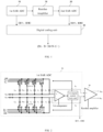
- FIG. 1 is a block diagram of a pipelined successive approximation register analog-to-digital converter according to an embodiment of the present disclosure.
- the pipelined successive approximation register analog-to-digital converter according to the embodiment of the present disclosure includes: a first-stage successive approximation register analog-to-digital converter 10, a residue amplifier 30, a second-stage successive approximation register analog-to-digital converter 20, and a digital coding unit 40.
- the first-stage successive approximation register analog-to-digital converter 10 is connected to the second-stage successive approximation register analog-to-digital converter 20 through the residue amplifier 30, and the first-stage successive approximation register analog-to-digital converter 10 and the second-stage successive approximation register analog-to-digital converter 20 are respectively connected to the digital coding unit 40.
- the first-stage successive approximation register analog-to-digital converter 10 in the embodiment of the present disclosure is configured as an M bit SAR ADC, that is, the first SAR ADC is configured to output M bit digital signals to the digital coding unit 40, where M is an integer greater than 1.
- the second-stage successive approximation register analog-to-digital converter 20 in the embodiment of the present disclosure is configured as an N bit SAR ADC, that is, the second SAR ADC is configured to output N bit digital signals to the digital coding unit 40, where N is an integer greater than 1.
- the digital coding unit 40 encodes the M bit digital signals (B11:B1M) output from the first SAR ADC and the N bit digital signals (B21:B2N) output from the second SAR ADC by an inter-stage dislocation accumulation method, to obtain the final (M+N-1) bit binary digital signals (D1: D (M+N-1)).
- the first SAR ADC includes a first digital-to-analog converter, a first comparator and a first digital control logic unit sequentially connected.
- the first digital-to-analog converter includes a first capacitor array having one first complement bit capacitor C 0 and M bit first capacitors C 1 to C M .
- Capacitance values of the M bit first capacitors C 1 to C M are sequentially increased by a power of 2 from small to large according to the number of bits.
- a first end of the first complement bit capacitor C 0 and a first end of each of the first capacitors C 1 to C M are respectively connected to an analog input voltage; a second end of each of the first capacitors C 1 to C M is connected to a positive going reference voltage V ref or a negative going reference voltage through a multi-way selection switch (in this example, a reference ground GND is used as the negative going reference voltage), and a second end of the first complement bit capacitor C 0 is constantly connected to a negative going reference voltage.
- the analog input voltage may be connected to an input end of the first digital to analog converter by a sample and hold circuit (S/H).
- S/H sample and hold circuit
- A/D conversion of an analog signal takes some time, within which the analog signal has to remain substantially unchanged to ensure the conversion precision.
- the sample and hold circuit is a circuit for this purpose.
- the first SAR ADC samples the analog input voltage by an upper plate.
- the upper plate of each capacitor is connected to the analog input voltage
- lower plates of the M bit first capacitors C 1 to C M are connected to multiple reference signal sources through a multi-way selection switch.
- each reference signal source may include a positive going reference voltage V ref and a negative going reference voltage (in this example, the reference ground GND is used as the negative going reference voltage).
- the reference signal source further includes a common mode voltage V CM .
- a lower plate of the first complement bit capacitor C 0 is constantly connected to a negative going reference voltage.
- the first SAR ADC adopts a differential upper plate sampling mode, and analog input voltages input to the first SAR ADC are differential voltages V ip1 and V in1 , where V ip1 is a positive going analog input voltage, and V in1 is a negative going analog input voltage.
- V ip1 is a positive going analog input voltage
- V in1 is a negative going analog input voltage.
- the upper plate differential sampling mode two first capacitor arrays with the same structure are provided in the first SAR ADC, and the two first capacitor arrays are correspondingly connected to a positive going analog input voltage and a negative going analog input voltage.
- each first capacitor array includes M+1 capacitors, resulting in 2 M+2 capacitors in total in the first SAR ADC.
- C 1 to C M-1 are weight capacitors, and in the successive approximation conversion process, an output voltage of the first capacitor array can be increased/decreased by switching on/off the corresponding weight capacitors; and the C M is configured to generate a residual voltage signal to the second SAR ADC.
- circuitry of the first SAR ADC shown in FIG. 2 is merely exemplary, and in specific implementations, the circuitry of the first SAR ADC can be adaptively varied depending on the analog sampling mode. For example, when a single-ended sampling mode is adopted, the first SAR ADC is provided with only one first capacitor array.
- the residue amplifier 30 is positioned between the first SAR ADC and the second SAR ADC. Specifically, an input end of the residue amplifier 30 is connected to a residual voltage output from the first digital-to-analog converter.
- the residue amplifier 30 employs a differential amplifier.
- the residue amplifier 30 has two input end correspondingly connected to residual voltages (a positive going residual voltage and a negative going residual voltage) output from two first capacitor arrays.
- the residue amplifier 30 amplifies the residual voltage of V ip1 and V in1 to obtain differential analog input voltages V ip2 and V in2 . Accordingly, the residue amplifier 30 has two output ends to output V ip2 and V in2 to the second SAR ADC.
- the two input ends of the residue amplifier 30 may be further provided with respective switches (S1, S2), through which input of the residual voltage is controlled.
- FIG. 3 shows a schematic circuitry diagram of a second SAR ADC according to an embodiment of the present disclosure.
- the second SAR ADC includes a second digital-to-analog converter, a second comparator and a second digital control logic unit sequentially connected.
- the second digital-to-analog converter includes a second capacitor array having one gain halving capacitor C a , one second complement bit capacitor C 0 , and N-1 bit second capacitors C 1 to C N-1 .
- Capacitance values of the N-1 bit second capacitors C 1 to C N-1 are sequentially increased by a power of 2 from small to large according to the number of bits.
- a first end of the gain halving capacitor C a , a first end of the second complement bit capacitor C 0 , and a first end of each of the N-1 bit second capacitors C 1 to C N-1 are respectively connected to an output end of the residue amplifier 30.
- Second ends of the N-1 bit second capacitors C 1 to C N-1 are respectively connected to a positive going reference voltage V ref and a negative going reference voltage (in this example, a reference ground GND is used as the negative going reference voltage) through a multi-way selection switch, and second ends of the gain halving capacitor C a and the second position-complementing capacitor C 0 are both constantly connected to a negative going reference voltage.
- the second SAR ADC samples the analog input voltage by an upper plate.
- an upper plate of each capacitor is connected to the output end of the residue amplifier 30, to access an analog input voltage (obtained by amplifying a residual voltage of the first SAR ADC by the residue amplifier 30) from the residue amplifier 30, while lower plates of the N-1 bit second capacitors C 1 to C N-1 are connected to multiple reference signal sources through a multi-way selection switch.
- each reference signal source may include a positive going reference voltage V ref and a negative going reference voltage (in this example, the reference ground GND is used as the negative going reference voltage).
- the reference signal source further includes a common mode voltage V CM .
- Lower plates of the gain halving capacitor C a and the second position-complementing capacitor C 0 are both constantly connected to a negative going reference voltage.
- the second SAR ADC adopts a differential upper plate sampling mode, and two output ends of the residue amplifier 30 output differential voltages V ip2 and V in2 (obtained by amplifying a residual voltage of V ip1 and V in1 of the first SAR ADC by the residue amplifier 30), where V ip2 is a positive going analog input voltage, and V in2 is a negative going analog input voltage.
- each first capacitor array includes N+1 capacitors (one gain halving capacitor, one second complement bit capacitor, and N-1 bit second capacitors), resulting in 2N+2 capacitors in total in the second SAR ADC.
- C 1 to C N-1 are all weight capacitors, and in the successive approximation conversion process, an output voltage of the second capacitor array can be increased/decreased by switching on/off the corresponding weight capacitors.
- circuitry of the second SAR ADC shown in FIG. 3 is merely exemplary, and in specific implementations, the circuitry of the second SAR ADC can be adaptively varied depending on the analog sampling mode. For example, when a single-ended sampling mode is adopted, the second SAR ADC is provided with only one second capacitor array.
- the digital coding unit 40 is connected to output ends of the first digital control logic unit and the second digital control logic unit. After amplification and quantization by the two-stage successive approximation register analog-to-digital converter and the residue amplifier 30, the analog input voltage generates (M+N) bit codes, and finally, the resulting (M+N-1) bit digital codes are output through the digital coding unit 40.
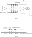
- FIG. 4 shows a schematic encoding process by the digital coding unit 40.
- the first SAR ADC M-bit SAR ADC
- the second SAR ADC N-bit SAR ADC
- the resulting (M+N-1) bit binary digital output codes D1:D (M+N-1)
- a decoding circuit may implement the encoding process of FIG. 4 by means of a full adder (FA) and a half adder (HA).
- FA full adder
- HA half adder
- a gain halving capacitor is provided in a second digital-to-analog converter in the second-stage successive approximation register analog-to-digital converter 20, and a capacitance value of the gain halving capacitor is a sum of capacitance values of the rest capacitors in the second digital-to-analog converter, so that a capacitance DAC of the second-stage successive approximation register analog-to-digital converter 20 is doubled, inter-stage gain halving of the two-stage structure is implemented, and a gain of the residue amplifier 30 is reduced (the amplification factor of the residue amplifier 30 is reduced from 2 M-1 to 2 M-2 ), while a positive going reference voltage of the second-stage successive approximation register analog-to-digital converter 20 is not halved and remains consistent with the positive going reference voltage of the first-stage successive approximation register analog-to-digital converter 10, which can effectively reduce the power consumption while increasing the conversion speed, and can be adapted to
- the analog input signal After amplification and quantization by the two-stage successive approximation register analog-to-digital converter and the inter-stage amplifier, the analog input signal generates (M+N) bit digit signals, and finally, the (M+N-1) bit digit signals are output through the digital coding unit 40.
- An embodiment of the present disclosure further provides an integrated circuit, including a pipelined successive approximation register analog-to-digital converter according to any one of the above embodiments.
- an embodiment of the present disclosure further provides an electronic device, including a device body, and an integrated circuit as described above, where the integrated circuit is provided in the device body.
- the electronic device may be a network device (e.g., a base station device) or the like.
- a gain halving capacitor is provided in a second digital-to-analog converter in the second-stage successive approximation register analog-to-digital converter, and a capacitance value of the gain halving capacitor is a sum of capacitance values of the rest capacitors in the second digital-to-analog converter, which can implement inter-stage gain halving of the two-stage structure, and reduce a gain of the residue amplifier, while a positive going reference voltage of the second-stage successive approximation register analog-to-digital converter is not halved and remains consistent with the positive going reference voltage of the first-stage successive approximation register analog-to-digital converter, which can effectively reduce the power consumption while increasing the conversion speed, and can be adapted to a deep submicron CMOS process .
- the analog input signal After amplification and quantization by the two-stage successive approximation register analog-to-digital converter and the inter-stage amplifier, the analog input signal generates (M+N) bit digit signals, and finally, the (M+N-1) bit digit signals are output through the digital coding unit.
Landscapes
- Engineering & Computer Science (AREA)
- Theoretical Computer Science (AREA)
- Power Engineering (AREA)
- Analogue/Digital Conversion (AREA)
Abstract
Description
- The present application is based on and claims priority from the
Chinese patent application No. 202111407728.2 filed on November 24, 2021 - The disclosure relates to a field of integrated circuit technology, and in particular, to a pipelined successive approximation register analog-to-digital converter, an integrated circuit, and an electronic device.
- The pipelined successive approximation register analog-to-digital converter (pipelined SAR ADC) has been widely used in various ADC scenarios due to a relatively high speed and high accuracy. The pipelined SAR ADC generally includes at least two stages of SAR ADCs, each having a digital-to-analog converter (DAC), a comparator, and an SAR logic unit, and a residue amplifier is provided between the DACs of two adjacent stages of SAR ADCs, to amplify a sampling residual signal of a previous stage of SAR ADC and then transmit the amplified signal to a next stage of SAR ADC. In a deep submicron CMOS process, the intrinsic gain of the transistor is gradually reduced, making it difficult to implement high-gain linear amplification by the residue amplifier. In view of this technical problem, the existing art proposes to reduce a reference voltage in the next stage of ADC to half of a reference voltage in the previous stage of ADC, so as to implement inter-stage gain halving of the two-stage structure, and reduce a gain of the residue amplifier. However, the halved reference voltage may greatly reduce the conversion speed and the power consumption of the ADC.
- An embodiment of the present disclosure provides a pipelined successive approximation register analog-to-digital converter, an integrated circuit, and an electronic device.
- In a first aspect, an embodiment of the present disclosure provides a pipelined successive approximation register analog-to-digital converter, including: a first-stage successive approximation register analog-to-digital converter, including a first digital-to-analog converter, a first comparator and a first digital control logic unit sequentially connected, wherein the first digital-to-analog converter includes a first capacitor array having one first complement bit capacitor and M bit first capacitors, a first end of the first complement bit capacitor and a first end of each of the first capacitors are respectively connected to an analog input voltage, a second end of each of the first capacitors is connected to a positive going reference voltage or a negative going reference voltage through a multi-way selection switch, and a second end of the first complement bit capacitor is connected to a negative going reference voltage; a capacitance value of the first complement bit capacitor is equal to a capacitance value of a first bit capacitor in the M bit first capacitors, and capacitance values of the M bit first capacitors are sequentially increased by a power of 2 from small to large according to the number of bits, where M is an integer larger than 1; a residue amplifier having an input end connected to a residual voltage output from the first digital-to-analog converter; a second-stage successive approximation register analog-to-digital converter, including a second digital-to-analog converter, a second comparator and a second digital control logic unit sequentially connected, wherein the second digital-to-analog converter includes a second capacitor array having one gain halving capacitor, one second complement bit capacitor, and N-1 bit second capacitors, a first end of the gain halving capacitor, a first end of the second complement bit capacitor, and a first end of each of the second capacitors are respectively connected to an output end of the residue amplifier, a second end of each of the second capacitors is connected to a positive going reference voltage or a negative going reference voltage through a multi-way selection switch, and a second end of the gain halving capacitor, and a second end of the second complement bit capacitor are respectively connected to a negative going reference voltage, a capacitance value of the second complement bit capacitor is equal to a capacitance value of a first bit capacitor in the N-1 bit second capacitors, capacitance values of the N-1 bit second capacitors are sequentially increased by a power of 2 from small to large according to the number of bits, and a capacitance value of the gain halving capacitor is a sum of the capacitance values of the N-1 bit second capacitors and the second complement bit capacitor, where N is an integer greater than 1; and a digital coding unit connected to output ends of the first digital control logic unit and the second digital control logic unit.
- In a second aspect, an embodiment of the present disclosure provides an integrated circuit, including a pipelined successive approximation register analog-to-digital converter as described in the first aspect.
- In a third aspect, an embodiment of the present disclosure provides an electronic device, including an integrated circuit as described in the second aspect.
-
-
FIG. 1 is a block diagram of a pipelined successive approximation register analog-to-digital converter according to an embodiment of the present disclosure; -
FIG. 2 is a schematic circuitry diagram of a first-stage successive approximation register analog-to-digital converter according to an embodiment of the present disclosure; -
FIG. 3 is a schematic circuitry diagram of a second-stage successive approximation register analog-to-digital converter according to an embodiment of the present disclosure; and -
FIG. 4 is a schematic diagram showing an encoding process by a digital coding unit according to an embodiment of the present disclosure. - The technical solutions in the embodiments of the present disclosure will be described below with reference to the drawings in the embodiments of the present disclosure, and it is obvious that the described embodiments are only some, but not all, embodiments of the present disclosure. All other embodiments obtained by a person of ordinary skill in the art based on the embodiments in the present disclosure without any creative labor belong to the protection scope of the present disclosure.
- It will be appreciated that in the description of the embodiments of the present disclosure, should there be any reference to "first", "second" or the like, it is merely intended to distinguish technical features, instead of being interpreted as indicating or implying any relative importance or implying any number of the indicated technical features or implying any precedence of the indicated technical features. The phrase "at least one" means one or more, and "a plurality" means two or more. The term "and/or" describes an association relationship of associated objects, which may include three relationships; for example, A and/or B may refer to: A alone, A and B, or B alone, where A and B may be in singular or plural forms. The character "/" generally indicates that the former and latter associated objects are in an "or" relationship. The phrase "at least one of" and similar expressions refer to any group of the listed items, including any combination of one or more of the listed items. For example, at least one of a, b or c may represent: a, b, c, a and b, a and c, b and c, or a and b and c, where a, b and c may be in single or multiple forms.
- To facilitate understanding of the technical solutions in the embodiments of the present disclosure, a brief description of the pipelined successive approximation register analog-to-digital converter in the existing art is firstly given below.
- A pipelined successive approximation register analog-to-digital converter generally includes multiple stages of SAR ADCs and is configured to encode digital signals output from the multiple stages of SAR ADCs and output final digital signals converted from analog input signals.
- Each stage of SAR ADC mainly includes three parts: a digital-to-analog converter (DAC), a comparator, and an SAR logic unit. The basic working principle of each stage of SAR ADC is as follows: in the first period after sampling, the most significant bit (MSB) of the DAC is set to 1, while other bits are set to 0, and initial values (typically half of a full-scale voltage) of the analog input voltage and the DAC output voltage is compared by the comparator. If the analog input voltage is greater than the DAC output voltage, a current bit is coded to 1, while an on/off state of the DAC remains unchanged; and if the analog input voltage is less than the DAC output voltage, the current bit is coded to 0, while the on/off state of the DAC returns to a state before the action. Then, the SAR logic moves to a next bit, where the on/off state of the DAC is changed again, and a comparison with the analog input voltage is performed, so on and so forth, until a last bit is compared and all A/D conversion codes are obtained. A core idea of the SAR ADC working principle is a bisection method, where the DAC output voltage is changed by 1/2 each time and successively approximate the analog input voltage, thereby implementing analog-to-digital conversion.
- For the pipelined successive approximation register analog-to-digital converter, a residue amplifier is provided between the DACs of two adjacent stages of SAR ADCs, and configured to amplify a residue (residual voltage) of the analog input voltage of a previous stage of SAR ADC to be used as an analog input for a next stage of SAR ADC.
- In a deep submicron CMOS process, the intrinsic gain of the transistor is gradually reduced, making it difficult to implement high-gain linear amplification by the residue amplifier. In view of this technical problem, the existing art proposes to reduce a reference voltage in the next stage of SAR ADC to half of a reference voltage in the previous stage of SAR ADC, so as to implement inter-stage gain halving of the two-stage structure, and reduce a gain of the residue amplifier. For example, if the previous stage of SAR ADC has M bits, an amplification factor of the residue amplifier should be set to at least 2M-1, and through the inter-stage gain halving technique, the amplification factor of the residue amplifier can be reduced to 2M-2. However, halving the inter-stage gain by halving the reference voltage will greatly reduce the conversion speed and the power consumption of the ADC.
- In summary, the conventional pipelined successive approximation register analog-to-digital converter of two or more stages has the defect of a high gain of the residue amplifier, and thus is not suitable for a deep submicron CMOS process. The method of halving the reference voltage in the existing art, although can halve the inter-stage gain, will restrict the overall speed and precision of the pipelined successive approximation register analog-to-digital converter, and thus increase the power consumption. In view of this, an embodiment of the present disclosure provides a pipelined successive approximation register analog-to-digital converter, an integrated circuit, and an electronic device which can be used to halve the inter-stage gain without halving the reference voltage, thereby increasing the conversion speed and reducing the power consumption of the ADC.
- Referring to
FIG. 1, FIG. 1 is a block diagram of a pipelined successive approximation register analog-to-digital converter according to an embodiment of the present disclosure. As shown inFIG. 1 , the pipelined successive approximation register analog-to-digital converter according to the embodiment of the present disclosure includes: a first-stage successive approximation register analog-to-digital converter 10, aresidue amplifier 30, a second-stage successive approximation register analog-to-digital converter 20, and adigital coding unit 40. The first-stage successive approximation register analog-to-digital converter 10 is connected to the second-stage successive approximation register analog-to-digital converter 20 through theresidue amplifier 30, and the first-stage successive approximation register analog-to-digital converter 10 and the second-stage successive approximation register analog-to-digital converter 20 are respectively connected to thedigital coding unit 40. - It will be understood that the first-stage successive approximation register analog-to-digital converter 10 (hereinafter "the first SAR ADC") in the embodiment of the present disclosure is configured as an M bit SAR ADC, that is, the first SAR ADC is configured to output M bit digital signals to the
digital coding unit 40, where M is an integer greater than 1. the second-stage successive approximation register analog-to-digital converter 20 (hereinafter "the second SAR ADC") in the embodiment of the present disclosure is configured as an N bit SAR ADC, that is, the second SAR ADC is configured to output N bit digital signals to thedigital coding unit 40, where N is an integer greater than 1. Thedigital coding unit 40 encodes the M bit digital signals (B11:B1M) output from the first SAR ADC and the N bit digital signals (B21:B2N) output from the second SAR ADC by an inter-stage dislocation accumulation method, to obtain the final (M+N-1) bit binary digital signals (D1: D (M+N-1)). - Referring to
FIG. 2 , a schematic circuitry diagram of a first SAR ADC according to an embodiment of the present disclosure is shown. The first SAR ADC includes a first digital-to-analog converter, a first comparator and a first digital control logic unit sequentially connected. The first digital-to-analog converter includes a first capacitor array having one first complement bit capacitor C0 and M bit first capacitors C1 to CM. - Capacitance values of the M bit first capacitors C1 to CM are sequentially increased by a power of 2 from small to large according to the number of bits. The capacitance value of a first capacitance Ci may be expressed by: Ci=2i-1*CU, where i = an integer selected from any one of 1 to M, and CU is a unit capacitance.
- A capacitance value of the first complement bit capacitor C0 is equal to a capacitance value of a first bit capacitor C1 in the M bit first capacitors, i.e., C0= CU.
- As shown in
FIG. 2 , a first end of the first complement bit capacitor C0 and a first end of each of the first capacitors C1 to CM are respectively connected to an analog input voltage; a second end of each of the first capacitors C1 to CM is connected to a positive going reference voltage Vref or a negative going reference voltage through a multi-way selection switch (in this example, a reference ground GND is used as the negative going reference voltage), and a second end of the first complement bit capacitor C0 is constantly connected to a negative going reference voltage. - It will be understood that the analog input voltage may be connected to an input end of the first digital to analog converter by a sample and hold circuit (S/H). A/D conversion of an analog signal takes some time, within which the analog signal has to remain substantially unchanged to ensure the conversion precision. The sample and hold circuit is a circuit for this purpose.
- As shown in
FIG. 2 , the first SAR ADC samples the analog input voltage by an upper plate. In the first SAR ADC, the upper plate of each capacitor is connected to the analog input voltage, while lower plates of the M bit first capacitors C1 to CM are connected to multiple reference signal sources through a multi-way selection switch. Exemplarily, each reference signal source may include a positive going reference voltage Vref and a negative going reference voltage (in this example, the reference ground GND is used as the negative going reference voltage). In some examples, the reference signal source further includes a common mode voltage VCM. A lower plate of the first complement bit capacitor C0 is constantly connected to a negative going reference voltage. - In the example shown in
FIG. 2 , the first SAR ADC adopts a differential upper plate sampling mode, and analog input voltages input to the first SAR ADC are differential voltages Vip1 and Vin1, where Vip1 is a positive going analog input voltage, and Vin1 is a negative going analog input voltage. In the upper plate differential sampling mode, two first capacitor arrays with the same structure are provided in the first SAR ADC, and the two first capacitor arrays are correspondingly connected to a positive going analog input voltage and a negative going analog input voltage. For the first SAR ADC with an M-bit differential output, each first capacitor array includes M+1 capacitors, resulting in 2M+2 capacitors in total in the first SAR ADC. - It will be understood that among the M bit first capacitors in the first capacitor array, C1 to CM-1 are weight capacitors, and in the successive approximation conversion process, an output voltage of the first capacitor array can be increased/decreased by switching on/off the corresponding weight capacitors; and the CM is configured to generate a residual voltage signal to the second SAR ADC.
- It will be understood that the circuitry of the first SAR ADC shown in
FIG. 2 is merely exemplary, and in specific implementations, the circuitry of the first SAR ADC can be adaptively varied depending on the analog sampling mode. For example, when a single-ended sampling mode is adopted, the first SAR ADC is provided with only one first capacitor array. - In the embodiments of the present disclosure, the
residue amplifier 30 is positioned between the first SAR ADC and the second SAR ADC. Specifically, an input end of theresidue amplifier 30 is connected to a residual voltage output from the first digital-to-analog converter. - As shown in
FIG. 2 , in the case that the first SAR ADC adopts a differential upper plate sampling mode, theresidue amplifier 30 employs a differential amplifier. In the case of using a differential amplifier, theresidue amplifier 30 has two input end correspondingly connected to residual voltages (a positive going residual voltage and a negative going residual voltage) output from two first capacitor arrays. Theresidue amplifier 30 amplifies the residual voltage of Vip1 and Vin1 to obtain differential analog input voltages Vip2 and Vin2. Accordingly, theresidue amplifier 30 has two output ends to output Vip2 and Vin2 to the second SAR ADC. - It will be understood that the two input ends of the
residue amplifier 30 may be further provided with respective switches (S1, S2), through which input of the residual voltage is controlled. - Referring to
FIG. 3, FIG. 3 shows a schematic circuitry diagram of a second SAR ADC according to an embodiment of the present disclosure. As shown inFIG. 3 , the second SAR ADC includes a second digital-to-analog converter, a second comparator and a second digital control logic unit sequentially connected. The second digital-to-analog converter includes a second capacitor array having one gain halving capacitor Ca, one second complement bit capacitor C0, and N-1 bit second capacitors C1 to CN-1. - Capacitance values of the N-1 bit second capacitors C1 to CN-1 are sequentially increased by a power of 2 from small to large according to the number of bits. The capacitance value of a second capacitance Ci may be expressed by: Ci=2i-1*CU, where i = an integer selected from any one of 1 to N-1, and CU is a unit capacitance.
- A capacitance value of the second complement bit capacitor C0 is equal to a capacitance value of a first bit capacitor C1 in the N-1 bit second capacitors C1 to CN-1, i.e., C0= CU.
- A capacitance value of the gain halving capacitor Ca is a sum of the capacitance values of the N-1 bit second capacitors C1 to CN-1 and the second complement bit capacitor C0, where the capacitance value of Ca may be expressed by: Ca= 2N-1*CU.
- As shown in
FIG. 3 , a first end of the gain halving capacitor Ca, a first end of the second complement bit capacitor C0, and a first end of each of the N-1 bit second capacitors C1 to CN-1 are respectively connected to an output end of theresidue amplifier 30. Second ends of the N-1 bit second capacitors C1 to CN-1 are respectively connected to a positive going reference voltage Vref and a negative going reference voltage (in this example, a reference ground GND is used as the negative going reference voltage) through a multi-way selection switch, and second ends of the gain halving capacitor Ca and the second position-complementing capacitor C0 are both constantly connected to a negative going reference voltage. - As shown in
FIG. 3 , the second SAR ADC samples the analog input voltage by an upper plate. In the second SAR ADC, an upper plate of each capacitor is connected to the output end of theresidue amplifier 30, to access an analog input voltage (obtained by amplifying a residual voltage of the first SAR ADC by the residue amplifier 30) from theresidue amplifier 30, while lower plates of the N-1 bit second capacitors C1 to CN-1are connected to multiple reference signal sources through a multi-way selection switch. Exemplarily, each reference signal source may include a positive going reference voltage Vref and a negative going reference voltage (in this example, the reference ground GND is used as the negative going reference voltage). In some examples, the reference signal source further includes a common mode voltage VCM. Lower plates of the gain halving capacitor Ca and the second position-complementing capacitor C0 are both constantly connected to a negative going reference voltage. - In the example shown in
FIG. 3 , the second SAR ADC adopts a differential upper plate sampling mode, and two output ends of theresidue amplifier 30 output differential voltages Vip2 and Vin2 (obtained by amplifying a residual voltage of Vip1 and Vin1 of the first SAR ADC by the residue amplifier 30), where Vip2 is a positive going analog input voltage, and Vin2 is a negative going analog input voltage. - In the upper plate differential sampling mode, two second capacitor arrays with the same structure are provided in the second SAR ADC, and the two second capacitor arrays are correspondingly connected to the positive going analog input voltage Vip2 and the negative going analog input voltage Vin2. For the second SAR ADC with an N-bit differential output, each first capacitor array includes N+1 capacitors (one gain halving capacitor, one second complement bit capacitor, and N-1 bit second capacitors), resulting in 2N+2 capacitors in total in the second SAR ADC.
- It will be understood that among the N-1 second capacitors in the second capacitor array, C1 to CN-1 are all weight capacitors, and in the successive approximation conversion process, an output voltage of the second capacitor array can be increased/decreased by switching on/off the corresponding weight capacitors.
- It will be understood that the circuitry of the second SAR ADC shown in
FIG. 3 is merely exemplary, and in specific implementations, the circuitry of the second SAR ADC can be adaptively varied depending on the analog sampling mode. For example, when a single-ended sampling mode is adopted, the second SAR ADC is provided with only one second capacitor array. - In the embodiments of the present disclosure, the
digital coding unit 40 is connected to output ends of the first digital control logic unit and the second digital control logic unit. After amplification and quantization by the two-stage successive approximation register analog-to-digital converter and theresidue amplifier 30, the analog input voltage generates (M+N) bit codes, and finally, the resulting (M+N-1) bit digital codes are output through thedigital coding unit 40. -
FIG. 4 shows a schematic encoding process by thedigital coding unit 40. The first SAR ADC (M-bit SAR ADC) and the second SAR ADC (N-bit SAR ADC) jointly generate (M+N) bit codes, and finally, the resulting (M+N-1) bit binary digital output codes (D1:D (M+N-1)) are obtained based on the inter-stage dislocation accumulation mode ofFIG. 3 . To maintain full swing quantization, a subtraction process of entry digital codes is performed. A decoding circuit may implement the encoding process ofFIG. 4 by means of a full adder (FA) and a half adder (HA). - According to the solution provided in the embodiments of the present disclosure, a gain halving capacitor is provided in a second digital-to-analog converter in the second-stage successive approximation register analog-to-
digital converter 20, and a capacitance value of the gain halving capacitor is a sum of capacitance values of the rest capacitors in the second digital-to-analog converter, so that a capacitance DAC of the second-stage successive approximation register analog-to-digital converter 20 is doubled, inter-stage gain halving of the two-stage structure is implemented, and a gain of theresidue amplifier 30 is reduced (the amplification factor of theresidue amplifier 30 is reduced from 2M-1 to 2M-2), while a positive going reference voltage of the second-stage successive approximation register analog-to-digital converter 20 is not halved and remains consistent with the positive going reference voltage of the first-stage successive approximation register analog-to-digital converter 10, which can effectively reduce the power consumption while increasing the conversion speed, and can be adapted to a deep submicron CMOS process . After amplification and quantization by the two-stage successive approximation register analog-to-digital converter and the inter-stage amplifier, the analog input signal generates (M+N) bit digit signals, and finally, the (M+N-1) bit digit signals are output through thedigital coding unit 40. - It should be noted that the solution provided in the embodiments of the present disclosure is not limited to be applied to a two-stage successive approximation register analog-to-digital converter, but also a successive approximation register analog-to-digital converter of three or more stages.
- An embodiment of the present disclosure further provides an integrated circuit, including a pipelined successive approximation register analog-to-digital converter according to any one of the above embodiments.
- In addition, an embodiment of the present disclosure further provides an electronic device, including a device body, and an integrated circuit as described above, where the integrated circuit is provided in the device body. Exemplarily, the electronic device may be a network device (e.g., a base station device) or the like.
- According to the solution provided in the embodiments of the present disclosure, a gain halving capacitor is provided in a second digital-to-analog converter in the second-stage successive approximation register analog-to-digital converter, and a capacitance value of the gain halving capacitor is a sum of capacitance values of the rest capacitors in the second digital-to-analog converter, which can implement inter-stage gain halving of the two-stage structure, and reduce a gain of the residue amplifier, while a positive going reference voltage of the second-stage successive approximation register analog-to-digital converter is not halved and remains consistent with the positive going reference voltage of the first-stage successive approximation register analog-to-digital converter, which can effectively reduce the power consumption while increasing the conversion speed, and can be adapted to a deep submicron CMOS process . After amplification and quantization by the two-stage successive approximation register analog-to-digital converter and the inter-stage amplifier, the analog input signal generates (M+N) bit digit signals, and finally, the (M+N-1) bit digit signals are output through the digital coding unit.
- While the present disclosure has been described with reference to several implementations above, the present disclosure is not limited to the above implementations, and various equivalent variations or replacements may be made by those skilled in the art without departing from the spirit of the present disclosure. Such equivalent variations or replacements fall into the scope as defined in the claims of the present disclosure.
Claims (10)
- A pipelined successive approximation register analog-to-digital converter, comprising:a first-stage successive approximation register analog-to-digital converter, including a first digital-to-analog converter, a first comparator and a first digital control logic unit sequentially connected, wherein the first digital-to-analog converter includes a first capacitor array having one first complement bit capacitor and M bit first capacitors, a first end of the first complement bit capacitor and a first end of each of the first capacitors are respectively connected to an analog input voltage, a second end of each of the first capacitors is connected to a positive going reference voltage or a negative going reference voltage through a multi-way selection switch, and a second end of the first complement bit capacitor is connected to a negative going reference voltage; a capacitance value of the first complement bit capacitor is equal to a capacitance value of a first bit capacitor in the M bit first capacitors, and capacitance values of the M bit first capacitors are sequentially increased by a power of 2 from small to large according to the number of bits, where M is an integer larger than 1;a residue amplifier having an input end connected to a residual voltage output from the first digital-to-analog converter;a second-stage successive approximation register analog-to-digital converter, including a second digital-to-analog converter, a second comparator and a second digital control logic unit sequentially connected, wherein the second digital-to-analog converter includes a second capacitor array having one gain halving capacitor, one second complement bit capacitor, and N-1 bit second capacitors, a first end of the gain halving capacitor, a first end of the second complement bit capacitor, and a first end of each of the second capacitors are respectively connected to an output end of the residue amplifier, a second end of each of the second capacitors is connected to a positive going reference voltage or a negative going reference voltage through a multi-way selection switch, and a second end of the gain halving capacitor, and a second end of the second complement bit capacitor are respectively connected to a negative going reference voltage, a capacitance value of the second complement bit capacitor is equal to a capacitance value of a first bit capacitor in the N-1 bit second capacitors, capacitance values of the N-1 bit second capacitors are sequentially increased by a power of 2 from small to large according to the number of bits, and a capacitance value of the gain halving capacitor is a sum of the capacitance values of the N-1 bit second capacitors and the second complement bit capacitor, where N is an integer greater than 1; anda digital coding unit connected to output ends of the first digital control logic unit and the second digital control logic unit.
- The pipelined successive approximation register analog-to-digital converter according to claim 1, wherein the analog input voltage is a differential voltage; and two first capacitor arrays are provided and correspondingly connected to a positive going input voltage and a negative going input voltage in the differential voltage.
- The pipelined successive approximation register analog-to-digital converter according to claim 2, wherein the residue amplifier is a differential amplifier having two input ends correspondingly connected to residual voltages output from the two first capacitor arrays.
- The pipelined successive approximation register analog-to-digital converter according to claim 3, wherein the differential amplifier has two output ends; and two second capacitor arrays are provided and correspondingly connected to the two output ends of the differential amplifier.
- The pipelined successive approximation register analog-to-digital converter according to claim 1, wherein the residue amplifier has an amplification factor being an (M-2)th power of 2.
- The pipelined successive approximation register analog-to-digital converter according to claim 1, wherein the second end of each first capacitor is further connected to a common mode voltage through the multi-way selection switch.
- The pipelined successive approximation register analog-to-digital converter according to claim 1, wherein the second end of each second capacitor is further connected to a common mode voltage through the multi-way selection switch.
- The pipelined successive approximation register analog-to-digital converter according to claim 1, further comprising a sample and hold circuit connected to the analog input voltage and the first digital-to-analog converter.
- An integrated circuit, comprising a pipelined successive approximation register analog-to-digital converter according to any one of claims 1 to 8.
- An electronic device, comprising a device body, and an integrated circuit according to claim 9, wherein the integrated circuit is provided in the device body.
Applications Claiming Priority (2)
| Application Number | Priority Date | Filing Date | Title |
|---|---|---|---|
| CN202111407728.2A CN116170021B (en) | 2021-11-24 | 2021-11-24 | Pipeline successive approximation analog-to-digital converter, integrated circuit and electronic device |
| PCT/CN2022/078889 WO2023092887A1 (en) | 2021-11-24 | 2022-03-02 | Pipelined successive-approximation analog-to-digital converter, integrated circuit, and electronic device |
Publications (2)
| Publication Number | Publication Date |
|---|---|
| EP4418539A1 true EP4418539A1 (en) | 2024-08-21 |
| EP4418539A4 EP4418539A4 (en) | 2025-10-29 |
Family
ID=86420575
Family Applications (1)
| Application Number | Title | Priority Date | Filing Date |
|---|---|---|---|
| EP22896989.5A Pending EP4418539A4 (en) | 2021-11-24 | 2022-03-02 | Pipeline analog-to-digital converter with step-by-step approach, integrated circuit and electronic device |
Country Status (5)
| Country | Link |
|---|---|
| US (1) | US12512848B2 (en) |
| EP (1) | EP4418539A4 (en) |
| JP (2) | JP7794968B2 (en) |
| CN (1) | CN116170021B (en) |
| WO (1) | WO2023092887A1 (en) |
Families Citing this family (7)
| Publication number | Priority date | Publication date | Assignee | Title |
|---|---|---|---|---|
| CN113746481B (en) * | 2021-09-13 | 2024-04-02 | 澳门大学 | Pipelined successive approximation analog-to-digital converter |
| CN117439604B (en) * | 2023-12-18 | 2024-04-09 | 杭州晶华微电子股份有限公司 | Analog-to-digital converter, fully differential analog-to-digital converter and sensor measurement system |
| CN118098125B (en) * | 2024-04-17 | 2024-07-26 | 禹创半导体(深圳)有限公司 | Reference voltage compensation circuit, reference voltage compensation method, display driving chip and display driving device |
| CN120223083B (en) * | 2025-05-28 | 2025-08-05 | 华润微集成电路(无锡)有限公司 | ADC circuit and control method thereof |
| CN121012502B (en) * | 2025-08-26 | 2026-04-21 | 安徽大学 | High-speed low-power-consumption successive approximation type analog-to-digital converter, system and method |
| CN121036761B (en) * | 2025-10-29 | 2026-02-06 | 南京大学 | Successive approximation type analog-to-digital conversion device based on composite dielectric gate and working method |
| CN121217145B (en) * | 2025-11-28 | 2026-02-24 | 湖南师范大学 | An on-chip adjustable piecewise linear quantization analog-to-digital converter based on a memory container array |
Family Cites Families (20)
| Publication number | Priority date | Publication date | Assignee | Title |
|---|---|---|---|---|
| US6879277B1 (en) * | 2003-10-09 | 2005-04-12 | Texas Instruments Incorporated | Differential pipelined analog to digital converter with successive approximation register subconverter stages |
| JP4751667B2 (en) * | 2005-08-12 | 2011-08-17 | 富士通セミコンダクター株式会社 | Successive comparison AD converter. |
| CN100563110C (en) * | 2007-12-19 | 2009-11-25 | 北京大学 | A forward error compensation correction method and device for a pipelined analog-to-digital converter |
| JP5072607B2 (en) | 2008-01-07 | 2012-11-14 | 株式会社東芝 | A / D converter |
| JP5175700B2 (en) * | 2008-12-05 | 2013-04-03 | 株式会社東芝 | A / D conversion device, A / D conversion method, and communication device |
| JP5659950B2 (en) | 2011-05-24 | 2015-01-28 | 富士通株式会社 | A / D converter |
| JP5869965B2 (en) | 2012-05-31 | 2016-02-24 | 富士通株式会社 | AD conversion circuit and AD conversion method |
| JP5743986B2 (en) | 2012-09-10 | 2015-07-01 | 株式会社東芝 | Semiconductor integrated circuit and image sensor |
| JP2014138029A (en) | 2013-01-15 | 2014-07-28 | Renesas Electronics Corp | Semiconductor device |
| CN103595413B (en) * | 2013-10-31 | 2016-07-13 | 浙江大学 | A kind of time domain comparer for gradually-appoximant analog-digital converter |
| CN103888141B (en) * | 2014-04-09 | 2017-10-27 | 华为技术有限公司 | Streamline gradually compares the method for self-calibrating and device of analog-digital converter |
| CN105119603B (en) * | 2015-09-06 | 2018-04-06 | 西北工业大学 | Streamline gradually-appoximant analog-digital converter |
| KR20180105027A (en) * | 2017-03-14 | 2018-09-27 | 에스케이하이닉스 주식회사 | Successive approximation register analog-digital converter having split-capacitor based digital-analog converter |
| CN107425852B (en) | 2017-06-22 | 2020-09-25 | 西安电子科技大学 | Successive approximation type analog-to-digital converter based on binary weighted charge redistribution |
| CN107395201B (en) * | 2017-07-24 | 2020-03-17 | 电子科技大学 | Assembly line successive approximation ADC based on voltage domain and time domain combined quantization |
| CN107888190B (en) * | 2017-12-01 | 2020-09-25 | 西安电子科技大学 | Successive approximation type analog-digital converter based on asymmetric differential capacitor array |
| CN110198169B (en) | 2019-05-09 | 2022-12-13 | 东南大学 | Self-adaptive predictive low-power-consumption switching method suitable for SAR ADC |
| JP7762141B2 (en) | 2020-03-30 | 2025-10-29 | ソニーセミコンダクタソリューションズ株式会社 | Comparators and Analog-to-Digital Converters |
| CN112019217B (en) * | 2020-10-16 | 2021-02-12 | 浙江大学 | Pipeline successive approximation analog-to-digital converter and conversion method |
| CN112600560B (en) * | 2020-12-18 | 2024-04-30 | 佛山市蓝箭电子股份有限公司 | High-precision two-step successive approximation register analog-to-digital converter |
-
2021
- 2021-11-24 CN CN202111407728.2A patent/CN116170021B/en active Active
-
2022
- 2022-03-02 US US18/709,097 patent/US12512848B2/en active Active
- 2022-03-02 JP JP2024527819A patent/JP7794968B2/en active Active
- 2022-03-02 EP EP22896989.5A patent/EP4418539A4/en active Pending
- 2022-03-02 WO PCT/CN2022/078889 patent/WO2023092887A1/en not_active Ceased
-
2025
- 2025-12-18 JP JP2025265655A patent/JP2026062741A/en active Pending
Also Published As
| Publication number | Publication date |
|---|---|
| CN116170021A (en) | 2023-05-26 |
| EP4418539A4 (en) | 2025-10-29 |
| US20250038762A1 (en) | 2025-01-30 |
| JP7794968B2 (en) | 2026-01-06 |
| US12512848B2 (en) | 2025-12-30 |
| CN116170021B (en) | 2025-09-02 |
| JP2024542441A (en) | 2024-11-15 |
| WO2023092887A1 (en) | 2023-06-01 |
| JP2026062741A (en) | 2026-04-10 |
Similar Documents
| Publication | Publication Date | Title |
|---|---|---|
| US12512848B2 (en) | Pipelined successive approximation register analog-to-digital converter, integrated circuit, and electronic device | |
| KR101140349B1 (en) | The multi-stage successive approximation register analog digital converter | |
| KR970005828B1 (en) | Multiple analog/digital converter for pipeline structure | |
| CN108574487B (en) | successive approximation register analog-to-digital converter | |
| US7847720B2 (en) | Pipelined analog-to-digital converter | |
| CN105227186B (en) | Analog-digital converter and production line analog-digital converter | |
| CN115425983B (en) | A high-precision MASH-type high-order noise shaping analog-to-digital converter | |
| CN107395201B (en) | Assembly line successive approximation ADC based on voltage domain and time domain combined quantization | |
| CN104426547A (en) | 10-bit pipeline analogue-digital converter | |
| US20200162093A1 (en) | A/d converter | |
| CN114679179A (en) | A high-speed time-domain reconfigurable hybrid analog-to-digital converter | |
| US9252800B1 (en) | Enhanced resolution successive-approximation register analog-to-digital converter and method | |
| CN113765523B (en) | Time domain quantized high-speed pipelined ADC circuit | |
| US7209068B1 (en) | Analog to digital converter elements and methods for using such | |
| CN111740741B (en) | Pipelined ADC capacitance mismatch calibration circuit and method | |
| CN107517059B (en) | Circuit and method for improving conversion speed of analog-to-digital converter | |
| CN115149948B (en) | A Pipelined SAR ADC with High Linearity | |
| US11489539B1 (en) | Analog-to-digital converter and method of operating same | |
| An et al. | A 16bit 1MS/s high-bit sampling SAR ADC with improved binary-weighted capacitive array | |
| CN119010901B (en) | Multi-rate increment type high-precision low-delay analog-to-digital converter and implementation method thereof | |
| CN112653469A (en) | Hybrid SAR-ADC circuit and analog-to-digital conversion method | |
| CN113992871B (en) | Double-bit shift correction system for chip-level ADC of CMOS image sensor | |
| CN114070309B (en) | Pipeline computing units and pipelined analog-to-digital converters | |
| Huang et al. | A 5-bit 1 Gsample/s two-stage ADC with a new flash folded architecture | |
| Wu et al. | Design of a Pipelined High-Speed Analog-to-Digital Converter |
Legal Events
| Date | Code | Title | Description |
|---|---|---|---|
| STAA | Information on the status of an ep patent application or granted ep patent |
Free format text: STATUS: THE INTERNATIONAL PUBLICATION HAS BEEN MADE |
|
| PUAI | Public reference made under article 153(3) epc to a published international application that has entered the european phase |
Free format text: ORIGINAL CODE: 0009012 |
|
| STAA | Information on the status of an ep patent application or granted ep patent |
Free format text: STATUS: REQUEST FOR EXAMINATION WAS MADE |
|
| 17P | Request for examination filed |
Effective date: 20240513 |
|
| AK | Designated contracting states |
Kind code of ref document: A1 Designated state(s): AL AT BE BG CH CY CZ DE DK EE ES FI FR GB GR HR HU IE IS IT LI LT LU LV MC MK MT NL NO PL PT RO RS SE SI SK SM TR |
|
| DAV | Request for validation of the european patent (deleted) | ||
| DAX | Request for extension of the european patent (deleted) | ||
| RAP3 | Party data changed (applicant data changed or rights of an application transferred) |
Owner name: SANECHIPS TECHNOLOGY CO., LTD. |
|
| REG | Reference to a national code |
Ref country code: DE Ref legal event code: R079 Free format text: PREVIOUS MAIN CLASS: H03M0001000000 Ipc: H03M0001120000 |
|
| A4 | Supplementary search report drawn up and despatched |
Effective date: 20250925 |
|
| RIC1 | Information provided on ipc code assigned before grant |
Ipc: H03M 1/12 20060101AFI20250919BHEP Ipc: H03M 1/16 20060101ALI20250919BHEP Ipc: H03M 1/46 20060101ALI20250919BHEP |