EP4418481A2 - Ladegerät-ic mit kurzschlussschutzschaltung und erdungskurzschlusstestverfahren dafür - Google Patents
Ladegerät-ic mit kurzschlussschutzschaltung und erdungskurzschlusstestverfahren dafür Download PDFInfo
- Publication number
- EP4418481A2 EP4418481A2 EP23208023.4A EP23208023A EP4418481A2 EP 4418481 A2 EP4418481 A2 EP 4418481A2 EP 23208023 A EP23208023 A EP 23208023A EP 4418481 A2 EP4418481 A2 EP 4418481A2
- Authority
- EP
- European Patent Office
- Prior art keywords
- voltage
- power
- chip
- transistor
- level
- Prior art date
- Legal status (The legal status is an assumption and is not a legal conclusion. Google has not performed a legal analysis and makes no representation as to the accuracy of the status listed.)
- Pending
Links
Images






Classifications
-
- H—ELECTRICITY
- H02—GENERATION; CONVERSION OR DISTRIBUTION OF ELECTRIC POWER
- H02J—ELECTRIC POWER NETWORKS; CIRCUIT ARRANGEMENTS OR SYSTEMS FOR SUPPLYING OR DISTRIBUTING ELECTRIC POWER; SYSTEMS FOR STORING ELECTRIC ENERGY
- H02J7/00—Circuit arrangements for charging or discharging batteries or for supplying loads from batteries
- H02J7/60—Circuit arrangements for charging or discharging batteries or for supplying loads from batteries including safety or protection arrangements
-
- H—ELECTRICITY
- H02—GENERATION; CONVERSION OR DISTRIBUTION OF ELECTRIC POWER
- H02H—EMERGENCY PROTECTIVE CIRCUIT ARRANGEMENTS
- H02H7/00—Emergency protective circuit arrangements specially adapted for specific types of electric machines or apparatus or for sectionalised protection of cable or line systems, and effecting automatic switching in the event of an undesired change from normal working conditions
- H02H7/18—Emergency protective circuit arrangements specially adapted for specific types of electric machines or apparatus or for sectionalised protection of cable or line systems, and effecting automatic switching in the event of an undesired change from normal working conditions for batteries; for accumulators
-
- G—PHYSICS
- G01—MEASURING; TESTING
- G01R—MEASURING ELECTRIC VARIABLES; MEASURING MAGNETIC VARIABLES
- G01R19/00—Arrangements for measuring currents or voltages or for indicating presence or sign thereof
- G01R19/165—Indicating that current or voltage is either above or below a predetermined value or within or outside a predetermined range of values
- G01R19/16566—Circuits and arrangements for comparing voltage or current with one or several thresholds and for indicating the result not covered by subgroups G01R19/16504, G01R19/16528, G01R19/16533
- G01R19/16576—Circuits and arrangements for comparing voltage or current with one or several thresholds and for indicating the result not covered by subgroups G01R19/16504, G01R19/16528, G01R19/16533 comparing DC or AC voltage with one threshold
-
- G—PHYSICS
- G01—MEASURING; TESTING
- G01R—MEASURING ELECTRIC VARIABLES; MEASURING MAGNETIC VARIABLES
- G01R19/00—Arrangements for measuring currents or voltages or for indicating presence or sign thereof
- G01R19/165—Indicating that current or voltage is either above or below a predetermined value or within or outside a predetermined range of values
- G01R19/16566—Circuits and arrangements for comparing voltage or current with one or several thresholds and for indicating the result not covered by subgroups G01R19/16504, G01R19/16528, G01R19/16533
- G01R19/1659—Circuits and arrangements for comparing voltage or current with one or several thresholds and for indicating the result not covered by subgroups G01R19/16504, G01R19/16528, G01R19/16533 to indicate that the value is within or outside a predetermined range of values (window)
-
- G—PHYSICS
- G01—MEASURING; TESTING
- G01R—MEASURING ELECTRIC VARIABLES; MEASURING MAGNETIC VARIABLES
- G01R31/00—Arrangements for testing electric properties; Arrangements for locating electric faults; Arrangements for electrical testing characterised by what is being tested not provided for elsewhere
- G01R31/50—Testing of electric apparatus, lines, cables or components for short-circuits, continuity, leakage current or incorrect line connections
- G01R31/52—Testing for short-circuits, leakage current or ground faults
-
- H—ELECTRICITY
- H02—GENERATION; CONVERSION OR DISTRIBUTION OF ELECTRIC POWER
- H02H—EMERGENCY PROTECTIVE CIRCUIT ARRANGEMENTS
- H02H1/00—Details of emergency protective circuit arrangements
- H02H1/06—Arrangements for supplying operative power
-
- H—ELECTRICITY
- H02—GENERATION; CONVERSION OR DISTRIBUTION OF ELECTRIC POWER
- H02H—EMERGENCY PROTECTIVE CIRCUIT ARRANGEMENTS
- H02H7/00—Emergency protective circuit arrangements specially adapted for specific types of electric machines or apparatus or for sectionalised protection of cable or line systems, and effecting automatic switching in the event of an undesired change from normal working conditions
- H02H7/20—Emergency protective circuit arrangements specially adapted for specific types of electric machines or apparatus or for sectionalised protection of cable or line systems, and effecting automatic switching in the event of an undesired change from normal working conditions for electronic equipment
-
- H—ELECTRICITY
- H02—GENERATION; CONVERSION OR DISTRIBUTION OF ELECTRIC POWER
- H02H—EMERGENCY PROTECTIVE CIRCUIT ARRANGEMENTS
- H02H7/00—Emergency protective circuit arrangements specially adapted for specific types of electric machines or apparatus or for sectionalised protection of cable or line systems, and effecting automatic switching in the event of an undesired change from normal working conditions
- H02H7/20—Emergency protective circuit arrangements specially adapted for specific types of electric machines or apparatus or for sectionalised protection of cable or line systems, and effecting automatic switching in the event of an undesired change from normal working conditions for electronic equipment
- H02H7/205—Emergency protective circuit arrangements specially adapted for specific types of electric machines or apparatus or for sectionalised protection of cable or line systems, and effecting automatic switching in the event of an undesired change from normal working conditions for electronic equipment for controlled semi-conductors which are not included in a specific circuit arrangement
-
- H—ELECTRICITY
- H02—GENERATION; CONVERSION OR DISTRIBUTION OF ELECTRIC POWER
- H02H—EMERGENCY PROTECTIVE CIRCUIT ARRANGEMENTS
- H02H9/00—Emergency protective circuit arrangements for limiting excess current or voltage without disconnection
- H02H9/02—Emergency protective circuit arrangements for limiting excess current or voltage without disconnection responsive to excess current
- H02H9/025—Current limitation using field effect transistors
-
- H—ELECTRICITY
- H02—GENERATION; CONVERSION OR DISTRIBUTION OF ELECTRIC POWER
- H02J—ELECTRIC POWER NETWORKS; CIRCUIT ARRANGEMENTS OR SYSTEMS FOR SUPPLYING OR DISTRIBUTING ELECTRIC POWER; SYSTEMS FOR STORING ELECTRIC ENERGY
- H02J1/00—Circuit arrangements for DC mains or DC distribution networks
- H02J1/10—Parallel operation of DC sources
-
- H—ELECTRICITY
- H02—GENERATION; CONVERSION OR DISTRIBUTION OF ELECTRIC POWER
- H02J—ELECTRIC POWER NETWORKS; CIRCUIT ARRANGEMENTS OR SYSTEMS FOR SUPPLYING OR DISTRIBUTING ELECTRIC POWER; SYSTEMS FOR STORING ELECTRIC ENERGY
- H02J7/00—Circuit arrangements for charging or discharging batteries or for supplying loads from batteries
- H02J7/60—Circuit arrangements for charging or discharging batteries or for supplying loads from batteries including safety or protection arrangements
- H02J7/62—Circuit arrangements for charging or discharging batteries or for supplying loads from batteries including safety or protection arrangements against overcurrent
-
- H—ELECTRICITY
- H02—GENERATION; CONVERSION OR DISTRIBUTION OF ELECTRIC POWER
- H02J—ELECTRIC POWER NETWORKS; CIRCUIT ARRANGEMENTS OR SYSTEMS FOR SUPPLYING OR DISTRIBUTING ELECTRIC POWER; SYSTEMS FOR STORING ELECTRIC ENERGY
- H02J7/00—Circuit arrangements for charging or discharging batteries or for supplying loads from batteries
- H02J7/60—Circuit arrangements for charging or discharging batteries or for supplying loads from batteries including safety or protection arrangements
- H02J7/663—Circuit arrangements for charging or discharging batteries or for supplying loads from batteries including safety or protection arrangements using battery or load disconnect circuits
-
- H—ELECTRICITY
- H02—GENERATION; CONVERSION OR DISTRIBUTION OF ELECTRIC POWER
- H02J—ELECTRIC POWER NETWORKS; CIRCUIT ARRANGEMENTS OR SYSTEMS FOR SUPPLYING OR DISTRIBUTING ELECTRIC POWER; SYSTEMS FOR STORING ELECTRIC ENERGY
- H02J7/00—Circuit arrangements for charging or discharging batteries or for supplying loads from batteries
- H02J7/80—Circuit arrangements for charging or discharging batteries or for supplying loads from batteries including monitoring or indicating arrangements
-
- H—ELECTRICITY
- H02—GENERATION; CONVERSION OR DISTRIBUTION OF ELECTRIC POWER
- H02J—ELECTRIC POWER NETWORKS; CIRCUIT ARRANGEMENTS OR SYSTEMS FOR SUPPLYING OR DISTRIBUTING ELECTRIC POWER; SYSTEMS FOR STORING ELECTRIC ENERGY
- H02J7/00—Circuit arrangements for charging or discharging batteries or for supplying loads from batteries
- H02J7/90—Regulation of charging or discharging current or voltage
- H02J7/933—Regulation of charging or discharging current or voltage the cycle being controlled or terminated in response to electric parameters
-
- H—ELECTRICITY
- H03—ELECTRONIC CIRCUITRY
- H03K—PULSE TECHNIQUE
- H03K17/00—Electronic switching or gating, i.e. not by contact-making and –breaking
- H03K17/08—Modifications for protecting switching circuit against overcurrent or overvoltage
- H03K17/081—Modifications for protecting switching circuit against overcurrent or overvoltage without feedback from the output circuit to the control circuit
- H03K17/08104—Modifications for protecting switching circuit against overcurrent or overvoltage without feedback from the output circuit to the control circuit in field-effect transistor switches
-
- H—ELECTRICITY
- H02—GENERATION; CONVERSION OR DISTRIBUTION OF ELECTRIC POWER
- H02H—EMERGENCY PROTECTIVE CIRCUIT ARRANGEMENTS
- H02H3/00—Emergency protective circuit arrangements for automatic disconnection directly responsive to an undesired change from normal electric working condition with or without subsequent reconnection ; integrated protection
- H02H3/08—Emergency protective circuit arrangements for automatic disconnection directly responsive to an undesired change from normal electric working condition with or without subsequent reconnection ; integrated protection responsive to excess current
- H02H3/087—Emergency protective circuit arrangements for automatic disconnection directly responsive to an undesired change from normal electric working condition with or without subsequent reconnection ; integrated protection responsive to excess current for DC applications
-
- H—ELECTRICITY
- H02—GENERATION; CONVERSION OR DISTRIBUTION OF ELECTRIC POWER
- H02J—ELECTRIC POWER NETWORKS; CIRCUIT ARRANGEMENTS OR SYSTEMS FOR SUPPLYING OR DISTRIBUTING ELECTRIC POWER; SYSTEMS FOR STORING ELECTRIC ENERGY
- H02J2207/00—Details of circuit arrangements for charging or discharging batteries or supplying loads from batteries
- H02J2207/10—Control circuit supply, e.g. means for supplying power to the control circuit
-
- Y—GENERAL TAGGING OF NEW TECHNOLOGICAL DEVELOPMENTS; GENERAL TAGGING OF CROSS-SECTIONAL TECHNOLOGIES SPANNING OVER SEVERAL SECTIONS OF THE IPC; TECHNICAL SUBJECTS COVERED BY FORMER USPC CROSS-REFERENCE ART COLLECTIONS [XRACs] AND DIGESTS
- Y02—TECHNOLOGIES OR APPLICATIONS FOR MITIGATION OR ADAPTATION AGAINST CLIMATE CHANGE
- Y02E—REDUCTION OF GREENHOUSE GAS [GHG] EMISSIONS, RELATED TO ENERGY GENERATION, TRANSMISSION OR DISTRIBUTION
- Y02E60/00—Enabling technologies; Technologies with a potential or indirect contribution to GHG emissions mitigation
- Y02E60/10—Energy storage using batteries
Definitions
- a semiconductor device and more particularly, to a charger integrated circuit including a short circuit protection circuit for limiting short circuit current, a system including the charger integrated circuit, and/or a ground short circuit test method thereof, etc.
- a mobile device uses a rechargeable battery as a power source in order to enable mobility of the mobile device.
- a charger e.g., travel adapter, power adapter, etc.
- the mobile device operates in a charging mode (or buck mode) for battery charging.
- the mobile device is equipped with a charger integrated circuit (IC) chip (e.g., battery charging IC circuitry, etc.) for charging the battery.
- IC charger integrated circuit
- Various example embodiments of the inventive concepts provide a charger integrated circuit capable of protecting internal elements and/or components during a ground short test, a system including the charger integrated circuit, and/or a ground short test method thereof.
- a charger integrated circuit comprising, a plurality of power transistors configured to, receive a battery voltage, a charging voltage, and a load voltage, respectively, and transmit one of the battery voltage, the charging voltage, and the load voltage to a first power node as an internal power supply voltage based on a voltage selection control signal; a voltage selector configured to, determine a highest voltage among a battery voltage, a charging voltage, and a load voltage, and transmit the voltage selection control signal to the plurality of power transistors based on results of the determination; a short current limiter configured to, output the internal power supply voltage as a chip voltage, and limit a level of a short circuit current corresponding to the chip voltage flowing to ground in response to a current control signal, and a power drop sensor configured to generate the current control signal in response to a voltage level of the chip voltage being lower than a voltage level of a reference voltage.
- a charger integrated circuit comprising, a first power transistor configured to switch a power supply voltage to a first power node, a second power transistor configured to switch the power supply voltage to a second power node to provide a first chip voltage, a power drop sensor configured to activate a current control signal in response to a voltage level of the first chip voltage being lower than voltage level of a reference voltage, and a gate control circuit configured to switch the second power transistor from a turned-on mode to a saturation mode in response to activation of the current control signal, the saturation mode causing a current of the first chip voltage to be limited to a desired current level.
- the desired current level may be a saturation current of the second power transistor.
- a ground short test method of a charger integrated circuit including transferring a selected power supply voltage to a first power node through a power transistor, comparing a voltage level of a chip voltage with a voltage level of a reference voltage, the chip voltage being output from a second power node, and operating a short circuit protection transistor to limit a current of the chip voltage in response to the voltage level of the chip voltage being lower than the voltage level of the reference voltage, the short circuit protection circuit connected to the first power node and the second power node.
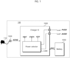
- FIG. 1 is a block diagram showing a mobile device including a charger integrated circuit according to at least one example embodiment of the inventive concepts.
- a mobile device 100 of at least one example embodiment of the inventive concepts may include a charger integrated circuit 1000 and/or a battery 1050, etc., but the example embodiments are not limited thereto, and for example, the mobile device may include a greater or lesser number of constituent components.
- the charger integrated circuit (IC) 1000 may charge the battery 1050 using the input voltage VCHG provided through the power adapter 110.
- the input voltage VCHG may be an alternating current (AC) or a direct current (DC) voltage.
- the charger IC 1000 operates in a buck mode for charging the battery 1050 by switching the input voltage VCHG provided through the power adapter 110, but the example embodiments are not limited thereto.
- the charger IC 1000 may charge the battery 1050 using the charging voltage CHGVL obtained by converting the input voltage VCHG and/or may provide the load voltage VSYS. According to at least one example embodiment, when the power adapter 110 is removed, the charger IC 1000 may output the load voltage VSYS to one or more internal components of the mobile device 100 using the battery voltage VBAT provided from the battery 1050, but the example embodiments are not limited thereto, and for example, the charger IC 1000 may output the load voltage VSYS while the power adapter 110 is connected to the charging terminal 1030 and/or the power adapter 110 is providing the input voltage VCHG to the charger IC 1000, etc.
- the charger IC 1000 includes the power selector 1200 to perform the above-described voltage and/or power selection functions.
- the power selector 1200 selects the highest voltage among, e.g., the battery voltage VBAT, the charging voltage CHGVL, and/or the load voltage VSYS, but is not limited thereto.
- the power selector 1200 may provide the selected voltage as an external and/or internal power supply voltage.
- the power selector 1200 provides the selected voltage as, for example, a first chip voltage PVDD for use as chip power of the charger IC 1000 and/or a second chip voltage AVDD for driving analog circuits, etc., but the example embodiments are not limited thereto, and for example, the selected voltage may be provided for a single chip voltage or three or more than chip voltages, etc.
- a ground short test is desired and/or required for the plurality of chip voltages, e.g., first chip voltage PVDD and/or the second chip voltage AVDD, etc.
- the ground short test is a test to verify the characteristics of short current generated when the first chip voltage PVDD output terminal and/or the second chip voltage AVDD output terminal is grounded, and/or to verify the protection capability of the charger integrated circuit 1000, but is not limited thereto.
- the power selector 1200 of at least one example embodiment of the inventive concepts may limit a current level of a short circuit current (e.g., the current of the internal power supply voltage) generated during the ground short test for the first chip voltage PVDD output terminal and/or the second chip voltage AVDD output terminal, etc.
- a short circuit current e.g., the current of the internal power supply voltage
- the power selector 1200 may protect internal elements and/or components of the mobile device 100 and/or the charger IC 1000 from impact and/or damage due to overcurrent from the internal power supply voltage.
- the power selector 1200 may continuously supply an internal power supply voltage (not shown, VDDX) capable of driving internal circuits even when the levels of the first chip voltage PVDD and the second chip voltage AVDD drop sharply.
- the charger IC 1000 may normally perform internal control functions and/or operations.
- the charger integrated circuit 1000 of at least one example embodiment of the inventive concepts includes the power selector 1200 which is capable of limiting the overcurrent generated by the internal power supply voltage during the ground short test.
- the power selector 1200 selects at least one voltage among the battery voltage VBAT, the charging voltage CHGVL, and the load voltage VSYS, etc., for example, the power selector 1200 may select a highest voltage among the battery voltage VBAT, the charging voltage CHGVL, and the load voltage VSYS, etc., but is not limited thereto, and supplies the selected voltage to the internal power supply voltage VDDX node.
- the internal power supply voltage VDDX node may be separated from the chip voltage (e.g., PVDD, AVDD) nodes through a back-to-back diode-structured power switch (e.g., a short circuit protection transistor).
- the power selector 1200 may generate a current control signal for limiting the size and/or amount of the short circuit current by detecting the voltage drop of the chip voltage (e.g., PVDD, AVDD) nodes during the performance of the ground short test.
- the gate voltage of the power switch may be controlled using the current control signal generated by the power transistors to limit the amount of overcurrent generated by the internal power supply voltage during the ground short test a desired and/or certain level.
- the structure and function of the power selector 1200 for limiting the overcurrent of the internal power supply voltage will be described in detail through the drawings to be described later.
- FIG. 2 is a block diagram showing the configuration of the charger integrated circuit of at least one example embodiments of the inventive concepts.
- the charger IC 1000 may include a low-dropout (LDO) regulator 1100 and/or a power selector 1200, etc., but is not limited thereto.
- the power selector 1200 may include a power drop sensor 1220 and/or a short current limiter 1240, etc., but is not limited thereto.
- the LDO regulator 1100 converts the input voltage VCHG provided from the power adapter 110 (see, e.g., FIG. 1 ) into a stable charging voltage CHGVL.
- the LDO regulator 1100 features and/or causes a low voltage drop between an input voltage VCHG and a charge voltage CHGVL corresponding to the output. Therefore, the LDO regulator 1100 is a linear regulator with little ripple of the charging voltage CHGVL.
- the LDO regulator 1100 according to at least one example embodiment is just one example of a converter for providing a stable level of charging voltage CHGVL, and various regulators and/or converters may be used to provide a charging voltage CHGVL according to other example embodiments.
- the power selector 1200 selects a voltage (such as the highest voltage) among a plurality of potential chip voltages, e.g., the battery voltage VBAT, the charging voltage CHGVL, and/or the load voltage VSYS, etc., and provides it as chip voltages AVDD and/or PVDD, etc.
- the power selector 1200 may limit the size and/or amount of a short circuit current generated by the internal power supply voltage during a ground short test operation for the first chip voltage PVDD and/or the second chip voltage AVDD, etc.
- a pad P1 of the test board to which the first chip voltage PVDD is transmitted may be connected to the ground GND, but the example embodiments are not limited thereto.
- the power selector 1200 may detect a drop in the level of the first chip voltage PVDD that occurs during the ground short test and may limit the size, magnitude, and/or amount of the first short circuit current Isp to a desired and/or predetermined level.
- the power selector 1200 may detect a drop in the level of the second chip voltage AVDD and limit the level of the second short circuit current Isa even during the ground short test operation for the second chip voltage AVDD.
- the power selector 1200 includes a power drop sensor 1220 to monitor the voltage levels of the chip voltages PVDD and/or AVDD and detect a drop in the voltage level of the chip voltages PVDD and/or AVDD, etc.
- the power selector 1200 may include a short current limiter 1240 for limiting the size, magnitude, and/or amount of the first short circuit current Isp and/or the second short circuit current Isa using a detection result of the power drop sensor 1220, but the example embodiments are not limited thereto.
- the power selector 1200 and/or the power drop sensor 1220, etc. may be implemented as processing circuitry.
- the processing circuitry may include hardware or hardware circuit including logic circuits; a hardware/software combination such as a processor executing software and/or firmware; or a combination thereof.
- the processing circuitry more specifically may include, but is not limited to, a central processing unit (CPU), an arithmetic logic unit (ALU), a digital signal processor, a microcomputer, a field programmable gate array (FPGA), a System-on-Chip (SoC), a programmable logic unit, a microprocessor, application-specific integrated circuit (ASIC), etc., but is not limited thereto.
- CPU central processing unit
- ALU arithmetic logic unit
- FPGA field programmable gate array
- SoC System-on-Chip
- ASIC application-specific integrated circuit
- the power drop sensor 1220 may activate or deactivate the current limiting function of the short current limiter 1240 by detecting a level drop of the chip voltages PVDD and/or AVDD, etc., or in other words, the power drop sensor 1220 may control the short current limiter 1240 based on a detected voltage level drop of the monitored at least one of chip voltage PVDD and/or AVDD, etc. For example, when the power drop sensor 1220 detects and/or determines that the monitored level of the first chip voltage PVDD and/or the second chip voltage AVDD is greater than or equal to a desired reference voltage, the power drop sensor 1220 deactivates (e.g., turns off) the current limiting function of the short current limiter 1240.
- the power drop sensor 1220 sets the power switch that switches the first chip voltage PVDD and/or the second chip voltage AVDD of the short current limiter 1240 to a fully turn-on mode (e.g., a normal operation mode, etc.).
- the power drop sensor 1220 controls the short current limiter 1240 by generating and/or transmitting a current control signal CTRL_SCL to the short current limiter 1240 based on the detected level drop of the chip voltages PVDD and/or AVDD, etc.
- the power drop sensor 1220 activates (e.g., turns on) the current limiting function of the short current limiter 1240 using the current control signal CTRL_SCL in response to the power drop sensor 1220 detecting and/or determining that the level of the first chip voltage PVDD and/or the second chip voltage AVDD is lower than the desired reference voltage.
- the power drop sensor 1220 is driven using an internal power supply voltage VDDX provided through a node separated from a node where the chip voltages AVDD and/or PVDD are formed.
- the power drop sensor 1220 stably uses a separate internal power supply voltage VDDX from the chip voltages AVDD and/or PVDD even if the chip voltages AVDD and/or PVDD drop during the ground short test operation. Accordingly, the power drop sensor 1220 may stably generate the current control signal CTRL_SCL without being affected by level changes of chip voltages AVDD and PVDD, etc.
- the short current limiter 1240 may limit the first short circuit current Isp and/or the second short circuit current Isa according to and/or based on the current control signal CTRL_SCL provided by the power drop sensor 1220.
- the short current limiter 1240 may transfer the internal power supply voltage VDDX to a first chip voltage node for providing the first chip voltage PVDD through a first short circuit protection transistor (not shown).
- the short current limiter 1240 transfers the internal power supply voltage VDDX to the second chip voltage node for providing the second chip voltage AVDD through a second short circuit protection transistor (not shown).
- the first and second short circuit protection transistors are driven in a turned-on state during the normal mode (e.g., a first mode, a first operation mode, etc.).
- the first and second short circuit protection transistors are driven in a saturation mode (e.g., a second mode, a second operation mode, a test mode, etc.). Therefore, during the ground short test, the magnitude, size, level, and/or amount of the first short circuit current Isp and/or the second short circuit current Isa flowing through the first short circuit protection transistor and/or the second short circuit protection transistor may be limited and/or decreased, thereby protecting the internal components of the mobile device 100 and/or the charger IC 1000 from damage from an overcurrent, etc.
- a saturation mode e.g., a second mode, a second operation mode, a test mode, etc.
- the battery 1050 may be built into and/or connected to the mobile device 100, but the example embodiments are not limited thereto, and for example, the battery 1050 may be omitted and the mobile device 100 may be driven directly by the power adapter 110, etc. In at least one example embodiment, the battery 1050 may be detachable from the mobile device 100.
- the battery 1050 may include one or a plurality of battery cells. A plurality of battery cells may be connected in series and/or parallel.
- the charger integrated circuit 1000 includes the power selector 1200 operable even when the chip voltage (e.g., AVDD and/or PVDD) drops during the ground short test. Accordingly, the charger integrated circuit 1000 may limit and/or decrease an overcurrent due to a short circuit during the ground short test operation and/or if a short circuit develops during a normal charging operation (e.g., a non-test operation) of the mobile device 100 using a power adapter 110, etc.
- the chip voltage e.g., AVDD and/or PVDD
- the charger integrated circuit 1000 may limit and/or decrease an overcurrent due to a short circuit during the ground short test operation and/or if a short circuit develops during a normal charging operation (e.g., a non-test operation) of the mobile device 100 using a power adapter 110, etc.
- the power selector 1200 may separate the internal power supply voltage (e.g., VDDX) node from the output voltage (e.g., PVDD, AVDD) nodes through a short circuit protection transistor having a back-to-back diode structure, but is not limited thereto.
- the power selector 1200 may detect the voltage drop of the chip voltage nodes PVDD and/or AVDD to generate the current control signal CTRL_SCL for limiting the size, level, amount, magnitude, and/or duration of the short circuit current.
- the power selector 1200 may limit the size, level, magnitude, amount, and/or duration of overcurrent generated during the ground short test and/or during normal operation of the mobile device 100, etc.
- FIG. 3 is a circuit diagram briefly showing the structure of the power selector of FIG. 2 according to some example embodiments.
- the power selector 1200 includes a plurality of power transistors, e.g., power transistors M1, M2, and M3, etc., a maximum voltage selector 1210 (e.g., a voltage detector, a chip voltage selector, etc.), a power drop sensor 1220, and/or a short current limiter 1240, etc., but the example embodiments are not limited thereto.
- the power transistors M1, M2, and M3 respectively switch the battery voltage VBAT, the charging voltage CHGVL, and/or the load voltage VSYS, etc., according to and/or based on the control of the maximum voltage selector 1210.
- the first power transistor M1 switches the battery voltage VBAT and transfers it to the internal power supply voltage VDDX node.
- the first power transistor M1 may be implemented as, for example, a PMOS transistor, but is not limited thereto.
- the source of the first power transistor M1 is connected to the battery voltage VBAT and the drain of the first power transistor M1 is connected to the internal power voltage VDDX node, but is not limited thereto.
- the first power transistor M1 may include a body diode BD1 corresponding to a parasitic diode of the PMOS transistor, but is not limited thereto. A leakage current that may occur when the first power transistor M1 is turned off may be blocked by the body diode BD1, etc.
- the second power transistor M2 switches the load voltage VSYS and transfers it to the internal power voltage VDDX node.
- the second power transistor M2 may also be implemented as a PMOS transistor, but is not limited thereto.
- the source of the second power transistor M2 is connected to the load voltage VSYS and the drain of the second power transistor M2 is connected to the internal power supply voltage VDDX node, but is not limited thereto.
- a body diode BD2 is also formed in the second power transistor M2, but is not limited thereto. A leakage current that may occur when the second power transistor M2 is turned off may be blocked by the body diode BD2, etc.
- the third power transistor M3 switches the charging voltage CHGVL and transfers it to the internal power supply voltage VDDX node.
- the third power transistor M3 may also be implemented as a PMOS transistor, but is not limited thereto.
- the source of the third power transistor M3 is connected to the charging voltage CHGVL and the drain of the third power transistor M3 is connected to the internal power supply voltage VDDX node, but is not limited thereto.
- the third power transistor M3 may also block leakage current that may occur in a turn-off state by the body diode BD3, etc.
- the power transistors M1, M2, and M3 are implemented as PMOS transistors, but the example embodiments of the inventive concepts are not limited thereto.
- one or more of the power transistors M1, M2, and M3 may be implemented as an NMOS transistor, but the example embodiments are not limited thereto, and for example, the power transistors may be implemented as non-MOSFET transistors, etc.
- each of the power transistors M1, M2, and M3 may be implemented in a form in which a plurality of PMOS transistors and/or NMOS transistors are cascaded, etc.
- the maximum voltage selector 1210 compares the respective levels of the battery voltage VBAT, the charging voltage CHGVL, and the load voltage VSYS, and selects, for example, the voltage with the highest voltage level, but the example embodiments are not limited thereto, and for example, the maximum voltage selector 1210 may select a voltage above a desired threshold voltage level, etc., select each of the voltages in sequential order, select the voltages in random order, select the voltages on a periodic basis, select the voltage based on user input, etc.
- the maximum voltage selector 1210 controls the power transistors M1, M2, and M3 to transmit the highest-level voltage among the battery voltage VBAT, the charging voltage CHGVL, and the load voltage VSYS to the internal power supply voltage VDDX node, but the example embodiments are not limited thereto.
- the maximum voltage selector 1210 turns off the first and second power transistors M1 and M2 and turns on the third power transistor M3, but the example embodiments are not limited thereto.
- the power drop sensor 1220 monitors the levels of the chip voltages PVDD and/or AVDD and generates a current control signal CTRL_SCL according to and/or based on the monitoring result.
- the power drop sensor 1220 uses the internal power supply voltage VDDX as a power source to monitor the level drop of the chip voltages PVDD and/or AVDD.
- the power drop sensor 1220 generates a current control signal CTRL_SCL for activating the short circuit current limiting function of the short current limiter 1240 when at least one of the chip voltages PVDD and AVDD drops below the reference voltage VREF, but the example embodiments are not limited thereto.
- the power drop sensor 1220 is driven by using the internal power supply voltage VDDX provided as a node separate from the nodes for the chip voltages PVDD and AVDD during the ground short test, but is not limited thereto. Accordingly, even in a state where the chip voltages PVDD and/or AVDD rapidly decrease due to the ground short test, the power drop sensor 1220 may continue and/or maintain monitoring of the chip voltages PVDD and/or AVDD and provide overcurrent limiting functions, etc.
- the short current limiter 1240 includes a plurality of short circuit protection transistors 1241, but is not limited thereto.
- the plurality of short circuit protection transistors 1241 includes a first short circuit protection transistor SPT1 that provides the internal power supply voltage VDDX as the first chip voltage PVDD in a normal mode.
- the plurality of short circuit protection transistors 1241 include a second short circuit protection transistor SPT2 that provides the internal power supply voltage VDDX as the second chip voltage AVDD in a normal mode, but the example embodiments are not limited thereto.
- the first and second short circuit protection transistors SPT1 and SPT2 are controlled by the voltage formed at the first node N1, but are not limited thereto.
- the power drop sensor 1220 generates a high level 'H' current control signal CTRL_SCL.
- the high level 'H' current control signal CTRL_SCL turns off the transistor M5 of the short current limiter 1240.
- the transistor M6 maintains a turned-on state by the internal power supply voltage VDDX, and the voltage of the first node N1 maintains the ground voltage level.
- the first and second short circuit protection transistors SPT1 and SPT2 maintain a turned-on state, and the internal power supply voltage VDDX is provided as the first chip voltage PVDD and/or the second chip voltage AVDD, but the example embodiments are not limited thereto.
- the output terminal of the first chip voltage PVDD and/or the second chip voltage AVDD is grounded. Accordingly, the level of the first chip voltage PVDD and/or the second chip voltage AVDD becomes lower than the reference voltage VREF. Then, the power drop sensor 1220 generates a low level 'L' current control signal CTRL_SCL based on detecting the voltage drop in the first chip voltage PVDD and/or the second chip voltage AVDD. Transistor M5 of the short current limiter 1240 is turned on as the low level 'L' current control signal CTRL_SCL is provided. Accordingly, a current path in which the internal power supply voltage VDDX is grounded via the diode-connected transistor M4 and M5, the resistor Rs, and the transistor M6 is formed, but the example embodiments are not limited thereto.
- Gate voltages of the first short circuit protection transistor SPT1 and/or the second short circuit protection transistor SPT2 are built up at the first node N1 by the resistor Rs present in the current path formed between the internal power supply voltage VDDX node and the ground node, but the example embodiments are not limited thereto. Therefore, during normal operation, the first short circuit protection transistor SPT1 and the second short circuit protection transistor SPT2 maintain a turned-on state. However, during the ground short test operation and/or during a short circuit event during normal operation, the first short circuit protection transistor SPT1 and/or the second short circuit protection transistor SPT2 is operated in the saturation mode by the gate voltage formed at the first node N1, but is not limited thereto.
- the level of the gate-source voltage Vgs of the first short circuit protection transistor SPT1 and/or the second short circuit protection transistor SPT2 may be controlled by selecting the size of the resistor Rs.
- the saturation current of the first short circuit protection transistor SPT1 and/or the second short circuit protection transistor SPT2 may be adjusted by adjusting the level of the gate-source voltage Vgs.
- the magnitude of the short circuit current flowing through the first short circuit protection transistor SPT1 and/or the second short circuit protection transistor SPT2 operating in the saturation mode may be controlled by the short current limiter 1240.
- the plurality of transistors M4, M5, and M6 and/or the resistor Rs forming a current path between the internal power supply voltage VDDX node and the ground node may be referred to as a gate control circuit 1243, but the example embodiments are not limited thereto. This is because the gate voltage of the first short circuit protection transistor SPT1 and/or the second short circuit protection transistor SPT2 may be controlled by the transistors M4, M5, and M6 and the resistor Rs, etc.
- the method of limiting the short circuit current performed during the ground short test operation and/or during a short circuit event during normal operation of the power selector 1200 has been described.
- the first short circuit protection transistor SPT1 and/or the second short circuit protection transistor SPT2 of the short circuit current limiter 1240 operates in saturation mode by the current control signal CTRL_SCL generated by the power drop sensor 1220.
- the short circuit current flowing through these transistors may be limited to the saturation current level by the first short circuit protection transistor SPT1 and/or the second short circuit protection transistor SPT2 operating in the saturation mode, etc.
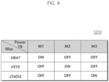
- FIG. 4 is a table showing the function of the maximum voltage selector of FIG. 3 according to some example embodiments.
- the maximum voltage selector 1210 selects the highest one among the battery voltage VBAT, the charging voltage CHGVL, and the load voltage VSYS, and provides it as the internal power supply voltage VDDX, but the example embodiments are not limited thereto.
- the maximum voltage selector 1210 turns on the first power transistor M1 when it is determined that the battery voltage VBAT is the highest among the power supply voltages VBAT, VSYS, and CHGVL, but the example embodiments are not limited thereto. Further, the maximum voltage selector 1210 turns off the second and third power transistors M2 and M3 when it is determined that the battery voltage VBAT is the highest. Accordingly, the battery voltage VBAT is transferred to the internal power voltage VDDX node by the first power transistor M1.
- the maximum voltage selector 1210 turns off the first and third power transistors M1 and M3 and turns on the second power transistor M2. Then, the load voltage VSYS is transferred to the internal power voltage VDDX node by the second power transistor M2.
- the maximum voltage selector 1210 turns off the first and second power transistors M1 and M2, and turns on the third power transistor M3. Then, the charging voltage CHGVL is transferred to the internal power voltage VDDX node by the third power transistor M3.
- the function of the maximum voltage selector 1210 for providing the highest voltage among power supply voltages as the internal power supply voltage VDDX has been briefly described, but the example embodiments are not limited thereto.
- the highest voltage selection function of the maximum voltage selector 1210 described through the table may be implemented through various comparators, logic circuits, and/or processing circuitry, etc., but is not limited thereto.
- FIG. 5 is a circuit diagram showing an example configuration of the power drop sensor of FIG. 3 according to some example embodiments.
- the power drop sensor 1220 includes a plurality of comparators, e.g., comparators 1221 and 1222, etc., that monitor chip voltages AVDD and/or PVDD and detect level changes of chip voltages AVDD and/or PVDD, a plurality of inverters, e.g., inverters INV1 and INV2, etc., and/or a plurality of level detectors, e.g., level detectors 1223, 1224, etc., and/or an AND gate 1225, but the example embodiments are not limited thereto.
- the power drop sensor 1220 is driven using an internal power supply voltage VDDX managed as a node separated from nodes of the chip voltages AVDD and PVDD which are grounded during a ground short test, etc.
- a reference resistor Rref and a reference current source Iref are provided to generate the reference voltage VREF of the comparators 1221 and 1222 using the internal power supply voltage VDDX, but the example embodiments are not limited thereto.
- the internal power supply voltage VDDX is divided by the reference resistor Rref and the current source Iref to generate the reference voltage VREF.
- the reference resistor Rref and reference current source Iref are adjusted to divide the internal supply voltage VDDX to provide a reference voltage VREF of, e.g., 3.5V, but are not limited thereto.
- the first comparator 1221 monitors the level of the first chip voltage PVDD. When the voltage level of the first chip voltage PVDD is equal to or higher than the reference voltage VREF, the first comparator 1221 generates a low level 'L' output signal. Then, the first inverter INV1 inverts the low-level output signal of the first comparator 1221 to generate the high-level first flag signal FLa. On the other hand, when the voltage level of the first chip voltage PVDD is lower than the reference voltage VREF, the first comparator 1221 generates a high level 'H' output signal. Then, the first inverter INV1 inverts the high level output signal of the first comparator 1221 to generate the low level first flag signal Fla.
- the second comparator 1222 monitors the level of the second chip voltage AVDD. When the voltage level of the second chip voltage AVDD is equal to or higher than the reference voltage VREF, the second comparator 1222 generates a low level 'L' output signal. Then, the second inverter INV2 inverts the low level output signal of the second comparator 1222 to generate the high level 'H' second flag signal FLb. On the other hand, when the voltage level of the second chip voltage AVDD is lower than the reference voltage VREF, the second comparator 1222 generates a high level 'H' output signal. Then, the second inverter INV2 inverts the high-level output signal of the second comparator 1222 to generate the low-level second flag signal FLb.
- the first level detector 1223 monitors the level of the first chip voltage PVDD.
- the first level detector 1223 will generate the third flag signal FLc of low level 'L' when the level of the first chip voltage PVDD is lower than the desired and/or predetermined level threshold voltage Vth (e.g., Vth ⁇ VREF).
- Vth e.g., Vth ⁇ VREF
- the first level detector 1223 can be used as an auxiliary means for controlling the level of the short circuit current when the first comparator 1221 and/or the first inverter INV1 do not operate normally due to a failure and/or error, but is not limited thereto.
- the second level detector 1224 monitors the level of the second chip voltage AVDD.
- the second level detector 1224 will generate a fourth flag signal FLd of low level 'L' when the level of the second chip voltage AVDD is lower than the desired and/or predetermined level threshold voltage Vth (e.g., Vth ⁇ VREF).
- Vth e.g., Vth ⁇ VREF
- the second level detector 1224 serves as an auxiliary means for limiting the short circuit current when the second comparator 1222 and the second inverter INV2 do not operate normally.
- the AND gate 1225 generates the current control signal CTRL_SCL by performing an logical AND operation on the first to fourth flag signals FLa, FLb, FLc, and FLd, but is not limited thereto.
- the AND gate 1225 provides a high-level 'H' current control signal CTRL_SCL when the first to fourth flag signals FLa, FLb, FLc, and FLd are all high-level 'H'.
- the AND gate 1225 generates a low-level 'L' current control signal CTRL_SCL when any one of the first to fourth flag signals FLa, FLb, FLc, and FLd is low level 'L'.
- the AND gate 1225 maintains the high level 'H' current control signal CTRL_SCL when both of the voltage levels of the chip voltages AVDD and PVDD are equal to or greater than the reference voltage VREF.
- the AND gate 1225 transitions the current control signal CTRL_SCL to a low level 'L' to activate the current limit function when any one of the levels of the chip voltages AVDD and PVDD is lower than the reference voltage VREF.
- the first comparator 1221 and the first inverter INV1, the second comparator 1222 and the second inverter INV2, and the AND gate 1225 are driven using the internal power supply voltage VDDX as a power source.
- the level detectors 1223 and 1224 may also be driven using the internal power supply voltage VDDX. Accordingly, even when the levels of the chip voltages AVDD and PVDD drop rapidly during the ground short test, the power drop sensor 1220 continues to operate normally.
- FIG. 6 is a timing diagram illustrating a process of generating a current control signal CTRL_SCL by a power drop sensor when a first chip voltage PVDD is short circuited to ground according to at least one example embodiment of the inventive concepts. Referring to FIGs. 5 and 6 , an operation of the power drop sensor 1220 when the first chip voltage PVDD drops rapidly during a ground short test will be described, but the example embodiments are not limited thereto.
- the operating state of the power drop sensor 1220 before the ground short test operation is performed is shown. That is, the chip voltages AVDD and PVDD maintain normal levels (e.g., 4V) higher than the reference voltage VREF, but the example embodiments are not limited thereto. Accordingly, the inverters INV1 and INV2 and the level detectors 1223 and 1224 all output flag signals FLa, FLb, FLc, and FLd of a high level 'H'. As a result, the AND gate 1225 will output the current control signal CTRL_SCL at a high level 'H'. In the high level 'H' state of the current control signal CTRL_SCL, the transistor M5 of the short current limiter 1240 is turned off, and the short circuit protection transistors SPT1 and SPT2 are fully turned on.
- CTRL_SCL In the high level 'H' state of the current control signal CTRL_SCL, the transistor M5 of the short current limiter 1240 is turned off, and the short circuit protection transistors SPT1
- the ground short test operation for the first chip voltage PVDD starts. Then, the voltage level of the second chip voltage AVDD maintains a normal state, but the voltage level of the first chip voltage PVDD starts to fall. However, until the time T2, the voltage levels of both the first chip voltage PVDD and the second chip voltage AVDD are higher than the reference voltage VREF. Accordingly, all of the flag signals FLa, FLb, FLc, and FLd are maintained at a high level 'H'. Accordingly, the AND gate 1225 will output the current control signal CTRL_SCL at a high level 'H'.
- the voltage level of the first chip voltage PVDD becomes lower than the reference voltage VREF.
- the first comparator 1221 will transition the comparison result from the low level 'L' to the high level 'H'.
- the first inverter INV1 will transition the first flag signal FLa from the high level 'H' to the low level 'L'.
- the AND gate 1225 converts the current control signal CTRL_SCL to the low level 'L'.
- the short current limiter 1240 activates the short circuit current limiting operation in response to the low level 'L' transition of the current control signal CTRL_SCL.
- the transistor M5 of the short current limiter 1240 is turned on, and the short circuit protection transistors SPT1 and SPT2 are driven in the saturation mode. Therefore, the short circuit current flowing through the short circuit protection transistors SPT1 and SPT2 is limited and/or decreased to the saturation current level, etc.
- the voltage level of the first chip voltage PVDD becomes lower than the threshold voltage Vth (e.g., level threshold voltage, etc.). Then, the first level detector 1223 that monitors the level of the first chip voltage PVDD will transition the third flag signal FLc from the high level 'H' to the low level 'L'. As two flag signals FLa and FLc among the four flag signals FLa, FLb, FLc, and FLd transition to a low level 'L', the AND gate 1225 generates a low level 'L' current control signal CTRL_SCL. Accordingly, the short current limiter 1240 will continue to limit and/or decrease the short circuit current activated at the time point T2.
- the threshold voltage Vth e.g., level threshold voltage, etc.
- the current control signal CTRL_SCL may transition normally by the first level detector 1223.
- the operation of the power drop sensor 1220 when the first chip voltage PVDD is grounded in the ground short test has been described above.
- the power drop sensor 1220 may activate the short circuit current limitation through the current control signal CTRL_SCL when any one of the voltage levels of the chip voltages AVDD and PVDD is lower than the reference voltage VREF.
- the power drop sensor 1220 is driven by the internal power supply voltage VDDX managed as a node separate from the node of the first chip voltage PVDD. Therefore, monitoring of the chip voltages AVDD and PVDD of the power drop sensor 1220 and generation of the current control signal CTRL_SCL may be improved, increased and/or ensured even during the ground short test, but the example embodiments are not limited thereto.
- FIG. 7 is a timing diagram illustrating a process of generating a current control signal CTRL_SCL by a power drop sensor during a ground short test the second chip voltage AVDD according to at least one example embodiment of the inventive concepts.
- an operation of the power drop sensor 1220 will be described in the case where the first chip voltage PVDD maintains a normal level and the second chip voltage AVDD drops rapidly during the ground short test, but the example embodiments are not limited thereto.
- the period between T0 to T1 of FIG. 7 shows an operating state of the power drop sensor 1220 before the ground short test operation is performed.
- the chip voltages AVDD and PVDD each maintain a normal level higher than the reference voltage VREF.
- the inverters INV1 and INV2 and the level detectors 1223 and 1224 all output flag signals FLa, FLb, FLc, and FLd of a high level 'H'.
- the AND gate 1225 receiving the flag signals FLa, FLb, FLc, and FLd outputs the current control signal CTRL_SCL at a high level 'H'.
- the ground short test operation for the second chip voltage AVDD starts.
- the first chip voltage PVDD and the second chip voltage AVDD are provided to separate nodes through the first short circuit protection transistor SPT1 and the second short circuit protection transistor SPT2, but the example embodiments are not limited thereto. Accordingly, the first chip voltage PVDD maintains a steady state, but the second chip voltage AVDD starts to drop due to being grounded. However, until the time T2, both the first chip voltage PVDD and the second chip voltage AVDD are still higher than the reference voltage VREF. Accordingly, all of the flag signals FLa, FLb, FLc, and FLd are maintained at a high level 'H'. Accordingly, the AND gate 1225 will output the current control signal CTRL_SCL of high level 'H'.
- the voltage level of the second chip voltage AVDD becomes lower than the reference voltage VREF.
- the second comparator 1222 will transition the comparison result from the low level 'L' to the high level 'H'.
- the second inverter INV2 will transition the second flag signal FLb from the high level 'H' to the low level 'L'.
- the AND gate 1225 converts the current control signal CTRL_SCL to the low level 'L'.
- the short current limiter 1240 activates the short circuit current limiting operation in response to the low level 'L' transition of the current control signal CTRL_SCL.
- the transistor M5 of the short current limiter 1240 is turned on, and the short circuit protection transistors SPT1 and SPT2 are driven in the saturation mode. Therefore, the short circuit current flowing through the short circuit protection transistors SPT1 and SPT2 is limited to and/or decreased to the saturation current level.
- the second chip voltage AVDD becomes lower than the threshold voltage Vth (e.g., level threshold voltage, etc.). Then, the second level detector 1224 monitoring the second chip voltage AVDD will transition the fourth flag signal FLd from the high level 'H' to the low level 'L'. As the two flag signals FLb and FLd among the four flag signals FLa, FLb, FLc, and FLd transition to the low level 'L', the AND gate 1225 generates low level 'L' current control signal CTRL_SCL. Accordingly, the short circuit current limiter 1240 will continue to limit and/or decrease the short circuit current activated at the time point T2.
- the threshold voltage Vth e.g., level threshold voltage, etc.
- the power drop sensor 1220 may activate the short circuit current limitation through the current control signal CTRL_SCL when any one of the chip voltages AVDD and PVDD is lower than the reference voltage VREF, etc.
- the power drop sensor 1220 is driven using the internal power supply voltage VDDX managed as a node separated from the second chip voltage AVDD. Therefore, even during the ground short test operation, the function of monitoring the chip voltages AVDD and PVDD of the power drop sensor 1220 and generating the current control signal CTRL_SCL may be increased, improved, and/or guaranteed, etc.
- FIG. 8 is a circuit diagram for explaining the short circuit current limiting operation of the short current limiter according to at least one example embodiment of the inventive concepts.
- an operation of the short current limiter 1240 for limiting the short circuit current during a ground short test for the second chip voltage AVDD will be described, but the example embodiments are not limited thereto.
- the short circuit current limiting operation will be described focusing on the function of the plurality of gate control circuits, e.g., gate control circuits M4, M5, M6, etc., and resistor Rs that control the gate voltage of the second short circuit protection transistor SPT2, but the example embodiments are not limited thereto.
- An operation of the short current limiter 1240 during the ground short test operation for the second chip voltage PVDD is substantially the same as in the ground short test operation for the second chip voltage AVDD and thus description thereof is omitted, but the example embodiments are not limited thereto.
- an output terminal of the second chip voltage AVDD is grounded on the test board, but is not limited thereto.
- the voltage level of the second chip voltage AVDD which is monitored by the power drop sensor 1220, becomes lower than the reference voltage VREF due to the grounding, and the power drop sensor 1220 provides the current control signal CTRL_SCL corresponding to the low level 'L' based the results of the detection of the voltage level drop.
- the PMOS type transistor M5 is turned on. As transistor M5 is turned on, the internal power supply voltage VDDX node is electrically connected to ground via diode-connected transistors M4, M5, resistor Rs, and transistor M6, but is not limited thereto.
- the gate voltage VDDX-Vf of the second short circuit protection transistor SPT2 is formed at the first node N1 by the resistor Rs present on the current path formed between the internal power voltage VDDX node and the ground node, but the example embodiments are not limited thereto.
- the gate-source voltage Vgs of the second short circuit protection transistor SPT2 is controllable by adjusting the size (e.g., the resistance value) of the resistor Rs.
- the operation mode of the second short circuit protection transistor SPT2 is changed from a fully turn-on mode to a saturation mode according to and/or based on the turn-on of the transistor M5. Accordingly, the short circuit current 'Is' flowing through the second short circuit protection transistor SPT2 may be limited and/or decreased to a desired saturation current level.
- the body diode of the power transistor M3 and the body diode of the second short circuit protection transistor SPT2 are connected in a back-to-back fashion, but the example embodiments are not limited thereto. Therefore, current through the parasitic diode is decreased and/or is not generated during the ground short test.
- the short circuit current limiting function of the short current limiter 1240 during the ground short test has been briefly described.
- the first short circuit protection transistor SPT1 and/or the second short circuit protection transistor SPT2 is operated in saturation mode by the current control signal CTRL_SCL generated by the power drop sensor 1220, etc.
- the short circuit current Is flowing through the first short circuit protection transistor SPT1 and/or the second short circuit protection transistor SPT2 is limited and/or decreased to the level of the saturation current of these transistors, etc.
- FIG. 9 is an example waveform diagram of a charger integrated circuit according to at least one example embodiment of the inventive concepts. Referring to FIG. 9 , it is assumed that the battery voltage VBAT is selected as the power supply voltage supplied as the internal power voltage VDDX, but the example embodiments are not limited thereto.
- the second chip voltage AVDD maintains the same and/or similar voltage level (e.g., within +/- 10%, etc.) to the battery voltage VBAT, but is not limited thereto.
- the level (e.g., the logic level, etc.) of the current control signal CTRL_SCL provided from the power drop sensor 1220 maintains the high level 'H' (e.g., high logic level, etc.).
- the transistor M5 is turned off, and the voltage of the first node N1 and/or the gate voltage Vgate of the second short circuit protection transistor SPT2 is at the ground level (e.g., approximately 0V, etc.).
- the battery current IBAT that supplies the battery voltage VBAT is small enough to be negligible (e.g., approximately 0 mA, etc.), but the example embodiments are not limited thereto.
- the ground short test starts (Short On). That is, for example, the second chip voltage AVDD terminal is connected to ground, but the example embodiments are not limited thereto. Then, the voltage level of the second chip voltage AVDD, which is monitored by the power drop sensor 1220, starts to drop rapidly due to the connection to ground. As the voltage level of the second chip voltage AVDD drops, the battery current IBAT starts to increase rapidly. At this time, the battery current IBAT may rapidly increase to 2A or more.
- the power drop sensor 1220 transitions the current control signal CTRL_SCL to a low level 'L' (e.g., low logic level) based on the detection of the voltage level drop of the second chip voltage AVDD, but is not limited thereto.
- the transistor M5 receiving the current control signal CTRL_SCL as a gate voltage is turned on.
- the transistor M5 is turned on, the voltage of the first node N1 and/or the gate voltage Vgate of the second short circuit protection transistor SPT2 transitions to a high level 'H'.
- the second short circuit protection transistor SPT2 operates in a saturation mode, etc.
- the short circuit current flowing through the second short circuit protection transistor SPT2 is limited and/or decreased to the saturation current level, etc.
- the battery current IBAT flowing through the battery may return to a normal state (e.g., 0 mA), but the example embodiments are not limited thereto.
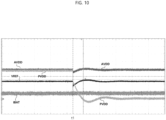
- FIG. 10 is a graph showing a result of a ground short test for a first chip voltage PVDD of a charger integrated circuit according to at least one example embodiment of the inventive concepts. Referring to FIG. 10 , it may be confirmed that the battery current IBAT may be stably limited and/or decreased even if the level of the first chip voltage PVDD drops rapidly due to a short circuit, etc., but the example embodiments are not limited thereto.
- the ground short test (e.g., ground short test operation, short circuit test operation, etc.) for the first chip voltage PVDD starts.
- the first chip voltage PVDD and/or the second chip voltage AVDD are provided to separated nodes through the first short circuit protection transistor SPT1 and the second short circuit protection transistor SPT2, but the example embodiments are not limited thereto. Accordingly, even when the first chip voltage PVDD is grounded, the second chip voltage AVDD may maintain a normal state, but the example embodiments are not limited thereto.
- the first chip voltage PVDD which is monitored by the power drop sensor 1220, becomes lower than the reference voltage VREF (e.g., desired voltage, etc.) at time 11.
- the power drop sensor 1220 outputs the current control signal CTRL_SCL at a low level 'L'.
- the transistor M5 of the short current limiter is turned on, and the first short circuit protection transistor SPT1 operates in a saturation mode.
- the saturation mode operation of the first short circuit protection transistor SPT1 the short circuit current is limited and/or decreased, and the battery current IBAT of the battery supplying the battery voltage VBAT may be restored (e.g., returned to a normal level of current, a desired level of current, etc.).
- the change and/or recovery of the battery current IBAT shown may be so minor that it is hidden in the ripples, etc.
- FIG. 11 is a graph showing a result of a ground short test for the second chip voltage AVDD of the charger integrated circuit according to at least one example embodiment of the inventive concepts. Referring to FIG. 11 , it may be confirmed that the battery current IBAT may be stably limited and/or decreased even when the level of the second chip voltage AVDD decreases and/or rapidly decreases.
- the ground short test operation for the second chip voltage AVDD starts.
- the first chip voltage PVDD and/or the second chip voltage AVDD are provided to separate nodes through the first short circuit protection transistor SPT1 and/or the second short circuit protection transistor SPT2, etc. Accordingly, even when the second chip voltage AVDD is grounded, the first chip voltage PVDD may maintain a normal state, but the example embodiments are not limited thereto.
- the second chip voltage AVDD which is monitored by the power drop sensor 1220, becomes lower than the reference voltage VREF (e.g., the desired voltage level, a reference threshold voltage level, etc.) at time t1.
- the power drop sensor 1220 outputs the current control signal CTRL_SCL at a low level 'L'.
- the transistor M5 of the short current limiter is turned on, and the second short circuit protection transistor SPT2 operates in a saturation mode.
- the short circuit current is limited and/or decreased, and the battery current IBAT of the battery supplying the battery voltage VBAT may be restored (e.g., returned to a normal level, returned to a desired level, etc.).
- the change and/or recovery of the battery current IBAT shown may be so minor that it is hidden in the ripples, but the example embodiments are not limited thereto.
- FIG. 12 is a block diagram showing a power system of a mobile device according to at least one example embodiment of the inventive concepts.
- a power system 2000 may include a battery charging IC 2100 and/or a battery 2300, etc., but is not limited thereto, and for example, may include a greater or lesser number of constituent components.
- the battery charger IC 2100 includes the power selector 2150 of at least one example embodiment of the inventive concepts.
- the power selector 2150 may limit a short circuit current generated during a ground short test operation for the first chip voltage PVDD and/or the second chip voltage AVDD, but is not limited thereto, and for example, the power selector 2150 may further limit a short circuit current generated during normal operation of the battery charger IC 2100 and/or the power system 2000, etc.
- the power selector 2150 may protect internal elements and/or components of the mobile device from impact and/or damage due to overcurrent, etc.
- the power selector 2150 may continuously supply an internal power supply voltage (not shown, VDDX) capable of driving internal circuits even when the first chip voltage PVDD and/or the second chip voltage AVDD are grounded. Therefore, even if the ground short test is performed for the first chip voltage PVDD and/or the second chip voltage AVDD, the power selector 2150, power system 2000, and the mobile device may normally perform internal functions and/or operations, etc.
- Configuration and operations of the battery charger IC 2100 may operate as described in FIGs. 1 to 11 , but is not limited thereto.
- the battery charger IC 2100 may provide a stable voltage to other components of the mobile electronic device.
- each of at least one processor 2400, an input/output interface 2500, a buffer memory 2600, a storage 2700, a display 2800, and/or a communication module 2900 (e.g., communication interface, communication radio, etc.), etc., included in a mobile electronic device may operate using the stable voltage provided from the power management IC 2200.
- the charger IC 2100, the at least one processor 2400, the input/output interface 2500, the buffer memory 2600, the storage 2700, and/or the communication module 2900, etc. may be implemented as processing circuitry.
- the processing circuitry may include hardware or hardware circuit including logic circuits; a hardware/software combination such as a processor executing software and/or firmware; or a combination thereof.
- the processing circuitry more specifically may include, but is not limited to, a central processing unit (CPU), an arithmetic logic unit (ALU), a digital signal processor, a microcomputer, a field programmable gate array (FPGA), a System-on-Chip (SoC), a programmable logic unit, a microprocessor, application-specific integrated circuit (ASIC), etc., but is not limited thereto.
- CPU central processing unit
- ALU arithmetic logic unit
- FPGA field programmable gate array
- SoC System-on-Chip
- ASIC application-specific integrated circuit
- the battery charger IC 2100 may be implemented as an integrated circuit chip and/or as circuitry, etc.
- the battery charger IC 2100 may be mounted using various types of semiconductor packages.
- the battery charger IC 2100 may be mounted using at least one of Package on Package (PoP), Ball Grid Arrays (BGAs), Chip Scale Packages (CSPs), Plastic Leaded Chip Carrier (PLCC), Plastic Dual In-line Package (PDIP), Die in Waffle Pack, Die in Wafer Form, COB (Chip On Board), CERDIP (Ceramic Dual In-line Package), MQFP (Metric Quad Flat Pack), TQFP (Thin Quad Flat Pack), SOIC (Small Outline Integrated Circuit), SSOP (Shrink Small Outline Package), TSOP (Thin Small Outline Package), SIP (System In Package), MCP (Multi Chip Package), WFP (Wafer-level Fabricated Package), WSP (Wafer-Level Processed Stack Package), etc., but is not limited thereto.
- PoP Package on Package
- inventive concepts may include simple design changes or easily changeable aspects of the example embodiments.
- inventive concepts will include techniques that may be easily modified and implemented using the example embodiments. Therefore, the scope of the inventive concepts should not be limited to the above-described example embodiments.
Landscapes
- Engineering & Computer Science (AREA)
- Power Engineering (AREA)
- Physics & Mathematics (AREA)
- General Physics & Mathematics (AREA)
- Charge And Discharge Circuits For Batteries Or The Like (AREA)
- Protection Of Static Devices (AREA)
- Semiconductor Integrated Circuits (AREA)
Applications Claiming Priority (1)
| Application Number | Priority Date | Filing Date | Title |
|---|---|---|---|
| KR1020230020733A KR20240127685A (ko) | 2023-02-16 | 2023-02-16 | 단락 보호 회로를 포함하는 충전 집적 회로 및 그것의 접지 단락 테스트 방법 |
Publications (2)
| Publication Number | Publication Date |
|---|---|
| EP4418481A2 true EP4418481A2 (de) | 2024-08-21 |
| EP4418481A3 EP4418481A3 (de) | 2024-09-25 |
Family
ID=88697791
Family Applications (1)
| Application Number | Title | Priority Date | Filing Date |
|---|---|---|---|
| EP23208023.4A Pending EP4418481A3 (de) | 2023-02-16 | 2023-11-06 | Ladegerät-ic mit kurzschlussschutzschaltung und erdungskurzschlusstestverfahren dafür |
Country Status (4)
| Country | Link |
|---|---|
| US (1) | US20240283261A1 (de) |
| EP (1) | EP4418481A3 (de) |
| KR (1) | KR20240127685A (de) |
| CN (1) | CN118508543A (de) |
Cited By (1)
| Publication number | Priority date | Publication date | Assignee | Title |
|---|---|---|---|---|
| CN119881578A (zh) * | 2025-02-24 | 2025-04-25 | 重庆邮电大学 | 用于功率mosfet性能评估的自动测试装置与方法 |
Families Citing this family (1)
| Publication number | Priority date | Publication date | Assignee | Title |
|---|---|---|---|---|
| US20230398881A1 (en) * | 2022-06-10 | 2023-12-14 | Dr. Ing. H.C. F. Porsche Aktiengesellschaft | Method and control device for operating a charger for electrically driven vehicles and charger |
Family Cites Families (3)
| Publication number | Priority date | Publication date | Assignee | Title |
|---|---|---|---|---|
| US6130813A (en) * | 1999-01-11 | 2000-10-10 | Dell U.S.A., L.P. | Protection circuit for electronic devices |
| TWI247469B (en) * | 2003-02-11 | 2006-01-11 | O2Micro Int Ltd | Power supply system, electronic device comprising the same, and method of ensuring safe operation of batteries in parallel |
| CN113555943B (zh) * | 2021-09-17 | 2022-01-18 | 上海南麟电子股份有限公司 | 一种线性充电升压芯片 |
-
2023
- 2023-02-16 KR KR1020230020733A patent/KR20240127685A/ko active Pending
- 2023-09-01 US US18/459,957 patent/US20240283261A1/en active Pending
- 2023-11-02 CN CN202311445770.2A patent/CN118508543A/zh active Pending
- 2023-11-06 EP EP23208023.4A patent/EP4418481A3/de active Pending
Cited By (1)
| Publication number | Priority date | Publication date | Assignee | Title |
|---|---|---|---|---|
| CN119881578A (zh) * | 2025-02-24 | 2025-04-25 | 重庆邮电大学 | 用于功率mosfet性能评估的自动测试装置与方法 |
Also Published As
| Publication number | Publication date |
|---|---|
| CN118508543A (zh) | 2024-08-16 |
| US20240283261A1 (en) | 2024-08-22 |
| KR20240127685A (ko) | 2024-08-23 |
| EP4418481A3 (de) | 2024-09-25 |
Similar Documents
| Publication | Publication Date | Title |
|---|---|---|
| US11646569B2 (en) | Secondary battery protection circuit, secondary battery protection apparatus and battery pack | |
| EP4418481A2 (de) | Ladegerät-ic mit kurzschlussschutzschaltung und erdungskurzschlusstestverfahren dafür | |
| US9385542B2 (en) | Serial multi-battery charger with independent simultaneous charge and discharge | |
| US8878541B2 (en) | Battery voltage monitoring circuit | |
| US7397221B2 (en) | Battery protection device, battery protection system using the same, and battery protection method | |
| US9081069B2 (en) | Protection IC and method of monitoring a battery voltage | |
| USRE41915E1 (en) | Charge/discharge control circuit and secondary battery | |
| KR100572160B1 (ko) | 이차 전지 충전 회로 | |
| KR102052590B1 (ko) | 배터리 관리 시스템 및 그 구동 방법 | |
| US8415927B2 (en) | Switch embedded integrated circuit and method for battery protection | |
| US20130038131A1 (en) | Semiconductor device to select a power supply | |
| US11146094B2 (en) | Electrical apparatus | |
| JP6072503B2 (ja) | エネルギーハーベスタシステム | |
| US5608385A (en) | Device for determining state of electricity generation of solar battery | |
| US11146081B2 (en) | Circuit device, control device, power receiving device, and electronic device | |
| US20140361730A1 (en) | Bi-directional switching regulator and control circuit thereof | |
| KR20120086256A (ko) | 출력 회로, 온도 스위치 ic, 및 전지 팩 | |
| JP6070318B2 (ja) | 電圧検出回路及び電子機器 | |
| US9306244B2 (en) | Bidirectional interface circuit and battery management system including the same | |
| CN103036266B (zh) | 过充电防止电路和半导体装置 | |
| CN115498709B (zh) | 供电电路及开关电源变换电路 | |
| US7525282B2 (en) | Battery-operated equipment including a microcomputer | |
| KR100228518B1 (ko) | 충방전제어회로 | |
| US8823328B2 (en) | Charging apparatus that can recharge different types of batteries without overcharging them | |
| Mubdir et al. | Smart charger for sealed lead acid batteries based on parallel port PC interfacing |
Legal Events
| Date | Code | Title | Description |
|---|---|---|---|
| PUAI | Public reference made under article 153(3) epc to a published international application that has entered the european phase |
Free format text: ORIGINAL CODE: 0009012 |
|
| STAA | Information on the status of an ep patent application or granted ep patent |
Free format text: STATUS: REQUEST FOR EXAMINATION WAS MADE |
|
| 17P | Request for examination filed |
Effective date: 20231106 |
|
| AK | Designated contracting states |
Kind code of ref document: A2 Designated state(s): AL AT BE BG CH CY CZ DE DK EE ES FI FR GB GR HR HU IE IS IT LI LT LU LV MC ME MK MT NL NO PL PT RO RS SE SI SK SM TR |
|
| PUAL | Search report despatched |
Free format text: ORIGINAL CODE: 0009013 |
|
| REG | Reference to a national code |
Ref country code: DE Ref legal event code: R079 Free format text: PREVIOUS MAIN CLASS: H02H0001060000 Ipc: H02H0007180000 |
|
| AK | Designated contracting states |
Kind code of ref document: A3 Designated state(s): AL AT BE BG CH CY CZ DE DK EE ES FI FR GB GR HR HU IE IS IT LI LT LU LV MC ME MK MT NL NO PL PT RO RS SE SI SK SM TR |
|
| RIC1 | Information provided on ipc code assigned before grant |
Ipc: H02J 7/00 20060101ALI20240822BHEP Ipc: H02H 3/087 20060101ALI20240822BHEP Ipc: H02H 1/06 20060101ALI20240822BHEP Ipc: H02H 9/02 20060101ALI20240822BHEP Ipc: H02H 7/18 20060101AFI20240822BHEP |
|
| P01 | Opt-out of the competence of the unified patent court (upc) registered |
Free format text: CASE NUMBER: APP_65979/2024 Effective date: 20241213 |