EP4418331A1 - Photovoltaic cell and photovoltaic module - Google Patents
Photovoltaic cell and photovoltaic module Download PDFInfo
- Publication number
- EP4418331A1 EP4418331A1 EP23199616.6A EP23199616A EP4418331A1 EP 4418331 A1 EP4418331 A1 EP 4418331A1 EP 23199616 A EP23199616 A EP 23199616A EP 4418331 A1 EP4418331 A1 EP 4418331A1
- Authority
- EP
- European Patent Office
- Prior art keywords
- photovoltaic cell
- along
- busbars
- photovoltaic
- passivation layer
- Prior art date
- Legal status (The legal status is an assumption and is not a legal conclusion. Google has not performed a legal analysis and makes no representation as to the accuracy of the status listed.)
- Pending
Links
Images


Classifications
-
- H—ELECTRICITY
- H10—SEMICONDUCTOR DEVICES; ELECTRIC SOLID-STATE DEVICES NOT OTHERWISE PROVIDED FOR
- H10F—INORGANIC SEMICONDUCTOR DEVICES SENSITIVE TO INFRARED RADIATION, LIGHT, ELECTROMAGNETIC RADIATION OF SHORTER WAVELENGTH OR CORPUSCULAR RADIATION
- H10F19/00—Integrated devices, or assemblies of multiple devices, comprising at least one photovoltaic cell covered by group H10F10/00, e.g. photovoltaic modules
- H10F19/90—Structures for connecting between photovoltaic cells, e.g. interconnections or insulating spacers
- H10F19/902—Structures for connecting between photovoltaic cells, e.g. interconnections or insulating spacers for series or parallel connection of photovoltaic cells
- H10F19/904—Structures for connecting between photovoltaic cells, e.g. interconnections or insulating spacers for series or parallel connection of photovoltaic cells characterised by the shapes of the structures
-
- H—ELECTRICITY
- H10—SEMICONDUCTOR DEVICES; ELECTRIC SOLID-STATE DEVICES NOT OTHERWISE PROVIDED FOR
- H10F—INORGANIC SEMICONDUCTOR DEVICES SENSITIVE TO INFRARED RADIATION, LIGHT, ELECTROMAGNETIC RADIATION OF SHORTER WAVELENGTH OR CORPUSCULAR RADIATION
- H10F19/00—Integrated devices, or assemblies of multiple devices, comprising at least one photovoltaic cell covered by group H10F10/00, e.g. photovoltaic modules
- H10F19/20—Integrated devices, or assemblies of multiple devices, comprising at least one photovoltaic cell covered by group H10F10/00, e.g. photovoltaic modules comprising photovoltaic cells in arrays in or on a single semiconductor substrate, the photovoltaic cells having planar junctions
-
- H—ELECTRICITY
- H10—SEMICONDUCTOR DEVICES; ELECTRIC SOLID-STATE DEVICES NOT OTHERWISE PROVIDED FOR
- H10F—INORGANIC SEMICONDUCTOR DEVICES SENSITIVE TO INFRARED RADIATION, LIGHT, ELECTROMAGNETIC RADIATION OF SHORTER WAVELENGTH OR CORPUSCULAR RADIATION
- H10F77/00—Constructional details of devices covered by this subclass
- H10F77/20—Electrodes
- H10F77/206—Electrodes for devices having potential barriers
- H10F77/211—Electrodes for devices having potential barriers for photovoltaic cells
- H10F77/215—Geometries of grid contacts
-
- H—ELECTRICITY
- H10—SEMICONDUCTOR DEVICES; ELECTRIC SOLID-STATE DEVICES NOT OTHERWISE PROVIDED FOR
- H10F—INORGANIC SEMICONDUCTOR DEVICES SENSITIVE TO INFRARED RADIATION, LIGHT, ELECTROMAGNETIC RADIATION OF SHORTER WAVELENGTH OR CORPUSCULAR RADIATION
- H10F77/00—Constructional details of devices covered by this subclass
- H10F77/30—Coatings
- H10F77/306—Coatings for devices having potential barriers
- H10F77/311—Coatings for devices having potential barriers for photovoltaic cells
-
- H—ELECTRICITY
- H10—SEMICONDUCTOR DEVICES; ELECTRIC SOLID-STATE DEVICES NOT OTHERWISE PROVIDED FOR
- H10F—INORGANIC SEMICONDUCTOR DEVICES SENSITIVE TO INFRARED RADIATION, LIGHT, ELECTROMAGNETIC RADIATION OF SHORTER WAVELENGTH OR CORPUSCULAR RADIATION
- H10F19/00—Integrated devices, or assemblies of multiple devices, comprising at least one photovoltaic cell covered by group H10F10/00, e.g. photovoltaic modules
- H10F19/80—Encapsulations or containers for integrated devices, or assemblies of multiple devices, having photovoltaic cells
- H10F19/85—Protective back sheets
Definitions
- the present disclosure relates to the technical field of photovoltaic power generation, and in particular, to a photovoltaic cell and a photovoltaic module.
- a photovoltaic module includes photovoltaic cells and electrode lines, and adjacent photovoltaic cells are electrically connected through the electrode lines to realize series and parallel connection between photovoltaic cells.
- Each of the photovoltaic cells includes a semiconductor substrate, a passivation layer, and busbars and electrode pads applied to a surface of the passivation layer, electrode pads are arranged at intervals along an extension direction of each of the busbars, and divide the busbar into connection lines.
- the electrode line is fixedly connected to the electrode pad, and the electrode line covers the busbar, to collect currents on the photovoltaic cells.
- the present disclosure provides a photovoltaic cell and a photovoltaic module, which reduce risks of deformation of and damage to the photovoltaic cell after soldering and cooling.
- a photovoltaic cell including:
- L1 and L2 satisfy 0 ⁇ L1-L2 ⁇ 0.5 mm.
- the busbars have a cuboid structure extending along the first direction.
- part of the busbar is bent towards a direction close to the semiconductor substrate to form a first bending portion; and a projection of the first bending portion in the second direction is in a shape of U, V, or S.
- the semiconductor substrate is provided with a groove, and at least part of the first bending portion is located in the groove.
- a portion of one of the busbars is bent towards a direction away from the electrode pad to form a second bending portion
- a projection of the second bending portion in the thickness direction of the photovoltaic cell is in a shape of U, V, or S.
- a projection of one of the busbars in the second direction is in a shape of a rectangle.
- a portion of one of the busbars is bent towards a direction close to the semiconductor substrate to form a recessed portion; and a contour of a section of the recessed portion in the thickness direction of the photovoltaic cell is in a shape of an arc, U, or V.
- a photovoltaic module including:
- the electrode line and the busbar there is a gap between the electrode line and the busbar, which increases a deformation margin of the electrode line, and reduces risks of deformation of the electrode pad and warping of the semiconductor substrate caused by shrinkage of the electrode line.
- risks of shrinkage of and damage to the electrode line and deformation of the photovoltaic cell caused by changes in ambient temperature and changes in a temperature of the photovoltaic module are reduced, thereby improving operation stability of the photovoltaic module and prolonging the service life of the photovoltaic module.
- a diameter d of the electrode line satisfies 0.1 mm ⁇ d ⁇ 0.5 mm.
- orientation terms such as “up”, “down”, “left”, and “right” described in the embodiments of the present disclosure are described from the perspective shown in the accompanying drawings, and should not be construed as limiting the embodiments of the present disclosure.
- one element described as being connected “on” or “under” another element not only means that the element may be directly connected “on” or “under” the another element, but also means that the element may be indirectly connected “on” or “under” the another element through an intermediate element.
- the electrode line is directly attached to the surface of the photovoltaic cell. After the electrode line and the electrode pad are soldered and fixed at a certain soldering temperature, when the electrode line and the photovoltaic cell are cooled to room temperature, due to different thermal expansion coefficients of the electrode line and the photovoltaic cell, shrinkage of the electrode line leads to warping of the photovoltaic cell, increasing a risk of damage to the photovoltaic cell.
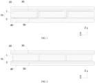
- the photovoltaic module includes first photovoltaic glass 20, a first adhesive film 30, a photovoltaic cell string 10, a second adhesive film 40, and a back support structure 50.
- the first adhesive film 30 and the second adhesive film 40 are oppositely arranged on two sides of the photovoltaic cell string 10, and the first adhesive film 30 is located on a side of the photovoltaic cell string 10 facing sunlight.
- the first photovoltaic glass 20 is arranged on a side of the first adhesive film 30 away from the photovoltaic cell string 10, and the back support structure 50 is arranged on a side of the second adhesive film 40 away from the photovoltaic cell string 10.
- the photovoltaic cell string 10 includes photovoltaic cells 1, and adjacent photovoltaic cells 1 are electrically connected through an electrode line 2 to improve operation efficiency and operation performance of the photovoltaic module.
- the back support structure 50 may be a back sheet. That is, the back support structure 50 is made of an opaque material to enhance structural strength of a side of the photovoltaic module facing away from the sunlight and facilitate mounting of the photovoltaic module, thereby simplifying a mounting structure of the photovoltaic module and shortening a mounting cycle of the photovoltaic module.
- the photovoltaic module is a single glass module.
- the back support structure 50 is second photovoltaic glass. That is, the back support structure 50 is made of a light-transmitting material, so that the side of the photovoltaic module facing away from the sunlight can absorb part of the light, thereby improving utilization of the sunlight by the photovoltaic module and improving photoelectric conversion efficiency of the photovoltaic module.
- the photovoltaic module is a double glass module.
- a specific material and a type of the back support structure 50 and a type of the photovoltaic module are not limited in the embodiments of the present disclosure.
- a diameter d of the electrode line 2 satisfies 0.1 mm ⁇ d ⁇ 0.5 mm.
- the diameter of the electrode line 2 may be 0.1 mm, 0.2 mm, 0.35 mm, 0.46 mm, 0.5 mm, or the like, so as to facilitate machining of the electrode line 2 and reduce a material cost and a machining cost of the electrode line 2.
- 0.1 mm ⁇ d ⁇ 0.5 mm which increases flexibility of a size of the electrode line 2, thereby improving replaceability of the electrode line 2, so as to facilitate subsequent maintenance and replacement of the electrode line 2 and reduce a maintenance cost of the photovoltaic module.
- a thickness of the photovoltaic cell 1 is less than or equal to 140 ⁇ m.
- the thickness of the photovoltaic cell 1 may be 100 ⁇ m, 115 ⁇ m, 126 ⁇ m, 132 ⁇ m, 140 ⁇ m, or the like, so as to facilitate machining of the photovoltaic cell 1 and reduce a material cost and a machining cost of the photovoltaic cell 1.
- a side of the photovoltaic cell 1 facing the sunlight is a front surface of the photovoltaic cell 1, and a side of the photovoltaic cell 1 facing away from the sunlight is a back surface of the photovoltaic cell 1.
- the electrode line 2 has one end located on the back surface of the photovoltaic cell 1 and the other end bending and extending along a thickness direction of the photovoltaic cell 1, and is connected to front surfaces of adjacent photovoltaic cells 1, so as to improve stability of connection between the electrode line and the adjacent photovoltaic cells 1.
- the electrode line 2 is located on the back surface of the photovoltaic cell 1.
- the photovoltaic cell 1 is a back contact cell
- the electrode line 2 is located on the back surface of the photovoltaic cell 1, which reduces shielding of the front surface of the photovoltaic cell 1 by the electrode line 2, thereby increasing a sunlight receiving area of the front surface of the photovoltaic cell 1 and then improving photoelectric conversion efficiency of the photovoltaic cell 1.
- the photovoltaic cell string 10 has a structure as shown in FIG. 1 , that is, when the electrode line 2 has one end soldered and fixed to the back surface of the photovoltaic cell 1 and the other end fixed to the front surface of the adjacent photovoltaic cell 1, after the photovoltaic cell string 10 has been soldered and is cooled to room temperature, the electrode line 2 shrinks under thermal expansion and cold contraction. Since the front surface and the back surface of the photovoltaic cell 1 are fixedly connected to the electrode line 2, shrinkage of the electrode line 2 has little effect on warping of the photovoltaic cell 1.
- the photovoltaic cell 1 is the back contact cell, that is, only the back surface of the photovoltaic cell 1 is fixedly connected to the electrode line 2, after the photovoltaic cell string 10 has been soldered and is cooled to room temperature, the electrode line 2 shrinks under thermal expansion and cold contraction, and the photovoltaic cell 1 may warp towards a direction of the electrode line 2 under the pulling of the electrode line 2, so there is a risk of damage to the photovoltaic cell 1.
- the photovoltaic cell 1 includes a semiconductor substrate 13, a passivation layer 14, busbars 11, and electrode pads 12.
- the electrode line 2 is electrically connected to the electrode pad 12.
- the passivation layer 14 is arranged on a surface of the semiconductor substrate 13.
- the busbar 11 is arranged on a surface of the passivation layer 14.
- the busbar 11 extends along a first direction X, and busbars 11 are spaced apart along a second direction Y. In the first direction X and the second direction Y, one is a length direction of the photovoltaic cell 1, and the other is a width direction of the photovoltaic cell 1.
- the electrode pad 12 is arranged on a side of the busbar 11 away from the passivation layer 14. That is, during manufacturing of the photovoltaic cell 1, the busbar 11 is manufactured on the passivation layer 14 first, and then the electrode pad 12 is manufactured on the busbar 11. A vertical distance between a highest point of the electrode pad 12 and the surface of the passivation layer 14 is L1, and a vertical distance between the busbar 11 and the surface of the passivation layer 14 is L2. L1>L2.
- the electrode line 2 When the electrode line 2 is placed on the electrode pad 12, in the thickness direction Z of the photovoltaic cell 1, there is a gap between the electrode line 2 and the busbar 11, so that a connecting region 21 for connection with the electrode pad 12 and a suspending region 22 in a suspended state located above the gap are formed on the electrode line 2.
- the electrode line 2 When the electrode line 2 is placed on the electrode pad 12 and the electrode line 2 is not soldered and fixed to the photovoltaic cell 1, at least part of the suspending region 22 can bend into the gap, thereby increasing a deformation margin of the electrode line 2.
- part of the suspending region 22 naturally bent on the electrode line 2 is straightened under thermal expansion and cold contraction, thereby reducing risks of deformation of the electrode pad 12 and warping of the semiconductor substrate 13 caused by shrinkage of the electrode line 2 and reducing a risk of deformation of and damage to the photovoltaic cell 1 after soldering and cooling.
- the electrode pad 12 is arranged on the passivation layer 14, the busbar 11 includes connection lines 111 spaced apart along the first direction X, and adjacent connection lines 111 are electrically connected through the electrode pads 12. That is, the electrode pads 12 and the busbars 11 are simultaneously manufactured during the manufacturing of the photovoltaic cell 1. L1 ⁇ L2.
- the electrode line 2 When the electrode line 2 is placed on the electrode pad 12, in the thickness direction Z of the photovoltaic cell 1, and/or in the first direction X, and/or in the second direction Y, there is a gap between the electrode line 2 and the busbar 11, so as to reduce risks of deformation of the electrode pad 12 and warping of the semiconductor substrate 13 caused by shrinkage of the electrode line 2, thereby reducing a risk of deformation of and damage to the photovoltaic cell 1 after soldering and cooling.
- FIG. 5 to FIG. 12 A specific structure of the busbar 11 is shown in FIG. 5 to FIG. 12 .
- the busbar 11 along the thickness direction Z of the photovoltaic cell 1, when L1>L2, as shown in FIG. 5 and FIG. 6 , the busbar 11 has a cuboid structure extending along the first direction X. That is, along the first direction X, the thickness of the busbar 11 is consistent, so as to simplify the structure of the busbar 11 and reduce the manufacturing cost of the busbar 11.
- the electrode line 2 is placed on the electrode pad 12, there is a gap between the electrode line 2 and the busbar 11 in the thickness direction Z of the photovoltaic cell 1.
- the structure of the busbar 11 is shown in FIG. 7 and FIG. 9 .
- part of the busbar 11 is bent towards a direction close to the semiconductor substrate 13 to form a first bending portion 112, so that there is a gap between the electrode line 2 and the busbar 11 in the thickness direction Z of the photovoltaic cell 1.
- part of the busbar 11 can support the electrode line 2, which increases an expansion/contraction margin of the electrode line 2, also increases stability of a connection structure between the electrode line 2 and the photovoltaic cell 1, and reduces a risk of damage due to a small contact area between the electrode line 2 and the electrode pad 12.
- the busbar 11 is provided with the first bending portion 112, which can increase thicknesses of the busbar 11 and the electrode line 2 and also increase a distance between the electrode line 2 and the busbar 11, thereby reducing risks of short service life and poor operation efficiency of the photovoltaic cell 1 caused by a thin busbar 11 and improving operation stability of the photovoltaic cell 1.
- a projection of the first bending portion 112 in the second direction Y is in a shape of U, V, or S or has other deformed structures.
- the specific shape of the first bending portion 112 is not limited in the present disclosure.
- the semiconductor substrate 13 is provided with a groove 131, and at least part of the first bending portion 112 is located in the groove 131.
- part of the passivation layer 14 is located in the groove 131, so that the passivation layer 14 has a pit recessed along the thickness direction Z of the photovoltaic cell 1, and at least part of the first bending portion 112 is located in the pit, which reduces risks of local protrusion of the busbar 11 and abutment against the electrode line 2 caused by interference of the first bending portion 112 with the passivation layer 14, thereby improving flatness of the busbar 11 on the surface of the passivation layer 14 and improving accuracy and stability of a distance between the first bending portion 112 and the electrode line 2.
- the structure of the busbar 11 is shown in FIG. 8 and FIG. 10 .
- part of the busbar 11 is bent towards the direction close to the semiconductor substrate 13 to form a recessed portion 114. That is, along the first direction X, the thickness of the busbar 11 is inconsistent, and the thickness of the busbar 11 decreases at the recessed portion 114. As a result, there is a gap between the electrode line 2 and the busbar 11 in the thickness direction Z of the photovoltaic cell 1.
- the busbar 11 is provided with the recessed portion 114, which meets a requirement for the gap between the electrode line 2 and the busbar 11 and also simplifies structures of the busbar 11 and the semiconductor substrate 13, thereby simplifying manufacturing processes of the semiconductor substrate 13, the passivation layer 14, and the busbar 11, reducing manufacturing costs of the semiconductor substrate 13, the passivation layer 14, and the busbar 11, and shortening manufacturing cycles of the semiconductor substrate 13, the passivation layer 14, and the busbar 11.
- the busbar 11 is provided with the recessed portion 114, which can reduce a height of the electrode pad 12, thereby reducing machining difficulty and a machining cost, i.e., a material cost, of the electrode pad 12.
- a contour of a section of the recessed portion 114 in the thickness direction Z of the photovoltaic cell 1 is in a shape of an arc, U, or V or has other deformed structures.
- the specific shape of the recessed portion 114 is not limited in the present disclosure.
- the structure of the busbar 11 is shown in FIG. 11 and FIG. 12 .
- part of the busbar 11 is bent towards a direction away from the electrode pad 12 to form a second bending portion 113. That is, in a plane defined by the first direction X and the second direction Y, part of the busbar 11 is bent and deformed towards two sides of the electrode line 2 to form the second bending portion 113.
- the second bending portion 113 is located on one side or two sides of the suspending region 22 in the second direction Y
- the busbar 11 is provided with the second bending portion 113 bent in the plane defined by the first direction X and the second direction Y, so that L1 may be equal to L2, thereby simplifying machining procedures of the electrode pad 12 and the busbar 11 and reducing machining difficulty and a machining cost of the busbar 11.
- One or more second bending portions 113 may be provided.
- second bending portions 113 are distributed along the first direction X, and bent directions of adjacent second bending portions 113 are opposite.
- a projection of the second bending portion 113 in the thickness direction Z of the photovoltaic cell 1 is in a shape of U, V, or S or has other deformed structures.
- the specific number and the specific shape of the second bending portion 113 are not limited in the embodiments of the present disclosure.
- the thickness of the busbar 11 is consistent, that is, a projection of the busbar 11 in the second direction Y is in a shape of a rectangle, so as to simplify the structure of the busbar 11 and further reduce the machining cost of the busbar 11.
- the structure of the busbar 11 may be one structure in any one of the above embodiments, or two or more in the above embodiments may be combined to increase diversity and flexibility of the structure of the busbar 11.
- L1 and L2 satisfy 0 ⁇ L1-L2 ⁇ 0.5 mm.
- a difference between L1 and L2 may be 0 mm, 0.1 mm, 0.2 mm, 0.35 mm, 0.4 mm, 0.5 mm, or the like.
- the height of the electrode pad 12 is larger, which increases machining difficulty of the electrode pad 12 and increases machining materials of the electrode pad 12, thereby increasing the machining cost and the material cost of the electrode pad 12. Therefore, if 0 ⁇ L1-L2 ⁇ 0.5 mm, the machining difficulty and the machining cost of the electrode pad 12 are reduced while there is a gap between the electrode line 2 and the busbar 11.
- the busbar 11 may further have the first bending portion 112 as shown in FIG. 7 , to increase a distance between the busbar 11 and the electrode line 2 and also reduce the height of the electrode pad 12. Additionally/alternatively, the busbar 11 may further have the recessed portion 114 as shown in FIG. 8 , to increase the distance between the busbar 11 and the electrode line 2 and also reduce the height of the electrode pad 12. Additionally/alternatively, the busbar 11 may further have the second bending portion 113 as shown in FIG. 12 , so that there is a gap between the busbar 11 and the electrode line in the first direction X and/or the second direction Y, thereby further increasing a size of the suspending region 22 of the electrode line 2.
- the busbar 11 has a same thickness in the thickness direction Z of the photovoltaic cell 1 along the first direction X.
- the busbar has one or more of the first bending portion 112 as shown in FIG. 7 , the recessed portion 114 as shown in FIG. 8 , and the second bending portion 113 as shown in FIG. 12 .
- busbars 11 and electrode pads 12 have a same structure, so as to facilitate machining of the busbars 11 and the electrode pads 12, thereby shortening machining cycles of the busbars 11 and the electrode pads 12 and reducing machining costs of the busbars 11 and the electrode pads 12.
- busbars 11 distributed along the second direction Y and the electrode pads 12 have different structures. That is, during actual machining and manufacturing, one part of the busbars 11 and the electrode pads 12 are machined according to the related art. That is, the busbars 11 and the electrode pads 12 are simultaneously manufactured, and after the electrode lines 2 are fixedly connected to the electrode pad 12, there are no gaps between the electrode line 2 and the part of the busbars 11. At the same time, structures of the other part of the busbars 11 and the electrode pads 12 are a combination of one or more structures in any one of the above embodiments, so that there are gaps between the electrode lines 2 and the part of the busbars 11.
Landscapes
- Photovoltaic Devices (AREA)
- Health & Medical Sciences (AREA)
- Life Sciences & Earth Sciences (AREA)
- Molecular Biology (AREA)
- Sustainable Development (AREA)
Abstract
The present disclosure relates to a photovoltaic cell and a photovoltaic module. The photovoltaic cell includes a semiconductor substrate, a passivation layer arranged on surface of the semiconductor substrate, busbars and electrode pads arranged on the passivation layer. Each of the electrode pads is configured to be electrically connected to electrode line, and along a thickness direction of the photovoltaic cell, the electrode pad is arranged on a side of the busbar away from the passivation layer, or arranged on the passivation layer, the busbar includes connection lines spaced apart along first direction, and adjacent connection lines are electrically connected through electrode pad. Along thickness direction of the photovoltaic cell, vertical distance between a highest point of electrode pad and surface of the passivation layer is L1, and vertical distance between the busbar and the surface of the passivation layer is L2, where L1 and L2 satisfy L1≥L2.
Description
- The present application claims priority to
Chinese Patent Application No. 202310173021.2, filed on February 14, 2023 - The present disclosure relates to the technical field of photovoltaic power generation, and in particular, to a photovoltaic cell and a photovoltaic module.
- A photovoltaic module includes photovoltaic cells and electrode lines, and adjacent photovoltaic cells are electrically connected through the electrode lines to realize series and parallel connection between photovoltaic cells. Each of the photovoltaic cells includes a semiconductor substrate, a passivation layer, and busbars and electrode pads applied to a surface of the passivation layer, electrode pads are arranged at intervals along an extension direction of each of the busbars, and divide the busbar into connection lines. The electrode line is fixedly connected to the electrode pad, and the electrode line covers the busbar, to collect currents on the photovoltaic cells.
- The present disclosure provides a photovoltaic cell and a photovoltaic module, which reduce risks of deformation of and damage to the photovoltaic cell after soldering and cooling.
- In a first aspect of the present application, a photovoltaic cell is provided, including:
- a semiconductor substrate;
- a passivation layer arranged on a surface of the semiconductor substrate;
- busbars arranged on the passivation layer, the busbars extending along a first direction, busbars being spaced apart along a second direction, and in the first direction and the second direction, one being a length direction of the photovoltaic cell, and the other being a width direction of the photovoltaic cell; and
- electrode pads configured to be electrically connected to an electrode line, and arranged on a side of the busbars facing away from the passivation layer along a thickness direction of the photovoltaic cell, or arranged on the passivation layer, one of the busbars including connection lines spaced apart along the first direction, and adjacent connection lines being electrically connected through the electrode pad;
- along the thickness direction of the photovoltaic cell, a vertical distance between a highest point of the electrode pad and a surface of the passivation layer is L1, and a vertical distance between the busbars and the surface of the passivation layer is L2, where L1 and L2 satisfy L1≥L2.
- In the present disclosure, L1≥L2. When the electrode line is placed on the electrode pad, in the thickness direction of the photovoltaic cell, and/or in the first direction, and/or in the second direction, there is a gap between the electrode line and the busbar. After the electrode line and the electrode pad are soldered and fixed and is cooled to room temperature, a naturally bending portion of the electrode line is straightened under thermal expansion and cold contraction, thereby reducing risks of deformation of the electrode pad and warping of the semiconductor substrate caused by shrinkage of the electrode line and reducing risks of deformation of and damage to the photovoltaic cell after soldering and cooling.
- In some embodiments, L1 and L2 satisfy 0≤L1-L2≤0.5 mm.
- In some embodiments, along the thickness direction of the photovoltaic cell, when L1>L2, the busbars have a cuboid structure extending along the first direction.
- In some embodiments, along the thickness direction of the photovoltaic cell, part of the busbar is bent towards a direction close to the semiconductor substrate to form a first bending portion; and
a projection of the first bending portion in the second direction is in a shape of U, V, or S. - In some embodiments, the semiconductor substrate is provided with a groove, and at least part of the first bending portion is located in the groove.
- In some embodiments, along the second direction, a portion of one of the busbars is bent towards a direction away from the electrode pad to form a second bending portion; and
- a projection of the second bending portion in the thickness direction of the photovoltaic cell is in a shape of U, V, or S.
- In some embodiments, a projection of one of the busbars in the second direction is in a shape of a rectangle.
- In some embodiments, along the thickness direction of the photovoltaic cell, a portion of one of the busbars is bent towards a direction close to the semiconductor substrate to form a recessed portion; and
a contour of a section of the recessed portion in the thickness direction of the photovoltaic cell is in a shape of an arc, U, or V. - In a second aspect of the present disclosure, a photovoltaic module is provided, including:
- photovoltaic cells, adjacent photovoltaic cells being electrically connected through an electrode line, one of the photovoltaic cells including a first surface and a second surface arranged oppositely along an own thickness direction, the first surface being located on a side facing sunlight;
- first photovoltaic glass arranged on the first surface, a first adhesive film being arranged between the first photovoltaic glass and the first surface; and
- a back support structure arranged on the second surface, a second adhesive film being arranged between the back support structure and the second surface;
- the back support structure being a back sheet or second photovoltaic glass;
- wherein the photovoltaic cell includes a semiconductor substrate, a passivation layer, busbars, and electrode pads, and the electrode line is electrically connected to the electrode pads;
- the passivation layer is arranged on a surface of the semiconductor substrate;
- each of the busbars is arranged on the passivation layer, the busbar extends along a first direction, busbars are spaced apart along a second direction, and in the first direction and the second direction, one is a length direction of the photovoltaic cell, and the other is a width direction of the photovoltaic cell;
- along a thickness direction of the photovoltaic cell, the electrode pad is arranged on a side of the busbar away from the passivation layer, or each of the electrode pads is arranged on the passivation layer, the busbar includes connection lines spaced apart along the first direction, and adjacent connection lines are electrically connected through the electrode pad; and
- along the thickness direction of the photovoltaic cell, a vertical distance between a highest point of the electrode pad and a surface of the passivation layer is L1, and a vertical distance between the busbars and the surface of the passivation layer is L2, where L1 and L2 satisfy L1≥L2.
- In the present disclosure, there is a gap between the electrode line and the busbar, which increases a deformation margin of the electrode line, and reduces risks of deformation of the electrode pad and warping of the semiconductor substrate caused by shrinkage of the electrode line. During machining, assembly, and use of the photovoltaic module, risks of shrinkage of and damage to the electrode line and deformation of the photovoltaic cell caused by changes in ambient temperature and changes in a temperature of the photovoltaic module are reduced, thereby improving operation stability of the photovoltaic module and prolonging the service life of the photovoltaic module.
- In some embodiments, a diameter d of the electrode line satisfies 0.1 mm≤d≤0.5 mm.
- It should be understood that the general description above and the detailed description in the following are merely exemplary and illustrative, and cannot limit the present disclosure.
-
-
FIG. 1 is a sectional view of a photovoltaic module according to the present disclosure in some embodiments; -
FIG. 2 is a sectional view of the photovoltaic module according to the present disclosure in some other embodiments; -
FIG. 3 is a schematic diagram of a surface structure of a photovoltaic cell according to the present disclosure in some embodiments; -
FIG. 4 is a schematic diagram of a partial structure of the photovoltaic cell inFIG. 3 connected to an electrode line in some embodiments, where the electrode line is in a shrunk state; -
FIG. 5 is a schematic diagram of a partial structure of the photovoltaic cell inFIG. 3 connected to the electrode line in some other embodiments, where the electrode line is in an unshrunk state; -
FIG. 6 is a schematic structural diagram of the electrode line inFIG. 5 after shrinkage; -
FIG. 7 is a schematic diagram of a partial structure of the photovoltaic cell inFIG. 3 connected to the electrode line in some other embodiments, where the electrode line is in a shrunk state; -
FIG. 8 is a schematic diagram of a partial structure of the photovoltaic cell inFIG. 3 connected to the electrode line in some other embodiments, where the electrode line is in a shrunk state; -
FIG. 9 is a schematic diagram of a partial structure of the photovoltaic cell inFIG. 3 connected to the electrode line in some other embodiments, where the electrode line is in a shrunk state; -
FIG. 10 is a schematic diagram of a partial structure of the photovoltaic cell inFIG. 3 connected to the electrode line in some other embodiments, where the electrode line is in a shrunk state; -
FIG. 11 is a schematic structure diagram of the photovoltaic cell according to the present disclosure connected to the electrode line in some other embodiments; and -
FIG. 12 is a schematic diagram of a surface structure of the photovoltaic cell inFIG. 11 . - Reference signs:
- 1: photovoltaic cell;
- 11: busbar;
- 111: connection line;
- 112: first bending portion;
- 113: second bending portion;
- 114: recessed portion;
- 12: electrode pad;
- 13: semiconductor substrate;
13 1: groove; - 14: passivation layer;
- 11: busbar;
- 2: electrode line;
- 21: connecting region;
- 22: suspending region;
- 10: photovoltaic cell string;
- 20: first photovoltaic glass;
- 30: first adhesive film;
- 40: second adhesive film;
- 50: back support structure.
- The accompanying drawings herein, which are incorporated in and constitute a part of this specification, illustrate embodiments consistent with the present disclosure and, together with the specification, serve to explain principles of the present disclosure.
- In order to better understand the technical solutions of the present disclosure, embodiments of the present disclosure will be described in detail below in conjunction with the accompanying drawings.
- It should be clear that the described embodiments are only some rather than all of the embodiments of the present disclosure. Based on the embodiments in the present disclosure, all other embodiments obtained by those of ordinary skill in the art without creative efforts fall within the protection scope of the present disclosure.
- Terms used in the embodiments of the present disclosure are only for the purpose of describing specific embodiments, and are not intended to limit the present disclosure. Singular forms of "a/an", "the", and "said" used in the embodiments of the present disclosure and the appended claims are intended to include plural forms, unless otherwise clearly specified in the context.
- It should be understood that the term "and/or" used herein describes an association relationship between associated objects and represents that three relationships may exist. For example, A and/or B may represent the following three cases: only A exists, both A and B exist, and only B exists. In addition, the character "/" herein generally indicates an "or" relationship between the associated objects.
- It is to be noted that orientation terms such as "up", "down", "left", and "right" described in the embodiments of the present disclosure are described from the perspective shown in the accompanying drawings, and should not be construed as limiting the embodiments of the present disclosure. Besides, in this context, it is to be further understood that one element described as being connected "on" or "under" another element not only means that the element may be directly connected "on" or "under" the another element, but also means that the element may be indirectly connected "on" or "under" the another element through an intermediate element.
- In the related art, the electrode line is directly attached to the surface of the photovoltaic cell. After the electrode line and the electrode pad are soldered and fixed at a certain soldering temperature, when the electrode line and the photovoltaic cell are cooled to room temperature, due to different thermal expansion coefficients of the electrode line and the photovoltaic cell, shrinkage of the electrode line leads to warping of the photovoltaic cell, increasing a risk of damage to the photovoltaic cell.
- Some embodiments of the present disclosure provide a photovoltaic module. As shown in
FIG. 1 and FIG. 2 , the photovoltaic module includes firstphotovoltaic glass 20, a firstadhesive film 30, aphotovoltaic cell string 10, a secondadhesive film 40, and aback support structure 50. Along a thickness direction of the photovoltaic module, the firstadhesive film 30 and the secondadhesive film 40 are oppositely arranged on two sides of thephotovoltaic cell string 10, and the firstadhesive film 30 is located on a side of thephotovoltaic cell string 10 facing sunlight. The firstphotovoltaic glass 20 is arranged on a side of the firstadhesive film 30 away from thephotovoltaic cell string 10, and theback support structure 50 is arranged on a side of the secondadhesive film 40 away from thephotovoltaic cell string 10. Thephotovoltaic cell string 10 includesphotovoltaic cells 1, and adjacentphotovoltaic cells 1 are electrically connected through anelectrode line 2 to improve operation efficiency and operation performance of the photovoltaic module. - In some embodiments, the
back support structure 50 may be a back sheet. That is, theback support structure 50 is made of an opaque material to enhance structural strength of a side of the photovoltaic module facing away from the sunlight and facilitate mounting of the photovoltaic module, thereby simplifying a mounting structure of the photovoltaic module and shortening a mounting cycle of the photovoltaic module. In this case, the photovoltaic module is a single glass module. - In some other embodiments, the
back support structure 50 is second photovoltaic glass. That is, theback support structure 50 is made of a light-transmitting material, so that the side of the photovoltaic module facing away from the sunlight can absorb part of the light, thereby improving utilization of the sunlight by the photovoltaic module and improving photoelectric conversion efficiency of the photovoltaic module. In this case, the photovoltaic module is a double glass module. A specific material and a type of theback support structure 50 and a type of the photovoltaic module are not limited in the embodiments of the present disclosure. - A diameter d of the
electrode line 2 satisfies 0.1 mm≤d≤0.5 mm. For example, the diameter of theelectrode line 2 may be 0.1 mm, 0.2 mm, 0.35 mm, 0.46 mm, 0.5 mm, or the like, so as to facilitate machining of theelectrode line 2 and reduce a material cost and a machining cost of theelectrode line 2. At the same time, 0.1 mm≤d≤0.5 mm, which increases flexibility of a size of theelectrode line 2, thereby improving replaceability of theelectrode line 2, so as to facilitate subsequent maintenance and replacement of theelectrode line 2 and reduce a maintenance cost of the photovoltaic module. - A thickness of the
photovoltaic cell 1 is less than or equal to 140 µm. For example, the thickness of thephotovoltaic cell 1 may be 100 µm, 115 µm, 126 µm, 132 µm, 140 µm, or the like, so as to facilitate machining of thephotovoltaic cell 1 and reduce a material cost and a machining cost of thephotovoltaic cell 1. - A side of the
photovoltaic cell 1 facing the sunlight is a front surface of thephotovoltaic cell 1, and a side of thephotovoltaic cell 1 facing away from the sunlight is a back surface of thephotovoltaic cell 1. - In some embodiments, as shown in
FIG. 1 , theelectrode line 2 has one end located on the back surface of thephotovoltaic cell 1 and the other end bending and extending along a thickness direction of thephotovoltaic cell 1, and is connected to front surfaces of adjacentphotovoltaic cells 1, so as to improve stability of connection between the electrode line and the adjacentphotovoltaic cells 1. - In some other embodiments, as shown in
FIG. 2 , theelectrode line 2 is located on the back surface of thephotovoltaic cell 1. In this case, thephotovoltaic cell 1 is a back contact cell, and theelectrode line 2 is located on the back surface of thephotovoltaic cell 1, which reduces shielding of the front surface of thephotovoltaic cell 1 by theelectrode line 2, thereby increasing a sunlight receiving area of the front surface of thephotovoltaic cell 1 and then improving photoelectric conversion efficiency of thephotovoltaic cell 1. - When the
photovoltaic cell string 10 has a structure as shown inFIG. 1 , that is, when theelectrode line 2 has one end soldered and fixed to the back surface of thephotovoltaic cell 1 and the other end fixed to the front surface of the adjacentphotovoltaic cell 1, after thephotovoltaic cell string 10 has been soldered and is cooled to room temperature, theelectrode line 2 shrinks under thermal expansion and cold contraction. Since the front surface and the back surface of thephotovoltaic cell 1 are fixedly connected to theelectrode line 2, shrinkage of theelectrode line 2 has little effect on warping of thephotovoltaic cell 1. - When the
photovoltaic cell 1 is the back contact cell, that is, only the back surface of thephotovoltaic cell 1 is fixedly connected to theelectrode line 2, after thephotovoltaic cell string 10 has been soldered and is cooled to room temperature, theelectrode line 2 shrinks under thermal expansion and cold contraction, and thephotovoltaic cell 1 may warp towards a direction of theelectrode line 2 under the pulling of theelectrode line 2, so there is a risk of damage to thephotovoltaic cell 1. - In order to solve the problem of the warping of the back contact cell, in a second aspect, some embodiments of the present disclosure provide a
photovoltaic cell 1. As shown inFIG. 3 to FIG. 12 , thephotovoltaic cell 1 includes asemiconductor substrate 13, apassivation layer 14,busbars 11, andelectrode pads 12. Theelectrode line 2 is electrically connected to theelectrode pad 12. Thepassivation layer 14 is arranged on a surface of thesemiconductor substrate 13. Thebusbar 11 is arranged on a surface of thepassivation layer 14. Thebusbar 11 extends along a first direction X, andbusbars 11 are spaced apart along a second direction Y. In the first direction X and the second direction Y, one is a length direction of thephotovoltaic cell 1, and the other is a width direction of thephotovoltaic cell 1. - In some embodiments, as shown in
FIG. 3 and FIG. 4 , along a thickness direction Z of thephotovoltaic cell 1, theelectrode pad 12 is arranged on a side of thebusbar 11 away from thepassivation layer 14. That is, during manufacturing of thephotovoltaic cell 1, thebusbar 11 is manufactured on thepassivation layer 14 first, and then theelectrode pad 12 is manufactured on thebusbar 11. A vertical distance between a highest point of theelectrode pad 12 and the surface of thepassivation layer 14 is L1, and a vertical distance between thebusbar 11 and the surface of thepassivation layer 14 is L2. L1>L2. - When the
electrode line 2 is placed on theelectrode pad 12, in the thickness direction Z of thephotovoltaic cell 1, there is a gap between theelectrode line 2 and thebusbar 11, so that a connectingregion 21 for connection with theelectrode pad 12 and a suspendingregion 22 in a suspended state located above the gap are formed on theelectrode line 2. When theelectrode line 2 is placed on theelectrode pad 12 and theelectrode line 2 is not soldered and fixed to thephotovoltaic cell 1, at least part of the suspendingregion 22 can bend into the gap, thereby increasing a deformation margin of theelectrode line 2. After theelectrode line 2 is soldered and fixed to theelectrode pad 12 and is cooled to room temperature, part of the suspendingregion 22 naturally bent on theelectrode line 2 is straightened under thermal expansion and cold contraction, thereby reducing risks of deformation of theelectrode pad 12 and warping of thesemiconductor substrate 13 caused by shrinkage of theelectrode line 2 and reducing a risk of deformation of and damage to thephotovoltaic cell 1 after soldering and cooling. At the same time, during machining, assembly, and use of the photovoltaic module, risks of shrinkage of and damage to theelectrode line 2 and deformation of thephotovoltaic cell 1 caused by changes in ambient temperature and changes in a temperature of the photovoltaic module are reduced, thereby improving operation stability of the photovoltaic module and prolonging the service life of the photovoltaic module. - In some other embodiments, as shown in
FIG. 3 ,FIG. 5, and FIG. 6 , theelectrode pad 12 is arranged on thepassivation layer 14, thebusbar 11 includesconnection lines 111 spaced apart along the first direction X, andadjacent connection lines 111 are electrically connected through theelectrode pads 12. That is, theelectrode pads 12 and thebusbars 11 are simultaneously manufactured during the manufacturing of thephotovoltaic cell 1. L1≥L2. When theelectrode line 2 is placed on theelectrode pad 12, in the thickness direction Z of thephotovoltaic cell 1, and/or in the first direction X, and/or in the second direction Y, there is a gap between theelectrode line 2 and thebusbar 11, so as to reduce risks of deformation of theelectrode pad 12 and warping of thesemiconductor substrate 13 caused by shrinkage of theelectrode line 2, thereby reducing a risk of deformation of and damage to thephotovoltaic cell 1 after soldering and cooling. At the same time, risks of shrinkage of and damage to theelectrode line 2 and deformation of thephotovoltaic cell 1 caused by changes in ambient temperature and changes in a temperature of the photovoltaic module are reduced, thereby improving operation stability of the photovoltaic module and prolonging the service life of the photovoltaic module. - A specific structure of the
busbar 11 is shown inFIG. 5 to FIG. 12 . In some embodiments, along the thickness direction Z of thephotovoltaic cell 1, when L1>L2, as shown inFIG. 5 and FIG. 6 , thebusbar 11 has a cuboid structure extending along the first direction X. That is, along the first direction X, the thickness of thebusbar 11 is consistent, so as to simplify the structure of thebusbar 11 and reduce the manufacturing cost of thebusbar 11. In this embodiment, when theelectrode line 2 is placed on theelectrode pad 12, there is a gap between theelectrode line 2 and thebusbar 11 in the thickness direction Z of thephotovoltaic cell 1. - In some other embodiments, the structure of the
busbar 11 is shown inFIG. 7 andFIG. 9 . Along the thickness direction Z of thephotovoltaic cell 1, part of thebusbar 11 is bent towards a direction close to thesemiconductor substrate 13 to form afirst bending portion 112, so that there is a gap between theelectrode line 2 and thebusbar 11 in the thickness direction Z of thephotovoltaic cell 1. - In this embodiment, when L1=L2, as shown in
FIG. 7 , part of thebusbar 11 can support theelectrode line 2, which increases an expansion/contraction margin of theelectrode line 2, also increases stability of a connection structure between theelectrode line 2 and thephotovoltaic cell 1, and reduces a risk of damage due to a small contact area between theelectrode line 2 and theelectrode pad 12. When L1>L2, as shown inFIG. 9 , thebusbar 11 is provided with thefirst bending portion 112, which can increase thicknesses of thebusbar 11 and theelectrode line 2 and also increase a distance between theelectrode line 2 and thebusbar 11, thereby reducing risks of short service life and poor operation efficiency of thephotovoltaic cell 1 caused by athin busbar 11 and improving operation stability of thephotovoltaic cell 1. - Furthermore a projection of the
first bending portion 112 in the second direction Y is in a shape of U, V, or S or has other deformed structures. The specific shape of thefirst bending portion 112 is not limited in the present disclosure. - For example, as shown in
FIG. 7 andFIG. 9 , thesemiconductor substrate 13 is provided with agroove 131, and at least part of thefirst bending portion 112 is located in thegroove 131. - In this embodiment, part of the
passivation layer 14 is located in thegroove 131, so that thepassivation layer 14 has a pit recessed along the thickness direction Z of thephotovoltaic cell 1, and at least part of thefirst bending portion 112 is located in the pit, which reduces risks of local protrusion of thebusbar 11 and abutment against theelectrode line 2 caused by interference of thefirst bending portion 112 with thepassivation layer 14, thereby improving flatness of thebusbar 11 on the surface of thepassivation layer 14 and improving accuracy and stability of a distance between thefirst bending portion 112 and theelectrode line 2. - In some other embodiments, the structure of the
busbar 11 is shown inFIG. 8 andFIG. 10 . Along the thickness direction Z of thephotovoltaic cell 1, part of thebusbar 11 is bent towards the direction close to thesemiconductor substrate 13 to form a recessedportion 114. That is, along the first direction X, the thickness of thebusbar 11 is inconsistent, and the thickness of thebusbar 11 decreases at the recessedportion 114. As a result, there is a gap between theelectrode line 2 and thebusbar 11 in the thickness direction Z of thephotovoltaic cell 1. - In this embodiment, the
busbar 11 is provided with the recessedportion 114, which meets a requirement for the gap between theelectrode line 2 and thebusbar 11 and also simplifies structures of thebusbar 11 and thesemiconductor substrate 13, thereby simplifying manufacturing processes of thesemiconductor substrate 13, thepassivation layer 14, and thebusbar 11, reducing manufacturing costs of thesemiconductor substrate 13, thepassivation layer 14, and thebusbar 11, and shortening manufacturing cycles of thesemiconductor substrate 13, thepassivation layer 14, and thebusbar 11. At the same time, thebusbar 11 is provided with the recessedportion 114, which can reduce a height of theelectrode pad 12, thereby reducing machining difficulty and a machining cost, i.e., a material cost, of theelectrode pad 12. At the same time, structural stability of theelectrode pad 12 is improved, and a risk of damage to theelectrode pad 12 due to an external force during machining, mounting, transportation, and use is reduced, thereby prolonging the service life of theelectrode pad 12, prolonging the service life of thephotovoltaic cell 1 and the photovoltaic module, and improving operation stability of thephotovoltaic cell 1 and the photovoltaic module. - Furthermore, a contour of a section of the recessed
portion 114 in the thickness direction Z of thephotovoltaic cell 1 is in a shape of an arc, U, or V or has other deformed structures. The specific shape of the recessedportion 114 is not limited in the present disclosure. - In some other embodiments, the structure of the
busbar 11 is shown inFIG. 11 and FIG. 12 . Along the second direction Y, part of thebusbar 11 is bent towards a direction away from theelectrode pad 12 to form asecond bending portion 113. That is, in a plane defined by the first direction X and the second direction Y, part of thebusbar 11 is bent and deformed towards two sides of theelectrode line 2 to form thesecond bending portion 113. As a result, there is a gap between theelectrode line 2 and thebusbar 11 in the first direction X and/or the second direction Y. In this case, thesecond bending portion 113 is located on one side or two sides of the suspendingregion 22 in the second direction Y - In this embodiment, the
busbar 11 is provided with thesecond bending portion 113 bent in the plane defined by the first direction X and the second direction Y, so that L1 may be equal to L2, thereby simplifying machining procedures of theelectrode pad 12 and thebusbar 11 and reducing machining difficulty and a machining cost of thebusbar 11. - Furthermore, One or more
second bending portions 113 may be provided.second bending portions 113 are distributed along the first direction X, and bent directions of adjacentsecond bending portions 113 are opposite. A projection of thesecond bending portion 113 in the thickness direction Z of thephotovoltaic cell 1 is in a shape of U, V, or S or has other deformed structures. The specific number and the specific shape of thesecond bending portion 113 are not limited in the embodiments of the present disclosure. - In addition, along the first direction X, the thickness of the
busbar 11 is consistent, that is, a projection of thebusbar 11 in the second direction Y is in a shape of a rectangle, so as to simplify the structure of thebusbar 11 and further reduce the machining cost of thebusbar 11. - During the manufacturing of the
busbar 11, the structure of thebusbar 11 may be one structure in any one of the above embodiments, or two or more in the above embodiments may be combined to increase diversity and flexibility of the structure of thebusbar 11. - In any one of the above embodiments, L1 and L2 satisfy 0≤L1-L2≤0.5 mm. For example, a difference between L1 and L2 may be 0 mm, 0.1 mm, 0.2 mm, 0.35 mm, 0.4 mm, 0.5 mm, or the like.
- In this embodiment, if L1-L2>0.5 mm, the height of the
electrode pad 12 is larger, which increases machining difficulty of theelectrode pad 12 and increases machining materials of theelectrode pad 12, thereby increasing the machining cost and the material cost of theelectrode pad 12. Therefore, if 0≤L1-L2≤0.5 mm, the machining difficulty and the machining cost of theelectrode pad 12 are reduced while there is a gap between theelectrode line 2 and thebusbar 11. - To sum up, as shown in
FIG. 4 , when theelectrode pad 12 is arranged on thebusbar 11, L1>L2. In this case, thebusbar 11 may further have thefirst bending portion 112 as shown inFIG. 7 , to increase a distance between thebusbar 11 and theelectrode line 2 and also reduce the height of theelectrode pad 12. Additionally/alternatively, thebusbar 11 may further have the recessedportion 114 as shown inFIG. 8 , to increase the distance between thebusbar 11 and theelectrode line 2 and also reduce the height of theelectrode pad 12. Additionally/alternatively, thebusbar 11 may further have thesecond bending portion 113 as shown inFIG. 12 , so that there is a gap between thebusbar 11 and the electrode line in the first direction X and/or the second direction Y, thereby further increasing a size of the suspendingregion 22 of theelectrode line 2. - When the
electrode pad 12 is placed on thepassivation layer 14 and theelectrode pad 12 divides thebusbar 11 intoconnection lines 111 as shown inFIG. 6 and when L1=L2, thebusbar 11 has thefirst bending portion 112 as shown inFIG. 7 , so that there is a gap between thebusbar 11 and theelectrode line 2 in the thickness direction Z of thephotovoltaic cell 1. Additionally/alternatively, thebusbar 11 has the recessedportion 114 as shown inFIG. 8 , so that there is a gap between thebusbar 11 and theelectrode line 2 in the thickness direction Z of thephotovoltaic cell 1. Additionally/alternatively, thebusbar 11 has thesecond bending portion 113 as shown inFIG. 12 , so that there is a gap between thebusbar 11 and theelectrode line 2 in the first direction X and/or the second direction Y - As shown in
FIG. 6 , when theelectrode pad 12 is placed on thepassivation layer 14 and theelectrode pad 12 divides thebusbar 11 intoconnection lines 111 and when L1>L2, thebusbar 11 has a same thickness in the thickness direction Z of thephotovoltaic cell 1 along the first direction X. Alternatively, the busbar has one or more of thefirst bending portion 112 as shown inFIG. 7 , the recessedportion 114 as shown inFIG. 8 , and thesecond bending portion 113 as shown inFIG. 12 . - In addition, in some embodiments,
busbars 11 andelectrode pads 12 have a same structure, so as to facilitate machining of thebusbars 11 and theelectrode pads 12, thereby shortening machining cycles of thebusbars 11 and theelectrode pads 12 and reducing machining costs of thebusbars 11 and theelectrode pads 12. - In some other embodiments,
busbars 11 distributed along the second direction Y and theelectrode pads 12 have different structures. That is, during actual machining and manufacturing, one part of thebusbars 11 and theelectrode pads 12 are machined according to the related art. That is, thebusbars 11 and theelectrode pads 12 are simultaneously manufactured, and after theelectrode lines 2 are fixedly connected to theelectrode pad 12, there are no gaps between theelectrode line 2 and the part of thebusbars 11. At the same time, structures of the other part of thebusbars 11 and theelectrode pads 12 are a combination of one or more structures in any one of the above embodiments, so that there are gaps between theelectrode lines 2 and the part of thebusbars 11. - In this embodiment, there is a gap between the
electrode line 2 and part of thebusbar 11, which reduces a total machining cost of thebusbar 11 and reduces an influence of shrinkage of theelectrode line 2 on the warping of thephotovoltaic cell 1, thereby prolonging the service life and improve operation stability of the photovoltaic cell. - The above descriptions are only preferred embodiments of the present disclosure, and are not intended to limit the present disclosure. For those skilled in the art, various modifications and changes may be made to the present disclosure. Any modifications, equivalent replacements, improvements, and the like made within the spirit and the principle of the present disclosure shall fall within the protection scope of the present disclosure.
Claims (15)
- A photovoltaic cell (1), comprising:a semiconductor substrate (13);a passivation layer (14) arranged on a surface of the semiconductor substrate (13);busbars (11) arranged on the passivation layer (14), wherein the busbars (11) extend along a first direction (X), and are spaced apart from one another along a second direction (Y), wherein one of the first direction (X) and the second direction (Y) is a length direction of the photovoltaic cell (1), and the other of the first direction (X) and the second direction (Y) is a width direction of the photovoltaic cell (1); andelectrode pads (12) configured to be electrically connected to an electrode line (2), wherein the electrode pads (12) are arranged on a side of the busbars (11) facing away from the passivation layer (14) along a thickness direction (Z) of the photovoltaic cell (1), or are arranged on the passivation layer (14) along a thickness direction (Z) of the photovoltaic cell (1), wherein, one of the busbars (11) comprises connection lines (111) spaced apart from each other along the first direction (X), and adjacent connection lines (111) are electrically connected through corresponding electrode pad (12);wherein, along the thickness direction (Z) of the photovoltaic cell (1), a vertical distance between a highest point of the electrode pad (12) and a surface of the passivation layer (14) is L1, and a vertical distance between the busbars (11) and the surface of the passivation layer (14) is L2, where L1 and L2 satisfy L1≥L2.
- The photovoltaic cell according to claim 1, wherein L1 and L2 satisfy 0≤L1-L2≤0.5 mm.
- The photovoltaic cell according to claim 2, wherein L1 and L2 satisfy 0.1≤L1-L2≤0.4 mm.
- The photovoltaic cell according to claim 1, wherein, when L1>L2, the busbars (11) have a cuboid structure extending along the first direction (X) along the thickness direction (Z) of the photovoltaic cell (1).
- The photovoltaic cell according to claim 1, wherein, part of the busbars (11) is bent towards a direction close to the semiconductor substrate (13) to form a first bending portion (112) along the thickness direction (Z) of the photovoltaic cell (1); and
a projection of the first bending portion (112) in the second direction (Y) is in a shape of U, V, or S. - The photovoltaic cell according to claim 5, wherein the semiconductor substrate (13) is provided with a groove (131), and at least part of the first bending portion (112) is located in the groove (131).
- The photovoltaic cell according to claim 1, wherein, a portion of one of the busbars (11) is bent towards a direction facing away from the electrode pad (12) to form a second bending portion (113) along the second direction (Y); and
a projection of the second bending portion (113) in the thickness direction (Z) of the photovoltaic cell (1) is in a shape of U, V, or S. - The photovoltaic cell according to claim 7, wherein a projection of one of the busbars (11) in the second direction (Y) is in a shape of a rectangle.
- The photovoltaic cell according to claim 1, wherein, along the thickness direction (Z) of the photovoltaic cell (1), a portion of one of the busbars (11) is bent towards a direction close to the semiconductor substrate (13) to form a recessed portion (114); and
a contour of a section of the recessed portion (114) in the thickness direction (Z) of the photovoltaic cell (1) is in a shape of an arc, U, or V. - The photovoltaic cell according to claim 7, wherein, along the thickness direction (Z) of the photovoltaic cell (1), a portion of one of the busbars (11) is bent towards a direction close to the semiconductor substrate (13) to form a recessed portion (114); and
a contour of a section of the recessed portion (114) in the thickness direction (Z) of the photovoltaic cell (1) is in a shape of an arc, U, or V. - A photovoltaic module, comprising:photovoltaic cells (1), wherein, adjacent photovoltaic cells (1) are electrically connected through a corresponding electrode line (2), one of the photovoltaic cells (1) comprises a first surface and a second surface arranged oppositely along an thickness direction (Z) of the photovoltaic cells, and the first surface is located on a side facing sunlight;first photovoltaic glass (20) arranged on the first surface, wherein a first adhesive film (30) is arranged between the first photovoltaic glass (20) and the first surface; anda back support structure (50) arranged on the second surface, wherein a second adhesive film (40) is arranged between the back support structure (50) and the second surface;wherein the back support structure (50) is a back sheet or second photovoltaic glass;wherein the photovoltaic cell (1) comprises a semiconductor substrate (13), a passivation layer (14), busbars (11), and electrode pads (12), and the electrode line (2) is electrically connected to a corresponding electrode pad (12);wherein the passivation layer (14) is arranged on a surface of the semiconductor substrate (13);the busbars (11) are arranged on the passivation layer (14), extends along a first direction (X), and spaced apart from each other along a second direction (Y), and, one of the first direction (X) and the second direction (Y) is a length direction of the photovoltaic cell (1), and the other of the first direction (X) and the second direction (Y) is a width direction of the photovoltaic cell (1);the electrode pad (12) is arranged on a side of the busbars (11) facing away from the passivation layer (14), or is arranged on the passivation layer (14) along a thickness direction (Z) of the photovoltaic cell (1), one of the busbars (11) comprises connection lines (111) spaced apart from one another along the first direction (X), and adjacent connection lines (111) are electrically connected through corresponding electrode pad (12); andalong the thickness direction (Z) of the photovoltaic cell (1), a vertical distance between a highest point of the electrode pad (12) and a surface of the passivation layer (14) is L1, and a vertical distance between the busbars (11) and the surface of the passivation layer (14) is L2, where L1 and L2 satisfy L1≥L2.
- The photovoltaic module according to claim 11, wherein a diameter d of the electrode line (2) satisfies 0.1 mm≤d≤0.5 mm.
- The photovoltaic cell according to claim 11, wherein L1 and L2 satisfy 0≤L1-L2≤0.5 mm.
- The photovoltaic cell according to claim 13, wherein L1 and L2 satisfy 0.1≤L1-L2≤0.4 mm.
- The photovoltaic cell according to claim 11, wherein, when L1>L2, the busbars (11) have a cuboid structure extending along the first direction (X) along the thickness direction (Z) of the photovoltaic cell (1).
Applications Claiming Priority (1)
| Application Number | Priority Date | Filing Date | Title |
|---|---|---|---|
| CN202310173021.2A CN116031314A (en) | 2023-02-14 | 2023-02-14 | Photovoltaic cells and photovoltaic modules |
Publications (1)
| Publication Number | Publication Date |
|---|---|
| EP4418331A1 true EP4418331A1 (en) | 2024-08-21 |
Family
ID=86077715
Family Applications (1)
| Application Number | Title | Priority Date | Filing Date |
|---|---|---|---|
| EP23199616.6A Pending EP4418331A1 (en) | 2023-02-14 | 2023-09-26 | Photovoltaic cell and photovoltaic module |
Country Status (6)
| Country | Link |
|---|---|
| US (1) | US12302647B2 (en) |
| EP (1) | EP4418331A1 (en) |
| JP (1) | JP7488950B1 (en) |
| CN (1) | CN116031314A (en) |
| AU (1) | AU2023237055B2 (en) |
| DE (1) | DE202023107686U1 (en) |
Families Citing this family (3)
| Publication number | Priority date | Publication date | Assignee | Title |
|---|---|---|---|---|
| WO2025060777A1 (en) * | 2023-09-22 | 2025-03-27 | 珠海富山爱旭太阳能科技有限公司 | Solar cell sheet, cell assembly and photovoltaic system |
| CN121194557A (en) * | 2025-11-24 | 2025-12-23 | 浙江晶科能源有限公司 | Photovoltaic cells and photovoltaic modules |
| CN121194567B (en) * | 2025-11-26 | 2026-02-24 | 晶科能源(海宁)有限公司 | Photovoltaic module and method for manufacturing same |
Citations (4)
| Publication number | Priority date | Publication date | Assignee | Title |
|---|---|---|---|---|
| US20120222740A1 (en) * | 2009-03-03 | 2012-09-06 | Jinah Kim | Solar cell and method for manufacturing the same, and solar cell module |
| US20140332072A1 (en) * | 2011-12-13 | 2014-11-13 | Dow Corning Corporation | Photovoltaic Cell And Method Of Forming The Same |
| US20160020349A1 (en) * | 2013-03-28 | 2016-01-21 | Panasonic Intellectual Property Management Co., Ltd. | Solar cell module and solar cell module manufacturing method |
| WO2022143352A1 (en) * | 2020-12-30 | 2022-07-07 | 通威太阳能(成都)有限公司 | Solar cell and front electrode thereof, and manufacturing method |
Family Cites Families (21)
| Publication number | Priority date | Publication date | Assignee | Title |
|---|---|---|---|---|
| JP4040659B2 (en) * | 2006-04-14 | 2008-01-30 | シャープ株式会社 | Solar cell, solar cell string, and solar cell module |
| JP4429306B2 (en) * | 2006-12-25 | 2010-03-10 | 三洋電機株式会社 | Solar cell and solar cell module |
| JP2011187567A (en) * | 2010-03-05 | 2011-09-22 | Sanyo Electric Co Ltd | Solar cell module |
| RU2597573C2 (en) * | 2011-01-31 | 2016-09-10 | Син-Эцу Кемикал Ко., Лтд. | Stencil master for solar cell and method for printing electrode of solar cell |
| KR101239793B1 (en) | 2011-11-29 | 2013-03-06 | 엘지전자 주식회사 | Solar cell and mehtod for manufacturing the same |
| KR102257808B1 (en) | 2014-01-20 | 2021-05-28 | 엘지전자 주식회사 | Solar cell module |
| US11532765B2 (en) * | 2015-04-30 | 2022-12-20 | Shangrao Jinko Solar Technology Development Co., Ltd | Solar cell and solar cell panel including the same |
| FR3037441B1 (en) * | 2015-06-10 | 2017-07-21 | Commissariat Energie Atomique | PHOTOVOLTAIC MODULE AND METHOD FOR INTERCONNECTING PHOTOVOLTAIC CELLS TO MANUFACTURE SUCH A MODULE |
| EP3381047A4 (en) * | 2015-11-24 | 2019-07-03 | Hitachi Chemical Co., Ltd. | COATED MULTILAYER STACKS FOR INTEGRATED CIRCUITS AND SOLAR CELLS |
| JP6501906B2 (en) * | 2015-11-25 | 2019-04-17 | 三井化学東セロ株式会社 | Solar cell module |
| JP6714275B2 (en) | 2016-08-23 | 2020-06-24 | ナミックス株式会社 | Conductive paste and solar cell |
| US11462652B2 (en) | 2016-09-27 | 2022-10-04 | Lg Electronics Inc. | Solar cell and solar cell panel including the same |
| US10937915B2 (en) * | 2016-10-28 | 2021-03-02 | Tesla, Inc. | Obscuring, color matching, and camouflaging solar panels |
| WO2018173125A1 (en) * | 2017-03-21 | 2018-09-27 | 三菱電機株式会社 | Solar cell and solar module |
| JP2020057694A (en) * | 2018-10-02 | 2020-04-09 | パナソニック株式会社 | Solar cell |
| FR3094570B1 (en) | 2019-04-01 | 2021-09-10 | Commissariat Energie Atomique | PHOTOVOLTAIC CELL AND CHAIN AND RELATED PROCESSES |
| CN110993733A (en) | 2019-12-04 | 2020-04-10 | 通威太阳能(合肥)有限公司 | Photovoltaic module manufacturing method |
| WO2022075456A1 (en) * | 2020-10-08 | 2022-04-14 | 昭和電工マテリアルズ株式会社 | Electrode-forming composition, solar cell element, and aluminum/silver stacked electrode |
| CN115148835B (en) * | 2021-03-31 | 2023-10-27 | 泰州隆基乐叶光伏科技有限公司 | Solar cell precursor, preparation method, solar cell and photovoltaic module |
| CN114823961A (en) | 2022-06-27 | 2022-07-29 | 浙江晶科能源有限公司 | Photovoltaic module structure |
| CN115498055B (en) | 2022-09-28 | 2025-07-15 | 晶科能源(海宁)有限公司 | Photovoltaic module and method for preparing photovoltaic module |
-
2023
- 2023-02-14 CN CN202310173021.2A patent/CN116031314A/en active Pending
- 2023-09-26 AU AU2023237055A patent/AU2023237055B2/en active Active
- 2023-09-26 EP EP23199616.6A patent/EP4418331A1/en active Pending
- 2023-09-28 JP JP2023166738A patent/JP7488950B1/en active Active
- 2023-10-03 US US18/480,432 patent/US12302647B2/en active Active
- 2023-12-28 DE DE202023107686.6U patent/DE202023107686U1/en active Active
Patent Citations (4)
| Publication number | Priority date | Publication date | Assignee | Title |
|---|---|---|---|---|
| US20120222740A1 (en) * | 2009-03-03 | 2012-09-06 | Jinah Kim | Solar cell and method for manufacturing the same, and solar cell module |
| US20140332072A1 (en) * | 2011-12-13 | 2014-11-13 | Dow Corning Corporation | Photovoltaic Cell And Method Of Forming The Same |
| US20160020349A1 (en) * | 2013-03-28 | 2016-01-21 | Panasonic Intellectual Property Management Co., Ltd. | Solar cell module and solar cell module manufacturing method |
| WO2022143352A1 (en) * | 2020-12-30 | 2022-07-07 | 通威太阳能(成都)有限公司 | Solar cell and front electrode thereof, and manufacturing method |
Also Published As
| Publication number | Publication date |
|---|---|
| JP2024115505A (en) | 2024-08-26 |
| CN116031314A (en) | 2023-04-28 |
| US20240274737A1 (en) | 2024-08-15 |
| AU2023237055A1 (en) | 2024-08-29 |
| DE202023107686U1 (en) | 2024-01-26 |
| AU2023237055B2 (en) | 2025-09-11 |
| US12302647B2 (en) | 2025-05-13 |
| JP7488950B1 (en) | 2024-05-22 |
Similar Documents
| Publication | Publication Date | Title |
|---|---|---|
| EP4418331A1 (en) | Photovoltaic cell and photovoltaic module | |
| EP2958152B1 (en) | Solar cell module | |
| US20100108123A1 (en) | Interconnecting reflector ribbon for solar cell modules | |
| US20250081665A1 (en) | Solar cell and photovoltaic module | |
| KR20080078869A (en) | Means and methods for electrically connecting photovoltaic cells in a solar cell module | |
| WO2024001727A1 (en) | Solar cell and photovoltaic module | |
| CN118748216A (en) | Solar cell, cell string, cell assembly and photovoltaic system | |
| CN104333321A (en) | Photovoltaic module and electric connector thereof | |
| WO2006137746A1 (en) | Stress relieving ribbons | |
| JPWO2010021301A1 (en) | Solar cell module | |
| CN100521246C (en) | Solar cell unit | |
| US11271127B2 (en) | Optical shield for photovoltaic cell | |
| JP6258714B2 (en) | Solar cell module | |
| CN102623540B (en) | Heat radiation structure | |
| CN102687279B (en) | Solar battery cell | |
| CN221632582U (en) | Battery string, battery assembly and photovoltaic system | |
| JP7604676B2 (en) | Solar Cells and Photovoltaic Modules | |
| CN105556683A (en) | Solar battery module | |
| EP3933937B1 (en) | Photovoltaic module, solar cell and method for manufacturing thereof | |
| CN120583749A (en) | Back contact photovoltaic module | |
| EP4216285A1 (en) | Solar cell | |
| CN223428820U (en) | Busbars and photovoltaic panels | |
| CN223652632U (en) | Photovoltaic modules and their reflective busbars | |
| CN223859573U (en) | Solar cell, photovoltaic module and photovoltaic system | |
| CN215266329U (en) | Solar cell and photovoltaic module |
Legal Events
| Date | Code | Title | Description |
|---|---|---|---|
| PUAI | Public reference made under article 153(3) epc to a published international application that has entered the european phase |
Free format text: ORIGINAL CODE: 0009012 |
|
| STAA | Information on the status of an ep patent application or granted ep patent |
Free format text: STATUS: REQUEST FOR EXAMINATION WAS MADE |
|
| 17P | Request for examination filed |
Effective date: 20230926 |
|
| AK | Designated contracting states |
Kind code of ref document: A1 Designated state(s): AL AT BE BG CH CY CZ DE DK EE ES FI FR GB GR HR HU IE IS IT LI LT LU LV MC ME MK MT NL NO PL PT RO RS SE SI SK SM TR |