EP4415056B1 - Solar cells - Google Patents
Solar cells Download PDFInfo
- Publication number
- EP4415056B1 EP4415056B1 EP23206586.2A EP23206586A EP4415056B1 EP 4415056 B1 EP4415056 B1 EP 4415056B1 EP 23206586 A EP23206586 A EP 23206586A EP 4415056 B1 EP4415056 B1 EP 4415056B1
- Authority
- EP
- European Patent Office
- Prior art keywords
- emitter
- layer
- passivation
- solar cell
- emitter region
- Prior art date
- Legal status (The legal status is an assumption and is not a legal conclusion. Google has not performed a legal analysis and makes no representation as to the accuracy of the status listed.)
- Active
Links
Images


Classifications
-
- H—ELECTRICITY
- H10—SEMICONDUCTOR DEVICES; ELECTRIC SOLID-STATE DEVICES NOT OTHERWISE PROVIDED FOR
- H10F—INORGANIC SEMICONDUCTOR DEVICES SENSITIVE TO INFRARED RADIATION, LIGHT, ELECTROMAGNETIC RADIATION OF SHORTER WAVELENGTH OR CORPUSCULAR RADIATION
- H10F10/00—Individual photovoltaic cells, e.g. solar cells
- H10F10/10—Individual photovoltaic cells, e.g. solar cells having potential barriers
- H10F10/14—Photovoltaic cells having only PN homojunction potential barriers
-
- H—ELECTRICITY
- H10—SEMICONDUCTOR DEVICES; ELECTRIC SOLID-STATE DEVICES NOT OTHERWISE PROVIDED FOR
- H10F—INORGANIC SEMICONDUCTOR DEVICES SENSITIVE TO INFRARED RADIATION, LIGHT, ELECTROMAGNETIC RADIATION OF SHORTER WAVELENGTH OR CORPUSCULAR RADIATION
- H10F10/00—Individual photovoltaic cells, e.g. solar cells
- H10F10/10—Individual photovoltaic cells, e.g. solar cells having potential barriers
- H10F10/14—Photovoltaic cells having only PN homojunction potential barriers
- H10F10/146—Back-junction photovoltaic cells, e.g. having interdigitated base-emitter regions on the back side
-
- H—ELECTRICITY
- H10—SEMICONDUCTOR DEVICES; ELECTRIC SOLID-STATE DEVICES NOT OTHERWISE PROVIDED FOR
- H10F—INORGANIC SEMICONDUCTOR DEVICES SENSITIVE TO INFRARED RADIATION, LIGHT, ELECTROMAGNETIC RADIATION OF SHORTER WAVELENGTH OR CORPUSCULAR RADIATION
- H10F10/00—Individual photovoltaic cells, e.g. solar cells
- H10F10/10—Individual photovoltaic cells, e.g. solar cells having potential barriers
- H10F10/14—Photovoltaic cells having only PN homojunction potential barriers
- H10F10/148—Double-emitter photovoltaic cells, e.g. bifacial photovoltaic cells
-
- H—ELECTRICITY
- H10—SEMICONDUCTOR DEVICES; ELECTRIC SOLID-STATE DEVICES NOT OTHERWISE PROVIDED FOR
- H10F—INORGANIC SEMICONDUCTOR DEVICES SENSITIVE TO INFRARED RADIATION, LIGHT, ELECTROMAGNETIC RADIATION OF SHORTER WAVELENGTH OR CORPUSCULAR RADIATION
- H10F71/00—Manufacture or treatment of devices covered by this subclass
- H10F71/121—The active layers comprising only Group IV materials
-
- H—ELECTRICITY
- H10—SEMICONDUCTOR DEVICES; ELECTRIC SOLID-STATE DEVICES NOT OTHERWISE PROVIDED FOR
- H10F—INORGANIC SEMICONDUCTOR DEVICES SENSITIVE TO INFRARED RADIATION, LIGHT, ELECTROMAGNETIC RADIATION OF SHORTER WAVELENGTH OR CORPUSCULAR RADIATION
- H10F71/00—Manufacture or treatment of devices covered by this subclass
- H10F71/128—Annealing
-
- H—ELECTRICITY
- H10—SEMICONDUCTOR DEVICES; ELECTRIC SOLID-STATE DEVICES NOT OTHERWISE PROVIDED FOR
- H10F—INORGANIC SEMICONDUCTOR DEVICES SENSITIVE TO INFRARED RADIATION, LIGHT, ELECTROMAGNETIC RADIATION OF SHORTER WAVELENGTH OR CORPUSCULAR RADIATION
- H10F71/00—Manufacture or treatment of devices covered by this subclass
- H10F71/129—Passivating
-
- H—ELECTRICITY
- H10—SEMICONDUCTOR DEVICES; ELECTRIC SOLID-STATE DEVICES NOT OTHERWISE PROVIDED FOR
- H10F—INORGANIC SEMICONDUCTOR DEVICES SENSITIVE TO INFRARED RADIATION, LIGHT, ELECTROMAGNETIC RADIATION OF SHORTER WAVELENGTH OR CORPUSCULAR RADIATION
- H10F77/00—Constructional details of devices covered by this subclass
- H10F77/10—Semiconductor bodies
- H10F77/12—Active materials
- H10F77/122—Active materials comprising only Group IV materials
- H10F77/1223—Active materials comprising only Group IV materials characterised by the dopants
-
- H—ELECTRICITY
- H10—SEMICONDUCTOR DEVICES; ELECTRIC SOLID-STATE DEVICES NOT OTHERWISE PROVIDED FOR
- H10F—INORGANIC SEMICONDUCTOR DEVICES SENSITIVE TO INFRARED RADIATION, LIGHT, ELECTROMAGNETIC RADIATION OF SHORTER WAVELENGTH OR CORPUSCULAR RADIATION
- H10F77/00—Constructional details of devices covered by this subclass
- H10F77/10—Semiconductor bodies
- H10F77/14—Shape of semiconductor bodies; Shapes, relative sizes or dispositions of semiconductor regions within semiconductor bodies
- H10F77/148—Shapes of potential barriers
-
- H—ELECTRICITY
- H10—SEMICONDUCTOR DEVICES; ELECTRIC SOLID-STATE DEVICES NOT OTHERWISE PROVIDED FOR
- H10F—INORGANIC SEMICONDUCTOR DEVICES SENSITIVE TO INFRARED RADIATION, LIGHT, ELECTROMAGNETIC RADIATION OF SHORTER WAVELENGTH OR CORPUSCULAR RADIATION
- H10F77/00—Constructional details of devices covered by this subclass
- H10F77/20—Electrodes
- H10F77/206—Electrodes for devices having potential barriers
- H10F77/211—Electrodes for devices having potential barriers for photovoltaic cells
-
- H—ELECTRICITY
- H10—SEMICONDUCTOR DEVICES; ELECTRIC SOLID-STATE DEVICES NOT OTHERWISE PROVIDED FOR
- H10F—INORGANIC SEMICONDUCTOR DEVICES SENSITIVE TO INFRARED RADIATION, LIGHT, ELECTROMAGNETIC RADIATION OF SHORTER WAVELENGTH OR CORPUSCULAR RADIATION
- H10F77/00—Constructional details of devices covered by this subclass
- H10F77/20—Electrodes
- H10F77/206—Electrodes for devices having potential barriers
- H10F77/211—Electrodes for devices having potential barriers for photovoltaic cells
- H10F77/215—Geometries of grid contacts
-
- H—ELECTRICITY
- H10—SEMICONDUCTOR DEVICES; ELECTRIC SOLID-STATE DEVICES NOT OTHERWISE PROVIDED FOR
- H10F—INORGANIC SEMICONDUCTOR DEVICES SENSITIVE TO INFRARED RADIATION, LIGHT, ELECTROMAGNETIC RADIATION OF SHORTER WAVELENGTH OR CORPUSCULAR RADIATION
- H10F77/00—Constructional details of devices covered by this subclass
- H10F77/30—Coatings
- H10F77/306—Coatings for devices having potential barriers
- H10F77/311—Coatings for devices having potential barriers for photovoltaic cells
-
- H—ELECTRICITY
- H10—SEMICONDUCTOR DEVICES; ELECTRIC SOLID-STATE DEVICES NOT OTHERWISE PROVIDED FOR
- H10F—INORGANIC SEMICONDUCTOR DEVICES SENSITIVE TO INFRARED RADIATION, LIGHT, ELECTROMAGNETIC RADIATION OF SHORTER WAVELENGTH OR CORPUSCULAR RADIATION
- H10F77/00—Constructional details of devices covered by this subclass
- H10F77/30—Coatings
- H10F77/306—Coatings for devices having potential barriers
- H10F77/311—Coatings for devices having potential barriers for photovoltaic cells
- H10F77/315—Coatings for devices having potential barriers for photovoltaic cells the coatings being antireflective or having enhancing optical properties
-
- Y—GENERAL TAGGING OF NEW TECHNOLOGICAL DEVELOPMENTS; GENERAL TAGGING OF CROSS-SECTIONAL TECHNOLOGIES SPANNING OVER SEVERAL SECTIONS OF THE IPC; TECHNICAL SUBJECTS COVERED BY FORMER USPC CROSS-REFERENCE ART COLLECTIONS [XRACs] AND DIGESTS
- Y02—TECHNOLOGIES OR APPLICATIONS FOR MITIGATION OR ADAPTATION AGAINST CLIMATE CHANGE
- Y02E—REDUCTION OF GREENHOUSE GAS [GHG] EMISSIONS, RELATED TO ENERGY GENERATION, TRANSMISSION OR DISTRIBUTION
- Y02E10/00—Energy generation through renewable energy sources
- Y02E10/50—Photovoltaic [PV] energy
- Y02E10/547—Monocrystalline silicon PV cells
-
- Y—GENERAL TAGGING OF NEW TECHNOLOGICAL DEVELOPMENTS; GENERAL TAGGING OF CROSS-SECTIONAL TECHNOLOGIES SPANNING OVER SEVERAL SECTIONS OF THE IPC; TECHNICAL SUBJECTS COVERED BY FORMER USPC CROSS-REFERENCE ART COLLECTIONS [XRACs] AND DIGESTS
- Y02—TECHNOLOGIES OR APPLICATIONS FOR MITIGATION OR ADAPTATION AGAINST CLIMATE CHANGE
- Y02P—CLIMATE CHANGE MITIGATION TECHNOLOGIES IN THE PRODUCTION OR PROCESSING OF GOODS
- Y02P70/00—Climate change mitigation technologies in the production process for final industrial or consumer products
- Y02P70/50—Manufacturing or production processes characterised by the final manufactured product
Definitions
- This application relates to the field of solar cells.
- TOPCon Tel Oxide Passivated Contact
- N-type TOPCon cells have been in large-scale mass production in 2022, and the scale under construction has exceeded 40GW, and N-type TOPCon cells will gradually replace p-type cells to dominate the market.
- N-type TOPCon cells usually use boron doping to form the emitter structure.
- the emitter usually has a uniform junction, and therefore its metal contact recombination, short-wave response and recombination rate are often not optimal. In order to achieve lower metal contact recombination, the junction depth of boron doping generally needs to be above 0.7 ⁇ m.
- the material of the passivation contact material layer is selected from one or more of doped amorphous silicon, doped polysilicon, and silicon carbide.
- the difference between the highest boron doping concentration and the lowest boron doping concentration in the second emitter region is less than 1 order of magnitude.
- a tunnel passivation structure 2 is deposited on the first surface (back surface) of the N-type silicon substrate 1.
- the tunnel passivation structure may be various tunnel passivation structures that can be used in TOPCon cells.
- it can include a tunnel oxide layer 21 and a passivation contact material layer 22, wherein the tunnel oxide layer 21 is disposed between the N-type silicon substrate 1 and the passivation contact material layer 22.
- the tunnel oxide layer may be made of silicon oxide or other materials.
- the material of the passivation contact material layer is selected from one or more of doped amorphous silicon, doped polysilicon, and silicon carbide material SiCx, such as phosphorus-doped polysilicon layer and silicon carbide material.
- passivation and anti-reflection films are deposited on both surfaces of the silicon wafer.
- the method of depositing the passivation and anti-reflection films can use various methods known in the art.
- the material of the passivation and anti-reflection films can be various commonly used passivation and anti-reflection film materials such as combination of one or more of aluminum oxide, silicon oxide, silicon nitride, and silicon oxynitride.
- the passivation and anti-reflection film can be composed of a single layer of material, or a multi-layer structure composed of multiple layers of materials. As shown in Fig. 1 , the second passivation and anti-reflection film 5 is located on the front surface, and the first passivation and anti-reflection film 6 is located on the back surface.
- the metal electrode parts include a first electrode 7 and a second electrode 8.
- the first electrode 7 is located on the front surface and is configured to be in electrical contact with the second emitter region 4.
- the second electrode 8 is located on the back surface and is configured to be in electrical contact with the tunnel passivation structure 2, in particular with the passivation contact material layer 22.
- Depositing metal electrodes can be done by conventional means such as screen printing.
- a tunnel silicon oxide layer and a doped polysilicon layer are deposited on the back surface of the silicon wafer through PECVD method.
- the thickness of the tunnel silicon oxide layer is 0.9-2nm and the thickness of the doped polysilicon layer is 75-150nm.
- a silicon oxide layer mask is further deposited on the outer layer, with thickness of 10-50nm.
- wet chemical cleaning is used to remove the wrap-around polysilicon layer on the front surface, and then the front surface is subjected to alkali texturing to form a pyramid structure on the front surface of the silicon wafer, while the back surface maintains the original structure under the protection of a mask.
- the silicon wafer is placed in a tubular diffusion furnace tube, and BCl 3 and oxygen gas are introduced at a temperature above 800°C. Reaction occurs on the surface of the silicon wafer and boron atoms are formed and then diffused into the interior of the silicon wafer to form the first emitter, and a silicon oxide layer containing rich boron atoms, that is, borosilicate glass BSG is formed on the surface.
- the conditions for boron diffusion are: in the deposition step, the BCl 3 flow rate is 300 sccm, the oxygen gas flow rate is 200 sccm, the temperature is 850°C, and the time is 15 minutes. Then in the process of forming junction, the temperature increases and the temperature is 930°C, time is 30min.
- the sheet resistance of the first emitter is 150-250ohm/sq, the junction depth of the first emitter is 0.5 ⁇ m, and the thickness of BSG is 10-150nm.
- the crystallization of the doped polysilicon layer on the back surface and the redistribution of doping elements are completed, which improves the passivation capability of the passivation contact structure.
- Patterning is implemented to the borosilicate glass of the front surface using long pulse laser or short pulse but high overlap rate laser.
- the laser power is 30W
- the spot width is 60-200 ⁇ m
- the shape of the spot is circular, elliptical or rectangular.
- the sheet resistance dropped to less than 150ohm/sq
- the junction depth of the diffused second emitter became greater than or equal to 0.7 ⁇ m
- the surface doping concentration dropped to 1 ⁇ 10 19 cm -3 .
- Wet chemical cleaning is performed on the surface of the silicon wafer to remove the BSG layer on the front surface, the laser damage layer, and the mask on the back surface.
- ALD is used to deposit aluminum oxide with a thickness of 2-20nm on the front surface of the silicon wafer.
- PECVD is used to deposit combinations of one or more of silicon oxynitride and silicon oxide with a thickness of 50-200nm on the front surface, thus forming the second passivation and anti-reflection film.
- PECVD is used to deposit the combinations of one or more of silicon oxynitride and silicon oxide with a thickness of 30-200 nm, thereby forming the first passivation and anti-reflection film.
- screen printing is used to print finger and busbar electrodes
- screen printing is used to print finger electrodes above the second emitter in the laser processing region.
- the width of the electrodes on the front surface is less than 50 ⁇ m. Afterwards, it is sintered at high temperature to form ohmic contact between the metal electrodes and the emitter.
- Fig. 3 also shows the ECV doping curves in the first emitter layer and the second emitter region of the solar cell obtained in Example 1 (in Fig. 3 , the first emitter layer represents the ECV doping curve of the first emitter layer, the second emitter region represents the ECV doping curve of the second emitter region), showing that the first emitter layer has a steep diffusion junction type, while the second emitter region has a flatter doping junction type.
- the depth of the first emitter of the solar cell obtained in Example 1 of the present disclosure is smaller, with junction depth less than 0.7 ⁇ m, and the short-wave response of the cell is improved, and the short-circuit current density is higher, increased from 40.3mA/cm 2 to 40.6 mA/cm 2 .
- the depth of the second emitter of the solar cell obtained in Example 1 of the present disclosure after laser doping is deeper, greater than 0.7 ⁇ m, and the electrode contact resistance is lower, falling from 1.5 ohm/cm 2 to 0.9 ohm/cm 2 .
Landscapes
- Photovoltaic Devices (AREA)
- Life Sciences & Earth Sciences (AREA)
- Sustainable Development (AREA)
Description
- This application relates to the field of solar cells.
- TOPCon (Tunnel Oxide Passivated Contact) solar cell is a solar cell that uses an ultra-thin oxide layer as a passivation layer structure. N-type TOPCon cells have been in large-scale mass production in 2022, and the scale under construction has exceeded 40GW, and N-type TOPCon cells will gradually replace p-type cells to dominate the market. At present, N-type TOPCon cells usually use boron doping to form the emitter structure. The emitter usually has a uniform junction, and therefore its metal contact recombination, short-wave response and recombination rate are often not optimal. In order to achieve lower metal contact recombination, the junction depth of boron doping generally needs to be above 0.7µm. However, boron atoms are difficult to dope, and it requires a temperature of more than 970 degrees and more than 3 hours to reach a junction depth of more than 0.7µm. As a result, the power consumption and equipment loss in cell manufacturing are high, and long-time high temperatures require higher quality silicon wafers, which greatly increase levelized cost of energy of solar cells. The electrochemical capacitance-voltage (ECV) doping concentration-depth curve (ECV doping curve) of the boron emitter manufactured by this method is shown in
Fig. 3 (the conventional boron emitter inFig. 3 represents the ECV doping curve of the boron emitter). There is a need to further optimize the structure of N-type TOPCon cells in this field.CN110299422 A describes a solar cell as known from the prior art. - The subject matter of the present invention is defined in
claim 1. - The present application provides a solar cell, comprising:
- an N-type silicon substrate having a first surface and a second surface,
- a tunnel passivation structure and a first passivation and anti-reflection film formed on the first surface,
- a boron-doped emitter structure layer formed on the second surface, wherein the emitter structure layer includes a first emitter layer and a second emitter region, wherein the junction depth of the first emitter layer is smaller than that of the second emitter region, and the total boron doping amount of the first emitter layer is less than that of the second emitter region,
- a second passivation and anti-reflection film formed on the emitter structure layer,
- a first electrode configured to be in electrical contact with the second emitter region,
- a second electrode configured to be in electrical contact with the tunnel passivation structure.
- The solar cell of the present application has a selective emitter structure. The metal contact region has a large junction depth to meet the metallization requirements. The region outside the metal contact region has a small junction depth to improve the optical response. At the same time, the total boron doping amount of the first emitter layer is less than that of the second emitter region, which not only meets the photoelectric conversion performance of the solar cell, but also greatly shorten the high-temperature time of the boron diffusion process during the preparation process, therefore reduces the manufacturing cost of the solar cell.
- In one embodiment, the tunnel passivation structure includes a tunnel oxide layer and a passivation contact material layer, wherein the tunnel oxide layer is disposed between the N-type silicon substrate and the passivation contact material layer.
- In one embodiment, the material of the passivation contact material layer is selected from one or more of doped amorphous silicon, doped polysilicon, and silicon carbide.
- In one embodiment, the second electrode is configured to be in electrical contact with the passivation contact material layer.
- In one embodiment, the junction depth of the first emitter layer is less than or equal to 0.7µm.
- In one embodiment, the junction depth of the second emitter region is greater than or equal to 0.8µm.
- In one embodiment, the highest boron doping concentration of the second emitter region is less than or equal to 2×10¹⁹atm/cm3.
- In one embodiment, the highest point in the ECV doping curve of the first emitter layer is at an internal position at a depth of 0.05-0.5µm from the surface of the first emitter layer.
- In one embodiment, within the range of a depth of 0.02-0.6µm from the surface of the first emitter layer in the ECV doping curve of the first emitter layer, the difference between the highest boron doping concentration and the lowest boron doping concentration in the first emitter layer is greater than 1 orders of magnitude.
- In one embodiment, within the range of 0.05-0.7µm from the surface of the second emitter region in the ECV doping curve of the second emitter region, the difference between the highest boron doping concentration and the lowest boron doping concentration in the second emitter region is less than 1 order of magnitude.
- In one embodiment, the sheet resistance of the first emitter layer is greater than that of the second emitter region.
- In one embodiment, the sheet resistance of the first emitter layer is greater than or equal to 150 ohm/sq, and the sheet resistance of the second emitter region is less than or equal to 150 ohm/sq.
- In one embodiment, the width of the first electrode is smaller than that of the second emitter region.
- In one embodiment, the material of the passivation and anti-reflection film is selected from combinations of one or more of aluminum oxide, silicon oxide, silicon nitride, and silicon oxynitride.
-
-
Fig. 1 shows a schematic structural diagram of a solar cell of the present disclosure. -
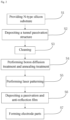
Fig. 2 shows a flow chart of a method for preparing solar cells of the present disclosure. -
Fig. 3 shows the ECV doping curves in the first emitter layer and the second emitter region of the solar cell of Example 1 and the ECV doping concentration-depth curve of a conventional boron emitter. - The present application will be further described in detail below in conjunction with the drawings and examples. Through these descriptions, the features and advantages of the present application will become clear.
- The word "exemplary" as used herein means "serving as an example, example, or illustrative." Any embodiment described herein as "exemplary" is not necessarily to be construed as superior to other embodiments. Although various aspects of the embodiments are illustrated in the drawings, the drawings are not necessarily drawn to scale unless otherwise indicated.
- In addition, the technical features involved in different embodiments of the present application described below can be combined with each other as long as they do not conflict with each other.
- As shown in
Fig. 1 , the present application provides a solar cell, comprising: - an N-
type silicon substrate 1 having a first surface and a second surface, - a
tunnel passivation structure 2 and a first passivation andanti-reflection film 6 formed on the first surface, - a boron-doped emitter structure layer formed on the second surface, wherein the emitter structure layer includes a first emitter layer 3 and a
second emitter region 4, wherein the junction depth of the first emitter layer 3 is smaller than that of thesecond emitter region 4, the highest boron doping concentration of the first emitter layer is greater than that of the second emitter region, and the total boron doping amount of the first emitter layer is less than that of the second emitter region, - a second passivation and
anti-reflection film 5 formed on the emitter structure layer, - a
first electrode 7 configured to be in electrical contact with thesecond emitter region 4, - a
second electrode 8 configured to be in electrical contact with thetunnel passivation structure 2. - In this application, the front surface refers to the surface where sunlight enters, and the back surface refers to the surface opposite to the surface where sunlight enters. In
Fig. 1 , the upper side surface of the N-type silicon substrate 1 is the front surface (second surface), and the lower side surface is the back surface (first surface). - The structure of the solar cell is described below in conjunction with the preparation process. As shown in
Fig. 2 , the solar cell can be prepared as follows. - S1 Providing N-type silicon substrate.
- S2 Depositing a tunnel passivation structure on the first surface of the N-type silicon substrate, and then depositing a mask layer on the tunnel passivation structure.
- S3 Cleaning the second surface of the N-type silicon substrate.
- S4 Performing boron diffusion treatment on the cleaned second surface of the N-type silicon substrate and annealing treatment on the tunnel passivation structure in the same environment, so that a first emitter layer is formed on the second surface of the N-type silicon substrate and the tunnel passivation structure is crystallized.
- S5 Performing laser patterning on the first emitter layer to form a second emitter region.
- S6 Depositing a passivation and anti-reflection film, and
- S7 Forming a first electrode and a second electrode, wherein the first electrode is configured to be in electrical contact with the second emitter region, and the second electrode is configured to be in electrical contact with the tunnel passivation structure.
- Before preparation, the N-type silicon substrate can be cleaned and polished to facilitate subsequent processes.
- After that, as shown in
Fig. 1 , atunnel passivation structure 2 is deposited on the first surface (back surface) of the N-type silicon substrate 1. The tunnel passivation structure may be various tunnel passivation structures that can be used in TOPCon cells. For example, it can include atunnel oxide layer 21 and a passivationcontact material layer 22, wherein thetunnel oxide layer 21 is disposed between the N-type silicon substrate 1 and the passivationcontact material layer 22. In one embodiment, the tunnel oxide layer may be made of silicon oxide or other materials. In one embodiment, the material of the passivation contact material layer is selected from one or more of doped amorphous silicon, doped polysilicon, and silicon carbide material SiCx, such as phosphorus-doped polysilicon layer and silicon carbide material. - Afterwards, a cleaning step is performed on the second surface (front surface) of the N-type silicon substrate to remove unnecessary wrap-around material layers produced on the front surface, such as polysilicon layers. A texturing step can also be performed after cleaning, whereby a textured surface can be formed to increase surface area, reduce surface reflectivity, remove impurities, etc.
- After that, the cleaned second surface of the N-type silicon substrate is subjected to boron diffusion treatment and the tunnel passivation structure is annealed in the same environment, so that a first emitter layer is formed on the second surface of the N-type silicon substrate and the tunnel passivation structure is crystallized. Boron is diffused on the second surface (front surface) of the N-
type silicon substrate 1 to form a p-type silicon layer, that is, the first emitter layer 3. When being processed in the same environment, in addition to boron diffusion on the second surface (front surface) of the N-type silicon substrate to form a p-type silicon layer (first emitter layer 3), the preformedtunnel passivation structure 2 is also simultaneously subjected to an annealing treatment, so that crystallization of the materials in the passivation contact material layer and redistribution of doping elements can be completed during the high-temperature diffusion process of boron, which can improve the passivation capability of the passivation contact structure. Therefore, there is no need to perform a separate annealing treatment step on the tunnel passivation structure, thereby avoiding the adverse effects of the high temperature of the annealing treatment on the silicon wafer and the layers formed thereon. In one embodiment, the boron source used in the boron diffusion treatment can be BCl3, BBr3, etc. In this application, the temperature of the boron diffusion treatment is low and the time is short, and the junction depth of the formed p-type silicon layer (first emitter layer) is relatively small. The junction depth of the first emitter layer 3 can be less than or equal to 0.7µm, which can improve optical response. In one embodiment, the temperature of the same environment is 300-970°C, and the treatment time at 800-970°C is less than 3 hours. In one embodiment, the sheet resistance of the first emitter layer is greater than or equal to 150 ohm/sq. - In one embodiment, the junction depth of the first emitter layer 3 may be less than or equal to 0.7µm, thereby improving the optical response.
Fig. 1 shows the junction depth h1 of the first emitter layer, which is equivalent to the thickness of the first emitter layer, which is the distance from the surface to where the first emitter layer is present. - Afterwards, laser patterning is performed on the first emitter layer 3 to form a
second emitter region 4. The conditions for laser patterning are: using one or two or more wavelengths of laser such as ultraviolet, green or infrared, the pulse width is nanoseconds, picoseconds or femtoseconds, and the average power is 5-200W, for example, green nanosecond laser with a wavelength of 532nm and power of 30W can be used. As shown inFig. 1 , through laser patterning, boron doping can be promoted to form a second emitter region with different junction depth, doping concentration and sheet resistance from the first emitter layer. In this application, the junction depth h1 of the first emitter layer is smaller than the junction depth h2 of the second emitter region.Fig. 1 shows the junction depth h2 of the second emitter region, which is equivalent to the thickness of the second emitter region, which is the distance from the surface to where the second emitter is present. In one embodiment, the junction depth h2 of the second emitter region is greater than or equal to 0.8µm. However, the junction depth h2 of the second emitter region generally does not exceed 5µm. As described later, the second emitter region is in electrical contact with thefirst electrode 7, and the above junction depth h2 can meet the metallization requirements. The first emitter layer 3 and thesecond emitter region 4 together form an emitter structure layer. - For the first emitter layer, the highest point in the ECV doping concentration-depth curve (ECV doping curve) is not on the surface of the silicon wafer, but at an internal position at a depth of about 0.02-0.5µm from the surface of the first emitter layer. Moreover, the change amplitude of the doping curve of the first emitter layer is relatively large, and the doping concentration changes greatly in the depth range of 0.02-0.6µm, and the difference between the highest boron doping concentration and the lowest doping concentration is greater than 1 order of magnitude. For example, the boron doping concentration in the first emitter layer is 2×10¹⁹ to 1×10¹⁸ atm/cm3, or 3×10¹⁹ to 5×10¹⁷ atm/cm3, etc. The steep diffusion junction of the first emitter layer can be achieved using a shorter boron diffusion process time, therefore reducing manufacturing costs.
- For the second emitter region, the ECV doping concentration-depth curve (ECV doping curve) of the second emitter region is flatter, the doping concentration does not change much in the depth range of 0.05-0.7µm, and the difference between the highest boron doping concentration and the lowest boron doping concentration is less than 1 order of magnitude. For example, the boron doping concentration in the second emitter region is 1×10¹⁹-1×10¹⁸ atm/cm3, 5×10¹³-5×10¹⁹ atm/cm3, or 1×10¹⁹-1×10²⁰ atm/cm3. The flatter doped junction in the second emitter region is more conducive to forming a good metal contact and reducing the contact resistivity. It can also reduce the recombination current density in the metal region and improve the photoelectric conversion efficiency of the solar cell.
- In one embodiment, the sheet resistance of the first emitter layer is greater than the sheet resistance of the second emitter region. In one implementation, the sheet resistance of the first emitter layer is greater than or equal to 150 ohm/sq, and the sheet resistance of the second emitter region is less than or equal to 150 ohm/sq.
- Afterwards, the silicon wafer surface is cleaned. This cleaning step can clean the mask layer on the tunnel passivation structure on the back surface and the oxide layer on the front surface. The cleaning step may be implemented by alkali washing and/or acid washing. For example, alkali washing may use potassium hydroxide solution, sodium hydroxide solution, etc. as detergents, and acid washing may use HF solution, HCl solution, etc. as detergents.
- Afterwards, passivation and anti-reflection films are deposited on both surfaces of the silicon wafer. The method of depositing the passivation and anti-reflection films can use various methods known in the art. The material of the passivation and anti-reflection films can be various commonly used passivation and anti-reflection film materials such as combination of one or more of aluminum oxide, silicon oxide, silicon nitride, and silicon oxynitride. The passivation and anti-reflection film can be composed of a single layer of material, or a multi-layer structure composed of multiple layers of materials. As shown in
Fig. 1 , the second passivation andanti-reflection film 5 is located on the front surface, and the first passivation andanti-reflection film 6 is located on the back surface. - After that, metal electrode parts are deposited. As shown in
Fig. 1 , the metal electrode parts include afirst electrode 7 and asecond electrode 8. Thefirst electrode 7 is located on the front surface and is configured to be in electrical contact with thesecond emitter region 4. Thesecond electrode 8 is located on the back surface and is configured to be in electrical contact with thetunnel passivation structure 2, in particular with the passivationcontact material layer 22. Depositing metal electrodes can be done by conventional means such as screen printing. - In one embodiment, as shown in
Fig. 1 , the width of thefirst electrode 7 is smaller than the width of thesecond emitter region 4.Fig. 1 shows the width w1 of thefirst electrode 7 and the width w2 of thesecond emitter region 4, which are the respective edge spacings of thefirst electrode 7 and thesecond emitter region 4 in the x direction. This arrangement has the following advantages: the first electrode region can completely cover the second emitter region, and heavy doping effectively reduces metal recombination under the first electrode region, reduces recombination current density, and increases the open circuit voltage of the cells. - Wet chemical cleaning is performed on n-type silicon wafers to remove surface damage and impurities, and alkali solution is used to polish the surface to form a surface with higher flatness and a reflectivity greater than 30%, which is more suitable for achieving better passivation effect of the passivation contact structure of the back surface.
- A tunnel silicon oxide layer and a doped polysilicon layer are deposited on the back surface of the silicon wafer through PECVD method. The thickness of the tunnel silicon oxide layer is 0.9-2nm and the thickness of the doped polysilicon layer is 75-150nm. Then, a silicon oxide layer mask is further deposited on the outer layer, with thickness of 10-50nm.
- Wet chemical cleaning is used to remove the wrap-around polysilicon layer on the front surface, and then the front surface is subjected to alkali texturing to form a pyramid structure on the front surface of the silicon wafer, while the back surface maintains the original structure under the protection of a mask.
- The silicon wafer is placed in a tubular diffusion furnace tube, and BCl3 and oxygen gas are introduced at a temperature above 800°C. Reaction occurs on the surface of the silicon wafer and boron atoms are formed and then diffused into the interior of the silicon wafer to form the first emitter, and a silicon oxide layer containing rich boron atoms, that is, borosilicate glass BSG is formed on the surface. The conditions for boron diffusion are: in the deposition step, the BCl3 flow rate is 300 sccm, the oxygen gas flow rate is 200 sccm, the temperature is 850°C, and the time is 15 minutes. Then in the process of forming junction, the temperature increases and the temperature is 930°C, time is 30min. The sheet resistance of the first emitter is 150-250ohm/sq, the junction depth of the first emitter is 0.5µm, and the thickness of BSG is 10-150nm. At the same time, under the high temperature and time of boron diffusion, the crystallization of the doped polysilicon layer on the back surface and the redistribution of doping elements are completed, which improves the passivation capability of the passivation contact structure.
- Patterning is implemented to the borosilicate glass of the front surface using long pulse laser or short pulse but high overlap rate laser. The laser power is 30W, the spot width is 60-200µm, and the shape of the spot is circular, elliptical or rectangular. After laser treatment, the sheet resistance dropped to less than 150ohm/sq, the junction depth of the diffused second emitter became greater than or equal to 0.7µm, and the surface doping concentration dropped to 1×1019 cm-3.
- Wet chemical cleaning is performed on the surface of the silicon wafer to remove the BSG layer on the front surface, the laser damage layer, and the mask on the back surface.
- ALD is used to deposit aluminum oxide with a thickness of 2-20nm on the front surface of the silicon wafer. Then PECVD is used to deposit combinations of one or more of silicon oxynitride and silicon oxide with a thickness of 50-200nm on the front surface, thus forming the second passivation and anti-reflection film.
- On the back surface of the silicon wafer, PECVD is used to deposit the combinations of one or more of silicon oxynitride and silicon oxide with a thickness of 30-200 nm, thereby forming the first passivation and anti-reflection film.
- On the back surface, screen printing is used to print finger and busbar electrodes, and on the front surface, screen printing is used to print finger electrodes above the second emitter in the laser processing region. The width of the electrodes on the front surface is less than 50µm. Afterwards, it is sintered at high temperature to form ohmic contact between the metal electrodes and the emitter.
-
Fig. 3 also shows the ECV doping curves in the first emitter layer and the second emitter region of the solar cell obtained in Example 1 (inFig. 3 , the first emitter layer represents the ECV doping curve of the first emitter layer, the second emitter region represents the ECV doping curve of the second emitter region), showing that the first emitter layer has a steep diffusion junction type, while the second emitter region has a flatter doping junction type. - Compared with the solar cell prepared in Example 1 of
CN110299422A , the depth of the first emitter of the solar cell obtained in Example 1 of the present disclosure is smaller, with junction depth less than 0.7µm, and the short-wave response of the cell is improved, and the short-circuit current density is higher, increased from 40.3mA/cm2 to 40.6 mA/cm2. - Compared with the solar cell prepared in Example 1 of
CN110299422A , the depth of the second emitter of the solar cell obtained in Example 1 of the present disclosure after laser doping is deeper, greater than 0.7µm, and the electrode contact resistance is lower, falling from 1.5 ohm/cm2 to 0.9 ohm/cm2. - In the description of this application, it should be noted that the terms "upper", "lower", "inner", "outer", "front", "back", "left", "right", etc. indicate the orientation or position that are based on the working state of the present application. It is only for the convenience of describing the present application and simplifying the description. It does not indicate or imply that the device or component referred to must have a specific orientation, be constructed and operated in a specific orientation. Therefore, it cannot be construed as a limitation of this application.
- The present application has been described above with reference to preferred embodiments, but these embodiments are only exemplary and serve an illustrative purpose. On this basis, various substitutions and improvements can be made to the present application, which all fall within the protection scope of the present application.
Claims (12)
- A solar cell, comprising:an N-type silicon substrate having a first surface and a second surface,a tunnel passivation structure and a first passivation and anti-reflection film formed on the first surface,a boron-doped emitter structure layer formed on the second surface, wherein the emitter structure layer includes a first emitter layer and a second emitter region, wherein the junction depth of the first emitter layer is smaller than that of the second emitter region, the highest boron doping concentration of the first emitter layer is greater than that of the second emitter region, and the total boron doping amount of the first emitter layer is less than that of the second emitter region,a second passivation and anti-reflection film formed on the emitter structure layer,a first electrode configured to be in electrical contact with the second emitter region,a second electrode configured to be in electrical contact with the tunnel passivation structure,wherein within the range of a depth of 0.02-0.6µm from the surface of the first emitter layer in the ECV doping curve of the first emitter layer, the difference between the highest boron doping concentration and the lowest boron doping concentration in the first emitter layer is greater than 1 orders of magnitude, and within the range of 0.05-0.7µm from the surface of the second emitter region in the ECV doping curve of the second emitter region, the difference between the highest boron doping concentration and the lowest boron doping concentration in the second emitter region is less than 1 order of magnitude.
- The solar cell according to claim 1, wherein the tunnel passivation structure includes a tunnel oxide layer and a passivation contact material layer, wherein the tunnel oxide layer is disposed between the N-type silicon substrate and the passivation contact material layer.
- The solar cell according to claim 2, wherein the material of the passivation contact material layer is selected from one or more of doped amorphous silicon, doped polysilicon, and silicon carbide.
- The solar cell according to claim 2, wherein the second electrode is configured to be in electrical contact with the passivation contact material layer.
- The solar cell according to claim 1, wherein the junction depth of the first emitter layer is less than or equal to 0.7µm.
- The solar cell according to claim 1, wherein the junction depth of the second emitter region is greater than or equal to 0.8µm.
- The solar cell according to claim 1, wherein the boron doping concentration of the second emitter region is less than or equal to 2×10¹⁹atm/cm3.
- The solar cell according to claim 7, wherein the highest point in the ECV doping curve of the first emitter layer is at an internal position at a depth of 0.05-0.5 µm from the surface of the first emitter layer.
- The solar cell according to claim 1, wherein the sheet resistance of the first emitter layer is greater than that of the second emitter region.
- The solar cell according to claim 9, wherein the sheet resistance of the first emitter layer is greater than or equal to 150 ohm/sq, and the sheet resistance of the second emitter region is less than or equal to 150 ohm/sq.
- The solar cell according to claim 1, wherein the width of the first electrode is smaller than that of the second emitter region.
- The solar cell according to claim 1, wherein the material of the passivation and anti-reflection film is selected from combinations of one or more of aluminum oxide, silicon oxide, silicon nitride, and silicon oxynitride.
Applications Claiming Priority (1)
| Application Number | Priority Date | Filing Date | Title |
|---|---|---|---|
| CN202310072596.5A CN115799364B (en) | 2023-02-07 | 2023-02-07 | a solar cell |
Publications (3)
| Publication Number | Publication Date |
|---|---|
| EP4415056A1 EP4415056A1 (en) | 2024-08-14 |
| EP4415056B1 true EP4415056B1 (en) | 2025-07-02 |
| EP4415056C0 EP4415056C0 (en) | 2025-07-02 |
Family
ID=85430224
Family Applications (1)
| Application Number | Title | Priority Date | Filing Date |
|---|---|---|---|
| EP23206586.2A Active EP4415056B1 (en) | 2023-02-07 | 2023-10-30 | Solar cells |
Country Status (5)
| Country | Link |
|---|---|
| US (2) | US12062728B1 (en) |
| EP (1) | EP4415056B1 (en) |
| JP (2) | JP7486654B1 (en) |
| CN (2) | CN115799364B (en) |
| AU (2) | AU2023258373B9 (en) |
Families Citing this family (4)
| Publication number | Priority date | Publication date | Assignee | Title |
|---|---|---|---|---|
| US11724220B2 (en) | 2017-02-21 | 2023-08-15 | Cummins Filtration Ip, Inc. | Undulated interlocking housing-endplate interface geometry |
| CN118231487B (en) * | 2024-01-18 | 2025-04-22 | 天合光能股份有限公司 | Solar cell and method for manufacturing the same |
| CN119133292B (en) * | 2024-08-30 | 2026-04-24 | 上饶晶科能源叁号智造有限公司 | Solar cell and photovoltaic module |
| CN121712142A (en) * | 2026-02-11 | 2026-03-20 | Tcl中环新能源科技股份有限公司 | Passivation contact structure and preparation method thereof, solar cell and solar module |
Family Cites Families (31)
| Publication number | Priority date | Publication date | Assignee | Title |
|---|---|---|---|---|
| US20080092944A1 (en) * | 2006-10-16 | 2008-04-24 | Leonid Rubin | Semiconductor structure and process for forming ohmic connections to a semiconductor structure |
| CN102934206B (en) * | 2010-06-10 | 2015-08-05 | 株式会社爱发科 | Solar cell manufacturing device and solar cell manufacturing method |
| CN101937941B (en) * | 2010-08-26 | 2012-07-18 | 常州天合光能有限公司 | Method for manufacturing crystalline silicon solar cell selective emitter junction |
| JP2012151265A (en) * | 2011-01-19 | 2012-08-09 | Sharp Corp | Manufacturing method of solar battery and the solar battery manufactured based on the method |
| KR101969032B1 (en) * | 2011-09-07 | 2019-04-15 | 엘지전자 주식회사 | Solar cell and manufacturing method thereof |
| EP2654090B1 (en) * | 2012-04-17 | 2020-07-08 | LG Electronics, Inc. | Solar cell |
| KR101387718B1 (en) * | 2012-05-07 | 2014-04-22 | 엘지전자 주식회사 | Solar cell and method for manufactruing the same |
| JP2014197578A (en) * | 2013-03-29 | 2014-10-16 | パナソニック株式会社 | Method for manufacturing solar cell |
| CN109599450A (en) * | 2013-04-03 | 2019-04-09 | Lg电子株式会社 | Solar cell |
| JP2014229851A (en) * | 2013-05-27 | 2014-12-08 | 住友重機械工業株式会社 | Method for manufacturing solar cell |
| WO2016080348A1 (en) * | 2014-11-21 | 2016-05-26 | 三菱電機株式会社 | Solar cell manufacturing method, and solar cell |
| KR102272433B1 (en) * | 2015-06-30 | 2021-07-05 | 엘지전자 주식회사 | Solar cell and method of manufacturing the same |
| CN110061096B (en) * | 2016-01-29 | 2023-02-28 | 上饶市晶科绿能科技发展有限公司 | Method of making solar cells |
| CN108258082B (en) * | 2018-01-10 | 2021-06-04 | 张家港协鑫集成科技有限公司 | Preparation method of solar cell |
| DE102018123397A1 (en) * | 2018-09-24 | 2020-03-26 | Fraunhofer-Gesellschaft zur Förderung der angewandten Forschung e.V. | Process for the production of a photovoltaic solar cell with a heterojunction and a diffused emitter region |
| CN110299422B (en) | 2019-06-28 | 2021-05-28 | 天合光能股份有限公司 | A kind of laser boron doped selective emitter TOPCon structure battery and preparation method thereof |
| CN110600558B (en) * | 2019-07-27 | 2021-06-25 | 江苏顺风光电科技有限公司 | A Boron Process for P+ Selective Emitter Cells |
| CN111106188B (en) * | 2019-12-17 | 2022-03-18 | 晶澳(扬州)太阳能科技有限公司 | N-type battery, preparation method of selective emitter of N-type battery and N-type battery |
| CN111162145A (en) * | 2020-02-26 | 2020-05-15 | 泰州中来光电科技有限公司 | Passivated contact solar cell with selective emitter structure and preparation method thereof |
| CN111952409B (en) * | 2020-06-30 | 2022-04-19 | 泰州中来光电科技有限公司 | Preparation method of passivated contact battery with selective emitter structure |
| TWM606270U (en) * | 2020-10-08 | 2021-01-01 | 聯合再生能源股份有限公司 | Tunnel oxide passivated contact solar cell |
| CN112331742B (en) * | 2020-11-10 | 2024-11-08 | 帝尔激光科技(无锡)有限公司 | A selective emitter passivation contact solar cell and its preparation method |
| CN112582485B (en) | 2020-12-15 | 2024-04-09 | 泰州隆基乐叶光伏科技有限公司 | Solar cell and manufacturing method thereof |
| CN112670353A (en) * | 2020-12-17 | 2021-04-16 | 浙江正泰太阳能科技有限公司 | Boron-doped selective emitter battery and preparation method thereof |
| CN116314356A (en) * | 2021-02-23 | 2023-06-23 | 浙江晶科能源有限公司 | Solar cell and manufacturing method thereof, solar module |
| CN113809201B (en) * | 2021-08-20 | 2024-09-06 | 西安隆基乐叶光伏科技有限公司 | Boron diffusion method and solar cell |
| CN115020544A (en) * | 2022-06-08 | 2022-09-06 | 中节能太阳能科技(镇江)有限公司 | Fabrication method of boron-doped selective emitter N-type TOPCon cell |
| CN115036391A (en) * | 2022-06-24 | 2022-09-09 | 韩华新能源(启东)有限公司 | Preparation method of N-type solar cell with selective emitter and cell |
| CN115172523A (en) * | 2022-07-13 | 2022-10-11 | 东方日升新能源股份有限公司 | Preparation method of solar cell |
| CN115440839A (en) * | 2022-09-23 | 2022-12-06 | 通威太阳能(眉山)有限公司 | Solar cell and preparation method thereof |
| CN115642202A (en) * | 2022-10-13 | 2023-01-24 | 三一硅能(株洲)有限公司 | Back junction solar cell and preparation method thereof |
-
2023
- 2023-02-07 CN CN202310072596.5A patent/CN115799364B/en active Active
- 2023-02-07 CN CN202310486448.8A patent/CN116314472A/en active Pending
- 2023-10-30 JP JP2023185271A patent/JP7486654B1/en active Active
- 2023-10-30 EP EP23206586.2A patent/EP4415056B1/en active Active
- 2023-10-31 AU AU2023258373A patent/AU2023258373B9/en active Active
- 2023-11-07 US US18/387,556 patent/US12062728B1/en active Active
-
2024
- 2024-05-07 JP JP2024075117A patent/JP7742912B2/en active Active
- 2024-06-26 US US18/754,963 patent/US20240347655A1/en active Pending
- 2024-08-29 AU AU2024216432A patent/AU2024216432B2/en active Active
Also Published As
| Publication number | Publication date |
|---|---|
| JP2024112320A (en) | 2024-08-20 |
| US20240347655A1 (en) | 2024-10-17 |
| AU2023258373B9 (en) | 2024-08-01 |
| JP2024112278A (en) | 2024-08-20 |
| US12062728B1 (en) | 2024-08-13 |
| CN115799364A (en) | 2023-03-14 |
| AU2024216432A1 (en) | 2024-09-19 |
| JP7742912B2 (en) | 2025-09-22 |
| JP7486654B1 (en) | 2024-05-17 |
| AU2024216432B2 (en) | 2025-02-27 |
| EP4415056A1 (en) | 2024-08-14 |
| CN115799364B (en) | 2023-05-26 |
| CN116314472A (en) | 2023-06-23 |
| EP4415056C0 (en) | 2025-07-02 |
| US20240266451A1 (en) | 2024-08-08 |
| AU2023258373B1 (en) | 2024-06-13 |
Similar Documents
| Publication | Publication Date | Title |
|---|---|---|
| JP7747902B2 (en) | Low-cost contact-passivated all-back contact solar cells and methods for fabricating same | |
| CN110838536B (en) | Back contact solar cell with multiple tunnel junction structures and preparation method thereof | |
| CN115513307B (en) | Back contact solar cell and method for preparing the same | |
| EP4415056A1 (en) | Solar cells | |
| WO2024109293A1 (en) | Double-sided tunneling silicon oxide passivated back-contact solar cell and manufacturing method therefor | |
| WO2024114031A1 (en) | Back contact cell, fabrication method therefor, and photovoltaic module | |
| CN120239369A (en) | Back contact solar cell and method for preparing the same | |
| KR102132740B1 (en) | Solar cell and method for manufacutring the same | |
| CN114497290A (en) | Manufacturing method of back contact heterojunction solar cell | |
| CN210778636U (en) | Back contact solar cell with multiple tunnel junction structures | |
| CN112635591A (en) | Preparation method of solar cell and solar cell | |
| EP4239690A2 (en) | Solar cell and preparation method thereof | |
| CN116314471A (en) | A kind of back SE structure preparation method | |
| CN219350237U (en) | Solar cell | |
| JP2025535005A (en) | Back contact solar cell and its manufacturing method | |
| CN114639744A (en) | Solar cell and preparation method thereof | |
| CN115528130A (en) | A kind of preparation method of novel Topcon battery adopting electroplating process metallization | |
| CN116435385A (en) | A kind of TOPCon battery and preparation method thereof | |
| WO2026032089A1 (en) | Solar cell, preparation method therefor and use thereof | |
| WO2025073223A1 (en) | Solar cell, solar module and preparation method for solar cell | |
| CN118231489A (en) | A p-type TOPCon battery and preparation method thereof | |
| CN116469945B (en) | TOPCon battery and preparation method thereof | |
| CN115692517A (en) | A kind of P-type Topcon back-junction battery metallized by electroplating process and preparation method thereof | |
| CN111403534A (en) | A kind of solar cell and preparation method thereof | |
| CN114784139A (en) | Solar cell and method for manufacturing same |
Legal Events
| Date | Code | Title | Description |
|---|---|---|---|
| PUAI | Public reference made under article 153(3) epc to a published international application that has entered the european phase |
Free format text: ORIGINAL CODE: 0009012 |
|
| STAA | Information on the status of an ep patent application or granted ep patent |
Free format text: STATUS: REQUEST FOR EXAMINATION WAS MADE |
|
| 17P | Request for examination filed |
Effective date: 20231030 |
|
| AK | Designated contracting states |
Kind code of ref document: A1 Designated state(s): AL AT BE BG CH CY CZ DE DK EE ES FI FR GB GR HR HU IE IS IT LI LT LU LV MC ME MK MT NL NO PL PT RO RS SE SI SK SM TR |
|
| REG | Reference to a national code |
Ref country code: DE Ref legal event code: R079 Free format text: PREVIOUS MAIN CLASS: H01L0031021600 Ipc: H10F0010166000 Ref country code: DE Ref legal event code: R079 Ref document number: 602023004505 Country of ref document: DE Free format text: PREVIOUS MAIN CLASS: H01L0031021600 Ipc: H10F0010166000 |
|
| GRAP | Despatch of communication of intention to grant a patent |
Free format text: ORIGINAL CODE: EPIDOSNIGR1 |
|
| STAA | Information on the status of an ep patent application or granted ep patent |
Free format text: STATUS: GRANT OF PATENT IS INTENDED |
|
| RIC1 | Information provided on ipc code assigned before grant |
Ipc: H10F 77/30 20250101ALI20250108BHEP Ipc: H10F 77/20 20250101ALI20250108BHEP Ipc: H10F 71/00 20250101ALI20250108BHEP Ipc: H10F 10/166 20250101AFI20250108BHEP |
|
| INTG | Intention to grant announced |
Effective date: 20250203 |
|
| RAP3 | Party data changed (applicant data changed or rights of an application transferred) |
Owner name: TRINA SOLAR (SUQIAN) PHOTOELECTRIC CO., LTD. Owner name: TRINA SOLAR CO., LTD |
|
| GRAS | Grant fee paid |
Free format text: ORIGINAL CODE: EPIDOSNIGR3 |
|
| GRAA | (expected) grant |
Free format text: ORIGINAL CODE: 0009210 |
|
| STAA | Information on the status of an ep patent application or granted ep patent |
Free format text: STATUS: THE PATENT HAS BEEN GRANTED |
|
| RAP3 | Party data changed (applicant data changed or rights of an application transferred) |
Owner name: TRINA SOLAR (SUQIAN) PHOTOELECTRIC CO., LTD. Owner name: TRINA SOLAR CO., LTD. |
|
| AK | Designated contracting states |
Kind code of ref document: B1 Designated state(s): AL AT BE BG CH CY CZ DE DK EE ES FI FR GB GR HR HU IE IS IT LI LT LU LV MC ME MK MT NL NO PL PT RO RS SE SI SK SM TR |
|
| REG | Reference to a national code |
Ref country code: GB Ref legal event code: FG4D |
|
| REG | Reference to a national code |
Ref country code: CH Ref legal event code: EP |
|
| REG | Reference to a national code |
Ref country code: DE Ref legal event code: R096 Ref document number: 602023004505 Country of ref document: DE |
|
| REG | Reference to a national code |
Ref country code: IE Ref legal event code: FG4D |
|
| U01 | Request for unitary effect filed |
Effective date: 20250724 |
|
| U07 | Unitary effect registered |
Designated state(s): AT BE BG DE DK EE FI FR IT LT LU LV MT NL PT RO SE SI Effective date: 20250731 |
|
| U20 | Renewal fee for the european patent with unitary effect paid |
Year of fee payment: 3 Effective date: 20251020 |
|
| PG25 | Lapsed in a contracting state [announced via postgrant information from national office to epo] |
Ref country code: IS Free format text: LAPSE BECAUSE OF FAILURE TO SUBMIT A TRANSLATION OF THE DESCRIPTION OR TO PAY THE FEE WITHIN THE PRESCRIBED TIME-LIMIT Effective date: 20251102 |
|
| PG25 | Lapsed in a contracting state [announced via postgrant information from national office to epo] |
Ref country code: NO Free format text: LAPSE BECAUSE OF FAILURE TO SUBMIT A TRANSLATION OF THE DESCRIPTION OR TO PAY THE FEE WITHIN THE PRESCRIBED TIME-LIMIT Effective date: 20251002 |
|
| PG25 | Lapsed in a contracting state [announced via postgrant information from national office to epo] |
Ref country code: HR Free format text: LAPSE BECAUSE OF FAILURE TO SUBMIT A TRANSLATION OF THE DESCRIPTION OR TO PAY THE FEE WITHIN THE PRESCRIBED TIME-LIMIT Effective date: 20250702 |
|
| PG25 | Lapsed in a contracting state [announced via postgrant information from national office to epo] |
Ref country code: GR Free format text: LAPSE BECAUSE OF FAILURE TO SUBMIT A TRANSLATION OF THE DESCRIPTION OR TO PAY THE FEE WITHIN THE PRESCRIBED TIME-LIMIT Effective date: 20251003 |
|
| PG25 | Lapsed in a contracting state [announced via postgrant information from national office to epo] |
Ref country code: CZ Free format text: LAPSE BECAUSE OF FAILURE TO SUBMIT A TRANSLATION OF THE DESCRIPTION OR TO PAY THE FEE WITHIN THE PRESCRIBED TIME-LIMIT Effective date: 20250702 |
|
| PG25 | Lapsed in a contracting state [announced via postgrant information from national office to epo] |
Ref country code: PL Free format text: LAPSE BECAUSE OF FAILURE TO SUBMIT A TRANSLATION OF THE DESCRIPTION OR TO PAY THE FEE WITHIN THE PRESCRIBED TIME-LIMIT Effective date: 20250702 |
|
| PG25 | Lapsed in a contracting state [announced via postgrant information from national office to epo] |
Ref country code: RS Free format text: LAPSE BECAUSE OF FAILURE TO SUBMIT A TRANSLATION OF THE DESCRIPTION OR TO PAY THE FEE WITHIN THE PRESCRIBED TIME-LIMIT Effective date: 20251002 |
|
| PG25 | Lapsed in a contracting state [announced via postgrant information from national office to epo] |
Ref country code: ES Free format text: LAPSE BECAUSE OF FAILURE TO SUBMIT A TRANSLATION OF THE DESCRIPTION OR TO PAY THE FEE WITHIN THE PRESCRIBED TIME-LIMIT Effective date: 20250702 |
|
| PG25 | Lapsed in a contracting state [announced via postgrant information from national office to epo] |
Ref country code: SM Free format text: LAPSE BECAUSE OF FAILURE TO SUBMIT A TRANSLATION OF THE DESCRIPTION OR TO PAY THE FEE WITHIN THE PRESCRIBED TIME-LIMIT Effective date: 20250702 |
|
| PG25 | Lapsed in a contracting state [announced via postgrant information from national office to epo] |
Ref country code: SK Free format text: LAPSE BECAUSE OF FAILURE TO SUBMIT A TRANSLATION OF THE DESCRIPTION OR TO PAY THE FEE WITHIN THE PRESCRIBED TIME-LIMIT Effective date: 20250702 |
|
| PLBE | No opposition filed within time limit |
Free format text: ORIGINAL CODE: 0009261 |
|
| STAA | Information on the status of an ep patent application or granted ep patent |
Free format text: STATUS: NO OPPOSITION FILED WITHIN TIME LIMIT |