EP4415037A1 - Formation d'un composant electronique de puissance - Google Patents
Formation d'un composant electronique de puissance Download PDFInfo
- Publication number
- EP4415037A1 EP4415037A1 EP24155576.2A EP24155576A EP4415037A1 EP 4415037 A1 EP4415037 A1 EP 4415037A1 EP 24155576 A EP24155576 A EP 24155576A EP 4415037 A1 EP4415037 A1 EP 4415037A1
- Authority
- EP
- European Patent Office
- Prior art keywords
- layer
- face
- oxygen
- doped polysilicon
- semiconductor substrate
- Prior art date
- Legal status (The legal status is an assumption and is not a legal conclusion. Google has not performed a legal analysis and makes no representation as to the accuracy of the status listed.)
- Withdrawn
Links
Images



Classifications
-
- H—ELECTRICITY
- H10—SEMICONDUCTOR DEVICES; ELECTRIC SOLID-STATE DEVICES NOT OTHERWISE PROVIDED FOR
- H10D—INORGANIC ELECTRIC SEMICONDUCTOR DEVICES
- H10D18/00—Thyristors
- H10D18/01—Manufacture or treatment
-
- H—ELECTRICITY
- H10—SEMICONDUCTOR DEVICES; ELECTRIC SOLID-STATE DEVICES NOT OTHERWISE PROVIDED FOR
- H10D—INORGANIC ELECTRIC SEMICONDUCTOR DEVICES
- H10D18/00—Thyristors
- H10D18/80—Bidirectional devices, e.g. triacs
-
- H—ELECTRICITY
- H10—SEMICONDUCTOR DEVICES; ELECTRIC SOLID-STATE DEVICES NOT OTHERWISE PROVIDED FOR
- H10W—GENERIC PACKAGES, INTERCONNECTIONS, CONNECTORS OR OTHER CONSTRUCTIONAL DETAILS OF DEVICES COVERED BY CLASS H10
- H10W74/00—Encapsulations, e.g. protective coatings
- H10W74/40—Encapsulations, e.g. protective coatings characterised by their materials
- H10W74/43—Encapsulations, e.g. protective coatings characterised by their materials comprising oxides, nitrides or carbides, e.g. ceramics or glasses
-
- H—ELECTRICITY
- H10—SEMICONDUCTOR DEVICES; ELECTRIC SOLID-STATE DEVICES NOT OTHERWISE PROVIDED FOR
- H10D—INORGANIC ELECTRIC SEMICONDUCTOR DEVICES
- H10D18/00—Thyristors
-
- H—ELECTRICITY
- H10—SEMICONDUCTOR DEVICES; ELECTRIC SOLID-STATE DEVICES NOT OTHERWISE PROVIDED FOR
- H10D—INORGANIC ELECTRIC SEMICONDUCTOR DEVICES
- H10D18/00—Thyristors
- H10D18/01—Manufacture or treatment
- H10D18/021—Manufacture or treatment of bidirectional devices, e.g. triacs
-
- H—ELECTRICITY
- H10—SEMICONDUCTOR DEVICES; ELECTRIC SOLID-STATE DEVICES NOT OTHERWISE PROVIDED FOR
- H10D—INORGANIC ELECTRIC SEMICONDUCTOR DEVICES
- H10D64/00—Electrodes of devices having potential barriers
- H10D64/01—Manufacture or treatment
- H10D64/013—Manufacture or treatment of electrodes having a conductor capacitively coupled to a semiconductor by an insulator
- H10D64/01302—Manufacture or treatment of electrodes having a conductor capacitively coupled to a semiconductor by an insulator the insulator being formed after the semiconductor body, the semiconductor being silicon
- H10D64/01304—Manufacture or treatment of electrodes having a conductor capacitively coupled to a semiconductor by an insulator the insulator being formed after the semiconductor body, the semiconductor being silicon characterised by the conductor
- H10D64/01306—Manufacture or treatment of electrodes having a conductor capacitively coupled to a semiconductor by an insulator the insulator being formed after the semiconductor body, the semiconductor being silicon characterised by the conductor the conductor comprising a layer of silicon contacting the insulator, e.g. polysilicon
-
- H—ELECTRICITY
- H10—SEMICONDUCTOR DEVICES; ELECTRIC SOLID-STATE DEVICES NOT OTHERWISE PROVIDED FOR
- H10P—GENERIC PROCESSES OR APPARATUS FOR THE MANUFACTURE OR TREATMENT OF DEVICES COVERED BY CLASS H10
- H10P14/00—Formation of materials, e.g. in the shape of layers or pillars
- H10P14/60—Formation of materials, e.g. in the shape of layers or pillars of insulating materials
- H10P14/65—Formation of materials, e.g. in the shape of layers or pillars of insulating materials characterised by treatments performed before or after the formation of the materials
- H10P14/6516—Formation of materials, e.g. in the shape of layers or pillars of insulating materials characterised by treatments performed before or after the formation of the materials of treatments performed after formation of the materials
- H10P14/6518—Formation of materials, e.g. in the shape of layers or pillars of insulating materials characterised by treatments performed before or after the formation of the materials of treatments performed after formation of the materials by introduction of substances into an already-existing insulating layer
- H10P14/6519—Formation of materials, e.g. in the shape of layers or pillars of insulating materials characterised by treatments performed before or after the formation of the materials of treatments performed after formation of the materials by introduction of substances into an already-existing insulating layer the substance being oxygen
-
- H—ELECTRICITY
- H10—SEMICONDUCTOR DEVICES; ELECTRIC SOLID-STATE DEVICES NOT OTHERWISE PROVIDED FOR
- H10W—GENERIC PACKAGES, INTERCONNECTIONS, CONNECTORS OR OTHER CONSTRUCTIONAL DETAILS OF DEVICES COVERED BY CLASS H10
- H10W74/00—Encapsulations, e.g. protective coatings
- H10W74/10—Encapsulations, e.g. protective coatings characterised by their shape or disposition
- H10W74/131—Encapsulations, e.g. protective coatings characterised by their shape or disposition the semiconductor body being only partially enclosed
- H10W74/134—Encapsulations, e.g. protective coatings characterised by their shape or disposition the semiconductor body being only partially enclosed the encapsulations being in grooves in the semiconductor body
-
- H—ELECTRICITY
- H10—SEMICONDUCTOR DEVICES; ELECTRIC SOLID-STATE DEVICES NOT OTHERWISE PROVIDED FOR
- H10W—GENERIC PACKAGES, INTERCONNECTIONS, CONNECTORS OR OTHER CONSTRUCTIONAL DETAILS OF DEVICES COVERED BY CLASS H10
- H10W74/00—Encapsulations, e.g. protective coatings
- H10W74/10—Encapsulations, e.g. protective coatings characterised by their shape or disposition
- H10W74/131—Encapsulations, e.g. protective coatings characterised by their shape or disposition the semiconductor body being only partially enclosed
- H10W74/137—Encapsulations, e.g. protective coatings characterised by their shape or disposition the semiconductor body being only partially enclosed the encapsulations being directly on the semiconductor body
-
- H—ELECTRICITY
- H10—SEMICONDUCTOR DEVICES; ELECTRIC SOLID-STATE DEVICES NOT OTHERWISE PROVIDED FOR
- H10W—GENERIC PACKAGES, INTERCONNECTIONS, CONNECTORS OR OTHER CONSTRUCTIONAL DETAILS OF DEVICES COVERED BY CLASS H10
- H10W74/00—Encapsulations, e.g. protective coatings
- H10W74/10—Encapsulations, e.g. protective coatings characterised by their shape or disposition
- H10W74/131—Encapsulations, e.g. protective coatings characterised by their shape or disposition the semiconductor body being only partially enclosed
- H10W74/141—Encapsulations, e.g. protective coatings characterised by their shape or disposition the semiconductor body being only partially enclosed the encapsulations being on at least the sidewalls of the semiconductor body
-
- H—ELECTRICITY
- H10—SEMICONDUCTOR DEVICES; ELECTRIC SOLID-STATE DEVICES NOT OTHERWISE PROVIDED FOR
- H10W—GENERIC PACKAGES, INTERCONNECTIONS, CONNECTORS OR OTHER CONSTRUCTIONAL DETAILS OF DEVICES COVERED BY CLASS H10
- H10W74/00—Encapsulations, e.g. protective coatings
- H10W74/10—Encapsulations, e.g. protective coatings characterised by their shape or disposition
- H10W74/131—Encapsulations, e.g. protective coatings characterised by their shape or disposition the semiconductor body being only partially enclosed
- H10W74/147—Encapsulations, e.g. protective coatings characterised by their shape or disposition the semiconductor body being only partially enclosed the encapsulations being multilayered
-
- H—ELECTRICITY
- H10—SEMICONDUCTOR DEVICES; ELECTRIC SOLID-STATE DEVICES NOT OTHERWISE PROVIDED FOR
- H10P—GENERIC PROCESSES OR APPARATUS FOR THE MANUFACTURE OR TREATMENT OF DEVICES COVERED BY CLASS H10
- H10P52/00—Grinding, lapping or polishing of wafers, substrates or parts of devices
Definitions
- This description relates generally to semiconductor electronic components and more particularly to power electronic components such as thyristors and triacs.
- MESA technology which consists of surrounding a PN junction, formed over the entire surface of the component, with a groove (also called a trench) filled with glass on at least one face of the component as a termination of the junction.
- the method comprises, between steps b) and c), a step e) of depositing an electrically insulating layer on and in contact with the oxygen-doped polysilicon layer.
- the method comprises, between steps c) and d), a step e) of depositing an electrically insulating layer on and in contact with the glass layer and a portion of the oxygen-doped polysilicon layer not covered by the glass layer.
- the electrically insulating layer is etched, at the same time as the oxygen-doped polysilicon layer during step d).
- the deposition of the glass layer during step c) is carried out by screen printing.
- the groove has a depth greater than 75 ⁇ m.
- the oxygen-doped polysilicon layer has a thickness of between 0.1 ⁇ m and 2 ⁇ m.
- the component comprises an electrically insulating layer between the oxygen-doped polysilicon layer and the glass layer, the electrically insulating layer being in contact, by a first face, with the oxygen-doped polysilicon layer and, by a second face opposite the first face, with the glass layer.
- the component comprises an electrically insulating layer, the glass layer being in contact, by a first face, with the electrically insulating layer and, by a second face opposite the first face, with the oxygen-doped polysilicon layer and the electrically insulating layer being in contact with a portion of the oxygen-doped polysilicon layer not covered by the glass layer.
- the groove has a depth greater than 75 ⁇ m.
- the oxygen-doped polysilicon layer has a thickness of between 0.1 ⁇ m and 2 ⁇ m.
- Another embodiment provides a power control circuit comprising a power electronic component as described.
- the expressions “approximately”, “approximately”, “substantially”, and “of the order of” mean to within 10%, preferably to within 5%.
- So-called vertical power electronic components generally comprise a semiconductor substrate comprising at least one horizontal planar PN junction surrounded laterally by a peripheral groove extending vertically in the substrate.
- vertical power electronic components must comprise a passivation structure covering the sides and bottom of the groove and part of one face of the semiconductor substrate, on the surface of the groove.
- the passivation structure may for example comprise a layer of oxygen-doped polysilicon or SIPOS (from the English "Semi-Insulating Polycrystalline Silicon").
- SIPOS oxygen-doped polysilicon
- the passivation structure may, in addition, comprise a glass layer formed on the SIPOS layer and more precisely formed in the groove and on said face of the semiconductor substrate, on the surface of the groove, such that it completely covers the SIPOS layer.
- the depth of the groove creates complexity in the etching of the SIPOS layer which is carried out before the formation of the glass layer. More particularly, it creates complexity in the formation of the masking resin through which the SIPOS layer is etched, in particular its structuring by photolithography. Indeed, the deposition of the masking resin is not uniform and a significant amount of resin must be deposited so that the top of the groove is covered by the resin. In some cases, the thickness of the resin on the upper face of the substrate is such that a single photolithography step does not allow it to be locally exposed throughout its thickness.
- the depth of the groove can be greater than a hundred micrometers and the thickness of the masking resin can reach several tens of micrometers.
- several cycles of deposition and then exposure of the resin may be necessary to obtain the desired thickness. This results in increased complexity and an increase in the cost of manufacturing the components.
- the described power electronic components can, for example, be used in various power control, conversion or adaptation circuits, for example in industrial equipment, display or lighting devices, telecommunications equipment, household appliances, automotive devices, etc.
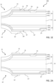
- FIG. 1A , there Figure 1B , there Figure 1C , there Figure 1D and the Figure 1E represent, by means of partial and schematic sectional views, successive stages of an example of a manufacturing process for a component of power according to a first embodiment.
- the Figures 1A to 1E more particularly illustrate an example of a method for forming a peripheral passivation structure of a power component according to the first embodiment. It will be noted that in the figures, the production of a single component is shown. In practice, a plurality of components can be formed simultaneously in and on the same semiconductor substrate, the substrate then being cut into individual chips each comprising a single power electronic component.
- FIG. 1A represents a starting structure comprising a semiconductor substrate 13 in which is formed, on the side of its upper face, a peripheral groove 15 laterally surrounding a horizontal planar PN junction of the component.
- Figure 1A only a part of the starting structure has been shown. In practice the structure extends beyond the right edge shown in dotted lines in Figure 1A , the peripheral groove 15 surrounding the structure.
- the component has, for example, when viewed from above, a general square or rectangular shape, for example with rounded corners, or circular.
- the substrate 13 is, for example, made of silicon.
- the substrate 13 comprises a central portion 17, for example doped with a first type of conductivity, for example doped with type N.
- the substrate 13 further comprises an upper portion 19, for example doped with a second type of conductivity different from the first type of conductivity, for example doped with type P.
- the upper portion 19 is in contact, by its lower face with the upper face of the central portion 17 of the substrate 13.
- the upper part 19 of the substrate 13 comprises, for example, a doping gradient increasing from its lower face.
- the upper part 19 of the substrate 13 comprises, for example, several different doping elements.
- the upper part 19 of the substrate 13 comprises a first portion 191, in contact, by its lower face with the upper face of the part 17 of the substrate 13.
- the first portion 191 is for example doped with aluminum atoms.
- the upper part 19 of the substrate 13 comprises for example a second portion 193, in contact, by its lower face with the upper face of the portion 191.
- the second portion 193 is for example doped with gallium atoms.
- the upper part 19 of the substrate 13 further comprises a third portion 195, in contact, by its lower face with the upper face of the portion 193.
- the third portion 195 is for example doped with gallium atoms.
- the groove 15 formed on the upper face of the starting structure extends from the upper face of the upper part 19 of the substrate 13 into the substrate 13 and opens into the first part 17 of the substrate 13.
- the groove thus extends, for example, through the portions 195, 193 and 191.
- the groove 15 crosses the PN junction formed by the horizontal interface plane between the upper 19 and central 17 parts.
- the depth of the groove 15 from the upper face of the substrate 13 is for example greater than 30 ⁇ m, for example greater than 75 ⁇ m, for example greater than 105 ⁇ m, for example between 105 ⁇ m and 150 ⁇ m.
- the structure of the Figure 1A further comprises a layer 21 of oxygen-doped polysilicon or SIPOS (from the English "Semi-Insulating Polycrystalline Silicon"), extending over the walls of the grooves 15 and on and in contact with the upper face of the substrate 13, at the surface of the grooves 15.
- SIPOS layer 21 has an oxygen percentage of between 10% and 50%, for example of between 20% and 40%.
- the SIPOS layer 21 is, for example, deposited on the surface of the substrate 13 and in the grooves 15 by a chemical vapor deposition process, for example by a low pressure chemical vapor deposition process or LPCVD.
- the SIPOS layer 21 has a thickness of between 0.1 ⁇ m and 2 ⁇ m, for example between 0.1 ⁇ m and 1 ⁇ m, for example of the order of 0.5 ⁇ m.
- the starting structure illustrated in Figure 1A is for example horizontally symmetrical.
- the substrate 13 comprises for example a lower part 23 comprising portions 231, 233 and 235 for example respectively similar to the portions 191, 193 and 195 of the upper part 19.
- the structure comprises for example a groove 15' formed from the lower face of the substrate 13.
- the groove 15' extends in the lower part 23 and opens into the central part 17 of the substrate 13.
- the starting structure comprises for example another SIPOS layer 21' extending on and in contact with the lower face of the substrate 13 and on the walls of the groove 15' formed from the lower face of the substrate 13.
- the groove 15' crosses the PN junction formed by the horizontal interface plane between the lower 23 and central 17 parts of the substrate.
- the starting structure further comprises a localized doped zone 25 on the side of the upper face of the substrate 13, flush with this same face.
- the structure may further comprise a localized doped zone 27 on the side of the lower face of the substrate 13, flush with this same face.
- layers 17, 19 and 23 each extend over the entire surface of the substrate.
- Zones 25 and 27 are respectively located on only a part of the surface of the substrate.
- Areas 25 and 27 are, for example, doped with the first conductivity type, for example N type. For example, areas 25 and 27 are more heavily doped than central portion 17 of substrate 13 and than portions 195 and 235 of substrate 13. For example, areas 25 and 27 are doped with phosphorus atoms.
- the starting structure is thus constituted by a first vertical stack of four regions 19, 17, 23, and 27 alternately doped P and N, and a second vertical stack of four regions 25, 19, 17, and 23 alternately doped N and P, which define a triac.
- region 27 can be omitted in the case of a thyristor type structure.
- the embodiments described can be applied to any so-called vertical power electronic component, comprising a horizontal PN junction and a passivation structure formed in a peripheral insulation groove vertically crossing the PN junction.
- FIG. 1B illustrates a structure obtained at the end of a step of forming an electrically insulating layer 29 on the upper face of the structure illustrated in Figure 1A .
- an electrically insulating layer 29' is further formed on the underside of the structure.
- layer 29 is formed as a full plate, that is to say it is formed on the entire upper face of the structure illustrated in Figure 1A .
- the layer 29 is formed in contact with the SIPOS layer 21.
- the layer 29 covers, for example, the upper face of the layer 21 located on the sides and in the bottom of the groove 15 and extending to the surface of the groove 15.
- layer 29' is formed as a full plate, that is, it is formed over the entire underside of the structure illustrated in Figure 1A .
- the layer 29' is formed in contact with the SIPOS layer 21'.
- the layer 29' covers for example the lower face of the layer 21' located on the sides and in the bottom of the groove 15' and extending to the surface of the groove 15'.
- layers 29 and 29' are made of undoped glass, for example undoped silicon glass (USG) or undoped phosphosilicate glass (PSG).
- Layers 29 and 29' are for example deposited by a chemical vapor deposition process, for example by an LPCVD deposition process.
- layers 29 and 29' have a thickness of between 0.1 ⁇ m and 1.5 ⁇ m, for example between 0.5 ⁇ m and 1 ⁇ m.
- FIG. 1C illustrates a structure obtained at the end of a step of forming a glass layer 31 on the upper face of the structure illustrated in Figure 1B .
- a glass layer 31' is further formed on the underside of the structure.
- the layer 31 is formed locally on the surface of the layer 29 and, for example, in contact with it.
- the layer 31 thus covers layer 29 located in the bottom and on the sides of the groove 15 and on the surface of the groove 15 without extending over the entire surface of the layer 29 on the surface of the groove 15.
- the layer 31' is formed locally on the surface of the layer 29' and, for example, in contact with it.
- the layer 31' thus covers the layer 29' located in the bottom and on the sides of the groove 15' and on the surface of the groove 15' without extending over the entire surface of the layer 29' on the surface of the groove 15'.
- the layers 31 and 31' are deposited by a localized deposition process, for example by screen printing. This step consists for example in the deposition of a glass paste through a mask located on the surface of the layer 29 or the layer 29'.
- the annealing step may for example comprise a pyrolysis step at a temperature between 300°C and 700°C, for example of the order of 500°C.
- the annealing step may further comprise a sintering step at a temperature between 500°C and 1000°C, for example of the order of 800°C.
- layers 31 and 31' have a thickness that is not constant over all of their surfaces. For example, it is greater at the bottom of grooves 15 and 15' (i.e. in the grooves of the wafer between the components) than at their top and at the surface of grooves 15 and 15'.
- the thickness of the layers 31 and 31' on the surface of the substrate 13 at the periphery of the grooves 15 and 15' is for example between 10 ⁇ m and 40 ⁇ m, for example between 20 ⁇ m and 30 ⁇ m.
- the thickness of the layers 31 and 31' in the bottom of the grooves 15 and 15' is for example between 20 ⁇ m and 70 ⁇ m, for example between 40 ⁇ m and 50 ⁇ m.
- FIG. 1D illustrates a structure obtained following a step of localized removal of layers 21 and 29 and layers 21' and 29' of the structure illustrated in Figure 1C .
- the photosensitive resin of the masking layer is deposited by spin-coating, exposed to UV and then developed in a solvent.
- the masking layer covers the entire surface of the glass layer 31.
- the masking layer also extends laterally beyond the glass layer 31, and thus covers a portion of the layers 21 and 29 in the vicinity of the glass layer 31.
- the masking layer does not cover the layers 21 and 29 opposite a central portion of the component.
- layers 21 and 29 are etched through the masking layer.
- the etching of layers 21 and 29 is a wet etching.
- a masking layer (not shown) is also formed by photolithography in a photosensitive resin on the lower face of the structure illustrated in Figure 1C then etch layers 21' and 29' through the masking layer.
- the layers 21 and 29 extend, for example, in the bottom and on the sides of the grooves 15 and on the surface of the groove 15 over a part of the upper face of the substrate 13.
- the layers 21 and 29 extend on the upper face of the substrate 13 beyond the glass layer 31, that is to say that the layers 21 and 29 extend on the substrate 13 in the entirety of the face of the glass layer 31 and extend over a portion of the substrate 13 outside the face of the glass layer 31.
- the layers 21 and 29 do not cover the zone 25.
- the layers 21' and 29' extend, for example, in the bottom and on the sides of the grooves 15' and on the surface of the groove 15' on a portion of the lower face of the substrate 13.
- the layers 21' and 29' extend on the lower face of the substrate 13 beyond the glass layer 31', that is to say that the layers 21' and 29' extend on the substrate 13 in the entirety of the face of the glass layer 31' and extend on a portion of the substrate 13 outside the face of the glass layer 31'.
- the layers 21' and 29' do not cover the zone 27.
- FIG. 1E illustrates a structure obtained at the end of a step of forming electrically conductive layers 33 and 33' respectively on the upper and lower faces of the structure illustrated in Figure 1D .
- an electrically conductive layer 33 is formed in the extension of the layers 21 and 29 on the surface of the substrate 13.
- the layer 33 is formed in contact with a portion of the upper face of the substrate 13 not covered by the layers 21 and 29.
- the layer 33 extends from the layers 21 and 29 and is, for example, in contact by its side with the side of the layers 21 and 29.
- an electrically conductive layer 33' is also formed, for example, in the extension of the layers 21' and 29' on the surface of the substrate 13.
- the layer 33' is formed in contact with a portion of the lower face of the substrate 13 not covered by the layers 21' and 29'.
- the layer 33' extends from the layers 21' and 29' and is, for example, in contact by its side with the side of the layers 21' and 29'.
- layers 33 and 33' are made of a metallic material, for example gold and/or nickel.
- layers 33 and 33' are formed by wet deposition, for example by a so-called electrodeless chemical deposition.
- the deposit is formed only on the conductive parts of the structure and is not formed on the insulating parts of the structure.
- the layers 33 and 33' are thus selectively formed in contact with the free semiconductor parts of the structure illustrated in Figure 1D .
- the layers 33 and 33' are then formed respectively in contact with the upper face and the lower face of the substrate 13.
- the layers 29 and 29' make it possible, during this step, to protect respectively the upper face of the layer 21 and the lower face of the layer 21' from the deposition of the layers 33 and 33'.
- the layers 29 and 29' make it possible in particular to protect respectively the layers 21 and 21' from the deposition of the layers 33 and 33'. Indeed, in the absence of the layers 29 and 29', the layers 33 and 33' would tend to form in addition on a part of the layers 21 and 21' which are semi-insulating.
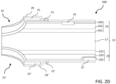
- FIG. 2A there Figure 2B , there Figure 2C and the 2D figure represent, by means of partial and schematic sectional views, successive stages of an example of a method of manufacturing a power component according to a second embodiment.
- Figures 2A to 2D illustrate the method of manufacturing a power component according to a second embodiment.
- the method of Figures 2A to 2D differs from the process of Figures 1A to 1E essentially in that, in the process of Figures 2A to 2D , the electrically insulating layer 29 is formed after the glass layer 31.
- FIG. 2A illustrates a structure obtained at the end of a step of forming the glass layers 31 and 31' respectively on the upper and lower faces of the structure illustrated in Figure 1A .
- the step of forming the glass layers 31 and 31' illustrated in Figure 2A is for example similar to the step of forming the glass layers 31 and 31' illustrated in Figure 1C except that, in Figure 2A , the glass layers 31 and 31' are respectively formed on and in contact with the SIPOS layers 21 and 21'.
- the layer 31 is thus formed locally on the surface of the layer 21 and for example in contact with it.
- the layer 31 thus covers the layer 21 located in the bottom and on the sides of the groove 15 and on the surface of the groove 15 without extending over the entire surface of the layer 21 on the surface of the groove 15.
- the layer 31' is formed locally on the surface of the layer 21' and for example in contact with it.
- the layer 31' thus covers the layer 21' located in the bottom and on the sides of the groove 15' and on the surface of the groove 15' without extending over the entire surface of the layer 21' on the surface of the groove 15'.
- FIG. 2B illustrates a structure obtained at the end of a step of forming the electrically insulating layers 29 and 29' respectively on the upper and lower faces of the structure illustrated in Figure 2A .
- the step of forming the electrically insulating layers 29 and 29' illustrated in Figure 2B is for example similar to the step of forming the electrically insulating layers 29 and 29' illustrated in Figure 1B except that, in Figure 2B , the electrically insulating layer 29 is formed on and in contact with the glass layer 31 and with the portion of the SIPOS layer 21 not covered by the glass layer 31. Furthermore, the step of forming the electrically insulating layers 29 and 29' illustrated in Figure 2B differs from the step of forming the electrically insulating layers 29 and 29' illustrated in Figure 1B in that, in Figure 2B , the electrically insulating layer 29' is formed on and in contact with the glass layer 31' and with the portion of the SIPOS layer 21' not covered by the glass layer 31'.
- the layer 29 thus covers the upper face of the glass layer 31 located on the sides and in the bottom of the groove 15 and extending to the surface of the groove 15 and further covers the part of the upper face of the layer 21 on the surface of the groove 15 not covered by the layer 31.
- the layer 29 covers the side of the glass layer 31 on the surface of the groove 15.
- the glass layer 31 is in contact, by its lower face, with the upper face of the SIPOS layer 21 and, by its upper face, with the lower face of the layer 29.
- the layer 29' thus covers the lower face of the glass layer 31' located on the sides and in the bottom of the groove 15' and extending to the surface of the groove 15' and further covers the portion of the lower face of the layer 21' on the surface of the groove 15' not covered by the glass layer 31'.
- the layer 29' covers the side of the glass layer 31' on the surface of the groove 31'.
- the glass layer 31' is in contact, by its upper face, with the lower face of the SIPOS layer 21' and, by its lower face, with the upper face of the layer 29'.
- FIG. 2C illustrates a structure obtained at the end of a step of structuring or localized removal of layers 21 and 29 and layers 21' and 29' of the structure illustrated in Figure 2B .
- the structuring step of layers 21 and 29 and layers 21' and 29' illustrated in Figure 2C is for example similar to the step of structuring layers 21 and 29 and layers 21' and 29' illustrated in Figure 1D except that, in Figure 2C , the masking layers for etching layers 21 and 29 and layers 21' and 29' are formed respectively on and in contact with the upper face of layer 29 and on and in contact with the lower face of layer 29'.
- FIG. 2D figure illustrates a structure obtained at the end of a step of forming electrically conductive layers 33 and 33' respectively on the upper and lower faces of the structure illustrated in Figure 2C .
- the formation step of layers 33 and 33' illustrated in 2D figure is for example identical to the step of forming layers 33 and 33' illustrated in Figure 1E .
- An advantage of the embodiments described is that they make it possible to avoid one or more photolithography steps and therefore reduce the costs of manufacturing of the electronic component considered.
- the localized deposition of the glass layers 31, 31' makes it possible to avoid a localized etching step of said glass layers.
- the step of localized removal of the passivation layers 21, 29 and, where appropriate, 21', 29' is implemented after the deposition of the glass 31, 31' in the grooves 15, 15'.
- the grooves 15, 15' are at least partially filled by the glass 31, 31'.
- a reduced thickness of photosensitive masking resin can be used for the step of localized etching of the layers 21, 29 and 21', 29'. This makes it possible to simplify this localized etching step and to reduce its cost.
- the present invention can be applied to any device comprising a peripheral mesa groove passivated with a glass layer and a SIPOS layer.
Landscapes
- Electrodes Of Semiconductors (AREA)
- Thyristors (AREA)
- Semiconductor Integrated Circuits (AREA)
- Formation Of Insulating Films (AREA)
Abstract
La présente description concerne un procédé de formation d'un composant électronique de puissance (100) dans et sur un substrat semiconducteur (13), comportant les étapes successives suivantes :
a) formation d'un sillon périphérique (15) dans le substrat semiconducteur du côté d'une première face du substrat semiconducteur ;
b) dépôt d'une couche en polysilicium dopé en oxygène (21), sur et en contact avec le fond et les parois du sillon périphérique et avec ladite première face du substrat semiconducteur ;
c) dépôt localisé d'une couche en verre (31), sur la couche en polysilicium dopé en oxygène (21), la couche en verre (31) s'étendant dans le sillon périphérique (15) et se prolongeant sur une partie de ladite première face du substrat semiconducteur ; et
d) gravure de la couche en polysilicium dopé en oxygène (21) de sorte qu'elle s'étende sur ladite première face du substrat semiconducteur au-delà de la couche en verre (31).
a) formation d'un sillon périphérique (15) dans le substrat semiconducteur du côté d'une première face du substrat semiconducteur ;
b) dépôt d'une couche en polysilicium dopé en oxygène (21), sur et en contact avec le fond et les parois du sillon périphérique et avec ladite première face du substrat semiconducteur ;
c) dépôt localisé d'une couche en verre (31), sur la couche en polysilicium dopé en oxygène (21), la couche en verre (31) s'étendant dans le sillon périphérique (15) et se prolongeant sur une partie de ladite première face du substrat semiconducteur ; et
d) gravure de la couche en polysilicium dopé en oxygène (21) de sorte qu'elle s'étende sur ladite première face du substrat semiconducteur au-delà de la couche en verre (31).
Description
- La présente description concerne de façon générale les composants électroniques semi-conducteurs et plus particulièrement les composants électroniques de puissance comme les thyristors et triacs.
- On connaît différentes technologies de composants de puissance et différentes techniques de fabrication de ces composants. On connaît notamment la technologie MESA qui consiste à entourer une jonction PN, formée dans toute la surface du composant, d'un sillon (aussi appelé tranchée) rempli de verre sur au moins une face du composant comme terminaison de la jonction.
- Il existe un besoin d'amélioration des composants électroniques de puissance, notamment les composants électroniques de la technologie MESA, et de leurs techniques de fabrication. Plus particulièrement, il existe un besoin de stabiliser des courants de fuite et/ou d'augmentation de la tenue en tension dans ces composants.
- Pour cela, un mode de réalisation prévoit un procédé de formation d'un composant électronique de puissance dans et sur un substrat semiconducteur, comportant les étapes successives suivantes :
- a) formation d'un sillon périphérique dans le substrat semiconducteur du côté d'une première face du substrat semiconducteur ;
- b) dépôt d'une couche en polysilicium dopé en oxygène, sur et en contact avec le fond et les parois du sillon périphérique et avec ladite première face du substrat semiconducteur ;
- c) dépôt localisé d'une couche en verre, sur la couche en polysilicium dopé en oxygène, la couche en verre s'étendant dans le sillon périphérique et se prolongeant sur une partie de ladite première face du substrat semiconducteur ; et
- d) gravure de la couche en polysilicium dopé en oxygène de sorte qu'elle s'étende sur ladite première face du substrat semiconducteur au-delà de la couche en verre.
- Selon un mode de réalisation, le procédé comporte, entre les étapes b) et c), une étape e) de dépôt d'une couche électriquement isolante sur et en contact avec la couche en polysilicium dopé en oxygène.
- Selon un mode de réalisation, le procédé comporte, entre les étapes c) et d), une étape e) de dépôt d'une couche électriquement isolante sur et en contact avec la couche de verre et une partie de la couche en polysilicium dopé en oxygène non recouverte par la couche en verre.
- Selon un mode de réalisation, la couche électriquement isolante est gravée, en même temps que la couche en polysilicium dopé en oxygène lors de l'étape d).
- Selon un mode de réalisation, le dépôt de la couche en verre lors de l'étape c) est effectué par sérigraphie.
- Selon un mode de réalisation, le sillon a une profondeur supérieure à 75 µm.
- Selon un mode de réalisation, la couche en polysilicium dopé en oxygène a une épaisseur comprise entre 0,1 µm et 2 µm.
- Un autre mode de réalisation prévoit un composant comportant :
- un sillon périphérique formée dans un substrat semiconducteur du côté d'une première face du substrat semiconducteur ;
- une couche en polysilicium dopé en oxygène, formée sur et en contact avec le fond et les parois du sillon périphérique et avec ladite première face du substrat semiconducteur ; et
- une couche en verre, formée sur la couche en polysilicium dopé en oxygène, la couche en verre s'étendant dans le sillon périphérique et se prolongeant sur une partie de ladite première face du substrat semiconducteur et la couche en polysilicium dopé en oxygène s'étendant sur ladite première face du substrat semiconducteur au-delà de la couche en verre.
- Selon un mode de réalisation, le composant comporte une couche électriquement isolante entre la couche en polysilicium dopé en oxygène et la couche en verre, la couche électriquement isolante étant en contact, par une première face, avec la couche en polysilicium dopé en oxygène et, par une deuxième face opposée à la première face, avec la couche en verre.
- Selon un mode de réalisation, le composant comporte une couche électriquement isolante, la couche en verre étant en contact, par une première face, avec la couche électriquement isolante et, par une deuxième face opposée à la première face, avec la couche en polysilicium dopé en oxygène et la couche électriquement isolante étant en contact avec une partie de la couche en polysilicium dopé en oxygène non recouverte par la couche en verre.
- Selon un mode de réalisation, le sillon a une profondeur supérieure à 75 µm.
- Selon un mode de réalisation, la couche en polysilicium dopé en oxygène a une épaisseur comprise entre 0,1 µm et 2 µm.
- Un autre mode de réalisation prévoit un circuit de contrôle de puissance comprenant un composant électronique de puissance tel que décrit.
- Ces caractéristiques et avantages, ainsi que d'autres, seront exposés en détail dans la description suivante de modes de réalisation particuliers faite à titre non limitatif en relation avec les figures jointes parmi lesquelles :
- la
figure 1A , lafigure 1B , lafigure 1C , lafigure 1D et lafigure 1E représentent, par des vues en coupe, partielles et schématiques, des étapes successives d'un exemple d'un procédé de fabrication d'un composant de puissance selon un premier mode de réalisation ; et - la
figure 2A , lafigure 2B , lafigure 2C et lafigure 2D représentent, par des vues en coupe, partielles et schématiques, des étapes successives d'un exemple d'un procédé de fabrication d'un composant de puissance selon un deuxième mode de réalisation. - De mêmes éléments ont été désignés par de mêmes références dans les différentes figures. En particulier, les éléments structurels et/ou fonctionnels communs aux différents modes de réalisation peuvent présenter les mêmes références et peuvent disposer de propriétés structurelles, dimensionnelles et matérielles identiques.
- Par souci de clarté, seuls les étapes et éléments utiles à la compréhension des modes de réalisation décrits ont été représentés et sont détaillés. En particulier, seule la réalisation des sillons d'isolation périphériques du composant, et des couches de passivation formées dans ces sillons, participant à la diminution de courants de fuite et à l'augmentation de la tenue en tension du composant, a été détaillée.
- Sauf précision contraire, lorsque l'on fait référence à deux éléments connectés entre eux, cela signifie directement connectés sans éléments intermédiaires autres que des conducteurs, et lorsque l'on fait référence à deux éléments reliés (en anglais "coupled") entre eux, cela signifie que ces deux éléments peuvent être connectés ou être reliés par l'intermédiaire d'un ou plusieurs autres éléments.
- Dans la description qui suit, lorsque l'on fait référence à des qualificatifs de position absolue, tels que les termes "avant", "arrière", "haut", "bas", "gauche", "droite", etc., ou relative, tels que les termes "dessus", "dessous", "supérieur", "inférieur", etc., ou à des qualificatifs d'orientation, tels que les termes "horizontal", "vertical", etc., il est fait référence sauf précision contraire à l'orientation des figures.
- Sauf précision contraire, les expressions "environ", "approximativement", "sensiblement", et "de l'ordre de" signifient à 10 % près, de préférence à 5 % près.
- Les composants électroniques de puissance dits verticaux comportent généralement un substrat semiconducteur comportant au moins une jonction PN planaire horizontale entourée latéralement par un sillon périphérique s'étendant verticalement dans le substrat. Afin de limiter les fuites de courant et/ou d'augmenter la tenue en tension, les composants électroniques de puissance verticaux doivent comporter une structure de passivation recouvrant les flancs et le fond du sillon et une partie d'une face du substrat semiconducteur, à la surface du sillon. La structure de passivation peut par exemple comporter une couche en polysilicium dopé en oxygène ou SIPOS (de l'anglais "Semi-Insulating Polycrystalline Silicon"). La structure de passivation peut, en outre, comporter une couche en verre formée sur la couche en SIPOS et plus précisément formée dans le sillon et sur ladite face du substrat semiconducteur, à la surface du sillon, de sorte qu'elle recouvre entièrement la couche en SIPOS.
- Dans les composants électroniques de puissance, la profondeur du sillon engendre une complexité dans la gravure de la couche en SIPOS qui est réalisée avant la formation de la couche en verre. Plus particulièrement elle engendre une complexité dans la formation de la résine de masquage à travers de laquelle la couche en SIPOS est gravée, notamment sa structuration par photolithographie. En effet, le dépôt de la résine de masquage n'est pas uniforme et une quantité importante de résine doit être déposée afin que le sommet du sillon soit recouvert par la résine. Dans certains cas, l'épaisseur de résine sur la face supérieure du substrat est telle qu'une unique étape de photolithographie ne permet pas de l'insoler localement dans toute son épaisseur. Par exemple, dans le cas de composants électroniques de puissance à très haute tenue en tension (par exemple supérieure ou égale à 1200 V), la profondeur du sillon peut être supérieure à une centaine de micromètres et l'épaisseur de la résine de masquage peut atteindre plusieurs dizaines de micromètres. Ainsi, plusieurs cycles de dépôt puis insolation de la résine peuvent être nécessaires pour obtenir l'épaisseur souhaitée. Il en résulte une complexité accrue et une augmentation du coût de la fabrication des composants.
- Les composant électronique de puissance décrits peuvent par exemple, être utilisés dans divers circuit de contrôle, de conversion ou d'adaptation de puissance, par exemple dans des équipements industriels, des dispositifs d'affichage ou d'éclairage, des équipements de télécommunications, des équipements électroménagers, des dispositifs automobiles, etc.
- La
figure 1A , lafigure 1B , lafigure 1C , lafigure 1D et lafigure 1E représentent, par des vues en coupe, partielles et schématiques, des étapes successives d'un exemple d'un procédé de fabrication d'un composant de puissance selon un premier mode de réalisation. Lesfigures 1A à 1E illustrent plus particulièrement un exemple d'un procédé de formation d'une structure périphérique de passivation d'un composant de puissance selon le premier mode de réalisation. On notera que sur les figures, la réalisation d'un unique composant est représentée. En pratique, une pluralité de composants peuvent être formés simultanément dans et sur un même substrat semiconducteur, le substrat étant ensuite découpé en puces individuelles comportant chacune un unique composant électronique de puissance. - La
figure 1A représente une structure de départ comportant un substrat 13 semiconducteur dans lequel est formé, du côté de sa face supérieure, un sillon périphérique 15 entourant latéralement une jonction PN planaire horizontale du composant. Enfigure 1A seulement une partie de la structure de départ a été représentée. En pratique la structure s'étend au-delà du bord droit représenté en pointillés enfigure 1A , le sillon périphérique 15 entourant la structure. - Le composant a par exemple, en vue de dessus, une forme générale carrée ou rectangulaire, par exemple à coins arrondis, ou circulaire. Le substrat 13 est, par exemple, en silicium.
- A titre d'exemple, le substrat 13 comprend une partie centrale 17, par exemple dopée d'un premier type de conductivité, par exemple dopée de type N. A titre d'exemple, le substrat 13 comprend, de plus, une partie supérieure 19, par exemple dopée d'un deuxième type de conductivité différent du premier type de conductivité, par exemple dopée de type P. A titre d'exemple, la partie supérieure 19 est en contact, par sa face inférieure avec la face supérieure de la partie centrale 17 du substrat 13.
- La partie supérieure 19 du substrat 13 comprend par exemple un gradient de dopage croissant à partir de sa face inférieure. De plus, la partie supérieure 19 du substrat 13 comprend par exemple plusieurs éléments dopants différents.
- A titre d'exemple, la partie supérieure 19 du substrat 13 comprend une première portion 191, en contact, par sa face inférieure avec la face supérieure de la partie 17 du substrat 13. La première portion 191 est par exemple dopée en atomes d'aluminium.
- De plus, la partie supérieure 19 du substrat 13 comprend par exemple une deuxième portion 193, en contact, par sa face inférieure avec la face supérieure de la portion 191. La deuxième portion 193 est par exemple dopée en atomes de gallium.
- A titre d'exemple, la partie supérieure 19 du substrat 13 comprend, en outre, une troisième portion 195, en contact, par sa face inférieure avec la face supérieure de la portion 193. La troisième portion 195 est par exemple dopée en atomes, de gallium.
- A titre d'exemple, le sillon 15 formé sur la face supérieure de la structure de départ s'étend à partir de la face supérieure de la partie supérieure 19 du substrat 13 dans le substrat 13 et débouche dans la première partie 17 du substrat 13. Le sillon s'étend ainsi, par exemple, à travers les portions 195, 193 et 191. Ainsi, le sillon 15 traverse la jonction PN formée par le plan horizontal d'interface entre les parties supérieure 19 et centrale 17.
- La profondeur du sillon 15 à partir de la face supérieure du substrat 13 est par exemple supérieure à 30 µm, par exemple supérieure 75 µm, par exemple supérieure à 105 µm, par exemple comprise entre 105 µm et 150 µm.
- La structure de la
figure 1A comporte, de plus, une couche 21 en polysilicium dopé en oxygène ou SIPOS (de l'anglais "Semi-Insulating Polycrystalline Silicon"), s'étendant sur les parois des sillons 15 et sur et en contact avec la face supérieure du substrat 13, à la surface des sillons 15. A titre d'exemple, la couche en SIPOS 21 a un pourcentage en oxygène compris entre 10 % et 50 %, par exemple compris entre 20 % et 40 %. - La couche en SIPOS 21 est, par exemple déposée à la surface du substrat 13 et dans les sillons 15 par un procédé de dépôt chimique en phase vapeur, par exemple par un procédé de dépôt chimique en phase vapeur à basse pression ou LPCVD (de l'anglais " Low pressure chemical vapor deposition"). A titre d'exemple, la couche en SIPOS 21 a une épaisseur comprise entre 0,1 µm et 2 µm, par exemple comprise entre 0,1 µm et 1 µm, par exemple de l'ordre de 0,5 µm.
- La structure de départ illustrée en
figure 1A est par exemple symétrique horizontalement. Le substrat 13 comporte par exemple une partie inférieure 23 comportant des portions 231, 233 et 235 par exemple respectivement similaires aux portions 191, 193 et 195 de la partie supérieure 19. La structure comporte par exemple un sillon 15' formé à partir de la face inférieure du substrat 13. A titre d'exemple, le sillon 15' s'étend dans la partie inférieure 23 et débouche dans la partie centrale 17 du substrat 13. La structure de départ comporte par exemple une autre couche en SIPOS 21' s'étendant sur et en contact avec la face inférieure du substrat 13 et sur les parois du sillon 15' formé à partir de la face inférieure du substrat 13. Ainsi, le sillon 15' traverse la jonction PN formée par le plan horizontal d'interface entre les parties inférieure 23 et centrale 17 du substrat. - La structure de départ comporte de plus une zone dopée localisée 25 du coté de la face supérieure du substrat 13, affleurant cette même face. La structure peut en outre comporter une zone dopée localisée 27 du coté de la face inférieure du substrat 13, affleurant cette même face.
- A titre d'exemple, les couches 17, 19 et 23 s'étendent chacune sur toute la surface du substrat. Les zones 25 et 27 sont quant à elles localisées respectivement sur une partie seulement de la surface du substrat.
- Les zones 25 et 27 sont, par exemple, dopées du premier type de conductivité, par exemple du type N. A titre d'exemple, les zones 25 et 27 sont plus fortement dopées que la partie centrale 17 du substrat 13 et que les portions 195 et 235 du substrat 13. A titre d'exemple les zones 25 et 27 sont dopées d'atomes de phosphore.
- La structure de départ est ainsi constituée d'un premier empilement vertical de quatre régions 19, 17, 23, et 27 alternativement dopées P et N, et d'un deuxième empilement vertical de quatre régions 25, 19, 17 et 23 alternativement dopées N et P, qui définissent un triac. Les modes de réalisation décrits ne se limitent pas à cet exemple de composant. A titre d'exemple, la région 27 peut être omise dans le cas d'une structure de type thyristor. Plus généralement, les modes de réalisation décrits peuvent être appliqués à tout composant électronique de puissance dit vertical, comportant une jonction PN horizontal et une structure de passivation formée dans un sillon d'isolation périphérique traversant verticalement la jonction PN.
- La
figure 1B illustre une structure obtenue à l'issue d'une étape de formation d'une couche électriquement isolante 29 sur la face supérieure de la structure illustrée enfigure 1A . Dans cet exemple, une couche électriquement isolante 29' est en outre formée sur la face inférieure de la structure. - Plus particulièrement, lors de cette étape, la couche 29 est formée pleine plaque, c'est-à-dire qu'elle est formée sur l'ensemble de la face supérieure de la structure illustrée en
figure 1A . Lors de cette étape, la couche 29 est formée en contact avec la couche en SIPOS 21. La couche 29 recouvre par exemple la face supérieure de la couche 21 située sur les flancs et dans le fond du sillon 15 et s'étendant à la surface du sillon 15. - Similairement, la couche 29' est formée pleine plaque, c'est-à-dire qu'elle est formée sur l'ensemble de la face inférieure de la structure illustrée en
figure 1A . Lors de cette étape, la couche 29' est formée en contact avec la couche en SIPOS 21'. La couche 29' recouvre par exemple la face inférieure de la couche 21' située sur les flancs et dans le fond du sillon 15' et s'étendant à la surface du sillon 15'. - A titre d'exemple, les couches 29 et 29' sont en verre non dopé, par exemple en verre de silicium non dopé (USG, de l'anglais "Undoped Silicon Glass") ou en verre phosphosilicate non dopé (PSG, de l'anglais " PhosphoSilicate Glass"). Les couches 29 et 29' sont par exemple déposées par un procédé de dépôt chimique en phase vapeur, par exemple par un procédé de dépôt LPCVD. A titre d'exemple les couches 29 et 29' ont une épaisseur comprise entre 0,1 µm et 1,5 µm, par exemple comprise entre 0,5 µm et 1 µm.
- La
figure 1C illustre une structure obtenue à l'issue d'une étape de formation d'une couche en verre 31 sur la face supérieure de la structure illustrée enfigure 1B . Dans cet exemple, une couche en verre 31' est en outre formée sur la face inférieure de la structure. - Plus particulièrement, lors de cette étape, la couche 31 est formée localement à la surface de la couche 29 et, par exemple, en contact avec celle-ci. La couche 31 recouvre ainsi la couche 29 située dans le fond et sur les flancs du sillon 15 et à la surface du sillon 15 sans s'étendre sur toute la surface de la couche 29 à la surface de la sillon 15.
- Similairement, lors de cette étape, la couche 31' est formée localement à la surface de la couche 29' et, par exemple, en contact avec celle-ci. La couche 31' recouvre ainsi la couche 29' située dans le fond et sur les flancs du sillon 15' et à la surface du sillon 15' sans s'étendre sur toute la surface de la couche 29' à la surface du sillon 15'.
- Les couches 31 et 31' sont déposées par un procédé de dépôt localisé, par exemple par sérigraphie. Cette étape consiste par exemple au dépôt d'une pâte de verre à travers un masque situé à la surface de la couche 29 ou de la couche 29'. A titre d'exemple, après ce dépôt, les couches 31 et 31' subissent une ou des étapes de recuit. L'étape de recuit peut par exemple comprendre une étape de pyrolyse à une température comprise entre 300 °C et 700 °C, par exemple de l'ordre de 500 °C. L'étape de recuit peut en outre comprendre une étape de frittage à une température comprise entre 500 °C et 1000 °C, par exemple de l'ordre de 800 °C.
- A titre d'exemple, les couches 31 et 31' ont une épaisseur non constante sur l'ensemble de leurs surfaces. Elle est par exemple plus importante au fond des sillons 15 et 15' (c'est-à-dire dans les sillons de la plaquette entre les composants) qu'en leur sommet et à la surface des sillons 15 et 15'.
- L'épaisseur des couches 31 et 31' à la surface du substrat 13 en périphérie des sillons 15 et 15' est par exemple comprise entre 10 µm et 40 µm, par exemple comprise entre 20 µm et 30 µm.
- L'épaisseur des couches 31 et 31' dans le fond des sillons 15 et 15' est par exemple comprise entre 20 µm et 70 µm, par exemple comprise entre 40 µm et 50 µm.
- La
figure 1D illustre une structure obtenue à l'issue d'une étape de retrait localisé des couches 21 et 29 et des couches 21' et 29' de la structure illustrée enfigure 1C . - Lors de cette étape, on vient par exemple dans un premier temps former par photolithographie une couche de masquage (non représentée) en une résine photosensible sur la face supérieure de la structure illustrée en
figure 1C . - A titre d'exemple, la résine photosensible de la couche de masquage est déposée par centrifugation (spin-coating), exposée aux UV puis développée dans un solvant. A titre d'exemple, la couche de masquage recouvre toute la surface de la couche en verre 31 . La couche de masquage se prolonge en outre latéralement au delà la couche en verre 31, et recouvre ainsi une partie des couches 21 et 29 au voisinage de la couche en verre 31. La couche de masquage ne recouvre toutefois pas les couches 21 et 29 en vis-à-vis d'une partie centrale du composant.
- Lors de cette étape, et dans un second temps, on vient graver les couches 21 et 29 à travers la couche de masquage. A titre d'exemple la gravure des couches 21 et 29 est une gravure humide.
- Similairement, on vient par exemple également lors de cette étape former par photolithographie une couche de masquage (non représentée) en une résine photosensible sur la face inférieure de la structure illustrée en
figure 1C puis graver les couches 21' et 29' à travers la couche de masquage. - A l'issue de cette étape, les couches 21 et 29 s'étendent, par exemple, dans le fond et sur les flancs des sillons 15 et à la surface du sillon 15 sur une partie de la face supérieure du substrat 13. A titre d'exemple, les couches 21 et 29 s'étendent sur la face supérieure du substrat 13 au-delà de la couche en verre 31, c'est-à-dire que les couches 21 et 29 s'étendent sur le substrat 13 dans l'ensemble du vis-à-vis de la couche en verre 31 et se prolonge sur une partie du substrat 13 en dehors du vis-à-vis de la couche en verre 31. A titre d'exemple, à l'issue de cette étape, les couches 21 et 29 ne recouvrent pas la zone 25.
- Similairement, les couches 21' et 29' s'étendent, par exemple, dans le fond et sur les flancs des sillons 15' et à la surface du sillon 15' sur une partie de la face inférieure du substrat 13. A titre d'exemple, les couches 21' et 29' s'étendent sur la face inférieure du substrat 13 au delà de la couche en verre 31', c'est-à-dire que les couches 21' et 29' s'étendent sur le substrat 13 dans l'ensemble du vis-à-vis de la couche en verre 31' et se prolonge sur une partie du substrat 13 en dehors du vis-à-vis de la couche en verre 31'. A titre d'exemple, à l'issue de cette étape, les couches 21' et 29' ne recouvrent pas la zone 27.
- La
figure 1E illustre une structure obtenue à l'issue d'une étape de formation de couches électriquement conductrices 33 et 33' respectivement sur les faces supérieure et inférieure de la structure illustrée enfigure 1D . - Plus particulièrement, lors de cette étape, on vient par exemple former une couche électriquement conductrice 33 dans le prolongement des couches 21 et 29 à la surface du substrat 13. A titre d'exemple, la couche 33 est formée en contact avec une partie de la face supérieure du substrat 13 non recouverte par les couches 21 et 29. A titre d'exemple, la couche 33 s'étend à partir des couches 21 et 29 et est, par exemple, en contact par son flanc avec le flanc des couches 21 et 29.
- Similairement, lors de cette étape, on vient également par exemple former une couche électriquement conductrice 33' dans le prolongement des couches 21' et 29' à la surface du substrat 13. A titre d'exemple, la couche 33' est formée en contact avec une partie de la face inférieure du substrat 13 non recouverte par les couches 21' et 29'. A titre d'exemple, la couche 33' s'étend à partir des couches 21' et 29' et est, par exemple, en contact par son flanc avec le flanc des couches 21' et 29'.
- A titre d'exemple les couches 33 et 33' sont en un matériau métallique, par exemple en or et/ou en nickel. A titre d'exemple, les couches 33 et 33' sont formées par dépôt par voie humide, par exemple par un dépôt chimique dit sans électrodes (en anglais "electroless").
- Lors de cette étape, le dépôt est formé uniquement sur les parties conductrices de la structure et n'est pas formé sur les parties isolantes de la structure. Les couches 33 et 33' sont ainsi formées sélectivement en contact avec les parties semiconductrices libres de la structure illustrée en
figure 1D . Les couches 33 et 33' sont alors formées respectivement en contact avec la face supérieure et la face inférieure du substrat 13. A titre d'exemple, les couches 29 et 29' permettent, lors de cette étape, de protéger respectivement la face supérieure de la couche 21 et la face inférieure de la couche 21' du dépôt des couches 33 et 33'. Les couches 29 et 29' permettent notamment de protéger respectivement les couches 21 et 21' du dépôt des couches 33 et 33'. En effet, en l'absence des couches 29 et 29', les couches 33 et 33' auraient tendance à se former en outre sur une partie des couches 21 et 21' qui sont semi-isolantes. - La
figure 2A , lafigure 2B , lafigure 2C et lafigure 2D représentent, par des vues en coupe, partielles et schématiques, des étapes successives d'un exemple d'un procédé de fabrication d'un composant de puissance selon un deuxième mode de réalisation. - Plus particulièrement, les
figures 2A à 2D illustrent le procédé de fabrication d'un composant de puissance selon un deuxième mode de réalisation. Le procédé desfigures 2A à 2D diffère du procédé desfigures 1A à 1E essentiellement en ce que, dans le procédé desfigures 2A à 2D , la couche électriquement isolante 29 est formée après la couche en verre 31. - La
figure 2A illustre une structure obtenue à l'issue d'une étape de formation des couches en verre 31 et 31' respectivement sur les faces supérieure et inférieure de la structure illustrée enfigure 1A . - L'étape de formation des couches en verre 31 et 31' illustrée en
figure 2A est par exemple similaire à l'étape de formation des couches en verre 31 et 31' illustrée enfigure 1C à la différence près que, enfigure 2A , les couches en verre 31 et 31' sont respectivement formées sur et en contact avec les couches en SIPOS 21 et 21'. - Lors de cette étape, la couche 31 est ainsi formée localement à la surface de la couche 21 et par exemple en contact avec celle-ci. La couche 31 recouvre ainsi la couche 21 située dans le fond et sur les flancs du sillon 15 et à la surface du sillon 15 sans s'étendre sur toute la surface de la couche 21 à la surface du sillon 15.
- Similairement, lors de cette étape, la couche 31' est formée localement à la surface de la couche 21' et par exemple en contact avec celle-ci. La couche 31' recouvre ainsi la couche 21' située dans le fond et sur les flancs du sillon 15' et à la surface du sillon 15' sans s'étendre sur toute la surface de la couche 21' à la surface du sillon 15'.
- La
figure 2B illustre une structure obtenue à l'issue d'une étape de formation des couches électriquement isolantes 29 et 29' respectivement sur les faces supérieure et inférieure de la structure illustrée enfigure 2A . - L'étape de formation des couches électriquement isolantes 29 et 29' illustrée en
figure 2B est par exemple similaire à l'étape de formation des couches électriquement isolantes 29 et 29' illustrée enfigure 1B à la différence près que, enfigure 2B , la couche électriquement isolante 29 est formée sur et en contact avec la couche en verre 31 et avec la partie de la couche en SIPOS 21 non recouverte par la couche en verre 31. En outre, l'étape de formation des couches électriquement isolantes 29 et 29' illustrée enfigure 2B diffère de l'étape de formation des couches électriquement isolantes 29 et 29' illustrée enfigure 1B en ce que, enfigure 2B , la couche électriquement isolante 29' est formée sur et en contact avec la couche en verre 31' et avec la partie de la couche en SIPOS 21' non recouverte par la couche en verre 31'. - La couche 29 recouvre ainsi la face supérieure de la couche en verre 31 située sur les flancs et dans le fond du sillon 15 et s'étendant à la surface du sillon 15 et recouvre en outre la partie de la face supérieure de la couche 21 à la surface du sillon 15 non recouverte par la couche 31. A titre d'exemple, la couche 29 recouvre le flanc de la couche en verre 31 à la surface du sillon 15. A titre d'exemple, à l'issue de cette étape, la couche en verre 31 est en contact, par sa face inférieure, avec la face supérieure de la couche en SIPOS 21 et, par sa face supérieure, avec la face inférieure de la couche 29.
- Similairement, la couche 29' recouvre ainsi la face inférieure de la couche en verre 31' située sur les flancs et dans le fond du sillon 15' et s'étendant à la surface du sillon 15' et recouvre en outre la partie de la face inférieure de la couche 21' à la surface du sillon 15' non recouverte par la couche en verre 31'. A titre d'exemple, la couche 29' recouvre le flanc de la couche en verre 31' à la surface du sillon 31'. A titre d'exemple, à l'issue de cette étape, la couche en verre 31' est en contact, par sa face supérieure, avec la face inférieure de la couche en SIPOS 21' et, par sa face inférieure, avec la face supérieure de la couche 29'.
- La
figure 2C illustre une structure obtenue à l'issue d'une étape de structuration ou retrait localisé des couches 21 et 29 et des couches 21' et 29' de la structure illustrée enfigure 2B . - L'étape de structuration des couches 21 et 29 et des couches 21' et 29' illustrée en
figure 2C est par exemple similaire à l'étape de structuration des couches 21 et 29 et des couches 21' et 29' illustrée enfigure 1D à la différence près que, enfigure 2C , les couche de masquage permettant de graver les couches 21 et 29 et les couches 21' et 29' sont formées respectivement sur et en contact avec la face supérieure de la couche 29 et sur et en contact avec la face inférieure de la couche 29'. - La
figure 2D illustre une structure obtenue à l'issue d'une étape de formation de couches électriquement conductrices 33 et 33' respectivement sur les faces supérieure et inférieure de la structure illustrée enfigure 2C . - L'étape de formation des couches 33 et 33' illustrée en
figure 2D est par exemple identique à l'étape de formation des couches 33 et 33' illustrée enfigure 1E . - Un avantage des modes de réalisation décrits est qu'ils permettent de s'affranchir d'une ou plusieurs étapes de photolithographie et donc de diminuer les coûts de fabrication du composant électronique considéré. En particulier, le dépôt localisé des couches de verre 31, 31', permet de s'affranchir d'une étape de gravure localisée desdites couches de verre.
- En outre, l'étape de retrait localisé des couches de passivation 21, 29 et, le cas échéant, 21', 29', est mise en oeuvre après le dépôt du verre 31, 31' dans les sillons 15, 15'. Ainsi, lors de cette étape, les sillons 15, 15' sont au moins partiellement comblées par le verre 31, 31'. Il en résulte qu'une épaisseur réduite de résine photosensible de masquage peut être utilisée pour l'étape de gravure localisée des couches 21, 29 et 21', 29'. Ceci permet de simplifier cette étape de gravure localisée et d'en réduire le coût.
- Divers modes de réalisation et variantes ont été décrits. La personne du métier comprendra que certaines caractéristiques de ces divers modes de réalisation et variantes pourraient être combinées, et d'autres variantes apparaîtront à la personne du métier. En particulier, les modes de réalisations décrits ne se limitent pas aux exemples de dimensions et de matériaux mentionnés ci-dessus.
- De plus, bien que les modes de réalisation aient été décrits pour un triac, la présente invention elle peut s'appliquer à tous dispositifs comportant un sillon périphérique mésa passivée avec une couche de verre et une couche en SIPOS.
- Enfin, la mise en oeuvre pratique des modes de réalisation et variantes décrits est à la portée de la personne du métier à partir des indications fonctionnelles données ci-dessus.
Claims (13)
- Procédé de formation d'un composant électronique de puissance (100 ; 200) dans et sur un substrat semiconducteur (13), comportant les étapes successives suivantes :a) formation d'un sillon périphérique (15, 15') dans le substrat semiconducteur (13) du côté d'une première face du substrat semiconducteur (13) ;b) dépôt d'une couche en polysilicium dopé en oxygène (21, 21'), sur et en contact avec le fond et les parois du sillon périphérique (15, 15') et avec ladite première face du substrat semiconducteur (13) ;c) dépôt localisé d'une couche en verre (31, 31'), sur la couche en polysilicium dopé en oxygène (21, 21'), la couche en verre (31, 31') s'étendant dans le sillon périphérique (15, 15') et se prolongeant sur une partie de ladite première face du substrat semiconducteur (13) ; etd) gravure de la couche en polysilicium dopé en oxygène (21, 21') de sorte qu'elle s'étende sur ladite première face du substrat semiconducteur (13) au-delà de la couche en verre (31, 31').
- Procédé de formation d'un composant électronique de puissance selon la revendication 1, comportant, entre les étapes b) et c), une étape e) de dépôt d'une couche électriquement isolante (29, 29') sur et en contact avec la couche en polysilicium dopé en oxygène (21, 21').
- Procédé de formation d'un composant électronique de puissance selon la revendication 1, comportant, entre les étapes c) et d), une étape e) de dépôt d'une couche électriquement isolante (29, 29') sur et en contact avec la couche de verre (31, 31') et une partie de la couche en polysilicium dopé en oxygène (21, 21') non recouverte par la couche en verre (31, 31').
- Procédé de formation d'un composant électronique de puissance selon la revendication 2 ou 3, dans lequel la couche électriquement isolante (29, 29') est gravée, en même temps que la couche en polysilicium dopé en oxygène (21, 21') lors de l'étape d).
- Procédé de formation d'un composant électronique de puissance selon l'une quelconque des revendications 1 à 4, dans lequel, le dépôt de la couche en verre (31, 31') lors de l'étape c) est effectué par sérigraphie.
- Procédé de formation d'un composant électronique de puissance selon l'une quelconque des revendications 1 à 5, dans lequel le sillon (15, 15') a une profondeur supérieure à 75 µm.
- Procédé de formation d'un composant électronique de puissance selon l'une quelconque des revendications 1 à 6, dans lequel la couche en polysilicium dopé en oxygène (21, 21') a une épaisseur comprise entre 0,1 µm et 2 µm.
- Composant électronique de puissance (100 ; 200), comportant :- un sillon périphérique (15, 15') formée dans un substrat semiconducteur (13) du côté d'une première face du substrat semiconducteur (13) ;- une couche en polysilicium dopé en oxygène (21, 21'), formée sur et en contact avec le fond et les parois du sillon périphérique (15, 15') et avec ladite première face du substrat semiconducteur (13) ; et- une couche en verre (31, 31'), formée sur la couche en polysilicium dopé en oxygène (21, 21'), la couche en verre (31, 31') s'étendant dans le sillon périphérique (15, 15') et se prolongeant sur une partie de ladite première face du substrat semiconducteur (13) et la couche en polysilicium dopé en oxygène (31, 31') s'étendant sur ladite première face du substrat semiconducteur (13) au-delà de la couche en verre.
- Composant électronique de puissance (100 ; 200) selon la revendication 8, comportant une couche électriquement isolante (29, 29') entre la couche en polysilicium dopé en oxygène (21, 21') et la couche en verre (31, 31'), la couche électriquement isolante (29, 29') étant en contact, par une première face, avec la couche en polysilicium dopé en oxygène (21, 21') et, par une deuxième face opposée à la première face, avec la couche en verre (31, 31').
- Composant électronique de puissance (100 ; 200) selon la revendication 8, comportant une couche électriquement isolante (29, 29'), la couche en verre étant en contact, par une première face, avec la couche électriquement isolante (29, 29') et, par une deuxième face opposée à la première face, avec la couche en polysilicium dopé en oxygène (21, 21') et la couche électriquement isolante (29, 29') étant en contact avec une partie de la couche en polysilicium dopé en oxygène (21, 21') non recouverte par la couche en verre (31, 31').
- Composant électronique de puissance (100 ; 200) selon l'une quelconque des revendications 8 à 10, dans lequel le sillon (15, 15') a une profondeur supérieure à 75 µm.
- Composant électronique de puissance (100 ; 200) selon l'une quelconque des revendications 8 à 11, dans lequel la couche en polysilicium dopé en oxygène (21, 21') a une épaisseur comprise entre 0,1 µm et 2 µm.
- Circuit de contrôle de puissance comprenant un composant électronique de puissance selon l'une quelconque des revendications 8 à 12.
Applications Claiming Priority (1)
| Application Number | Priority Date | Filing Date | Title |
|---|---|---|---|
| FR2301163A FR3145646A1 (fr) | 2023-02-08 | 2023-02-08 | Formation d'un composant électronique de puissance |
Publications (1)
| Publication Number | Publication Date |
|---|---|
| EP4415037A1 true EP4415037A1 (fr) | 2024-08-14 |
Family
ID=86332104
Family Applications (1)
| Application Number | Title | Priority Date | Filing Date |
|---|---|---|---|
| EP24155576.2A Withdrawn EP4415037A1 (fr) | 2023-02-08 | 2024-02-02 | Formation d'un composant electronique de puissance |
Country Status (4)
| Country | Link |
|---|---|
| US (1) | US20240266423A1 (fr) |
| EP (1) | EP4415037A1 (fr) |
| CN (2) | CN118471806A (fr) |
| FR (1) | FR3145646A1 (fr) |
Citations (4)
| Publication number | Priority date | Publication date | Assignee | Title |
|---|---|---|---|---|
| US4194934A (en) * | 1977-05-23 | 1980-03-25 | Varo Semiconductor, Inc. | Method of passivating a semiconductor device utilizing dual polycrystalline layers |
| CN101794740A (zh) * | 2010-02-25 | 2010-08-04 | 海湾电子(山东)有限公司 | 抗高温整流芯片 |
| FR2990561A1 (fr) * | 2012-05-08 | 2013-11-15 | Shindengen Electric Mfg | Procede de fabrication de dispositif semi-conducteur et dispositif semi-conducteur; |
| EP3349239A1 (fr) * | 2016-11-25 | 2018-07-18 | Shindengen Electric Manufacturing Co., Ltd. | Procédé de production de dispositif à semiconducteur, et dispositif à semiconducteur |
-
2023
- 2023-02-08 FR FR2301163A patent/FR3145646A1/fr active Pending
-
2024
- 2024-01-23 US US18/420,600 patent/US20240266423A1/en active Pending
- 2024-02-02 EP EP24155576.2A patent/EP4415037A1/fr not_active Withdrawn
- 2024-02-08 CN CN202410176796.XA patent/CN118471806A/zh active Pending
- 2024-02-08 CN CN202420291885.4U patent/CN222029043U/zh active Active
Patent Citations (4)
| Publication number | Priority date | Publication date | Assignee | Title |
|---|---|---|---|---|
| US4194934A (en) * | 1977-05-23 | 1980-03-25 | Varo Semiconductor, Inc. | Method of passivating a semiconductor device utilizing dual polycrystalline layers |
| CN101794740A (zh) * | 2010-02-25 | 2010-08-04 | 海湾电子(山东)有限公司 | 抗高温整流芯片 |
| FR2990561A1 (fr) * | 2012-05-08 | 2013-11-15 | Shindengen Electric Mfg | Procede de fabrication de dispositif semi-conducteur et dispositif semi-conducteur; |
| EP3349239A1 (fr) * | 2016-11-25 | 2018-07-18 | Shindengen Electric Manufacturing Co., Ltd. | Procédé de production de dispositif à semiconducteur, et dispositif à semiconducteur |
Also Published As
| Publication number | Publication date |
|---|---|
| CN222029043U (zh) | 2024-11-19 |
| CN118471806A (zh) | 2024-08-09 |
| FR3145646A1 (fr) | 2024-08-09 |
| US20240266423A1 (en) | 2024-08-08 |
Similar Documents
| Publication | Publication Date | Title |
|---|---|---|
| EP1636130B1 (fr) | Circuit integre sur puce de hautes performances | |
| CN101048875A (zh) | 太阳能电池背接触上的导电层的接触隔离方法和相应的太阳能电池 | |
| EP0461967A2 (fr) | Composant semiconducteur à jonction Schottky pour amplification hyperfréquence et circuits logiques rapides, et procédé de réalisation d'un tel composant | |
| EP0149390B1 (fr) | Transistor à effet de champ, de structure verticale submicronique, et son procédé de réalisation | |
| EP3848978B1 (fr) | Protection esd | |
| TWI390717B (zh) | 具有積體半導體電路之光二極體及其製造方法 | |
| EP0432044A1 (fr) | Perfectionnement aux transistors de puissance en matériaux III-V sur substrat silicium, et procédé de fabrication | |
| EP0503731B1 (fr) | Procédé de réalisation d'un transistor à haute mobilité électronique intégré | |
| EP1240672A1 (fr) | Fabrication de composants unipolaires | |
| FR3145646A1 (fr) | Formation d'un composant électronique de puissance | |
| FR3112421A1 (fr) | Procédé de réalisation d’une structure d’isolation | |
| FR2864345A1 (fr) | Realisation de la peripherie d'une diode schottky a tranchees mos | |
| EP4310910A1 (fr) | Dispositif electronique de protection esd | |
| EP0949667A1 (fr) | Cellule mémoire électriquement programmable | |
| EP1517377A1 (fr) | Transistor bipolaire | |
| FR2514559A1 (fr) | Dispositif a semi-conducteurs, notamment transistor planar comportant une isolation dielectrique formee par un polyimide et procede de fabrication d'un tel dispositif | |
| EP0081423B1 (fr) | Dispositif semi-conducteur à faible capacité muni de connexions externes prises au moyen de poutres, et procédé de fabrication d'un tel dispositif | |
| EP1670066A1 (fr) | Procédé de fabrication d'un circuit intégré comprenant un miroir enterré et ce circuit | |
| FR2574594A1 (fr) | Structure integree de triac a commande par diac | |
| FR3037720A1 (fr) | Composant electronique et son procede de fabrication | |
| EP0015835B1 (fr) | Dispositif semiconducteur de commutation à fréquence élevée et procédé pour sa fabrication | |
| FR2764119A1 (fr) | Transistor bipolaire a grille isolee et procede pour sa fabrication | |
| EP3586360A2 (fr) | Composant electronique muni d'un transistor et de doigts interdigites pour former au moins une partie d'un composant capacitif au sein du composant electronique | |
| FR3143199A1 (fr) | Transistor HEMT | |
| EP4565039A1 (fr) | Dispositif optoélectronique comprenant des diodes à trois électrodes et son procédé de fabrication |
Legal Events
| Date | Code | Title | Description |
|---|---|---|---|
| PUAI | Public reference made under article 153(3) epc to a published international application that has entered the european phase |
Free format text: ORIGINAL CODE: 0009012 |
|
| STAA | Information on the status of an ep patent application or granted ep patent |
Free format text: STATUS: REQUEST FOR EXAMINATION WAS MADE |
|
| 17P | Request for examination filed |
Effective date: 20240202 |
|
| AK | Designated contracting states |
Kind code of ref document: A1 Designated state(s): AL AT BE BG CH CY CZ DE DK EE ES FI FR GB GR HR HU IE IS IT LI LT LU LV MC ME MK MT NL NO PL PT RO RS SE SI SK SM TR |
|
| STAA | Information on the status of an ep patent application or granted ep patent |
Free format text: STATUS: THE APPLICATION HAS BEEN WITHDRAWN |
|
| 18W | Application withdrawn |
Effective date: 20251202 |