EP4411804A1 - Substrate for mounting semiconductor element and semiconductor device - Google Patents
Substrate for mounting semiconductor element and semiconductor device Download PDFInfo
- Publication number
- EP4411804A1 EP4411804A1 EP22876285.2A EP22876285A EP4411804A1 EP 4411804 A1 EP4411804 A1 EP 4411804A1 EP 22876285 A EP22876285 A EP 22876285A EP 4411804 A1 EP4411804 A1 EP 4411804A1
- Authority
- EP
- European Patent Office
- Prior art keywords
- substrate
- recess
- semiconductor element
- element mounting
- conductor
- Prior art date
- Legal status (The legal status is an assumption and is not a legal conclusion. Google has not performed a legal analysis and makes no representation as to the accuracy of the status listed.)
- Withdrawn
Links
Images




Classifications
-
- H—ELECTRICITY
- H10—SEMICONDUCTOR DEVICES; ELECTRIC SOLID-STATE DEVICES NOT OTHERWISE PROVIDED FOR
- H10W—GENERIC PACKAGES, INTERCONNECTIONS, CONNECTORS OR OTHER CONSTRUCTIONAL DETAILS OF DEVICES COVERED BY CLASS H10
- H10W44/00—Electrical arrangements for controlling or matching impedance
- H10W44/20—Electrical arrangements for controlling or matching impedance at high-frequency [HF] or radio frequency [RF]
-
- H—ELECTRICITY
- H05—ELECTRIC TECHNIQUES NOT OTHERWISE PROVIDED FOR
- H05K—PRINTED CIRCUITS; CASINGS OR CONSTRUCTIONAL DETAILS OF ELECTRIC APPARATUS; MANUFACTURE OF ASSEMBLAGES OF ELECTRICAL COMPONENTS
- H05K1/00—Printed circuits
- H05K1/02—Details
- H05K1/14—Structural association of two or more printed circuits
-
- H—ELECTRICITY
- H10—SEMICONDUCTOR DEVICES; ELECTRIC SOLID-STATE DEVICES NOT OTHERWISE PROVIDED FOR
- H10W—GENERIC PACKAGES, INTERCONNECTIONS, CONNECTORS OR OTHER CONSTRUCTIONAL DETAILS OF DEVICES COVERED BY CLASS H10
- H10W70/00—Package substrates; Interposers; Redistribution layers [RDL]
- H10W70/60—Insulating or insulated package substrates; Interposers; Redistribution layers
- H10W70/62—Insulating or insulated package substrates; Interposers; Redistribution layers characterised by their interconnections
- H10W70/65—Shapes or dispositions of interconnections
-
- H—ELECTRICITY
- H10—SEMICONDUCTOR DEVICES; ELECTRIC SOLID-STATE DEVICES NOT OTHERWISE PROVIDED FOR
- H10W—GENERIC PACKAGES, INTERCONNECTIONS, CONNECTORS OR OTHER CONSTRUCTIONAL DETAILS OF DEVICES COVERED BY CLASS H10
- H10W70/00—Package substrates; Interposers; Redistribution layers [RDL]
- H10W70/60—Insulating or insulated package substrates; Interposers; Redistribution layers
- H10W70/67—Insulating or insulated package substrates; Interposers; Redistribution layers characterised by their insulating layers or insulating parts
- H10W70/68—Shapes or dispositions thereof
- H10W70/685—Shapes or dispositions thereof comprising multiple insulating layers
-
- H—ELECTRICITY
- H10—SEMICONDUCTOR DEVICES; ELECTRIC SOLID-STATE DEVICES NOT OTHERWISE PROVIDED FOR
- H10W—GENERIC PACKAGES, INTERCONNECTIONS, CONNECTORS OR OTHER CONSTRUCTIONAL DETAILS OF DEVICES COVERED BY CLASS H10
- H10W44/00—Electrical arrangements for controlling or matching impedance
- H10W44/20—Electrical arrangements for controlling or matching impedance at high-frequency [HF] or radio frequency [RF]
- H10W44/203—Electrical connections
- H10W44/209—Vertical interconnections, e.g. vias
-
- H—ELECTRICITY
- H10—SEMICONDUCTOR DEVICES; ELECTRIC SOLID-STATE DEVICES NOT OTHERWISE PROVIDED FOR
- H10W—GENERIC PACKAGES, INTERCONNECTIONS, CONNECTORS OR OTHER CONSTRUCTIONAL DETAILS OF DEVICES COVERED BY CLASS H10
- H10W70/00—Package substrates; Interposers; Redistribution layers [RDL]
- H10W70/60—Insulating or insulated package substrates; Interposers; Redistribution layers
- H10W70/67—Insulating or insulated package substrates; Interposers; Redistribution layers characterised by their insulating layers or insulating parts
- H10W70/68—Shapes or dispositions thereof
-
- H—ELECTRICITY
- H10—SEMICONDUCTOR DEVICES; ELECTRIC SOLID-STATE DEVICES NOT OTHERWISE PROVIDED FOR
- H10W—GENERIC PACKAGES, INTERCONNECTIONS, CONNECTORS OR OTHER CONSTRUCTIONAL DETAILS OF DEVICES COVERED BY CLASS H10
- H10W76/00—Containers; Fillings or auxiliary members therefor; Seals
- H10W76/10—Containers or parts thereof
- H10W76/12—Containers or parts thereof characterised by their shape
- H10W76/15—Containers comprising an insulating or insulated base
Definitions
- the present disclosure relates to a semiconductor element mounting substrate and a semiconductor device.
- the semiconductor element mounting substrate includes a first substrate, a frame-shaped second substrate, and a frame-shaped third substrate.
- the first substrate has a top surface including a mounting region for mounting a semiconductor element and a peripheral region.
- the second substrate is positioned on the peripheral region of the first substrate.
- the third substrate is positioned on the second substrate.
- a semiconductor element mounting substrate includes a first substrate, a frame-shaped second substrate, and a frame-shaped third substrate.
- the first substrate has a first top surface including a mounting region allowing mounting of a semiconductor element and a peripheral region surrounding the mounting region.
- the second substrate is positioned on the peripheral region of the first substrate and surrounds the mounting region.
- the third substrate is positioned on the second substrate and surrounds the mounting region.
- the first substrate, the second substrate, and the third substrate have a common outward facing first outer surface.
- the semiconductor element mounting substrate further includes a groove, a signal line, a through conductor, a side surface conductor, a first cutout portion, a first recess, a second recess, a first side surface ground conductor, and a second side surface ground conductor.
- the groove is positioned extending from the first top surface to a first bottom surface of the first substrate on the first outer surface.
- the signal line is positioned on a second top surface of the second substrate.
- the through conductor is positioned inside the second substrate and is connected to the signal line.
- the side surface conductor is positioned on an inner surface of the groove and electrically connected to the through conductor.
- the first cutout portion is positioned on the first outer surface of the third substrate and overlaps the groove in planar perspective view.
- the first recess and the second recess are positioned extending from a third top surface of the third substrate to the first bottom surface of the first substrate in the first outer surface and positioned side by side with the groove interposed therebetween.
- the first side surface ground conductor and the second side surface ground conductor are respectively positioned on an inner surface of the first recess and an inner surface of the second recess.
- a width reduction portion is provided between the first recess and the second recess, a spacing between the first recess and the second recess being smaller at a top of the width reduction portion than at a bottom of the width reduction portion.
- a semiconductor device includes the above semiconductor element mounting substrate and a semiconductor element.
- the semiconductor element is mounted on the mounting region and is electrically connected to the signal line.
- FIG. 1 is a perspective view illustrating a semiconductor device according to an embodiment of the present disclosure.
- FIGs. 2A to 2C illustrate a semiconductor element mounting substrate according to Embodiment 1 of the present disclosure.
- FIG. 2A is a perspective view in which a semiconductor element mounting substrate 1 according to Embodiment 1 is viewed from above.
- FIG. 2B is a perspective view in which the semiconductor element mounting substrate 1 is viewed from below.
- FIG. 2C is a perspective view in which the semiconductor element mounting substrate 1 is viewed from below with a main portion of a first substrate removed.
- FIG. 3 is a sectional view taken along line A-A in FIG. 2A .
- the directions of each part are represented with a direction from a first substrate 101 toward a third substrate 103 (Z direction) being an upward direction and direction parallel to a substrate surface of the first substrate 101 (X-Y plane direction) being a horizontal direction. These directions do not need to match the directions at the time of use of the semiconductor element mounting substrate 1 or a semiconductor device 20.
- the top surface of the first substrate 101 is referred to as a first top surface S101 and the bottom surface of the first substrate 101 is referred to as a first bottom surface.
- top surface of a second substrate 102 is referred to as a second top surface
- bottom surface of the second substrate 102 is referred to as a second bottom surface
- top surface of the third substrate 103 is referred to as a third top surface
- bottom surface of the third substrate 103 is referred to as a third bottom surface.
- the semiconductor device 20 and the semiconductor element mounting substrate 1 include the first substrate 101, the second substrate 102, and the third substrate 103.
- the first substrate 101 may have a single layer structure or a multilayer structure in which multiple insulating layers are stacked on top of one another.
- the first substrate 101 may include metal films positioned between the multiple insulating layers. This also applies to the second substrate 102 and the third substrate 103.
- a multilayer structure facilitates the design of signal wiring having a multilayer structure.
- the first substrate 101 has the first top surface S101.
- the first top surface S101 includes a mounting region a that allows mounting of a semiconductor element 11 and a peripheral region b that surrounds the mounting region a.
- the first substrate 101 is composed of a ceramic such as an alumina (Al 2 O 3 ) sintered material (alumina ceramic), for example.
- the second substrate 102 is positioned on the peripheral region b of the first substrate 101. When viewed in plan view (when viewed in the Z direction), an outer edge of the second substrate 102 overlaps an outer edge of the first substrate 101 for the most part.
- the second substrate 102 has a frame-like shape surrounding the mounting region a.
- the second substrate 102 is composed of a ceramic such as an alumina (Al 2 O 3 ) sintered material (alumina ceramic), for example.
- the third substrate 103 has a frame-like shape surrounding the mounting region a.
- the third substrate 103 is positioned on the second substrate 102.
- an outer edge of the third substrate 103 overlaps the outer edge of the second substrate 102 for the most part.
- an inner edge of the third substrate 103 may be positioned outward from an inner edge of the second substrate 102.
- the third substrate 103 is composed of the same material as the first substrate 101 and the second substrate 102, for example.
- the first substrate 101 includes a main portion 101a containing the mounting region a and a frame portion 101b containing the peripheral region b.
- a gap 30 may be positioned between the main portion 101a and the frame portion 101b.
- the first substrate 101 may be divided into the main portion 101a and the frame portion 101b, or part of the main portion 101a and part of the frame portion 101b may be connected to each other.
- Temperature changes or temperature gradients occur inside the semiconductor element mounting substrate 1 during the process of manufacturing the semiconductor element mounting substrate 1 or the semiconductor device 20, or due to heat generated by the semiconductor element 11 when the semiconductor device 20 is operated. Stress may then occur due to thermal expansion and thermal contraction of the semiconductor element mounting substrate 1 or the semiconductor element 11. Even in such a case, the stress generated in the semiconductor element mounting substrate 1 can be relieved by the presence of the gap 30, and therefore the occurrence of damage and cracks in the semiconductor element mounting substrate 1 can be reduced. In addition, since deformation and warping of the mounting region a caused by deformation and warping of the semiconductor element mounting substrate 1 can be reduced, the semiconductor element 11 can be stably mounted in the mounting region a. In addition, damage to the semiconductor element 11 caused by deformation or warping of the mounting region a can be reduced.
- the main portion 101a may be composed of a metal material. Iron, copper, nickel, chromium, cobalt, tungsten, molybdenum, or an alloy composed of these metals can be used as the metal material.
- the mounting region a may be electrically connected to a first ground conductor layer 7, which is described below, with a conductive bonding material such as solder or a brazing material.
- first ground conductor layer 7, second ground conductor layers 8, first side surface ground conductors 31A, and second side surface ground conductors 31B, which are described below, are connected to a ground layer 25 provided on an external mounting substrate described below via the mounting region a, the respective ground potentials are stabilized.
- the bonding area between the mounting region a, where the ground potential of semiconductor element mounting substrate 1 is applied, and the ground conductor provided on the external mounting substrate can be made larger, and consequently the ground potential of semiconductor element mounting substrate 1, including the mounting region a, is further stabilized. Therefore, the frequency characteristics in signal transmission portions of the semiconductor element mounting substrate 1 can be further improved.
- the first substrate 101, the second substrate 102, and the third substrate 103 have a common first outer surface S1a, which faces outward, and a first inner surface S1b positioned on the opposite side from the first outer surface S1a.
- the first inner surface S1b faces the inside of the semiconductor element mounting substrate 1. As illustrated in FIG. 3 , in the first substrate 101, the first inner surface S1b faces the gap 30.
- the first inner surface S1b in the second substrate 102 may extend inward to a greater extent than the first inner surface S1b of the first substrate 101 and the first inner surface S1b of the third substrate 103.
- the semiconductor element mounting substrate 1 includes a plurality of signal transmission parts 1a to 1f, for example.
- One signal transmission part 1b which is positioned between the first outer surface S1a and the first inner surface S1b, is described below.
- the signal transmission part 1b has the same or substantially the same configuration as the other signal transmission parts 1a and 1c to 1f.
- FIG. 4 is an enlarged view of part C1 of FIG. 2A .
- FIG. 5 is an enlarged view of part C2 of FIG. 2C .
- FIG. 6 is a diagram mainly illustrating signal conductors in part C2 of FIG. 2C .
- the signal transmission part 1f is illustrated in part C2 of FIG. 2C
- FIGs. 5 to 7 illustrate the signal transmission part 1b as viewed from the first inner surface S1b.
- conductor portions are indicated by shading.
- the semiconductor element mounting substrate 1 includes a signal line 2, a groove 3, a through conductor 4, a side surface conductor 5, an electrode 6, a connection terminal 28, and a signal electrode 33 as constituent parts of the signal transmission part 1b.
- the signal line 2 is positioned on the second top surface of the second substrate 102 and extends from one end, on the inner edge side, of the second substrate 102 to above the peripheral region b.
- the signal line 2 is composed of, for example, iron, copper, nickel, gold, chromium, cobalt, molybdenum, manganese, tungsten, or an alloy of these materials.
- the signal line 2 is connected to the semiconductor element 11.
- the groove 3 is positioned in the first outer surface S1a of the first substrate 101 and extends from the first top surface S101 to the first bottom surface of the first substrate 101.
- the side surface conductor 5 extends across the inner surface of the groove 3 and is electrically connected to the signal line 2, and the electrode 6 and the through conductor 4, which are described later, and conducts a radio-frequency signal therethrough.
- the side surface conductor 5 is composed of, for example, iron, copper, nickel, gold, chromium, cobalt, molybdenum, manganese, tungsten, or an alloy of these materials.
- the groove 3 is positioned inward from the outer edge of the second substrate 102. Therefore, the second substrate 102 protrudes outward at the place where the groove 3 is located. With this configuration, the risk of the side surface conductor 5 formed in the groove 3 being damaged or short-circuited due to external influences is reduced, and the electrical conductivity of the side surface conductor 5 can be maintained in a good state.
- the outer edge of the second substrate 102 may be positioned outward from the outer edge of the first substrate 101.
- the side surface conductor 5 inside the groove 3 is electrically connected to an external mounting substrate via a conductive bonding material such as solder.
- a conductive bonding material such as solder.
- the groove 3 includes a curved portion in planar perspective view. More specifically, the groove 3 may have a semi-circular shape (semi-circular, semi-elliptical, elongated semi-circular, etc.) for example, in planar perspective view. Temperature changes or temperature gradients occur inside the semiconductor element mounting substrate 1 during the process of manufacturing the semiconductor element mounting substrate 1 or the semiconductor device 20, or due to heat generated by the semiconductor element 11 when the semiconductor device 20 is operated. Stress may then occur due to thermal expansion and thermal contraction of the semiconductor element mounting substrate 1.
- the concentration of stress in the vicinity of the groove 3 can be reduced as a result of the groove 3 including the curved portion, and the occurrence of damage or cracks in the first substrate 101, the side surface conductor 5, the electrode 6, the signal electrode 33 on the first bottom surface, the first side surface ground conductor 31A and the second side surface ground conductor 31B can be reduced.
- the through conductor 4 ( FIG. 6 ) is electrically connected to the signal line 2 and is positioned so as to extend from the second top surface to the second bottom surface of the second substrate 102.
- the through conductor 4 is further electrically connected to the side surface conductor 5 via the electrode 6 provided around the upper end of the groove 3 on the first top surface of the first substrate 101.
- the through conductor 4 is at a position that overlaps the other end of the signal line 2 and is electrically connected to the other end of the signal line 2. In this case, a radio-frequency electrical signal can be more reliably transmitted from the through conductor 4 to the signal line 2, and transmission loss and reflection loss of the transmitted radio-frequency electrical signal can be reduced.
- the electrode 6 ( FIG. 6 ) is positioned on the first top surface of the first substrate 101 or the second bottom surface of the second substrate 102, between the first substrate 101 and the second substrate 102, and is electrically connected to the side surface conductor 5.
- the electrode 6 is a signal conductor layer positioned inside semiconductor element mounting substrate 1. More specifically, the electrode 6 may be provided around the upper end of the groove 3 (the end on the second substrate 102 side) in a direction (X-Y direction) perpendicular to the direction in which the side surface conductor 5 extends on the first top surface of the first substrate 101 or the second bottom surface of the second substrate 102, and electrically connected to the side surface conductor 5.
- the outer edge of the electrode 6 may be positioned further toward the inside of the semiconductor element mounting substrate 1 than the outer edge of the side surface conductor 5.
- the electrode 6 may configured so as to not be positioned on the exposed part of the second bottom surface of the second substrate 102 above the groove 3, i.e., so as to not be exposed on the second bottom surface of the second substrate 102.
- the electrode 6 has a semi-circular (semi-circular, semi-elliptical, elongated semi-circular, etc.) outline (outline on side near mounting region a) in planar perspective view.
- This configuration allows the electrode 6 to be easily formed in the process of manufacturing the semiconductor element mounting substrate 1, and also reduces the possibility of stress being locally generated in the outline part of the electrode 6.
- the semiconductor element mounting substrate 1 can reduce unbalanced spreading of the electric field distribution in the vicinity of the outline of the electrode 6. Therefore, the semiconductor element mounting substrate 1 can reduce the risk of the electrode 6 peeling off or cracks appearing in the first substrate 101 or the second substrate 102 due to stress generated in the outline part of the electrode 6, and can further improve the frequency characteristics of the signal transmission portions.
- connection terminal 28 protrudes from the electrode 6 in the direction away from the groove 3 and is positioned on the first top surface of the first substrate 101 or the second bottom surface of the second substrate 102.
- the connection terminal 28 is an inner layer connection terminal, and the through conductor 4 is connected to a surface of the connection terminal on the second substrate 102 side.
- the electrode 6 is electrically connected to the signal line 2 via the connection terminal 28 and the through conductor 4.
- connection terminal 28 may be positioned in a straight line from the center of the outer edge of the electrode 6 (the outer peripheral edge of the second substrate 102) in planar perspective view in the opposite direction from the groove 3.
- the signal electrode 33 ( FIG. 6 ) is a film conductor that extends around the groove 3 so as to surround the groove 3 on the first bottom surface of the first substrate 101.
- the signal electrode 33 is connected to the side surface conductor 5 inside the groove 3.
- the signal electrode 33 has a semi-circular (semi-circular, semi-elliptical, elongated semi-circular, etc.) outline (outline on side near mounting region a) when viewed in plan view. This configuration allows the signal electrode 33 to be easily formed in the process of manufacturing the semiconductor element mounting substrate 1, and also reduces the possibility of stress being locally generated in the outer edge part of the signal electrode 33.
- the semiconductor element mounting substrate 1 can reduce the risk of the signal electrode 33 peeling off or cracks occurring in the first substrate 101 due to stress generated in the above-mentioned outline part of the electrode 6. Furthermore, with the above configuration of the signal electrode 33, the semiconductor element mounting substrate 1 is able to reduce the unbalanced spreading of the electric field distribution in the vicinity of the outline of the signal electrode 33. In addition, the signal electrode 33 can stabilize the electrical connection between the semiconductor element 11 and the external mounting substrate. Therefore, the frequency characteristics of the signal transmission portion including the signal electrode 33 can be improved.
- FIG. 7 is a diagram mainly illustrating internal ground conductors in part C2 of FIG. 2C .
- the first ground conductor layer 7 is represented with the center portion thereof cut away.
- the semiconductor element mounting substrate 1 further includes the first ground conductor layer 7, the second ground conductor layers 8, metal layers 34 and 35, a first recess 10A, a second recess 10B, the first side surface ground conductor 31A, and the second side surface ground conductor 31B as constituent parts of the signal transmission part 1b.
- the first ground conductor layer 7, the second ground conductor layers 8, and the metal layers 34 and 35 may be configured to be integrated with each other in each of the plurality of signal transmission parts 1a to 1f.
- the first ground conductor layer 7 is positioned on the first top surface of the first substrate 101 or the second bottom surface of the second substrate 102, between the first substrate 101 and the second substrate 102, so as to be spaced apart from the electrode 6.
- the first ground conductor layer 7 is a ground conductor layer positioned inside the semiconductor element mounting substrate 1.
- the first ground conductor layer 7 may be positioned so as to surround the electrode 6 inside the semiconductor element mounting substrate 1, and this configuration can reduce the characteristic impedance in the side surface conductor 5 and the electrode 6. Furthermore, the possibility of the electric field generated in the signal transmission portions from the side surface conductor 5 to the through conductor 4 spreading into unintended areas via the electrode 6 can be reduced, and the electric field can couple the electrode 6 and the first ground conductor layer 7 to each other.
- a radio-frequency electrical signal can be transmitted with electric field coupling between the electrode 6 and the first ground conductor layer 7.
- the characteristic impedance in the above signal transmission portions can be stabilized.
- the second ground conductor layers 8 are positioned on the second top surface of the second substrate 102 so that the signal line 2 is interposed therebetween.
- This configuration allows a so-called coplanar line configuration to be formed in which the signal transmission portion is interposed between ground potential parts on the second top surface of the second substrate 102. Therefore, the frequency characteristics in the signal transmission portion including the signal line 2 can be further improved.
- the first ground conductor layer 7 may be positioned at a location overlapping the signal line 2 and the second ground conductor layers 8 when viewed in perspective view in the Z direction. With this configuration, the signal transmission portion including the signal line 2 is configured as a so-called coplanar line with a ground, and the frequency characteristics in the signal transmission portion can be further improved.
- the second ground conductor layers 8 may be partially positioned between the second substrate 102 and the third substrate 103.
- the metal layers 34 are connected to the first side surface ground conductor 31A and the second side surface ground conductor 31B and extend on the first bottom surface of the first substrate 101.
- the metal layers 34 are positioned on the first bottom surface of the first substrate 101 so that the signal line 2 is interposed therebetween in planar perspective view.
- the presence of the metal layers 34 on the first bottom surface makes forming an electrical connection with the mounting substrate easier.
- dissipation of heat of semiconductor element mounting substrate 1 is improved through the metal layers 34.
- the metal layer 35 is connected to the first side surface ground conductor 31A and the second side surface ground conductor 31B and extends on the third top surface of the third substrate 103.
- the presence of the metal layer 35 allows the electric field generated when a radio-frequency electrical signal is transmitted through the signal line 2 to couple to the metal layer 35 on the third top surface, and thus the spreading of an unwanted and unstable electric field distribution around the signal line 2 can be reduced. Therefore, the frequency characteristics in the signal transmission portions of the semiconductor element mounting substrate 1 can be further improved.
- the first recess 10A and the second recess 10B are positioned to extend from the third top surface of the third substrate 103 to the first bottom surface of the first substrate 101 on the first outer surface S1a. Viewed in the Y direction (direction perpendicular to the first outer surface S1a), the first recess 10A and the second recess 10B are positioned side by side with the groove 3 interposed therebetween. The first recess 10A and the second recess 10B are positioned so as to be spaced apart from the groove 3 on both sides of the groove 3.
- the first side surface ground conductor 31A is positioned on the inner surface of the first recess 10A.
- the second side surface ground conductor 31B is positioned on the inner surface of the second recess 10B.
- the first side surface ground conductor 31A may be continuous across the first substrate 101, the second substrate 102, and the third substrate 103. Furthermore, the first side surface ground conductor 31A may be positioned so as to extend across the entire inner surface of the first recess 10A.
- the second side surface ground conductor 31B may be continuous across the first substrate 101, the second substrate 102, and the third substrate 103. Furthermore, the second side surface ground conductor 31BA may be positioned so as to extend across the entire inner surface of the second recess 10B. This configuration allows the areas of the first side surface ground conductor 31A and the second side surface ground conductor 31B to be increased. Therefore, the ground potential of the semiconductor element mounting substrate 1 can be stabilized, and unnecessary and unstable spreading of the electric field distribution and fluctuations in the characteristic impedance around the side surface conductor 5 can be more stably reduced.
- the portion of the first side surface ground conductor 31A located on the first substrate 101, the portion of the first side surface ground conductor 31A located on the second substrate 102, and the portion of the first side surface ground conductor 31A located on the third substrate 103 may overlap each other, at least to some extent, when viewed in planar perspective view.
- the semiconductor element mounting substrate 1 can further reduce unnecessary and unstable spreading of the electric field distribution and fluctuations in the characteristic impedance that occur in the signal transmission portions of the semiconductor element mounting substrate 1. This also applies to the second side surface ground conductor 31B.
- the semiconductor element mounting substrate 1 further includes a first cutout portion 9, a second cutout portion 41, and inner surface grooves 32 as constituent parts of the signal transmission part 1b.
- the first cutout portion 9 ( FIG. 4 ) is positioned on the first outer surface S1a of the third substrate 103 and overlaps the groove 3 in planar perspective view.
- the first cutout portion 9 has a concave shape and may be positioned so as to extend from the third top surface to the third bottom surface of the third substrate 103.
- No ground conductor is positioned on the inner surface of the first cutout portion 9.
- the first cutout portion 9 may have a larger outer shape than the groove 3 in plan view.
- a width W21 ( FIG. 4 ) of the first cutout portion 9 in the X-direction may be smaller than a width W25a ( FIG. 4 ), in the X-direction, of the first recess 10A located in the third substrate 103, or a width W25b ( FIG. 4 ), in the X-direction, of the second recess 10B located in the third substrate 103.
- the X direction may be defined as a horizontal direction (first direction) along the first outer surface S1a.
- the outwardly protruding portions of the third substrate 103 will be small and easily damaged. Therefore, the strength of the third substrate 103 is easily retained by reducing the width W21 of the first cutout portion 9 and securing the outwardly protruding portions.
- the second cutout portion 41 ( FIG. 5 ) is positioned on the first inner surface S1b of the first substrate 101.
- the second cutout portion 41 may overlap the groove 3 when viewed in perspective view in the Y direction (direction perpendicular to the first outer surface S1a).
- the second cutout portion 41 has a concave shape and may be positioned so as to extend from the first top surface to the first bottom surface of the first substrate 101.
- No ground conductor is positioned on the inner surface of the second cutout portion 41.
- the thickness of the ceramic (dielectric) of the first substrate 101 located in the Y direction of the groove 3 is reduced by the second cutout portion 41.
- the effective dielectric constant around the side surface conductor 5 in the groove 3 is reduced.
- the characteristic impedance of the signal transmission portion is easily set to a desired value by adjusting the thickness (thickness in the Y direction) of the second cutout portion 41, and the frequency characteristics of the signal transmission portion can be further improved, for example, by reducing the reflection characteristics in a low frequency band.
- a width W22 ( FIG. 5 ) of the second cutout portion 41 in the X direction may be larger than a width W23 ( FIG. 5 ) of the groove 3 in the X direction.
- width W22 ( FIG. 5 ) of the second cutout portion 41 in the X direction may be larger than the width W21 ( FIG. 4 ) of the first cutout portion 9 in the X direction.
- the inner surface grooves 32 are positioned on the first inner surface S1b of the third substrate 103 and the signal line 2 is interposed therebetween in the X direction (direction along the outer edge of the third top surface of the third substrate 103) when viewed in plan view.
- the inner surface grooves 32 are positioned so as to extend from the third top surface to the third bottom surface of the third substrate 103.
- Inner surface ground conductors which are at the ground potential, are positioned on the inner surfaces of the inner surface grooves 32.
- the inner surface grooves 32, where the inner surface ground conductors are positioned, can reduce unnecessary and unstable spreading of the electric field distribution at the end of the signal line 2 on the side where the mounting region a is located, and can reduce fluctuations in the characteristic impedance of the signal transmission part 1b.
- the groove 3 is positioned between the first recess 10A and the second recess 10B on the first outer surface S1a.
- a width reduction portion H1 ( FIG. 4 ) is provided between the first recess 10A and the second recess 10B.
- the spacing between the first recess 10A and the second recess 10B is smaller at the top of the width reduction portion H1 (positive direction of the Z axis) than at the bottom of the width reduction portion H1 (negative direction of the Z axis).
- the width reduction portion H1 may be positioned within a height range that includes the upper end of the groove 3, or in a height range extending higher than the groove 3. In the width reduction portion H1, the spacing between the first recess 10A and the second recess 10B may become smaller in a stepwise or gradual manner.
- the width reduction portion H1 allows the spacing between the first recess 10A and the second recess 10B at the top of the width reduction portion H1 to be smaller than the spacing would be without the presence of the width reduction portion H1. Therefore, the spacing between the first side surface ground conductor 31A and the second side surface ground conductor 31B can be made smaller at the top of the width reduction portion H1.
- the width reduction portion H1 enables the spacing between the groove 3 and the first recess 10A and the spacing between the groove 3 and the second recess 10B on the first bottom surface of the first substrate 101 to be increased.
- the risk of the signal electrode 33 and the metal layers 34 being short circuited by the conductive bonding material spreading on the first bottom surface of the first substrate 101 during the bonding process can be reduced by increasing the spacing between the groove 3 and the first recess 10A and the spacing between the groove 3 and the second recess 10B. Therefore, the reliability of semiconductor element mounting substrate 1 in terms of mounting can be improved.
- a spacing W1 between the first recess 10A and the second recess 10B in the first substrate 101, a spacing W2 between the first recess 10A and the second recess 10B in the second substrate 102, and a spacing W3 between the first recess 10A and the second recess 10B in the third substrate 103 may be set to satisfy the following conditions (1) and (2).
- W 1 ⁇ W 2 , W 2 ⁇ W 3 At least one of the values of W1, W2, and W3 is different ...(2)
- the spacing between the first recess 10A and the second recess 10B is smaller at the top between the first substrate 101 and the second substrate 102, or between the second substrate 102 and the third substrate 103.
- the cutoff frequency of radio-frequency signals transmitted through the side surface conductor 5 in the groove 3, the electrode 6, the through conductor 4, and the signal line 2 is increased and the bandwidth of the frequency characteristics of signal transmission part 1b is broadened.
- the spacing between the groove 3 and the first recess 10A and the spacing between the groove 3 and the second recess 10B can be increased while achieving a wider bandwidth, the reliability of the semiconductor element mounting substrate 1 in terms of mounting can be improved.
- the spacings W1 to W3 may satisfy the following condition (3).
- W 1 > W 2 the spacing between the first recess 10A and the second recess 10B, i.e., the spacing between the first side surface ground conductor 31A and the second side surface ground conductor 31B, can be made smaller at the height where the through conductor 4 is located, and the bandwidth of the frequency characteristics of the signal transmission part 1b can be broadened.
- the spacings W1 to W3 may satisfy the following condition (4).
- W 2 W 3
- the first recess 10A and second recess 10B located in the second substrate 102 and the first recess 10A and second recess 10B located in the third substrate 103 can include many overlapping regions in plan view.
- the first side surface ground conductor 31A and the second side surface ground conductor 31B located on the second substrate 102 and the first side surface ground conductor 31A and the second side surface ground conductor 31B located on the third substrate 103 are continuous with each other. Therefore, the shapes of the first side surface ground conductor 31A and the second side surface ground conductor 31B can be stabilized and the ground potential of the signal transmission part 1b can be stabilized.
- the frequency characteristics of the signal transmission part 1b can be stabilized.
- the spacing W2 is made too small, the bandwidth of the frequency characteristics is broadened and the reflection characteristics in a low-frequency band are degraded due to the decrease in the characteristic impedance.
- the characteristic impedance around the side surface conductor 5 is increased by the second cutout portion 41, and as a result, the degradation of the reflection characteristics can be reduced.
- the thickness (maximum dimension in Y direction) of the first recess 10A may be uniform from the first substrate 101 to the third substrate 103.
- the thickness (maximum dimension in Y direction) of the second recess 10B may be uniform from the first substrate 101 to the third substrate 103.
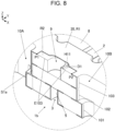
- FIG. 8 is an enlarged perspective view illustrating the area around the first cutout portion.
- the third top surface of the third substrate 103 includes a conductor region R1 where the metal layer 35 is positioned and a non-conductor region R2 where the metal layer 35 is not positioned.
- the non-conductor region R2 extends from a position P1 between the first recess 10A and the first cutout portion 9 to a position P2 between the first cutout portion 9 and the second recess 10B up to an outer edge E103 ( FIG. 8 ) of the third top surface of the third substrate 103.
- the outer edge E103 of the third top surface means the edge of the third top surface of the third substrate 103 on the side where the first outer surface S1a is located.
- the generation of burrs in the metal layer 35 can be reduced at the outer edge E103 of the third top surface from the position P1 to the position P2. Therefore, the occurrence of a situation in which conductors such as burrs are located on the first outer surface S1a in the vicinity of where the signal line 2 is positioned is reduced, and stable frequency characteristics are obtained. Furthermore, adjustment of the characteristic impedance of the signal transmission part 1b is easily realized by adjusting the area of the non-conductor region R2.
- the non-conductor region R2 includes a wider portion H11 ( FIG. 8 ) whose width D1 in the Y direction (direction perpendicular to the first outer surface S1a) increases with increasing proximity to the first cutout portion 9.
- the conductor region R1 extends across the entirety of an edge E10A ( FIG. 4 ) of the first recess 10A located on the third top surface of the third substrate 103, as well as the entirety of an edge E10B ( FIG. 4 ) of the second recess 10B located on the third top surface of the third substrate 103. This configuration stabilizes the ground potential of the metal layer 35.
- FIG. 9 is a diagram illustrating part of a semiconductor element mounting substrate of Variation 1. Part C1 illustrated in FIG. 9 corresponds to part C1 of FIG. 2A .
- the spacing W1 between the first recess 10A and the second recess 10B in the first substrate 101, the spacing W2 between the first recess 10A and the second recess 10B in the second substrate 102, and the spacing W3 between the first recess 10A and the second recess 10B in the third substrate 103 may be set to satisfy a condition (5).
- condition (6) may be satisfied.
- W 1 W 2
- condition (5) When condition (5) is satisfied, the spacing between the first side surface ground conductor 31A and the second side surface ground conductor 31B is smaller above the groove 3. Therefore, the cutoff frequency of a radio-frequency signal transmitted through the side surface conductor 5 inside the groove 3, the electrode 6, the through conductor 4, and the signal line 2 is increased, and the bandwidth of the frequency characteristics of the signal transmission part 1b is broadened. Furthermore, since the spacing between the groove 3 and the first recess 10A and the spacing between the groove 3 and the second recess 10B can be increased while achieving a wider bandwidth, the reliability of the semiconductor element mounting substrate 1 in terms of mounting can be improved.
- the first recess 10A and second recess 10B located in the first substrate 101 and the first recess 10A and second recess 10B located in the second substrate 102 can overlap in plan view in a large number of regions.
- the first side surface ground conductor 31A and the second side surface ground conductor 31B located on the first substrate 101 and the first side surface ground conductor 31A and the second side surface ground conductor 31B located on the second substrate 102 are continuous with each other. Therefore, the shapes of the first side surface ground conductor 31A and the second side surface ground conductor 31B can be stabilized and the ground potential of the signal transmission part 1b can be stabilized. Thus, the frequency characteristics of the signal transmission part 1b can be stabilized.
- FIGs. 10A to 10C illustrate a semiconductor element mounting substrate according to Variation 2.
- FIG. 10A is a perspective view of a semiconductor element mounting substrate 1A according to Variation 2 viewed from above
- FIG. 10B is a perspective view of the semiconductor element mounting substrate 1A viewed from below
- FIG. 10C is a sectional view taken along line A-A in FIG. 10A .
- the first substrate 101 may have an integrated configuration including the mounting region a and the peripheral region b.
- the semiconductor element mounting substrate 1A having this configuration does not include the gap 30 of the first substrate 101 illustrated in FIG. 3 , the first inner surface S1b of the first substrate 101, or the second cutout portion 41 illustrated in FIG. 5 .
- the rest of the configuration is substantially the same as that of the semiconductor element mounting substrate 1 of the above-described embodiment.
- the first substrate 101, the second substrate 102, and the third substrate 103 have the first outer surface S1a and adjacent outer surfaces S2a and S3a, a corner T1 positioned between the first outer surface S1a and the outer surface S2a, and a corner T2 positioned between the first outer surface S1a and the outer surface S3a.
- a second recess 10C may intersect the outer surface S2a, as illustrated in the signal transmission part 1d in FIG. 2A or FIG. 10A .
- a first recess 10D may intersect the outer surface S3a, as illustrated in the signal transmission part 1a in FIG. 2A or FIG. 10A .
- the outer surfaces S2a and S3a corresponding to examples of a second outer surface according to the present disclosure.
- the shapes of the first substrate 101, the second substrate 102, and the third substrate 103 in the vicinity of the corners T1 and T2 are simplified, and the risk of damage such as cracks occurring in the corners T1 and T2 can be reduced.
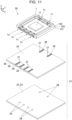
- FIG. 11 is an exploded perspective view of the semiconductor device in FIG. 1 .
- the semiconductor element 11 is placed on the mounting region a of the first substrate 101, the semiconductor element 11 is adhered and fixed to the first substrate 101 via an adhesive or the like, and the semiconductor element 11 and the signal line 2 are electrically connected to each other via bonding wires or the like.
- the semiconductor device 20 is completed as a product by mounting the semiconductor element 11 on the semiconductor element mounting substrate 1.
- a cover may be provided on the top surface of the semiconductor element mounting substrate 1.
- the semiconductor device 20 may further include a mounting substrate 21 bonded to the first bottom surface of the first substrate 101.
- the mounting substrate 21 includes multiple insulating layers, for example.
- Signal conductors 26 and second connection terminals 27 composed of a metal material such as copper foil are provided on the top surface of the uppermost insulating layer.
- the signal conductors 26 and the second connection terminals 27 are electrically connected to the side surface conductors 5 and the signal electrodes 33 on the first bottom surface via a conductive bonding material such as solder, and radio-frequency electrical signals are transmitted therethrough.
- the mounting substrate 21 is provided with the ground layer 25 as the uppermost layer.
- the ground layer 25 is composed of a metal material, such as copper foil, arranged at predetermined intervals on the top surface of the uppermost layer so as to sandwich the signal conductors 26 and surround the second connection terminals 27, and is maintained at the ground potential.
- the ground layer 25 is bonded to the metal layers 34 provided on the bottom surface of the semiconductor element mounting substrate 1, the first side surface ground conductors 31A, the second side surface ground conductors 31B, and the bottom surface of the mounting region a composed of a metal material via a bonding material such as solder.
- the mounting substrate 21 is provided with the above-described second connection terminals 27, signal conductors 26, and ground layer 25 on the top surface, and this allows so-called coplanar lines, which are one type of planar transmission lines, to be formed.
- the mounting substrate 21 may include a ground conductor 22 formed on an inner layer thereof.
- the ground conductor 22 includes a formed region 23 where the ground conductor 22 is formed and non-formed regions 24 where the ground conductor 22 is not formed.
- the non-formed regions 24 of the ground conductor layer are not provided, in plan view, at least at positions overlapping the signal electrodes 33 ( FIG. 6 ) on the first bottom surface and the second connection terminals 27. This configuration can reduce the difficulty of making adjustments to the desired characteristic impedance range when mounting the semiconductor device 20 on the mounting substrate 21. This is because if the non-formed regions 24 overlap the signal electrodes 33 ( FIG.
- the capacitances generated with the ground potential parts in the signal transmission portions between the signal conductors 26 and the side surface conductors 5 are increased by the conductive bonding material, such as solder, electrically connecting the signal electrodes 33 on the first bottom surface to the second connection terminals 27, and the meniscus formed on the side surfaces of the side surface conductors 5 by this bonding material, and the characteristic impedance is reduced.
- the conductive bonding material such as solder
- Each non-formed region 24 may be positioned, in plan view, inward from (on the side surface conductor 5 side) the first side surface ground conductor 31A and the second side surface ground conductor 31B between which the side surface conductor 5 is interposed in a direction perpendicular to the signal transmission direction of the signal line 2 (i.e., direction from the signal line 2 to the semiconductor element 11).
- the present disclosure is not limited to the embodiments described above, and can be modified in various ways without departing from the gist of the present disclosure.
- the spacings W1, W2, and W3, as well as the widths W21, W22, W23, W25a, and W25b, described above, do not need to be constant from the top to the bottom of the corresponding region. If the value differs depending on the height of the measurement, a representative value may be obtained from values measured at multiple heights obtained by equally dividing the corresponding region from top to bottom, and the representative value may be used as the value for the spacings W1, W2, and W3, and the widths W21, W22, W23, W25a, and W25b.
- the central 80% of measured values may be extracted from measured values at the multiple heights, and the average of the extracted measured values may be adopted as the representative value.
- the present disclosure can be used in a semiconductor element mounting substrate and a semiconductor device.
Landscapes
- Engineering & Computer Science (AREA)
- Microelectronics & Electronic Packaging (AREA)
- Structure Of Printed Boards (AREA)
- Physics & Mathematics (AREA)
- Geometry (AREA)
Abstract
Description
- The present disclosure relates to a semiconductor element mounting substrate and a semiconductor device.
- International Publication No.
2018/021209 discloses a semiconductor element mounting substrate and a semiconductor device. The semiconductor element mounting substrate includes a first substrate, a frame-shaped second substrate, and a frame-shaped third substrate. The first substrate has a top surface including a mounting region for mounting a semiconductor element and a peripheral region. The second substrate is positioned on the peripheral region of the first substrate. The third substrate is positioned on the second substrate. - In the present disclosure, a semiconductor element mounting substrate includes a first substrate, a frame-shaped second substrate, and a frame-shaped third substrate.
- The first substrate has a first top surface including a mounting region allowing mounting of a semiconductor element and a peripheral region surrounding the mounting region.
- The second substrate is positioned on the peripheral region of the first substrate and surrounds the mounting region.
- The third substrate is positioned on the second substrate and surrounds the mounting region.
- The first substrate, the second substrate, and the third substrate have a common outward facing first outer surface.
- The semiconductor element mounting substrate further includes a groove, a signal line, a through conductor, a side surface conductor, a first cutout portion, a first recess, a second recess, a first side surface ground conductor, and a second side surface ground conductor.
- The groove is positioned extending from the first top surface to a first bottom surface of the first substrate on the first outer surface.
- The signal line is positioned on a second top surface of the second substrate. The through conductor is positioned inside the second substrate and is connected to the signal line.
- The side surface conductor is positioned on an inner surface of the groove and electrically connected to the through conductor.
- The first cutout portion is positioned on the first outer surface of the third substrate and overlaps the groove in planar perspective view.
- The first recess and the second recess are positioned extending from a third top surface of the third substrate to the first bottom surface of the first substrate in the first outer surface and positioned side by side with the groove interposed therebetween.
- The first side surface ground conductor and the second side surface ground conductor are respectively positioned on an inner surface of the first recess and an inner surface of the second recess.
- A width reduction portion is provided between the first recess and the second recess, a spacing between the first recess and the second recess being smaller at a top of the width reduction portion than at a bottom of the width reduction portion.
- In the present disclosure, a semiconductor device includes the above semiconductor element mounting substrate and a semiconductor element.
- The semiconductor element is mounted on the mounting region and is electrically connected to the signal line.
-
-
FIG. 1 is a perspective view illustrating a semiconductor device according to an embodiment of the present disclosure. -
FIG. 2A is a perspective view in which a semiconductor element mounting substrate according toEmbodiment 1 of the present disclosure is viewed from above. -
FIG. 2B is a perspective view in which the semiconductor element mounting substrate according toEmbodiment 1 of the present disclosure is viewed from below. -
FIG. 2C is a perspective view in which the semiconductor element mounting substrate according toEmbodiment 1 of the present disclosure is viewed from below with a main portion of a first substrate removed. -
FIG. 3 is a sectional view taken along line A-A inFIG. 2A . -
FIG. 4 is an enlarged view of part C1 ofFIG. 2A . -
FIG. 5 is an enlarged view of part C2 ofFIG. 2C . -
FIG. 6 is a diagram mainly illustrating signal conductors in part C2 ofFIG. 2C . -
FIG. 7 is a diagram mainly illustrating internal ground conductors in part C2 ofFIG. 2C . -
FIG. 8 is an enlarged perspective view illustrating the area around a first cutout portion. -
FIG. 9 is a diagram illustrating part of a semiconductor element mounting substrate ofVariation 1. -
FIG. 10A is a perspective view in which a semiconductor element mounting substrate ofVariation 2 is viewed from above. -
FIG. 10B is a perspective view in which the semiconductor element mounting substrate ofVariation 2 is viewed from below. -
FIG. 10C is a sectional view taken along line A-A inFIG. 10A . -
FIG. 11 is an exploded perspective view of a semiconductor device inFIG. 1 . - Hereafter, embodiments of the present disclosure will be described in detail while referring to the drawings.
-
FIG. 1 is a perspective view illustrating a semiconductor device according to an embodiment of the present disclosure.FIGs. 2A to 2C illustrate a semiconductor element mounting substrate according toEmbodiment 1 of the present disclosure.FIG. 2A is a perspective view in which a semiconductorelement mounting substrate 1 according toEmbodiment 1 is viewed from above.FIG. 2B is a perspective view in which the semiconductorelement mounting substrate 1 is viewed from below.FIG. 2C is a perspective view in which the semiconductorelement mounting substrate 1 is viewed from below with a main portion of a first substrate removed.FIG. 3 is a sectional view taken along line A-A inFIG. 2A . Hereafter, the directions of each part are represented with a direction from afirst substrate 101 toward a third substrate 103 (Z direction) being an upward direction and direction parallel to a substrate surface of the first substrate 101 (X-Y plane direction) being a horizontal direction. These directions do not need to match the directions at the time of use of the semiconductorelement mounting substrate 1 or asemiconductor device 20. In order to avoid confusion, in this specification, the top surface of thefirst substrate 101 is referred to as a first top surface S101 and the bottom surface of thefirst substrate 101 is referred to as a first bottom surface. Similarly, the top surface of asecond substrate 102 is referred to as a second top surface, the bottom surface of thesecond substrate 102 is referred to as a second bottom surface, the top surface of thethird substrate 103 is referred to as a third top surface and the bottom surface of thethird substrate 103 is referred to as a third bottom surface. - The
semiconductor device 20 and the semiconductorelement mounting substrate 1 include thefirst substrate 101, thesecond substrate 102, and thethird substrate 103. Thefirst substrate 101 may have a single layer structure or a multilayer structure in which multiple insulating layers are stacked on top of one another. In the case of a multilayer structure, thefirst substrate 101 may include metal films positioned between the multiple insulating layers. This also applies to thesecond substrate 102 and thethird substrate 103. A multilayer structure facilitates the design of signal wiring having a multilayer structure. - The
first substrate 101 has the first top surface S101. The first top surface S101 includes a mounting region a that allows mounting of asemiconductor element 11 and a peripheral region b that surrounds the mounting region a. Thefirst substrate 101 is composed of a ceramic such as an alumina (Al2O3) sintered material (alumina ceramic), for example. - The
second substrate 102 is positioned on the peripheral region b of thefirst substrate 101. When viewed in plan view (when viewed in the Z direction), an outer edge of thesecond substrate 102 overlaps an outer edge of thefirst substrate 101 for the most part. Thesecond substrate 102 has a frame-like shape surrounding the mounting region a. Similarly to thefirst substrate 101, thesecond substrate 102 is composed of a ceramic such as an alumina (Al2O3) sintered material (alumina ceramic), for example. - The
third substrate 103 has a frame-like shape surrounding the mounting region a. Thethird substrate 103 is positioned on thesecond substrate 102. When viewed in plan view, an outer edge of thethird substrate 103 overlaps the outer edge of thesecond substrate 102 for the most part. In plan view, an inner edge of thethird substrate 103 may be positioned outward from an inner edge of thesecond substrate 102. Thethird substrate 103 is composed of the same material as thefirst substrate 101 and thesecond substrate 102, for example. - As illustrated in
FIGs. 2A, 2B , and3 , thefirst substrate 101 includes amain portion 101a containing the mounting region a and aframe portion 101b containing the peripheral region b. Agap 30 may be positioned between themain portion 101a and theframe portion 101b. Thefirst substrate 101 may be divided into themain portion 101a and theframe portion 101b, or part of themain portion 101a and part of theframe portion 101b may be connected to each other. - Temperature changes or temperature gradients occur inside the semiconductor
element mounting substrate 1 during the process of manufacturing the semiconductorelement mounting substrate 1 or thesemiconductor device 20, or due to heat generated by thesemiconductor element 11 when thesemiconductor device 20 is operated. Stress may then occur due to thermal expansion and thermal contraction of the semiconductorelement mounting substrate 1 or thesemiconductor element 11. Even in such a case, the stress generated in the semiconductorelement mounting substrate 1 can be relieved by the presence of thegap 30, and therefore the occurrence of damage and cracks in the semiconductorelement mounting substrate 1 can be reduced. In addition, since deformation and warping of the mounting region a caused by deformation and warping of the semiconductorelement mounting substrate 1 can be reduced, thesemiconductor element 11 can be stably mounted in the mounting region a. In addition, damage to thesemiconductor element 11 caused by deformation or warping of the mounting region a can be reduced. - When the
first substrate 101 is divided into themain portion 101a and theframe portion 101b, themain portion 101a may be composed of a metal material. Iron, copper, nickel, chromium, cobalt, tungsten, molybdenum, or an alloy composed of these metals can be used as the metal material. The mounting region a may be electrically connected to a firstground conductor layer 7, which is described below, with a conductive bonding material such as solder or a brazing material. With this configuration, as well as heat dissipation of the semiconductorelement mounting substrate 1 being improved, since the firstground conductor layer 7, second ground conductor layers 8, first sidesurface ground conductors 31A, and second sidesurface ground conductors 31B, which are described below, are connected to aground layer 25 provided on an external mounting substrate described below via the mounting region a, the respective ground potentials are stabilized. In addition, the bonding area between the mounting region a, where the ground potential of semiconductorelement mounting substrate 1 is applied, and the ground conductor provided on the external mounting substrate can be made larger, and consequently the ground potential of semiconductorelement mounting substrate 1, including the mounting region a, is further stabilized. Therefore, the frequency characteristics in signal transmission portions of the semiconductorelement mounting substrate 1 can be further improved. - The
first substrate 101, thesecond substrate 102, and thethird substrate 103 have a common first outer surface S1a, which faces outward, and a first inner surface S1b positioned on the opposite side from the first outer surface S1a. The first inner surface S1b faces the inside of the semiconductorelement mounting substrate 1. As illustrated inFIG. 3 , in thefirst substrate 101, the first inner surface S1b faces thegap 30. The first inner surface S1b in thesecond substrate 102 may extend inward to a greater extent than the first inner surface S1b of thefirst substrate 101 and the first inner surface S1b of thethird substrate 103. - The semiconductor
element mounting substrate 1 includes a plurality ofsignal transmission parts 1a to 1f, for example. Onesignal transmission part 1b, which is positioned between the first outer surface S1a and the first inner surface S1b, is described below. Thesignal transmission part 1b has the same or substantially the same configuration as the othersignal transmission parts -
FIG. 4 is an enlarged view of part C1 ofFIG. 2A .FIG. 5 is an enlarged view of part C2 ofFIG. 2C .FIG. 6 is a diagram mainly illustrating signal conductors in part C2 ofFIG. 2C . Although thesignal transmission part 1f is illustrated in part C2 ofFIG. 2C ,FIGs. 5 to 7 illustrate thesignal transmission part 1b as viewed from the first inner surface S1b. InFIGs. 4 and5 , conductor portions are indicated by shading. - The semiconductor
element mounting substrate 1 includes asignal line 2, agroove 3, a throughconductor 4, aside surface conductor 5, anelectrode 6, aconnection terminal 28, and asignal electrode 33 as constituent parts of thesignal transmission part 1b. - The
signal line 2 is positioned on the second top surface of thesecond substrate 102 and extends from one end, on the inner edge side, of thesecond substrate 102 to above the peripheral region b. Thesignal line 2 is composed of, for example, iron, copper, nickel, gold, chromium, cobalt, molybdenum, manganese, tungsten, or an alloy of these materials. Thesignal line 2 is connected to thesemiconductor element 11. - The
groove 3 is positioned in the first outer surface S1a of thefirst substrate 101 and extends from the first top surface S101 to the first bottom surface of thefirst substrate 101. - The
side surface conductor 5 extends across the inner surface of thegroove 3 and is electrically connected to thesignal line 2, and theelectrode 6 and the throughconductor 4, which are described later, and conducts a radio-frequency signal therethrough. Theside surface conductor 5 is composed of, for example, iron, copper, nickel, gold, chromium, cobalt, molybdenum, manganese, tungsten, or an alloy of these materials. - The
groove 3 is positioned inward from the outer edge of thesecond substrate 102. Therefore, thesecond substrate 102 protrudes outward at the place where thegroove 3 is located. With this configuration, the risk of theside surface conductor 5 formed in thegroove 3 being damaged or short-circuited due to external influences is reduced, and the electrical conductivity of theside surface conductor 5 can be maintained in a good state. In planar perspective view, the outer edge of thesecond substrate 102 may be positioned outward from the outer edge of thefirst substrate 101. With this configuration, since thesecond substrate 102, which is located above thegroove 3, protrudes outward, the risk of theside surface conductor 5 formed in thegroove 3 being damaged or short-circuited due to external influences is further reduced, and the electrical conductivity of theside surface conductor 5 can be maintained in a good state. - The
side surface conductor 5 inside thegroove 3 is electrically connected to an external mounting substrate via a conductive bonding material such as solder. When this connection is being formed, a meniscus is formed at the lower edge of the inner surface of thegroove 3 by the bonding material. As a result of this action, theside surface conductor 5 is electrically connected to the external mounting substrate in a stable manner. Therefore, the semiconductorelement mounting substrate 1 can reduce fluctuations in the characteristic impedance in the signal transmission portions and improve the frequency characteristics. - The
groove 3 includes a curved portion in planar perspective view. More specifically, thegroove 3 may have a semi-circular shape (semi-circular, semi-elliptical, elongated semi-circular, etc.) for example, in planar perspective view. Temperature changes or temperature gradients occur inside the semiconductorelement mounting substrate 1 during the process of manufacturing the semiconductorelement mounting substrate 1 or thesemiconductor device 20, or due to heat generated by thesemiconductor element 11 when thesemiconductor device 20 is operated. Stress may then occur due to thermal expansion and thermal contraction of the semiconductorelement mounting substrate 1. In this case, the concentration of stress in the vicinity of thegroove 3 can be reduced as a result of thegroove 3 including the curved portion, and the occurrence of damage or cracks in thefirst substrate 101, theside surface conductor 5, theelectrode 6, thesignal electrode 33 on the first bottom surface, the first sidesurface ground conductor 31A and the second sidesurface ground conductor 31B can be reduced. - The through conductor 4 (
FIG. 6 ) is electrically connected to thesignal line 2 and is positioned so as to extend from the second top surface to the second bottom surface of thesecond substrate 102. The throughconductor 4 is further electrically connected to theside surface conductor 5 via theelectrode 6 provided around the upper end of thegroove 3 on the first top surface of thefirst substrate 101. The throughconductor 4 is at a position that overlaps the other end of thesignal line 2 and is electrically connected to the other end of thesignal line 2. In this case, a radio-frequency electrical signal can be more reliably transmitted from the throughconductor 4 to thesignal line 2, and transmission loss and reflection loss of the transmitted radio-frequency electrical signal can be reduced. - The electrode 6 (
FIG. 6 ) is positioned on the first top surface of thefirst substrate 101 or the second bottom surface of thesecond substrate 102, between thefirst substrate 101 and thesecond substrate 102, and is electrically connected to theside surface conductor 5. Theelectrode 6 is a signal conductor layer positioned inside semiconductorelement mounting substrate 1. More specifically, theelectrode 6 may be provided around the upper end of the groove 3 (the end on thesecond substrate 102 side) in a direction (X-Y direction) perpendicular to the direction in which theside surface conductor 5 extends on the first top surface of thefirst substrate 101 or the second bottom surface of thesecond substrate 102, and electrically connected to theside surface conductor 5. Furthermore, in planar perspective view, the outer edge of theelectrode 6 may be positioned further toward the inside of the semiconductorelement mounting substrate 1 than the outer edge of theside surface conductor 5. In other words, theelectrode 6 may configured so as to not be positioned on the exposed part of the second bottom surface of thesecond substrate 102 above thegroove 3, i.e., so as to not be exposed on the second bottom surface of thesecond substrate 102. With this configuration, when thesemiconductor device 20 is electrically connected to the mounting substrate via a conductive bonding material such as solder, wet spreading of the bonding material onto theelectrode 6 via theside surface conductor 5 can be reduced. As a result, stress caused by a difference in thermal expansion coefficient between thesecond substrate 102 and the bonding material can be reduced. The possibility the characteristic impedance fluctuating in an unstable manner due to the wet spreading of the bonding material can also be reduced. As a result, the frequency characteristics in theside surface conductor 5 and theelectrode 6, which are signal transmission portions, can be maintained even better. - The
electrode 6 has a semi-circular (semi-circular, semi-elliptical, elongated semi-circular, etc.) outline (outline on side near mounting region a) in planar perspective view. This configuration allows theelectrode 6 to be easily formed in the process of manufacturing the semiconductorelement mounting substrate 1, and also reduces the possibility of stress being locally generated in the outline part of theelectrode 6. Furthermore, the semiconductorelement mounting substrate 1 can reduce unbalanced spreading of the electric field distribution in the vicinity of the outline of theelectrode 6. Therefore, the semiconductorelement mounting substrate 1 can reduce the risk of theelectrode 6 peeling off or cracks appearing in thefirst substrate 101 or thesecond substrate 102 due to stress generated in the outline part of theelectrode 6, and can further improve the frequency characteristics of the signal transmission portions. - The connection terminal 28 (
FIG. 6 ) protrudes from theelectrode 6 in the direction away from thegroove 3 and is positioned on the first top surface of thefirst substrate 101 or the second bottom surface of thesecond substrate 102. Theconnection terminal 28 is an inner layer connection terminal, and the throughconductor 4 is connected to a surface of the connection terminal on thesecond substrate 102 side. Via this connection, theelectrode 6 is electrically connected to thesignal line 2 via theconnection terminal 28 and the throughconductor 4. An increase in capacitances generated between theelectrode 6 and theconnection conductor 28 and the first ground conductor layer 7 (described below) and a reduction in the characteristic impedance of the signal transmission portions due to theelectrode 6 and theconnection conductor 28 can be suppressed by theconnection terminal 28. Therefore, the characteristic impedance of the signal transmission portions is easy to set to a desired value, and the semiconductorelement mounting substrate 1 can be reduced in size. In addition, the frequency characteristics in the signal transmission portions can be further improved. - The
connection terminal 28 may be positioned in a straight line from the center of the outer edge of the electrode 6 (the outer peripheral edge of the second substrate 102) in planar perspective view in the opposite direction from thegroove 3. With this configuration, the semiconductorelement mounting substrate 1 enables the length of the signal transmission portion consisting of theelectrode 6 and theconnection terminal 28 to be shortened, and enables further improvement of the frequency characteristics in the signal transmission portion. - The signal electrode 33 (
FIG. 6 ) is a film conductor that extends around thegroove 3 so as to surround thegroove 3 on the first bottom surface of thefirst substrate 101. Thesignal electrode 33 is connected to theside surface conductor 5 inside thegroove 3. Thesignal electrode 33 has a semi-circular (semi-circular, semi-elliptical, elongated semi-circular, etc.) outline (outline on side near mounting region a) when viewed in plan view. This configuration allows thesignal electrode 33 to be easily formed in the process of manufacturing the semiconductorelement mounting substrate 1, and also reduces the possibility of stress being locally generated in the outer edge part of thesignal electrode 33. Furthermore, when mounting thesemiconductor device 20 on an external mounting substrate via thesignal electrode 33 using a conductive bonding material such as solder, the occurrence of a situation in which stress generated around thesignal electrode 33 and the bonding material becomes concentrated in a single place can be reduced. Therefore, the semiconductorelement mounting substrate 1 can reduce the risk of thesignal electrode 33 peeling off or cracks occurring in thefirst substrate 101 due to stress generated in the above-mentioned outline part of theelectrode 6. Furthermore, with the above configuration of thesignal electrode 33, the semiconductorelement mounting substrate 1 is able to reduce the unbalanced spreading of the electric field distribution in the vicinity of the outline of thesignal electrode 33. In addition, thesignal electrode 33 can stabilize the electrical connection between thesemiconductor element 11 and the external mounting substrate. Therefore, the frequency characteristics of the signal transmission portion including thesignal electrode 33 can be improved. -
FIG. 7 is a diagram mainly illustrating internal ground conductors in part C2 ofFIG. 2C . InFIG. 7 , the firstground conductor layer 7 is represented with the center portion thereof cut away. - The semiconductor
element mounting substrate 1 further includes the firstground conductor layer 7, the second ground conductor layers 8, metal layers 34 and 35, afirst recess 10A, asecond recess 10B, the first sidesurface ground conductor 31A, and the second sidesurface ground conductor 31B as constituent parts of thesignal transmission part 1b. - The first
ground conductor layer 7, the second ground conductor layers 8, and the metal layers 34 and 35 may be configured to be integrated with each other in each of the plurality ofsignal transmission parts 1a to 1f. - The first
ground conductor layer 7 is positioned on the first top surface of thefirst substrate 101 or the second bottom surface of thesecond substrate 102, between thefirst substrate 101 and thesecond substrate 102, so as to be spaced apart from theelectrode 6. The firstground conductor layer 7 is a ground conductor layer positioned inside the semiconductorelement mounting substrate 1. The firstground conductor layer 7 may be positioned so as to surround theelectrode 6 inside the semiconductorelement mounting substrate 1, and this configuration can reduce the characteristic impedance in theside surface conductor 5 and theelectrode 6. Furthermore, the possibility of the electric field generated in the signal transmission portions from theside surface conductor 5 to the throughconductor 4 spreading into unintended areas via theelectrode 6 can be reduced, and the electric field can couple theelectrode 6 and the firstground conductor layer 7 to each other. Therefore, spreading of the electric field distribution of the signal transmission portions can be reduced. In addition, a radio-frequency electrical signal can be transmitted with electric field coupling between theelectrode 6 and the firstground conductor layer 7. In addition, the characteristic impedance in the above signal transmission portions can be stabilized. - The second ground conductor layers 8 are positioned on the second top surface of the
second substrate 102 so that thesignal line 2 is interposed therebetween. This configuration allows a so-called coplanar line configuration to be formed in which the signal transmission portion is interposed between ground potential parts on the second top surface of thesecond substrate 102. Therefore, the frequency characteristics in the signal transmission portion including thesignal line 2 can be further improved. The firstground conductor layer 7 may be positioned at a location overlapping thesignal line 2 and the second ground conductor layers 8 when viewed in perspective view in the Z direction. With this configuration, the signal transmission portion including thesignal line 2 is configured as a so-called coplanar line with a ground, and the frequency characteristics in the signal transmission portion can be further improved. The second ground conductor layers 8 may be partially positioned between thesecond substrate 102 and thethird substrate 103. - The metal layers 34 are connected to the first side
surface ground conductor 31A and the second sidesurface ground conductor 31B and extend on the first bottom surface of thefirst substrate 101. The metal layers 34 are positioned on the first bottom surface of thefirst substrate 101 so that thesignal line 2 is interposed therebetween in planar perspective view. The presence of the metal layers 34 on the first bottom surface makes forming an electrical connection with the mounting substrate easier. In addition, dissipation of heat of semiconductorelement mounting substrate 1 is improved through the metal layers 34. - The
metal layer 35 is connected to the first sidesurface ground conductor 31A and the second sidesurface ground conductor 31B and extends on the third top surface of thethird substrate 103. The presence of themetal layer 35 allows the electric field generated when a radio-frequency electrical signal is transmitted through thesignal line 2 to couple to themetal layer 35 on the third top surface, and thus the spreading of an unwanted and unstable electric field distribution around thesignal line 2 can be reduced. Therefore, the frequency characteristics in the signal transmission portions of the semiconductorelement mounting substrate 1 can be further improved. - The
first recess 10A and thesecond recess 10B are positioned to extend from the third top surface of thethird substrate 103 to the first bottom surface of thefirst substrate 101 on the first outer surface S1a. Viewed in the Y direction (direction perpendicular to the first outer surface S1a), thefirst recess 10A and thesecond recess 10B are positioned side by side with thegroove 3 interposed therebetween. Thefirst recess 10A and thesecond recess 10B are positioned so as to be spaced apart from thegroove 3 on both sides of thegroove 3. - The first side
surface ground conductor 31A is positioned on the inner surface of thefirst recess 10A. The second sidesurface ground conductor 31B is positioned on the inner surface of thesecond recess 10B. With this configuration, the first sidesurface ground conductor 31A and the second sidesurface ground conductor 31B are positioned so that theside surface conductor 5 through which a radio-frequency signal is conducted is interposed therebetween, and therefore the signal transmission portion is interposed between ground potential parts on the first outer surface S1a as well, and unwanted and unstable spreading of the electric field distribution and fluctuations in the characteristic impedance in the signal transmission portion of semiconductorelement mounting substrate 1 can be reduced. Therefore, the frequency characteristics of the semiconductorelement mounting substrate 1 can be further improved. - The first side
surface ground conductor 31A may be continuous across thefirst substrate 101, thesecond substrate 102, and thethird substrate 103. Furthermore, the first sidesurface ground conductor 31A may be positioned so as to extend across the entire inner surface of thefirst recess 10A. The second sidesurface ground conductor 31B may be continuous across thefirst substrate 101, thesecond substrate 102, and thethird substrate 103. Furthermore, the second side surface ground conductor 31BA may be positioned so as to extend across the entire inner surface of thesecond recess 10B. This configuration allows the areas of the first sidesurface ground conductor 31A and the second sidesurface ground conductor 31B to be increased. Therefore, the ground potential of the semiconductorelement mounting substrate 1 can be stabilized, and unnecessary and unstable spreading of the electric field distribution and fluctuations in the characteristic impedance around theside surface conductor 5 can be more stably reduced. - The portion of the first side
surface ground conductor 31A located on thefirst substrate 101, the portion of the first sidesurface ground conductor 31A located on thesecond substrate 102, and the portion of the first sidesurface ground conductor 31A located on thethird substrate 103 may overlap each other, at least to some extent, when viewed in planar perspective view. With this configuration, the semiconductorelement mounting substrate 1 can further reduce unnecessary and unstable spreading of the electric field distribution and fluctuations in the characteristic impedance that occur in the signal transmission portions of the semiconductorelement mounting substrate 1. This also applies to the second sidesurface ground conductor 31B. - The semiconductor
element mounting substrate 1 further includes afirst cutout portion 9, asecond cutout portion 41, andinner surface grooves 32 as constituent parts of thesignal transmission part 1b. - The first cutout portion 9 (
FIG. 4 ) is positioned on the first outer surface S1a of thethird substrate 103 and overlaps thegroove 3 in planar perspective view. Thefirst cutout portion 9 has a concave shape and may be positioned so as to extend from the third top surface to the third bottom surface of thethird substrate 103. No ground conductor is positioned on the inner surface of thefirst cutout portion 9. When the semiconductorelement mounting substrate 1 is reduced in size, the distances between thesignal line 2 and the surrounding ground conductors become smaller, and this increases the capacitances between the signal transmission portions and the ground potential parts, and characteristic impedance may be reduced. However, thefirst cutout portion 9 is able to reduce the above capacitances and suppress the reduction in the characteristic impedance. - The
first cutout portion 9 may have a larger outer shape than thegroove 3 in plan view. With this configuration, the semiconductorelement mounting substrate 1 can reduce the concentration of stress in thesecond substrate 102 positioned between thegroove 3 and thefirst cutout portion 9. Therefore, the possibility of cracks or splits occurring in thesecond substrate 102 can be reduced. - A width W21 (
FIG. 4 ) of thefirst cutout portion 9 in the X-direction (direction along the outer edge of the third top surface of the third substrate 103) may be smaller than a width W25a (FIG. 4 ), in the X-direction, of thefirst recess 10A located in thethird substrate 103, or a width W25b (FIG. 4 ), in the X-direction, of thesecond recess 10B located in thethird substrate 103. The X direction may be defined as a horizontal direction (first direction) along the first outer surface S1a. If the distance between thefirst recess 10A and thefirst cutout portion 9 and between thesecond recess 10B and thefirst cutout portion 9 is too small, the outwardly protruding portions of thethird substrate 103 will be small and easily damaged. Therefore, the strength of thethird substrate 103 is easily retained by reducing the width W21 of thefirst cutout portion 9 and securing the outwardly protruding portions. - The second cutout portion 41 (
FIG. 5 ) is positioned on the first inner surface S1b of thefirst substrate 101. Thesecond cutout portion 41 may overlap thegroove 3 when viewed in perspective view in the Y direction (direction perpendicular to the first outer surface S1a). Thesecond cutout portion 41 has a concave shape and may be positioned so as to extend from the first top surface to the first bottom surface of thefirst substrate 101. No ground conductor is positioned on the inner surface of thesecond cutout portion 41. The thickness of the ceramic (dielectric) of thefirst substrate 101 located in the Y direction of thegroove 3 is reduced by thesecond cutout portion 41. Thus, the effective dielectric constant around theside surface conductor 5 in thegroove 3 is reduced. Therefore, the characteristic impedance of the signal transmission portion is easily set to a desired value by adjusting the thickness (thickness in the Y direction) of thesecond cutout portion 41, and the frequency characteristics of the signal transmission portion can be further improved, for example, by reducing the reflection characteristics in a low frequency band. - A width W22 (
FIG. 5 ) of thesecond cutout portion 41 in the X direction (direction along the outer edge of the third top surface of the third substrate 103) may be larger than a width W23 (FIG. 5 ) of thegroove 3 in the X direction. With this configuration, a reduction in impedance can be more easily suppressed by making the width W22 of thesecond cutout portion 41 larger than the width of the side surface conductor 5 (corresponding to the width W23) along which a radio-frequency signal is transmitted. - Furthermore, the width W22 (
FIG. 5 ) of thesecond cutout portion 41 in the X direction may be larger than the width W21 (FIG. 4 ) of thefirst cutout portion 9 in the X direction. - The
inner surface grooves 32 are positioned on the first inner surface S1b of thethird substrate 103 and thesignal line 2 is interposed therebetween in the X direction (direction along the outer edge of the third top surface of the third substrate 103) when viewed in plan view. Theinner surface grooves 32 are positioned so as to extend from the third top surface to the third bottom surface of thethird substrate 103. Inner surface ground conductors, which are at the ground potential, are positioned on the inner surfaces of theinner surface grooves 32. Theinner surface grooves 32, where the inner surface ground conductors are positioned, can reduce unnecessary and unstable spreading of the electric field distribution at the end of thesignal line 2 on the side where the mounting region a is located, and can reduce fluctuations in the characteristic impedance of thesignal transmission part 1b. - The
groove 3 is positioned between thefirst recess 10A and thesecond recess 10B on the first outer surface S1a. A width reduction portion H1 (FIG. 4 ) is provided between thefirst recess 10A and thesecond recess 10B. The spacing between thefirst recess 10A and thesecond recess 10B is smaller at the top of the width reduction portion H1 (positive direction of the Z axis) than at the bottom of the width reduction portion H1 (negative direction of the Z axis). - The width reduction portion H1 may be positioned within a height range that includes the upper end of the
groove 3, or in a height range extending higher than thegroove 3. In the width reduction portion H1, the spacing between thefirst recess 10A and thesecond recess 10B may become smaller in a stepwise or gradual manner. The width reduction portion H1 allows the spacing between thefirst recess 10A and thesecond recess 10B at the top of the width reduction portion H1 to be smaller than the spacing would be without the presence of the width reduction portion H1. Therefore, the spacing between the first sidesurface ground conductor 31A and the second sidesurface ground conductor 31B can be made smaller at the top of the width reduction portion H1. Making this spacing smaller increases the cutoff frequency of radio-frequency signals transmitted through theside surface conductor 5 inside thegroove 3, theelectrode 6, the throughconductor 4, and thesignal line 2, and broadens the bandwidth of the frequency characteristics of thesignal transmission part 1b. Furthermore, the presence of the width reduction portion H1 enables the spacing between thegroove 3 and thefirst recess 10A and the spacing between thegroove 3 and thesecond recess 10B on the first bottom surface of thefirst substrate 101 to be increased. When the semiconductorelement mounting substrate 1 is mounted on a mounting substrate, thesignal electrode 33 and the metal layers 34 of the semiconductorelement mounting substrate 1 are bonded to a signal electrode and ground electrodes of the mounting substrate via a conductive bonding material such as solder. Therefore, the risk of thesignal electrode 33 and the metal layers 34 being short circuited by the conductive bonding material spreading on the first bottom surface of thefirst substrate 101 during the bonding process can be reduced by increasing the spacing between thegroove 3 and thefirst recess 10A and the spacing between thegroove 3 and thesecond recess 10B. Therefore, the reliability of semiconductorelement mounting substrate 1 in terms of mounting can be improved. - A spacing W1 between the
first recess 10A and thesecond recess 10B in thefirst substrate 101, a spacing W2 between thefirst recess 10A and thesecond recess 10B in thesecond substrate 102, and a spacing W3 between thefirst recess 10A and thesecond recess 10B in thethird substrate 103 may be set to satisfy the following conditions (1) and (2).
- With this configuration, the spacing between the
first recess 10A and thesecond recess 10B is smaller at the top between thefirst substrate 101 and thesecond substrate 102, or between thesecond substrate 102 and thethird substrate 103. As a result of the spacing between the first sidesurface ground conductor 31A and the second sidesurface ground conductor 31B being smaller at the top, the cutoff frequency of radio-frequency signals transmitted through theside surface conductor 5 in thegroove 3, theelectrode 6, the throughconductor 4, and thesignal line 2 is increased and the bandwidth of the frequency characteristics ofsignal transmission part 1b is broadened. Furthermore, since the spacing between thegroove 3 and thefirst recess 10A and the spacing between thegroove 3 and thesecond recess 10B can be increased while achieving a wider bandwidth, the reliability of the semiconductorelement mounting substrate 1 in terms of mounting can be improved. - Furthermore, the spacings W1 to W3 may satisfy the following condition (3).

first recess 10A and thesecond recess 10B, i.e., the spacing between the first sidesurface ground conductor 31A and the second sidesurface ground conductor 31B, can be made smaller at the height where the throughconductor 4 is located, and the bandwidth of the frequency characteristics of thesignal transmission part 1b can be broadened. - Furthermore, the spacings W1 to W3 may satisfy the following condition (4).

- With this configuration, the
first recess 10A andsecond recess 10B located in thesecond substrate 102 and thefirst recess 10A andsecond recess 10B located in thethird substrate 103 can include many overlapping regions in plan view. In the overlapped regions, the first sidesurface ground conductor 31A and the second sidesurface ground conductor 31B located on thesecond substrate 102 and the first sidesurface ground conductor 31A and the second sidesurface ground conductor 31B located on thethird substrate 103 are continuous with each other. Therefore, the shapes of the first sidesurface ground conductor 31A and the second sidesurface ground conductor 31B can be stabilized and the ground potential of thesignal transmission part 1b can be stabilized. Thus, the frequency characteristics of thesignal transmission part 1b can be stabilized. - If the spacing W2 is made too small, the bandwidth of the frequency characteristics is broadened and the reflection characteristics in a low-frequency band are degraded due to the decrease in the characteristic impedance. However, the characteristic impedance around the
side surface conductor 5 is increased by thesecond cutout portion 41, and as a result, the degradation of the reflection characteristics can be reduced. - The thickness (maximum dimension in Y direction) of the
first recess 10A may be uniform from thefirst substrate 101 to thethird substrate 103. The thickness (maximum dimension in Y direction) of thesecond recess 10B may be uniform from thefirst substrate 101 to thethird substrate 103. -
FIG. 8 is an enlarged perspective view illustrating the area around the first cutout portion. - The third top surface of the
third substrate 103 includes a conductor region R1 where themetal layer 35 is positioned and a non-conductor region R2 where themetal layer 35 is not positioned. The non-conductor region R2 extends from a position P1 between thefirst recess 10A and thefirst cutout portion 9 to a position P2 between thefirst cutout portion 9 and thesecond recess 10B up to an outer edge E103 (FIG. 8 ) of the third top surface of thethird substrate 103. The outer edge E103 of the third top surface means the edge of the third top surface of thethird substrate 103 on the side where the first outer surface S1a is located. With this configuration, when forming the first outer surface S1a by performing dicing or the like, the generation of burrs in themetal layer 35 can be reduced at the outer edge E103 of the third top surface from the position P1 to the position P2. Therefore, the occurrence of a situation in which conductors such as burrs are located on the first outer surface S1a in the vicinity of where thesignal line 2 is positioned is reduced, and stable frequency characteristics are obtained. Furthermore, adjustment of the characteristic impedance of thesignal transmission part 1b is easily realized by adjusting the area of the non-conductor region R2. - The non-conductor region R2 includes a wider portion H11 (
FIG. 8 ) whose width D1 in the Y direction (direction perpendicular to the first outer surface S1a) increases with increasing proximity to thefirst cutout portion 9. With this configuration, the impedance of a radio-frequency signal conducted from thesignal line 2 to theside surface conductor 5 can be easily reduced. - The conductor region R1 extends across the entirety of an edge E10A (
FIG. 4 ) of thefirst recess 10A located on the third top surface of thethird substrate 103, as well as the entirety of an edge E10B (FIG. 4 ) of thesecond recess 10B located on the third top surface of thethird substrate 103. This configuration stabilizes the ground potential of themetal layer 35. -
FIG. 9 is a diagram illustrating part of a semiconductor element mounting substrate ofVariation 1. Part C1 illustrated inFIG. 9 corresponds to part C1 ofFIG. 2A . - As illustrated in
FIG. 9 , the spacing W1 between thefirst recess 10A and thesecond recess 10B in thefirst substrate 101, the spacing W2 between thefirst recess 10A and thesecond recess 10B in thesecond substrate 102, and the spacing W3 between thefirst recess 10A and thesecond recess 10B in thethird substrate 103 may be set to satisfy a condition (5).

- When condition (5) is satisfied, the spacing between the first side
surface ground conductor 31A and the second sidesurface ground conductor 31B is smaller above thegroove 3. Therefore, the cutoff frequency of a radio-frequency signal transmitted through theside surface conductor 5 inside thegroove 3, theelectrode 6, the throughconductor 4, and thesignal line 2 is increased, and the bandwidth of the frequency characteristics of thesignal transmission part 1b is broadened. Furthermore, since the spacing between thegroove 3 and thefirst recess 10A and the spacing between thegroove 3 and thesecond recess 10B can be increased while achieving a wider bandwidth, the reliability of the semiconductorelement mounting substrate 1 in terms of mounting can be improved. - By satisfying condition (6), the
first recess 10A andsecond recess 10B located in thefirst substrate 101 and thefirst recess 10A andsecond recess 10B located in thesecond substrate 102 can overlap in plan view in a large number of regions. In the regions that overlap in plan view, the first sidesurface ground conductor 31A and the second sidesurface ground conductor 31B located on thefirst substrate 101 and the first sidesurface ground conductor 31A and the second sidesurface ground conductor 31B located on thesecond substrate 102 are continuous with each other. Therefore, the shapes of the first sidesurface ground conductor 31A and the second sidesurface ground conductor 31B can be stabilized and the ground potential of thesignal transmission part 1b can be stabilized. Thus, the frequency characteristics of thesignal transmission part 1b can be stabilized. -
FIGs. 10A to 10C illustrate a semiconductor element mounting substrate according toVariation 2.FIG. 10A is a perspective view of a semiconductorelement mounting substrate 1A according toVariation 2 viewed from above,FIG. 10B is a perspective view of the semiconductorelement mounting substrate 1A viewed from below, andFIG. 10C is a sectional view taken along line A-A inFIG. 10A . As illustrated inFIGs. 10A to 10C , thefirst substrate 101 may have an integrated configuration including the mounting region a and the peripheral region b. The semiconductorelement mounting substrate 1A having this configuration does not include thegap 30 of thefirst substrate 101 illustrated inFIG. 3 , the first inner surface S1b of thefirst substrate 101, or thesecond cutout portion 41 illustrated inFIG. 5 . The rest of the configuration is substantially the same as that of the semiconductorelement mounting substrate 1 of the above-described embodiment. - In the semiconductor
element mounting substrate 1A ofVariation 2, the same or similar effects are achieved by the constituent parts common to the semiconductorelement mounting substrate 1 described inEmbodiment 1. - As illustrated in
FIG. 2A orFIG. 10A , thefirst substrate 101, thesecond substrate 102, and thethird substrate 103 have the first outer surface S1a and adjacent outer surfaces S2a and S3a, a corner T1 positioned between the first outer surface S1a and the outer surface S2a, and a corner T2 positioned between the first outer surface S1a and the outer surface S3a. A second recess 10C may intersect the outer surface S2a, as illustrated in thesignal transmission part 1d inFIG. 2A orFIG. 10A . Similarly, afirst recess 10D may intersect the outer surface S3a, as illustrated in thesignal transmission part 1a inFIG. 2A orFIG. 10A . The outer surfaces S2a and S3a corresponding to examples of a second outer surface according to the present disclosure. - With this configuration, the shapes of the
first substrate 101, thesecond substrate 102, and thethird substrate 103 in the vicinity of the corners T1 and T2 are simplified, and the risk of damage such as cracks occurring in the corners T1 and T2 can be reduced. -
FIG. 11 is an exploded perspective view of the semiconductor device inFIG. 1 . When assembling thesemiconductor device 20, thesemiconductor element 11 is placed on the mounting region a of thefirst substrate 101, thesemiconductor element 11 is adhered and fixed to thefirst substrate 101 via an adhesive or the like, and thesemiconductor element 11 and thesignal line 2 are electrically connected to each other via bonding wires or the like. In this way, thesemiconductor device 20 is completed as a product by mounting thesemiconductor element 11 on the semiconductorelement mounting substrate 1. Although not illustrated, a cover may be provided on the top surface of the semiconductorelement mounting substrate 1. - The
semiconductor device 20 may further include a mountingsubstrate 21 bonded to the first bottom surface of thefirst substrate 101. The mountingsubstrate 21 includes multiple insulating layers, for example.Signal conductors 26 andsecond connection terminals 27 composed of a metal material such as copper foil are provided on the top surface of the uppermost insulating layer. Thesignal conductors 26 and thesecond connection terminals 27 are electrically connected to theside surface conductors 5 and thesignal electrodes 33 on the first bottom surface via a conductive bonding material such as solder, and radio-frequency electrical signals are transmitted therethrough. Furthermore, the mountingsubstrate 21 is provided with theground layer 25 as the uppermost layer. Theground layer 25 is composed of a metal material, such as copper foil, arranged at predetermined intervals on the top surface of the uppermost layer so as to sandwich thesignal conductors 26 and surround thesecond connection terminals 27, and is maintained at the ground potential. - The
ground layer 25 is bonded to the metal layers 34 provided on the bottom surface of the semiconductorelement mounting substrate 1, the first sidesurface ground conductors 31A, the second sidesurface ground conductors 31B, and the bottom surface of the mounting region a composed of a metal material via a bonding material such as solder. The mountingsubstrate 21 is provided with the above-describedsecond connection terminals 27,signal conductors 26, andground layer 25 on the top surface, and this allows so-called coplanar lines, which are one type of planar transmission lines, to be formed. - The mounting
substrate 21 may include a ground conductor 22 formed on an inner layer thereof. The ground conductor 22 includes a formed region 23 where the ground conductor 22 is formed andnon-formed regions 24 where the ground conductor 22 is not formed. Thenon-formed regions 24 of the ground conductor layer are not provided, in plan view, at least at positions overlapping the signal electrodes 33 (FIG. 6 ) on the first bottom surface and thesecond connection terminals 27. This configuration can reduce the difficulty of making adjustments to the desired characteristic impedance range when mounting thesemiconductor device 20 on the mountingsubstrate 21. This is because if thenon-formed regions 24 overlap the signal electrodes 33 (FIG. 6 ) and thesecond connection terminals 27, the capacitances generated with the ground potential parts in the signal transmission portions between thesignal conductors 26 and theside surface conductors 5 are increased by the conductive bonding material, such as solder, electrically connecting thesignal electrodes 33 on the first bottom surface to thesecond connection terminals 27, and the meniscus formed on the side surfaces of theside surface conductors 5 by this bonding material, and the characteristic impedance is reduced. - Each
non-formed region 24 may be positioned, in plan view, inward from (on theside surface conductor 5 side) the first sidesurface ground conductor 31A and the second sidesurface ground conductor 31B between which theside surface conductor 5 is interposed in a direction perpendicular to the signal transmission direction of the signal line 2 (i.e., direction from thesignal line 2 to the semiconductor element 11). With this configuration, unnecessary and unstable spreading of the electric field distribution and fluctuations in the characteristic impedance in the signal transmission portions between thesignal conductor 26 and theside surface conductor 5 can be reduced. As a result, the frequency characteristics in the signal transmission portions of the semiconductorelement mounting substrate 1 can be further improved. - The present disclosure is not limited to the embodiments described above, and can be modified in various ways without departing from the gist of the present disclosure. The spacings W1, W2, and W3, as well as the widths W21, W22, W23, W25a, and W25b, described above, do not need to be constant from the top to the bottom of the corresponding region. If the value differs depending on the height of the measurement, a representative value may be obtained from values measured at multiple heights obtained by equally dividing the corresponding region from top to bottom, and the representative value may be used as the value for the spacings W1, W2, and W3, and the widths W21, W22, W23, W25a, and W25b. The central 80% of measured values may be extracted from measured values at the multiple heights, and the average of the extracted measured values may be adopted as the representative value.
- The present disclosure can be used in a semiconductor element mounting substrate and a semiconductor device.
-
- 1
- semiconductor element mounting substrate
- 1e to 1f
- signal transmission part
- 101
- first substrate
- 102
- second substrate
- 103
- third substrate
- a
- mounting region
- b
- peripheral region
- 2
- signal line
- 3
- groove
- 4
- through conductor
- 5
- side surface conductor
- 6
- electrode
- 7
- first ground conductor layer
- 8
- second ground conductor layer
- 9
- first cutout portion
- 10A, 10D
- first recess
- 10B, 10C
- second recess
- 11
- semiconductor element
- 20
- semiconductor device
- 21
- mounting substrate
- 22
- ground conductor
- 23
- formed region
- 24
- non-formed region
- 25
- ground layer
- 26
- signal conductor
- 27
- second connection terminal
- 28
- connection terminal
- 30
- gap
- 31A
- first side surface ground conductor
- 31B
- second side surface ground conductor
- 32
- inner surface groove
- 33
- signal electrode
- 34
- metal layer
- 35
- metal layer
- 41
- second cutout portion
- S101
- first top surface
- S1a
- first outer surface
- S1b
- first inner surface
- S2a, S3a
- outer surface (second outer surface)
- T1, T2
- corner
- H1
- width reduction portion
- H11
- wider portion
- W1 to W3
- spacing
- W21 to W23, W25a, W25b, D1
- width
- R1
- conductor region
- R2
- non-conductor region
Claims (15)
- A semiconductor element mounting substrate comprising:a first substrate having a first top surface including a mounting region allowing mounting of a semiconductor element and a peripheral region surrounding the mounting region;a frame-shaped second substrate positioned on the peripheral region of the first substrate and surrounding the mounting region; anda frame-shaped third substrate positioned on the second substrate and surrounding the mounting region,the first substrate, the second substrate, and the third substrate having a common outward facing first outer surface,the semiconductor element mounting substrate further comprising:a groove positioned extending from a first top surface to a first bottom surface of the first substrate on the first outer surface;a signal line positioned on a second top surface of the second substrate;a through conductor positioned inside the second substrate and connected to the signal line;a side surface conductor positioned on an inner surface of the groove and electrically connected to the through conductor;a first cutout portion positioned on the first outer surface of the third substrate and overlapping the groove in planar perspective view;a first recess and a second recess positioned extending from a third top surface of the third substrate to the first bottom surface of the first substrate and positioned side by side with the groove interposed therebetween; anda first side surface ground conductor and a second side surface ground conductor respectively positioned on an inner surface of the first recess and an inner surface of the second recess,wherein a width reduction portion is provided between the first recess and the second recess, a spacing between the first recess and the second recess being smaller at a top of the width reduction portion than at a bottom of the width reduction portion.
- The semiconductor element mounting substrate according to claim 1,wherein a spacing W1 between the first recess and the second recess in the first substrate, a spacing W2 between the first recess and the second recess in the second substrate, and a spacing W3 between the first recess and the second recess in the third substrate satisfy
 at least one of values of W1, W2, and W3 is different.
 - The semiconductor element mounting substrate according to claim 2,
wherein W1 > W2. - The semiconductor element mounting substrate according to claim 3,
wherein W2 = W3. - The semiconductor element mounting substrate according to any one of claims 1 to 4,wherein the first substrate has a first inner surface on an opposite side from the first outer surface,the semiconductor element mounting substrate further comprising:a signal electrode extending on the first bottom surface of the first substrate and connected to the side surface conductor, anda second cutout portion positioned on the first inner surface.
- The semiconductor element mounting substrate according to claim 5,
wherein the second cutout portion overlaps the groove when viewed in perspective view in a direction perpendicular to the first outer surface. - The semiconductor element mounting substrate according to claim 5 or 6,
wherein a width of the first cutout portion in a first direction along an outer edge of the third top surface of the third substrate is greater than a width of the groove in the first direction. - The semiconductor element mounting substrate according to any one of claims 5 to 7,
wherein a width of the second cutout portion in a first direction along an outer edge of the third top surface of the third substrate is greater than a width of the first cutout portion in the first direction. - The semiconductor element mounting substrate according to any one of claims 1 to 7,
wherein a width of the first cutout portion in a first direction along an outer edge of the third top surface of the third substrate is smaller than a width of the first recess located in the third substrate in the first direction or a width of the second recess located in the third substrate in the first direction. - The semiconductor element mounting substrate according to any one of claims 1 to 9,wherein the third top surface of the third substrate includes a conductor region where a metal layer is positioned and a non-conductor region where the metal layer is not positioned, andthe non-conductor region extends from between the first recess and the first cutout portion to an outer edge of the third top surface of the third substrate between the first recess and the second recess.
- The semiconductor element mounting substrate according to claim 10,
wherein the non-conductor region includes a wider portion whose width in a direction perpendicular to the first outer surface increases with increasing proximity to the first cutout portion. - The semiconductor element mounting substrate according to claim 10 or 11,
wherein the conductor region extends over an entire area of an edge of the first recess located at the third top surface of the third substrate and an entire area of an edge of the second recess located at the third top surface of the third substrate. - The semiconductor element mounting substrate according to any one of claims 1 to 12,wherein the first substrate, the second substrate, and the third substrate have a second outer surface adjacent to the first outer surface, andthe first recess or the second recess intersects the second outer surface.
- A semiconductor device comprising:the semiconductor element mounting substrate according to any one of claims 1 to 13, anda semiconductor element mounted on the mounting region and electrically connected to the signal line.
- The semiconductor device according to claim 14, further comprising:
a mounting substrate bonded to the first bottom surface of the first substrate.
Applications Claiming Priority (2)
| Application Number | Priority Date | Filing Date | Title |
|---|---|---|---|
| JP2021161493 | 2021-09-30 | ||
| PCT/JP2022/036055 WO2023054419A1 (en) | 2021-09-30 | 2022-09-28 | Substrate for mounting semiconductor element and semiconductor device |
Publications (2)
| Publication Number | Publication Date |
|---|---|
| EP4411804A1 true EP4411804A1 (en) | 2024-08-07 |
| EP4411804A4 EP4411804A4 (en) | 2025-07-23 |
Family
ID=85782821
Family Applications (1)
| Application Number | Title | Priority Date | Filing Date |
|---|---|---|---|
| EP22876285.2A Withdrawn EP4411804A4 (en) | 2021-09-30 | 2022-09-28 | SUBSTRATE FOR MOUNTING A SEMICONDUCTOR ELEMENT AND SEMICONDUCTOR COMPONENT |
Country Status (5)
| Country | Link |
|---|---|
| US (1) | US20240413027A1 (en) |
| EP (1) | EP4411804A4 (en) |
| JP (1) | JP7617296B2 (en) |
| CN (1) | CN118043959A (en) |
| WO (1) | WO2023054419A1 (en) |
Families Citing this family (2)
| Publication number | Priority date | Publication date | Assignee | Title |
|---|---|---|---|---|
| US20240027493A1 (en) * | 2020-11-27 | 2024-01-25 | Kyocera Corporation | Wiring board and probe card |
| WO2025225641A1 (en) * | 2024-04-25 | 2025-10-30 | 京セラ株式会社 | Wiring board, package, and optical module |
Family Cites Families (4)
| Publication number | Priority date | Publication date | Assignee | Title |
|---|---|---|---|---|
| JP2003243556A (en) * | 2002-02-19 | 2003-08-29 | Murata Mfg Co Ltd | Stacked substrate device |
| JP6224322B2 (en) | 2013-01-30 | 2017-11-01 | 京セラ株式会社 | Electronic component storage package and electronic device using the same |
| JP6853252B2 (en) * | 2016-07-28 | 2021-03-31 | 京セラ株式会社 | Substrate for mounting semiconductor elements and semiconductor devices |
| JP7237609B2 (en) | 2019-01-28 | 2023-03-13 | 京セラ株式会社 | Packages for electronic components and electronic devices |
-
2022
- 2022-09-28 WO PCT/JP2022/036055 patent/WO2023054419A1/en not_active Ceased
- 2022-09-28 CN CN202280065750.XA patent/CN118043959A/en not_active Withdrawn
- 2022-09-28 EP EP22876285.2A patent/EP4411804A4/en not_active Withdrawn
- 2022-09-28 US US18/697,104 patent/US20240413027A1/en not_active Abandoned
- 2022-09-28 JP JP2023551565A patent/JP7617296B2/en active Active
Also Published As
| Publication number | Publication date |
|---|---|
| JP7617296B2 (en) | 2025-01-17 |
| WO2023054419A1 (en) | 2023-04-06 |
| CN118043959A (en) | 2024-05-14 |
| EP4411804A4 (en) | 2025-07-23 |
| US20240413027A1 (en) | 2024-12-12 |
| JPWO2023054419A1 (en) | 2023-04-06 |
Similar Documents
| Publication | Publication Date | Title |
|---|---|---|
| CN109417054B (en) | Ceramic substrate for high frequency and semiconductor element housing package for high frequency | |
| JP7049500B2 (en) | Substrate for mounting semiconductor devices and semiconductor devices | |
| EP2738798B1 (en) | Package for accommodating semiconductor element, semiconductor device provided with same, and electronic device | |
| JP5636834B2 (en) | High frequency circuit package and high frequency circuit device | |
| EP4411804A1 (en) | Substrate for mounting semiconductor element and semiconductor device | |
| US10512155B2 (en) | Wiring board, optical semiconductor element package, and optical semiconductor device | |
| JP6243510B2 (en) | Electronic component storage package and electronic device | |
| US20200214130A1 (en) | Connection structure for wiring substrate and flexible substrate and package for housing electronic components | |
| EP2717309A1 (en) | Element housing package, component for semiconductor device, and semiconductor device | |
| JPH11214556A (en) | High frequency input / output terminals and high frequency semiconductor element storage package | |
| US11935848B2 (en) | Package for a semiconductor device | |
| JP7431351B2 (en) | Semiconductor packages and semiconductor electronic devices | |
| US20070230145A1 (en) | Semiconductor package | |
| US4340901A (en) | Lead connecting structure for a semiconductor device | |
| JP7237609B2 (en) | Packages for electronic components and electronic devices | |
| JP6673764B2 (en) | Semiconductor element mounting substrate and semiconductor device | |
| EP4641629A1 (en) | Wiring board, electronic component mounting board using wiring board, and electronic module | |
| EP4600998A1 (en) | Wiring board, electronic component mounting package using wiring board, and electronic module | |
| KR101991259B1 (en) | package for high power device | |
| JP2002359443A (en) | Connection structure between high-frequency package and wiring board | |
| JP3391018B2 (en) | Electronic circuit package | |
| US20210242556A1 (en) | High-frequency passive component | |
| JP2021082731A (en) | Wiring base, package for storing semiconductor element, and semiconductor device | |
| JP2000286364A (en) | High frequency package | |
| JPH11186457A (en) | Microwave package |
Legal Events
| Date | Code | Title | Description |
|---|---|---|---|
| STAA | Information on the status of an ep patent application or granted ep patent |
Free format text: STATUS: THE INTERNATIONAL PUBLICATION HAS BEEN MADE |
|
| PUAI | Public reference made under article 153(3) epc to a published international application that has entered the european phase |
Free format text: ORIGINAL CODE: 0009012 |
|
| STAA | Information on the status of an ep patent application or granted ep patent |
Free format text: STATUS: REQUEST FOR EXAMINATION WAS MADE |
|
| 17P | Request for examination filed |
Effective date: 20240328 |
|
| AK | Designated contracting states |
Kind code of ref document: A1 Designated state(s): AL AT BE BG CH CY CZ DE DK EE ES FI FR GB GR HR HU IE IS IT LI LT LU LV MC MK MT NL NO PL PT RO RS SE SI SK SM TR |
|
| DAV | Request for validation of the european patent (deleted) | ||
| DAX | Request for extension of the european patent (deleted) | ||
| REG | Reference to a national code |
Ref country code: DE Ref legal event code: R079 Free format text: PREVIOUS MAIN CLASS: H01L0023120000 Ipc: H01L0023130000 |
|
| A4 | Supplementary search report drawn up and despatched |
Effective date: 20250623 |
|
| RIC1 | Information provided on ipc code assigned before grant |
Ipc: H01L 23/13 20060101AFI20250616BHEP Ipc: H01L 23/12 20060101ALI20250616BHEP Ipc: H05K 1/14 20060101ALI20250616BHEP Ipc: H01L 23/053 20060101ALN20250616BHEP Ipc: H01L 23/057 20060101ALN20250616BHEP Ipc: H01L 23/498 20060101ALN20250616BHEP Ipc: H01L 23/66 20060101ALN20250616BHEP |
|
| STAA | Information on the status of an ep patent application or granted ep patent |
Free format text: STATUS: THE APPLICATION HAS BEEN WITHDRAWN |
|
| 18W | Application withdrawn |
Effective date: 20250904 |