EP4411031A1 - Gaas wafer, gaas wafer gruppe und verfahren zur herstellung eines gaas blocks - Google Patents
Gaas wafer, gaas wafer gruppe und verfahren zur herstellung eines gaas blocks Download PDFInfo
- Publication number
- EP4411031A1 EP4411031A1 EP22876069.0A EP22876069A EP4411031A1 EP 4411031 A1 EP4411031 A1 EP 4411031A1 EP 22876069 A EP22876069 A EP 22876069A EP 4411031 A1 EP4411031 A1 EP 4411031A1
- Authority
- EP
- European Patent Office
- Prior art keywords
- gaas
- wafer
- concentration
- less
- ingot
- Prior art date
- Legal status (The legal status is an assumption and is not a legal conclusion. Google has not performed a legal analysis and makes no representation as to the accuracy of the status listed.)
- Pending
Links
Images


Classifications
-
- C—CHEMISTRY; METALLURGY
- C30—CRYSTAL GROWTH
- C30B—SINGLE-CRYSTAL GROWTH; UNIDIRECTIONAL SOLIDIFICATION OF EUTECTIC MATERIAL OR UNIDIRECTIONAL DEMIXING OF EUTECTOID MATERIAL; REFINING BY ZONE-MELTING OF MATERIAL; PRODUCTION OF A HOMOGENEOUS POLYCRYSTALLINE MATERIAL WITH DEFINED STRUCTURE; SINGLE CRYSTALS OR HOMOGENEOUS POLYCRYSTALLINE MATERIAL WITH DEFINED STRUCTURE; AFTER-TREATMENT OF SINGLE CRYSTALS OR A HOMOGENEOUS POLYCRYSTALLINE MATERIAL WITH DEFINED STRUCTURE; APPARATUS THEREFOR
- C30B29/00—Single crystals or homogeneous polycrystalline material with defined structure characterised by the material or by their shape
- C30B29/10—Inorganic compounds or compositions
- C30B29/40—AIIIBV compounds wherein A is B, Al, Ga, In or Tl and B is N, P, As, Sb or Bi
- C30B29/42—Gallium arsenide
-
- C—CHEMISTRY; METALLURGY
- C30—CRYSTAL GROWTH
- C30B—SINGLE-CRYSTAL GROWTH; UNIDIRECTIONAL SOLIDIFICATION OF EUTECTIC MATERIAL OR UNIDIRECTIONAL DEMIXING OF EUTECTOID MATERIAL; REFINING BY ZONE-MELTING OF MATERIAL; PRODUCTION OF A HOMOGENEOUS POLYCRYSTALLINE MATERIAL WITH DEFINED STRUCTURE; SINGLE CRYSTALS OR HOMOGENEOUS POLYCRYSTALLINE MATERIAL WITH DEFINED STRUCTURE; AFTER-TREATMENT OF SINGLE CRYSTALS OR A HOMOGENEOUS POLYCRYSTALLINE MATERIAL WITH DEFINED STRUCTURE; APPARATUS THEREFOR
- C30B11/00—Single-crystal growth by normal freezing or freezing under temperature gradient, e.g. Bridgman-Stockbarger method
- C30B11/04—Single-crystal growth by normal freezing or freezing under temperature gradient, e.g. Bridgman-Stockbarger method adding crystallising materials or reactants forming it in situ to the melt
-
- C—CHEMISTRY; METALLURGY
- C30—CRYSTAL GROWTH
- C30B—SINGLE-CRYSTAL GROWTH; UNIDIRECTIONAL SOLIDIFICATION OF EUTECTIC MATERIAL OR UNIDIRECTIONAL DEMIXING OF EUTECTOID MATERIAL; REFINING BY ZONE-MELTING OF MATERIAL; PRODUCTION OF A HOMOGENEOUS POLYCRYSTALLINE MATERIAL WITH DEFINED STRUCTURE; SINGLE CRYSTALS OR HOMOGENEOUS POLYCRYSTALLINE MATERIAL WITH DEFINED STRUCTURE; AFTER-TREATMENT OF SINGLE CRYSTALS OR A HOMOGENEOUS POLYCRYSTALLINE MATERIAL WITH DEFINED STRUCTURE; APPARATUS THEREFOR
- C30B29/00—Single crystals or homogeneous polycrystalline material with defined structure characterised by the material or by their shape
- C30B29/10—Inorganic compounds or compositions
- C30B29/40—AIIIBV compounds wherein A is B, Al, Ga, In or Tl and B is N, P, As, Sb or Bi
Definitions
- This disclosure relates to a GaAs wafer, a GaAs wafer group, and a method of producing a GaAs ingot.
- GaAs wafer As a method of producing a GaAs crystal (ingot) to obtain a GaAs single crystal wafer (hereinafter, also referred to as a GaAs wafer), a pulling (LEC) method, a horizontal boat (HB) method, a vertical gradient freezing (VGF) method, and a vertical Bridgman (VB) method are known.
- the ingot is a mass having a straight body portion of a single crystal grown by such a production method, starting from a seed crystal of the single crystal.
- the wafer is cut out from the straight body portion of the ingot.
- a plurality of GaAs wafers are obtained from an identical GaAs ingot, and these plurality of wafers are also referred to as a wafer group.
- VCF vertical gradient freezing
- VB vertical Bridgman
- Patent Literature (PTL) 1 discloses an n-type gallium arsenide substrate formed using the VGF method or the VB method, the n-type gallium arsenide substrate having an average dislocation density of less than 100 cm -2 and a silicon concentration of 5 ⁇ 10 16 cm -3 or more and less than 5 ⁇ 10 17 cm -3 .
- PTL 2 discloses an n-type GaAs ingot formed using the VGF method or the VB method.
- the n-type GaAs ingot has a charge carrier concentration with a carrier concentration of 1 ⁇ 10 16 cm -3 or more and 1 ⁇ 10 18 cm -3 or less, and a boron concentration of 5 ⁇ 10 17 cm -3 or more, has an etch pit density at a cross-sectional surface perpendicular to the crystal axis of 1500 cm -2 or less, and seeks to achieve a very low optical absorption coefficient in the near-infrared region.
- a surface-emitting laser including a vertical cavity surface-emitting laser (VCSEL) is actively advanced, and such a surface-emitting laser is applied to optical communications, optical sensing, etc.
- VCSEL vertical cavity surface-emitting laser
- a silicon doped GaAs wafer is used as an element substrate.
- the GaAs wafer is required to have suppressed carrier concentration and low dislocation density.
- the dislocation density of the GaAs wafer has a large effect on the characteristics in such applications.
- GaAs wafer and a GaAs wafer group with suppressed carrier concentration and low dislocation density, as well as a large proportion of the area of a region with zero dislocation density to the GaAs wafer surface. It could be further helpful to provide a method of producing a GaAs ingot, from which the GaAs wafer and the GaAs wafer group can be obtained.
- This disclosure provides a GaAs wafer and a GaAs wafer group with suppressed carrier concentration and low dislocation density, as well as a large proportion of the area of a region with zero dislocation density to the GaAs wafer surface.
- This disclosure further provides a method of producing a GaAs ingot, from which the GaAs wafer and the GaAs wafer group can be obtained.
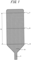
- FIG. 1 is a schematic diagram of the GaAs ingot obtained according to the production method of this disclosure.
- the GaAs ingot has a straight body portion 18 having an approximate identical diameter via a region 19 (also referred to as a cone portion) that increases in diameter from a seed crystal 6.
- FIG. 1 illustrates a position 16, which is the midpoint (50%) between the position 15 and the position 17.
- the percent of the position of each wafer from the seed side of the straight body portion is also referred to as a "position from the straight body seed”.
- Respective measurement values of the silicon (Si) concentration, the indium (In) concentration, the boron (B) concentration, the carrier concentration, the average dislocation density, the maximum dislocation density, the proportion of the area of a region with zero dislocation density to the wafer surface, and the absorption coefficient at a wavelength of 940 nm of the GaAs wafer and the GaAs wafer group according to this disclosure can be obtained by performing the measurement on a wafer obtained from the straight body portion 18 of the GaAs ingot.
- the size of the wafer according to this disclosure is a wafer size determined in the SEMI standard.
- the size of the wafer can be selected as appropriate from the diameter of the straight body portion 18 of the GaAs ingot.
- the size of the wafer can be, for example, 2 inches (diameter: 50 mm ⁇ 0.1 mm) or more and is preferably 3 inches (diameter: 76 mm ⁇ 0.1 mm) or more. From the point of the appropriateness for surface-emitting laser application, the size of the wafer is preferably 6 inches (diameter: 150 mm ⁇ 0.1 mm) or more. No specific limitations are placed on the upper limit of the wafer size.
- the wafer size can be, for example, 8 inches (diameter: 200 mm ⁇ 0.1 mm) or less.
- the evaluation at the seed side, the center portion, and the tail side of the GaAs ingot can be performed on wafers cut out from the respective ranges.
- any of upper and lower two surfaces of the wafer can be used.
- the following describes methods of measuring respective measurement values of the carrier concentration, the average dislocation density, the maximum dislocation density, the proportion of the area of a region with zero dislocation density to the wafer surface, the absorption coefficient, as well as the Si concentration, the In concentration, and the B concentration.
- the carrier concentration is a value measured by the Hall measurement using the Van der Pauw method after breaking out a fraction with a size of 10 mm ⁇ 10 mm at the wafer center portion from the extracted wafer and putting indium electrodes to its four corners to heat the fraction to 330 to 360°C.
- the average dislocation density is obtained by the measurement of a etch pit density (EPD).
- the measurement objects are etch pits that have hexagon-like shapes specific to zinc blende type crystals and have a major axis (length of diagonal passing through the center) of 20 ⁇ m or more.
- the measurement of the etch pit density is performed by setting 69 or 37 areas with a diameter of 3 mm on the wafer, observing each area with a microscope, and counting the number of the generated etch pits.
- the 69 or 37 areas are evenly distributed over the whole wafer surface.
- 69 areas are set at positions equally dispersed at intervals of 15 mm.
- 37 areas are set at positions equally dispersed at intervals of 10 mm.
- the interval of each area is 5 mm in a case of a 2-inch wafer, 10 mm in a case of a 4-inch wafer, and 20 mm in a case of an 8-inch wafer.
- FIG. 2 illustrates a schematic diagram of a 6-inch wafer in which 69 areas are set.
- a 10x objective lens with a field of view diameter of 1.73 mm is used for the observation of each area.
- the field of view in which the greatest number of pits are observed is searched in each area to count the number of the etch pits, and the number of etch pit counts is converted into a value per unit area (cm -2 ).
- the value obtaining by averaging the converted values of the numbers of etch pit counts in the respective areas is an average dislocation density.
- the measurement objects are etch pits that have hexagon-like shapes specific to zinc blende type crystals and have a major axis (length of diagonal passing through the center) of 20 ⁇ m or more.
- the proportion of the area of a region with zero dislocation density to the wafer surface is determined by generating etch pits in the same way as the above and measuring the distribution of these etch pits.
- a region excluding a toric part with a width of 3 mm from the outer periphery toward the center of the wafer surface from the whole wafer surface is divided into areas of 1 mm square, and each area is observed with a microscope using a 10x objective lens to count the number of etch pits in each area.
- the outer peripheral line of the region excluding a toric part with a width of 3 mm overlaps the areas of 1 mm squares (the outer peripheral line crosses the 1 mm squares)
- the outer peripheral line crosses the 1 mm squares when the area that falls within the measurement region within the outer peripheral line of a 1 mm square is large, the total area of this 1 mm square is measured, while the area that falls within the measurement region within the outer peripheral line of a 1 mm square is small, the total area of this 1 mm square is not measured, so that the area surrounded by the 1 mm squares with respect to the area surrounded by the outer peripheral line has an error within ⁇ 2% (preferably, an error within ⁇ 1.5%).
- the effective number of the areas of 1 mm squares to be measured at the whole wafer surface can be 3881 in the case of a 3-inch wafer (diameter: 76 mm), 6849 in the case of a 4-inch wafer (diameter: 100 mm), and 16529 in the case of a 6-inch wafer (diameter: 150 mm).
- the number of etch pits in each area may be counted by taking picture of each area using a camera equipped with a 10x objective lens.
- the proportion of the number of areas where the number of etch pits is 0 to the total number of areas is the proportion of the area of a region with zero dislocation density to the wafer surface.
- the greatest number of counts of the numbers of etch pit counts in the respective areas is the maximum dislocation density (mm -2 ).
- both of the back surface and the front surface of the extracted wafer is mirror finished to be a damage free state.
- the absorption coefficient is a value obtained by performing transmittance measurement with a spectrophotometer (UH5700 produced by Hitachi High-Tech Science Corporation) using a sample cut out with a size of 20 mm ⁇ 20 mm from around the center of the GaAs wafer that has been mirror finished in such a manner and whose thickness after finishing has been measured.
- the measurement conditions are as described below:
- I 0 is a light intensity before incidence
- I is a light intensity after wafer transmission
- T is a transmittance
- R is a reflectance
- ⁇ is an absorption coefficient
- d is a wafer thickness
- n is a wafer refractive index.
- the wafer is measured to a depth of 0.5 to 1 ⁇ m from the surface by setting the ion energy to 14.5 keV by the SIMS analysis with cesium ions.
- the wafer is measured to a depth of 3 ⁇ m from the surface by setting the ion energy to 5.5 keV by the SIMS analysis with oxygen ions.
- the following describes a method of producing a GaAs ingot according to this disclosure.
- this production method by the vertical gradient freezing (VGF) method or the vertical Bridgman (VB) method, using silicon (Si) and indium (In) as dopants, and using boric oxide (B 2 O 3 ) as a sealant, boric oxide (B 2 O 3 ) is stirred to lower the silicon concentration at the center portion of the GaAs ingot than the silicon concentration at the seed side to cause crystal growth.
- VVF vertical gradient freezing
- VB vertical Bridgman
- In is further added as a dopant in addition to Si to achieve low dislocation density of the GaAs ingot to be obtained.
- the crystal growth advances such that the solid-liquid interface moves from the edge at the seed crystal side toward the edge at the opposite side.
- the condensation of Si into a GaAs melt occurs by segregation (segregation coefficient of Si into GaAs (0.14)) to increase the Si concentration toward the tail side. Suppressing the increase in Si concentration associated with the crystal growth to lower the Si concentration at the center portion of the GaAs ingot than the Si concentration at the seed side is advantageous to increase the proportion of the area of a region with zero dislocation density.
- the Si concentration is controlled as describe below.
- Si is dissolved in the GaAs melt, and the following reaction occurs at the interface with B 2 O 3 .
- B 2 O 3 In the method of producing a GaAs ingot according to this disclosure, by stirring B 2 O 3 during the crystal growth, B 2 O 3 with a small content of Si is supplied to the interface with the melt to facilitate the reaction between B 2 O 3 and Si in the melt, which advances the above reaction to the right side to suppress the increase in Si concentration. At this time, the stirring is performed so that the Si concentration at the center portion of the GaAs ingot is lower than the Si concentration at the seed side.
- the crystal growth is performed from the seed to the cone portion in a state where a large amount of Si has been preliminarily contained in the melt, and from the crystal growth of the straight body portion, Si in the melt is incorporated into B 2 O 3 efficiently in large amounts to prevent the Si concentration from increasing due to the segregation of Si. In this manner, it is possible to obtain a wafer with suppressed carrier concentration and low dislocation density, as well as a large proportion of the area of a region with zero dislocation density to the GaAs wafer surface. By incorporating a large amount of Si in the melt into B 2 O 3 , a large amount of B is supplied into the melt.
- the activation rate of silicon added as a dopant can be reduced, which can control the carrier concentration and thus the absorption coefficient.
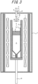
- FIG. 3 schematically illustrates a cross-sectional view of an example of a production device used in the method of producing a GaAs ingot according to this disclosure.
- the production device illustrated in FIG. 3 includes an air tight container 7 that can be evacuated and filled with atmosphere gas from the outside, a crucible 3 arranged at the center in the air tight container 7, a crucible housing container (susceptor) 2 that houses and holds the crucible 3, a mechanism 14 that moves up and down and/or rotates the crucible housing container (susceptor) 2 (only an up-and-down and rotating rod is illustrated), and a heater 1 mounted to surround the crucible housing container (susceptor) 2 in the air tight container 7.
- the stirring blade 20 and the upper rod 21 form a stirring means.
- the stirring blade 20 can be removed from the upper rod 21.
- a sealant housing container and other members can be attached to the upper rod 21.
- the crucible 3 can be formed of pyrolytic boron nitride (PBN).
- PBN pyrolytic boron nitride
- the crucible 3 is filled with the seed crystal 6, compound semiconductor raw materials 5, and a sealant (B 2 O 3 ) 4, and the air tight container 7 is filled with an inert gas 8 as an example.
- FIG. 4 schematically illustrates a cross-sectional view of an example of a crucible used in the method of producing a GaAs ingot according to this disclosure and corresponds to a state where the crucible is filled with raw materials, etc. before the start of crystal growth.
- the crucible 3 illustrated in FIG. 4 is filled with the seed crystal 6, GaAs polycrystalline raw materials 9, a dopant (silicon) 10, a dopant (indium) 11, and a sealant (B 2 O 3 ) 4.
- the GaAs polycrystalline raw materials 9 are arranged as crushed GaAs polycrystals (9A), cylindrical GaAs polycrystal containers (9B), and disk GaAs polycrystals (9C).
- the GaAs polycrystalline raw materials 9 are not limited to such an aspect. For example, only crushed GaAs polycrystals may be arranged.
- the temperature of the GaAs polycrystalline raw materials 9 is increased to the melting point of GaAs, 1238°C, or more, while applying a temperature gradient by a PID controlled heater to decrease the temperature at the side of the seed crystal 6, to prevent the seed crystal 6 from melting.
- the GaAs polycrystalline raw materials 9 and the sealant (B 2 O 3 ) 4 are melted to dissolve the dopant (silicon) and the dopant (indium) 11 in the GaAs melt.
- the rate of temperature decrease is preferably 10°C/h or less.
- the sealant (B 2 O 3 ) 4 is stirred during the crystal growth.
- the stirring is performed so that the Si concentration at the center portion of the GaAs ingot is lower than the Si concentration at the seed side. It is preferable to start the stirring between the time point at which the crystal growth starts at the seed side of the straight body portion and the time point at which the crystal growth reaches the center portion (position from the straight body seed: 1 to 40%). It is more preferable to start the stirring at the time point with a position from the straight body seed of 1 to 20%. The stirring may be started prior to this time point.
- the stirring may be started in the middle of the cone portion or at the time point at which the crystal growth starts at a part where the cone portion is switched to the straight body portion (position from the straight body seed: around 0%).
- the stirring preferably continues until the crystal growth at the tail side of the straight body portion ends and may be continue until the crystal growth ends.
- the stirring is preferably performed by arranging and rotating the stirring means in the sealant (B 2 O 3 ) 4.
- the number of rotations is preferably adjusted by gradually increasing it from a small number so as to moderately adjust the change in Si concentration.
- the number of rotations may be changed stepwise or changed continuously.
- the maximum number of rotations to reach is preferably 6 rpm or more, and more preferably 10 rpm or more, from the point of reaction promotion.
- the number of rotations can be, for example, 20 rpm or less.
- the stirring means may have a form where the stirring blade is attached to around the rotation shaft.
- the stirring blade can be formed of a plate member with a predetermined shape and is, for example, formed of two to eight approximately quadrangular plate members. As its material, carbon, BN, etc. are used.
- the plate member is preferably attached with an angle of gradient of 45° or more and 135° or less with respect to the interface formed by the GaAs melt and B 2 O 3 in a resting state.
- the area formed by the rotation locus when the stirring means is rotated is preferably 30% or more, and more preferably 70% or more of the area of the interface formed by the GaAs melt and B 2 O 3 in the resting state.
- the distance between the lower end of the stirring blade and the interface formed by the GaAs melt and B 2 O 3 in the resting state is preferably less than 2 mm, and preferably 1 mm or less. However, it is preferable to prevent the lower end of the stirring blade from contacting the interface.
- the seed crystal 6 may have a cross-sectional area of, for example, 1 to 20% and preferably have a cross-sectional area of 3 to 17% with respect to the cross-sectional area having a diameter that is the inner diameter of the crucible 3.
- the cross-sectional area of the seed crystal 6 can be 2 to 10% with respect to the cross-sectional area having a diameter that is the crucible inner diameter.
- the inner diameter of the crucible 3 is preferably slightly larger than the aimed wafer size.
- the aimed wafer size can be, for example, 2 inches or more and is preferably 3 inches or more, and further preferably 6 inches or more. No specific limitations are placed on the upper limit of the wafer size.
- the upper limit of the wafer size can be, for example, 8 inches or less.
- Silicon (Si) and indium (In) are used as dopants.
- the dopant (silicon) 10 is added to the GaAs polycrystalline raw materials 9, with a weight to achieve a desired concentration by the shot of high purity Si or by crushing a high purity Si substrate.
- the dopant (indium) 11 is also added to the GaAs polycrystalline raw materials 9, with a weight to achieve a desired concentration using high purity In, indium compound (e.g., high purity indium arsenide (InAs)).
- the silicon charge amount is preferably equal to or more than the amount used for producing a normal silicon doped GaAs ingot.
- the silicon charge amount can be, for example, 110 wtppm or more and 150 wtppm or less and is preferably 120 wtppm or more and 140 wtppm or less, and more preferably 130 wtppm or more and 140 wtppm or less, with respect to GaAs polycrystalline raw materials.
- the silicon charge amount does not include the amount of silicon contained in B 2 O 3 .
- the silicon charge amount can be an amount to have a silicon concentration at the seed side of the straight body portion of 7.0 ⁇ 10 17 cm -3 or more, when a GaAs ingot is produced under the same conditions except that B 2 O 3 is not stirred.
- a large diameter of 4 inches or more such as 6 inches
- the indium charge amount can be 100 wtppm or more and 5000 wtppm or less and is preferably 500 wtppm or more and 4000 wtppm or less, and more preferably 1000 wtppm or more and 2000 wtppm or less, with respect to the GaAs polycrystalline raw materials.
- InAs indium arsenide
- the indium charge amount may be converted from the charge amount of InAs raw materials.
- the melting point of In is 156°C, and the melting point of InAs is 942°C. Thus, these melting points are significantly lower than the melting point of GaAs, 1238°C.
- any measures are necessary to prevent the previously melted In from easily adhering to around the seed crystal 6, such as putting the dopant (indium) 11 into a position away from the seed crystal 6 or devising the arrangement of the GaAs polycrystalline raw materials 9.
- FIG. 4 illustrates an example of the aspect.
- the dopant (indium) 11 is arranged above the center of the crucible (position corresponding to the center portion of the ingot).
- the dopant (indium) 11 is put into a container (GaAs container) produced from GaAs crystal or GaAs polycrystal, so that the dopant inside does not come out of the container until the temperature at which the GaAs container melts.
- the dopant (silicon) 10 is preferably arranged below the center of the crucible (position corresponding to the center portion of the ingot) (seed crystal side).
- the dopant (silicon) 10 may be put into the GaAs container, so that the dopant inside does not come out of the container until the temperature at which the GaAs container melts. Silicon has a density lower than that of GaAs.
- the dopant (silicon) floats upward in the melt, and the silicon concentration in the GaAs melt at the seed crystal side decreases, which may decrease the silicon concentration at the seed side of the GaAs ingot.
- the use of the GaAs container is effective to avoid such matters.
- the size of the seed crystal 6 is preferably within the above range also for preventing In from easily adhering to around the seed crystal 6.
- Elements conceivable as dopants other than silicon and indium include beryllium (Be), magnesium (Mg), aluminum (Al), carbon (C), germanium (Ge), tin (Sn), nitrogen (N), sulfur (S), selenium (Se), and tellurium (Te) and further include zinc (Zn), cadmium (Cd), chromium (Cr), and antimony (Sb).
- Be beryllium
- Mg magnesium
- Al aluminum
- C germanium
- Ge germanium
- tin (Sn) nitrogen
- N sulfur
- S selenium
- Te tellurium
- Zn zinc
- Cd cadmium
- Cr chromium
- Sb antimony
- the sealant (B 2 O 3 ) 4 for the reaction promotion with silicon a sealant (B 2 O 3 ) with reduced content of silicon is preferably used.
- the silicon concentration in B 2 O 3 can be 2 mol% or less, is preferably 1 mol% or less, and may be 0 mol%. A smaller silicon concentration in B 2 O 3 tends to decrease the activation rate.
- the silicon concentration in B 2 O 3 it is possible to obtain more wafers with a large proportion of the area of a region with zero dislocation density to the GaAs wafer surface, from the ingot.
- Silicon may be contained in B 2 O 3 in a form of Si oxide.
- the method of producing a GaAs ingot at at least any position of the seed side, the center portion, and the tail side of the GaAs ingot, it is possible to have a part having a silicon concentration of 1.0 ⁇ 10 17 cm -3 or more and less than 1.1 ⁇ 10 18 cm -3 , an indium concentration of 3.0 ⁇ 10 18 cm -3 or more and less than 3.0 ⁇ 10 19 cm -3 , and a boron concentration of 2.5 ⁇ 10 18 cm -3 or more, having a carrier concentration of 1.0 ⁇ 10 16 cm -3 or more and 4.0 ⁇ 10 17 cm -3 or less, and having a region with zero dislocation density to the wafer surface of 91.0% or more.
- At least the center portion of the straight body portion has such a part. It is more preferable that all of the seed side, the center portion, and the tail side of the straight body portion each have such a part.
- this part can have an average dislocation density of 250 cm -2 or less and can have an absorption coefficient at a wavelength of 940 nm of 3.5 cm -1 or more and 7.0 cm -1 or less.
- the GaAs wafer according to this disclosure can be obtained by cutting out a wafer from at least any position of the seed side, the center portion, and the tail side of the GaAs ingot obtained by the method of producing a GaAs ingot according to this disclosure.
- the GaAs wafer according to this disclosure can be preferably obtained from the center portion and can be further preferably obtained from all of the seed side, the center portion, and the tail side.
- the GaAs wafer according to this disclosure has a silicon concentration of 1.0 ⁇ 10 17 cm -3 or more and less than 1.1 ⁇ 10 18 cm -3 , an indium concentration of 3.0 ⁇ 10 18 cm -3 or more and less than 3.0 ⁇ 10 19 cm -3 , and a boron concentration of 2.5 ⁇ 10 18 cm -3 or more, has a carrier concentration of 1.0 ⁇ 10 16 cm -3 or more and 4.0 ⁇ 10 17 cm -3 or less, and has a region with zero dislocation density to the wafer surface of 91.0% or more.
- This GaAs wafer can have an average dislocation density of 250 cm -2 or less and can have an absorption coefficient at a wavelength of 940 nm of 3.5 cm -1 or more and 7.0 cm -1 or less.
- the following describes the ranges of the Si concentration, the In concentration, the B concentration, the average dislocation density, the maximum dislocation density, the proportion of the area of a region with zero dislocation density to the wafer surface, the carrier concentration, the absorption coefficient, etc. of the GaAs wafer according to this disclosure.
- the Si concentration of the GaAs wafer according to this disclosure is 1.0 ⁇ 10 17 cm -3 or more and less than 1.1 ⁇ 10 18 cm -3 .
- the In concentration of the GaAs wafer according to this disclosure is 3.0 ⁇ 10 18 cm -3 or more and less than 3.0 ⁇ 10 19 cm -3 .
- the GaAs wafer according to this disclosure can be advantageously obtained by the reaction promotion between the sealant (B 2 O 3 ) and Si as a dopant, in the crystal growth of the GaAs ingot by the VGF method or the VB method.
- the B concentration is 2.5 ⁇ 10 18 cm -3 or more, and the B concentration is preferably 3.0 ⁇ 10 18 cm -3 or more. No specific limitations are placed on the upper limit of the B concentration. However, the B concentration can be 3.0 ⁇ 10 19 cm -3 or less.
- elements other than Si and In are not added, other than GaAs, except for B and oxygen (O) mixed in the GaAs ingot by B 2 O 3 used as the sealant. Only Si and In are added as dopants, and it is preferable that the other elements are not intentionally added as dopants.
- Elements conceivable as dopants other than silicon and indium include beryllium (Be), magnesium (Mg), aluminum (Al), carbon (C), germanium (Ge), tin (Sn), nitrogen (N), sulfur (S), selenium (Se), and tellurium (Te) and further include zinc (Zn), cadmium (Cd), chromium (Cr), and antimony (Sb).
- Be beryllium
- Mg magnesium
- Al aluminum
- C germanium
- Ge germanium
- tin (Sn) nitrogen
- N sulfur
- S selenium
- Te tellurium
- Zn zinc
- Cd cadmium
- Cr chromium
- Sb antimony
- each concentration of Al, C, and Zn in GaAs by the SIMS analysis is preferably 3 ⁇ 10 16 cm -3 or less (including zero).
- Each concentration of Be, Mg, Ge, Sn, N, S, Se, Te, Cd, Cr, and Sb other than these elements is preferably 5 ⁇ 10 15 cm -3 or less (including zero).
- the concentration of N is more preferably 1 ⁇ 10 15 cm -3 or less.
- the value of the average dislocation density of the GaAs wafer according to this disclosure is preferably 250 cm -2 or less. No specific limitations are placed on the lower limit of the average dislocation density. When the average dislocation density is 10 cm -2 or more, in particular, 30 cm -2 or more, the effect of specifying the proportion of the area a region with zero dislocation density is effectively provided.
- the GaAs wafer according to this disclosure has a proportion of the area of a region with zero dislocation density to the wafer surface of 91.0% or more.
- the proportion of the area of a region with zero dislocation density to the wafer surface may be 100%.
- the GaAs wafer according to this disclosure has a carrier concentration of 1.0 ⁇ 10 16 cm -3 or more and 4.0 ⁇ 10 17 cm -3 or less.
- the absorption coefficient at a wavelength of 940 nm is preferably 3. 5 cm -1 or more and 7.0 cm -1 or less.
- the GaAs wafer group according to this disclosure can be obtained by cutting out a plurality of wafers from at least any position of the seed side, the center portion, and the tail side of the GaAs ingot obtained by the method of producing a GaAs ingot according to this disclosure.
- the GaAs wafer group according to this disclosure can be preferably obtained from the center portion and can be further preferably obtained from all of the seed side, the center portion, and the tail side.
- the GaAs wafer group according to this disclosure is consist of a plurality of wafers obtained from an identical ingot. No specific limitations are placed on the number of the plurality of wafers so long as the number is 2 or more. However, the plurality of wafers are preferably half or more of the total number of wafers that can be cut out from an identical ingot, more preferably the total number of wafers obtained from the center portion of an identical ingot, and further preferably the total number of wafers obtained from the seed side to the tail side of an identical ingot. The plurality of wafers are particularly preferably the total number of wafers obtained between the edge at the seed crystal side of the seed side and the edge opposite to the seed crystal of the tail side.
- Each of the plurality of wafers has a silicon concentration of 1.0 ⁇ 10 17 cm -3 or more and less than 1.1 ⁇ 10 18 cm -3 , an indium concentration of 3.0 ⁇ 10 18 cm -3 or more and less than 3.0 ⁇ 10 19 cm -3 , and a boron concentration of 2.5 ⁇ 10 18 cm -3 or more, has a carrier concentration of 1.0 ⁇ 10 16 cm -3 or more and 4.0 ⁇ 10 17 cm -3 or less, and has a region with zero dislocation density to the wafer surface of 91.0% or more.
- This GaAs wafer can have an average dislocation density of 250 cm -2 or less and can have an absorption coefficient at a wavelength of 940 nm of 3.5 cm -1 or more and 7.0 cm -1 or less. These preferred ranges are as described for the GaAs wafer according to this disclosure.
- the plurality of wafers include a wafer obtained from the center portion of the straight body portion of the GaAs ingot and that the wafer obtained from the center portion further has a carrier concentration of less than 2.0 ⁇ 10 17 cm -3 .
- the carrier concentration of the wafer obtained from the center portion can be 1.0 ⁇ 10 16 cm -3 or more.
- the GaAs wafer according to this disclosure has suppressed carrier concentration and low dislocation density, as well as a large proportion of the area of a region with zero dislocation density to the GaAs wafer surface, and thus is suitable for the substrate of the surface-emitting laser including a vertical cavity surface-emitting laser (VCSEL).
- VCSEL vertical cavity surface-emitting laser
- a GaAs ingot was produced using a production device having a configuration illustrated in FIG. 3 .
- the stirring blade is formed by attaching four quadrangular plate members with a material having no effect on the crystal characteristics, such as carbon and BN, to the rod.
- the area formed by the rotation locus when the stirring blade rotates is 50% or more of the area of the interface formed by the GaAs melt and B 2 O 3 in the resting state.
- the crucible 3 formed of PBN with an inner diameter of 159.9 mm and the inner diameter of the seed portion of 6.0 to 6.5 mm was prepared as a crucible.
- the crucible was filled with the GaAs polycrystalline raw materials 9A of 20,000 ⁇ 10 g, which were obtained by crushing GaAs polycrystal formed by synthesizing Ga of 6N (purity: 99.9999% or more) and As of 6N, and the GaAs seed crystal 6, which was cut out such that a (100) surface is a crystal growth surface, as illustrated in FIG. 4 .
- the diameter of the GaAs seed crystal 6 was adjusted by a combination of machine grinding and etching so that it is smaller than the inner diameter of the seed portion of each crucible by about 0.5 mm.
- the crucible was filled with high purity Si shot of 100 wtppm as the dopant (silicon) 10 and high purity InAs shot of 2000 wtppm (In equivalent: 1210 wtppm) as the dopant (indium) 11, with respect to the GaAs polycrystalline raw materials. No impurity elements were intentionally added other than Si and In.
- the crucible was filled with the granular dopant (silicon) 10 and dopant (indium) 11, which were each in a state contained in a GaAs container formed by sandwiching a cylindrical GaAs polycrystal 9B between disk GaAs polycrystals 9C from up and down, so that the dopant inside does not come out of the GaAs container until the temperature at which the GaAs container melts.
- the dopant (indium) 11 was arranged above the center of the crucible 3, while the dopant (silicon) 10 was arranged near the seed crystal 6 under the center of the crucible 3.
- the crucible was filled with these raw materials, the crucible was filled with the sealant, B 2 O 3 (Si concentration: 5 mol%) 4 of 965 ⁇ 10g.
- the crucible 3 after the filling was set in the crucible housing container (susceptor). After the inside of the production device illustrated in FIG. 3 was repeatedly evacuated and substituted by Ar gas to make an inert gas atmosphere, single crystal was grown by the VGF method.
- the temperature of the raw materials in the crucible was increased to the melting point of GaAs, 1238°C, or more to prepare a melt, while applying a temperature gradient by a PID controlled heater to decrease the temperature at the seed crystal side, to prevent the GaAs seed crystal from melting. Then, after increasing the temperature around the seed crystal to melt the upper portion of the seed crystal, the temperature of the entire furnace was decreased at a rate of 10°C/h or less by heater control while applying the temperature gradient, which grew an n-type GaAs ingot with Si as a dopant.
- the stirring blade was rotated to start the stirring of B 2 O 3 , such that the distance between the interface between the sealant, B 2 O 3 , and the crystal tail side, and the lower end of the stirring blade was 3 mm or less and the lower end did not contact the interface.
- the rotation rate of the stirring blade is increase stepwise from a small number of rotations to 10 rpm, and the stirring was continued at 10 rpm by the completion of growth of the tail side.
- the number of rotations of the stirring blade was adjusted as the number of rotations increases stepwise, so that the number of rotations is 5 rpm from the position of 25 mm from the place where the cone portion underwent the crystal growth to reach the crystal straight body portion to the straight body portion side (position from the straight body seed: 16%) to the position of 50 mm, 7.6 rpm from the position of 50 mm (position from the straight body seed: 30%) to the position of 100 mm, and 10 rpm after the position of 100 mm (position from the straight body seed: 61%).
- the straight body portion of the grown GaAs ingot was sliced with a wire-saw to form a wafer.
- the wafer size corresponds to 6 inches.
- the last cutting surface was at a position of 20 mm from the edge at the side opposite to the seed crystal side of the ingot (in the seed side direction).
- the evaluation was performed on each wafer obtained at the seed side, the center portion, and the tail side of the straight body portion of the GaAs ingot, and each wafer obtained between the seed side and the center portion and between the center portion and the tail side.
- the Si concentration, the In concentration, and the B concentration were measured by the SIMS analysis using a device produced by CAMECA.
- the number of etch pits was counted as described above on the surface of the wafer adjacent to (opposite to via an identical cutting surface) the above wafer used for the Hall measurement, and the number of counts was evaluated as an average dislocation density (cm -2 ).
- the counting was performed by changing the 10x objective lens to a 5x objective lens with a field of view diameter of 3.46 mm.
- the proportion of the area of a region with zero dislocation density to the wafer surface, and the maximum dislocation density were determined as described above, using a wafer near the wafer used for the Hall measurement or the EPD measurement.
- the absorption coefficient at a wavelength of 920 nm was measured, using a wafer near the wafer used for the Hall measurement or the EPD measurement.
- the transmittance was measured using a spectrophotometer (UH5700 produced by Hitachi High-Tech Science Corporation), and the absorption coefficient was determined further using the aforementioned formulas [1] and [2].
- An GaAs ingot was grown in the same manner as in Crystal number 1, using a production device for 3-inch wafer.
- High purity Si shot of 130 wtppm as a dopant (silicon) and high purity InAs shot of 2000 wtppm (In equivalent: 1210 wtppm) were used with respect to the GaAs polycrystalline raw materials.
- a wafer was obtained and evaluated in the same manner as in Crystal number 1, except that the straight body portion of the grown GaAs ingot was slice with a wire-saw to form a wafer corresponding to 3 inches.
- a GaAs ingot of Crystal number 8 was produced in the same manner as in Crystal number 6, except that the number of rotations of the stirring blade was adjusted as the number of rotations increases stepwise, so that the number of rotations is 5 rpm from the position of 12.5 mm from the place where the cone portion underwent the crystal growth to reach the crystal straight body portion to the straight body portion side (position from the straight body seed: 8%) to the position of 50 mm, 7.6 rpm from the position of 50 mm to the position of 100 mm, and 10 rpm after the position of 100 mm. Then, a wafer was obtained and evaluated.
- a GaAs ingot of Crystal number 9 was produced and evaluated in the same manner as in Crystal number 8, except that the Si charge amount was changed from 140 wtppm to 130 wtppm, and the Si concentration in B 2 O 3 was changed from 0 mol% to 0.25 mol%, as in the condition presented in Table 1.
- the conductivity type of the obtained GaAs ingots is n-type. From Crystal numbers 2 to 9 that underwnet crystal growth by stirring boric oxide so that the silicon concentration at the centre portion of the straight body portion was lower than the silicon concentration at the seed side of the straight body portion of the GaAs ingot, a plurality of wafers having a silicon concentration of 1.0 ⁇ 10 17 cm -3 or more and less than 1.1 ⁇ 10 18 cm -3 , an indium concentration of 3.0 ⁇ 10 18 cm -3 or more and less than 3.0 ⁇ 10 19 cm -3 , and a boron concentration of 2.5 ⁇ 10 18 cm -3 or more, having a carrier concentration of 1.0 ⁇ 10 16 cm -3 or more and 4.0 ⁇ 10 17 cm -3 or less, and having a proportion of the area of a region with zero dislocation density to the wafer surface of 91.0% or more could be obtained from at least a part of the GaAs ingot.
- a GaAs wafer and a GaAs wafer group that have suppressed carrier concentration and low dislocation density, as well as a large proportion of the area of a region with zero dislocation density to the GaAs wafer surface, and thus are suitable for the substrate of the surface-emitting laser including a vertical cavity surface-emitting laser (VCSEL).
- VCSEL vertical cavity surface-emitting laser
Landscapes
- Chemical & Material Sciences (AREA)
- Engineering & Computer Science (AREA)
- Crystallography & Structural Chemistry (AREA)
- Materials Engineering (AREA)
- Metallurgy (AREA)
- Organic Chemistry (AREA)
- Inorganic Chemistry (AREA)
- Crystals, And After-Treatments Of Crystals (AREA)
Applications Claiming Priority (3)
| Application Number | Priority Date | Filing Date | Title |
|---|---|---|---|
| JP2021159962 | 2021-09-29 | ||
| JP2022150699A JP7256326B1 (ja) | 2021-09-29 | 2022-09-21 | GaAsウエハ、GaAsウエハ群及びGaAsインゴットの製造方法 |
| PCT/JP2022/035510 WO2023054202A1 (ja) | 2021-09-29 | 2022-09-22 | GaAsウエハ、GaAsウエハ群及びGaAsインゴットの製造方法 |
Publications (2)
| Publication Number | Publication Date |
|---|---|
| EP4411031A1 true EP4411031A1 (de) | 2024-08-07 |
| EP4411031A4 EP4411031A4 (de) | 2025-10-22 |
Family
ID=85782622
Family Applications (1)
| Application Number | Title | Priority Date | Filing Date |
|---|---|---|---|
| EP22876069.0A Pending EP4411031A4 (de) | 2021-09-29 | 2022-09-22 | Gaas wafer, gaas wafer gruppe und verfahren zur herstellung eines gaas blocks |
Country Status (4)
| Country | Link |
|---|---|
| US (1) | US20240392475A1 (de) |
| EP (1) | EP4411031A4 (de) |
| TW (1) | TWI824748B (de) |
| WO (1) | WO2023054202A1 (de) |
Family Cites Families (8)
| Publication number | Priority date | Publication date | Assignee | Title |
|---|---|---|---|---|
| JPS649898A (en) * | 1987-07-02 | 1989-01-13 | Nippon Mining Co | Production of silicon-containing gaas single crystal |
| JP2003206200A (ja) * | 2002-01-10 | 2003-07-22 | Hitachi Cable Ltd | p型GaAs単結晶及びその製造方法 |
| US7175707B2 (en) * | 2003-03-24 | 2007-02-13 | Hitachi Cable Ltd. | P-type GaAs single crystal and its production method |
| JP2007210882A (ja) * | 2007-02-05 | 2007-08-23 | Dowa Holdings Co Ltd | SiドープGaAs単結晶並びにその製造方法 |
| US8361225B2 (en) * | 2007-05-09 | 2013-01-29 | Axt, Inc. | Low etch pit density (EPD) semi-insulating III-V wafers |
| JP5433632B2 (ja) * | 2011-05-25 | 2014-03-05 | Dowaエレクトロニクス株式会社 | GaAs単結晶の製造方法およびGaAs単結晶ウェハ |
| DE102019208389A1 (de) * | 2019-06-07 | 2020-12-10 | Freiberger Compound Materials Gmbh | Verfahren zur Herstellung von Restspannungs- und versetzungsfreien AIII-BV-Substratwafern |
| EP4166698A4 (de) * | 2020-06-12 | 2024-06-05 | DOWA Electronics Materials Co., Ltd. | Gaas-ingot, verfahren zur herstellung eines gaas-ingots und gaas-wafer |
-
2022
- 2022-09-22 EP EP22876069.0A patent/EP4411031A4/de active Pending
- 2022-09-22 US US18/687,812 patent/US20240392475A1/en active Pending
- 2022-09-22 WO PCT/JP2022/035510 patent/WO2023054202A1/ja not_active Ceased
- 2022-09-28 TW TW111136817A patent/TWI824748B/zh active
Also Published As
| Publication number | Publication date |
|---|---|
| TW202314070A (zh) | 2023-04-01 |
| TWI824748B (zh) | 2023-12-01 |
| WO2023054202A1 (ja) | 2023-04-06 |
| US20240392475A1 (en) | 2024-11-28 |
| EP4411031A4 (de) | 2025-10-22 |
Similar Documents
| Publication | Publication Date | Title |
|---|---|---|
| Kasap et al. | Mercury cadmium telluride: growth, properties and applications | |
| TWI778658B (zh) | GaAs錠及GaAs錠的製造方法以及GaAs晶圓 | |
| MacKenzie et al. | Advancements in THM-grown CdZnTe for use as substrates for HgCdTe | |
| EP3591102A1 (de) | Verbindungshalbleiter und verfahren zur herstellung eines einkristalls eines verbindungshalbleiters | |
| EP0092409B1 (de) | Verfahren zur Herstellung eines mit Bor dotierten Galliumarsenid Monokristalls | |
| US4196171A (en) | Apparatus for making a single crystal of III-V compound semiconductive material | |
| Mühlberg et al. | Crystalline and chemical quality of CdTe and Cd1-xZnxTe grown by the Bridgman method in low temperature gradients | |
| CN110202419B (zh) | 锗单晶片、其制法、晶棒的制法及单晶片的用途 | |
| EP4411031A1 (de) | Gaas wafer, gaas wafer gruppe und verfahren zur herstellung eines gaas blocks | |
| JP7256326B1 (ja) | GaAsウエハ、GaAsウエハ群及びGaAsインゴットの製造方法 | |
| TWI795937B (zh) | n型GaAs晶圓和n型GaAs錠的製造方法 | |
| He et al. | Effect of temperature gradient on microstructure and properties of GaSb crystals grown with Bridgman method | |
| EP4592431A1 (de) | Verfahren zur herstellung eines gaas-ingots und gaas-ingot | |
| CN118043506A (zh) | GaAs晶圆、GaAs晶圆组和GaAs晶锭的制造方法 | |
| JP7576672B2 (ja) | GaAsインゴットの製造方法及びGaAsインゴット | |
| Reijnen et al. | Comparison Of LEC‐Grown And VGF‐Grown GaSb | |
| Bliss et al. | Growth and characterization of bulk GaInSb crystals from non-stoichiometric melts | |
| Azoulay et al. | Growth and characterization of CdTe and CdZnTe crystals for substrate application | |
| Li et al. | Growth and characterization of liquid-phase epitaxial Hg1− xCdxTe films | |
| Ciszek et al. | Effect of nitrogen doping on microdefects and minority charge carrier lifetime of high-purity, dislocation-free and multicrystalline silicon | |
| Chen | Jason MacKenzie, Francis Joseph Kumar | |
| Wei et al. | Electrical and Optical Characterization of Melt-Grown Bulk InAs1− y P y Crystals | |
| Capper | Use of forced mixing via the accelerated crucible rotation technique (ACRT) in Bridgman growth of cadmium mercury telluride (CMT) | |
| Nagashio et al. | Optical absorption issues in CdGeAs2 single crystals | |
| Mori et al. | High‐Rate Deposition of Amorphous Silicon Films by Atmospheric‐Pressure Plasma Chemical Vapor Deposition |
Legal Events
| Date | Code | Title | Description |
|---|---|---|---|
| STAA | Information on the status of an ep patent application or granted ep patent |
Free format text: STATUS: THE INTERNATIONAL PUBLICATION HAS BEEN MADE |
|
| PUAI | Public reference made under article 153(3) epc to a published international application that has entered the european phase |
Free format text: ORIGINAL CODE: 0009012 |
|
| STAA | Information on the status of an ep patent application or granted ep patent |
Free format text: STATUS: REQUEST FOR EXAMINATION WAS MADE |
|
| 17P | Request for examination filed |
Effective date: 20240314 |
|
| AK | Designated contracting states |
Kind code of ref document: A1 Designated state(s): AL AT BE BG CH CY CZ DE DK EE ES FI FR GB GR HR HU IE IS IT LI LT LU LV MC MK MT NL NO PL PT RO RS SE SI SK SM TR |
|
| DAV | Request for validation of the european patent (deleted) | ||
| DAX | Request for extension of the european patent (deleted) | ||
| A4 | Supplementary search report drawn up and despatched |
Effective date: 20250919 |
|
| RIC1 | Information provided on ipc code assigned before grant |
Ipc: C30B 29/42 20060101AFI20250915BHEP Ipc: C30B 29/40 20060101ALI20250915BHEP |