EP4408145A1 - Solar cell preparation method, solar cell and laminated solar cell - Google Patents
Solar cell preparation method, solar cell and laminated solar cell Download PDFInfo
- Publication number
- EP4408145A1 EP4408145A1 EP22957622.8A EP22957622A EP4408145A1 EP 4408145 A1 EP4408145 A1 EP 4408145A1 EP 22957622 A EP22957622 A EP 22957622A EP 4408145 A1 EP4408145 A1 EP 4408145A1
- Authority
- EP
- European Patent Office
- Prior art keywords
- layer
- perovskite
- monocrystal
- solar cell
- functional layer
- Prior art date
- Legal status (The legal status is an assumption and is not a legal conclusion. Google has not performed a legal analysis and makes no representation as to the accuracy of the status listed.)
- Granted
Links
Images





Classifications
-
- H—ELECTRICITY
- H10—SEMICONDUCTOR DEVICES; ELECTRIC SOLID-STATE DEVICES NOT OTHERWISE PROVIDED FOR
- H10K—ORGANIC ELECTRIC SOLID-STATE DEVICES
- H10K30/00—Organic devices sensitive to infrared radiation, light, electromagnetic radiation of shorter wavelength or corpuscular radiation
- H10K30/30—Organic devices sensitive to infrared radiation, light, electromagnetic radiation of shorter wavelength or corpuscular radiation comprising bulk heterojunctions, e.g. interpenetrating networks of donor and acceptor material domains
- H10K30/35—Organic devices sensitive to infrared radiation, light, electromagnetic radiation of shorter wavelength or corpuscular radiation comprising bulk heterojunctions, e.g. interpenetrating networks of donor and acceptor material domains comprising inorganic nanostructures, e.g. CdSe nanoparticles
-
- H—ELECTRICITY
- H10—SEMICONDUCTOR DEVICES; ELECTRIC SOLID-STATE DEVICES NOT OTHERWISE PROVIDED FOR
- H10F—INORGANIC SEMICONDUCTOR DEVICES SENSITIVE TO INFRARED RADIATION, LIGHT, ELECTROMAGNETIC RADIATION OF SHORTER WAVELENGTH OR CORPUSCULAR RADIATION
- H10F10/00—Individual photovoltaic cells, e.g. solar cells
- H10F10/10—Individual photovoltaic cells, e.g. solar cells having potential barriers
- H10F10/19—Photovoltaic cells having multiple potential barriers of different types, e.g. tandem cells having both PN and PIN junctions
-
- H—ELECTRICITY
- H10—SEMICONDUCTOR DEVICES; ELECTRIC SOLID-STATE DEVICES NOT OTHERWISE PROVIDED FOR
- H10F—INORGANIC SEMICONDUCTOR DEVICES SENSITIVE TO INFRARED RADIATION, LIGHT, ELECTROMAGNETIC RADIATION OF SHORTER WAVELENGTH OR CORPUSCULAR RADIATION
- H10F19/00—Integrated devices, or assemblies of multiple devices, comprising at least one photovoltaic cell covered by group H10F10/00, e.g. photovoltaic modules
- H10F19/40—Integrated devices, or assemblies of multiple devices, comprising at least one photovoltaic cell covered by group H10F10/00, e.g. photovoltaic modules comprising photovoltaic cells in a mechanically stacked configuration
-
- H—ELECTRICITY
- H10—SEMICONDUCTOR DEVICES; ELECTRIC SOLID-STATE DEVICES NOT OTHERWISE PROVIDED FOR
- H10K—ORGANIC ELECTRIC SOLID-STATE DEVICES
- H10K30/00—Organic devices sensitive to infrared radiation, light, electromagnetic radiation of shorter wavelength or corpuscular radiation
- H10K30/40—Organic devices sensitive to infrared radiation, light, electromagnetic radiation of shorter wavelength or corpuscular radiation comprising a p-i-n structure, e.g. having a perovskite absorber between p-type and n-type charge transport layers
-
- H—ELECTRICITY
- H10—SEMICONDUCTOR DEVICES; ELECTRIC SOLID-STATE DEVICES NOT OTHERWISE PROVIDED FOR
- H10K—ORGANIC ELECTRIC SOLID-STATE DEVICES
- H10K71/00—Manufacture or treatment specially adapted for the organic devices covered by this subclass
- H10K71/80—Manufacture or treatment specially adapted for the organic devices covered by this subclass using temporary substrates
-
- H—ELECTRICITY
- H10—SEMICONDUCTOR DEVICES; ELECTRIC SOLID-STATE DEVICES NOT OTHERWISE PROVIDED FOR
- H10K—ORGANIC ELECTRIC SOLID-STATE DEVICES
- H10K85/00—Organic materials used in the body or electrodes of devices covered by this subclass
- H10K85/50—Organic perovskites; Hybrid organic-inorganic perovskites [HOIP], e.g. CH3NH3PbI3
-
- Y—GENERAL TAGGING OF NEW TECHNOLOGICAL DEVELOPMENTS; GENERAL TAGGING OF CROSS-SECTIONAL TECHNOLOGIES SPANNING OVER SEVERAL SECTIONS OF THE IPC; TECHNICAL SUBJECTS COVERED BY FORMER USPC CROSS-REFERENCE ART COLLECTIONS [XRACs] AND DIGESTS
- Y02—TECHNOLOGIES OR APPLICATIONS FOR MITIGATION OR ADAPTATION AGAINST CLIMATE CHANGE
- Y02E—REDUCTION OF GREENHOUSE GAS [GHG] EMISSIONS, RELATED TO ENERGY GENERATION, TRANSMISSION OR DISTRIBUTION
- Y02E10/00—Energy generation through renewable energy sources
- Y02E10/50—Photovoltaic [PV] energy
- Y02E10/549—Organic PV cells
-
- Y—GENERAL TAGGING OF NEW TECHNOLOGICAL DEVELOPMENTS; GENERAL TAGGING OF CROSS-SECTIONAL TECHNOLOGIES SPANNING OVER SEVERAL SECTIONS OF THE IPC; TECHNICAL SUBJECTS COVERED BY FORMER USPC CROSS-REFERENCE ART COLLECTIONS [XRACs] AND DIGESTS
- Y02—TECHNOLOGIES OR APPLICATIONS FOR MITIGATION OR ADAPTATION AGAINST CLIMATE CHANGE
- Y02P—CLIMATE CHANGE MITIGATION TECHNOLOGIES IN THE PRODUCTION OR PROCESSING OF GOODS
- Y02P70/00—Climate change mitigation technologies in the production process for final industrial or consumer products
- Y02P70/50—Manufacturing or production processes characterised by the final manufactured product
Definitions
- the various embodiments described in this document relate in general to the field of solar cell technologies, and more specifically to a method for preparing a solar cell, a solar cell, and a tandem solar cell.
- Fossil energy has air pollution and limited reserves, but solar energy has the advantages of clean, pollution-free, abundant resources, and the like. Therefore, the solar energy is gradually becoming core clean energy instead of the fossil energy. Because solar cells have good photoelectric conversion efficiency, the solar cells have become a focus of development of clean energy utilization.
- a perovskite solar cell has a good development prospect due to a relatively long service life and relatively stable photoelectric conversion efficiency.
- the current perovskite solar cell has problems of limited photoelectric conversion efficiency and relatively poor stability.
- Embodiments of the present disclosure provide a method for preparing a solar cell, a solar cell, and a tandem solar cell, which at least are conductive to preparation of a large-area perovskite solar cell with good photoelectric conversion efficiency and improve a photoelectric conversion capability and stability of the perovskite solar cell.
- An embodiment of the present disclosure provides a method for preparing a solar cell, including: providing a carrier plate and a separation auxiliary layer sequentially stacked in a first direction; forming a perovskite absorption layer over a surface of the separation auxiliary layer facing away from the carrier plate, where the perovskite absorption layer includes a bonding matrix and a plurality of monocrystal perovskite particles arranged in the bonding matrix, in the first direction, the bonding matrix includes a first surface and a second surface opposite to the first surface, the first surface is facing away from the separation auxiliary layer, at least some of the plurality of monocrystal perovskite particles have first convex surfaces and second convex surfaces, the first convex surfaces protrude relative to the first surface, the second convex surfaces protrude relative to the second surface, and a functional layer is formed on a surface of a respective monocrystal perovskite particle of the plurality of monocrystal perovskite particles; forming
- the functional layer may be formed in the following manner: immersing the respective monocrystal perovskite particle in functional layer growth mother liquor, and forming a first functional layer covering the entire surface of the monocrystal perovskite particle on the surface of the monocrystal perovskite particle.
- the method further includes: removing the first functional layer on the first convex surface.
- the method further includes: forming a second functional layer, wherein the second functional layer covers the first surface and the first convex surface; and forming the first carrier transport layer includes: forming the first carrier transport layer on a surface of the second functional layer facing away from the first surface.
- the method further includes: removing the first functional layer on the second convex surface.
- the method further includes: forming a third functional layer, where the third functional layer covers the second surface and the second convex surface; and forming the second conductive layer includes: forming the second conductive layer over a surface of the third functional layer facing away from the second surface.
- the functional layer may be formed in the following manner: after the perovskite absorption layer is formed, forming a fourth functional layer over the surface of the perovskite absorption layer facing away from the separation auxiliary layer, where the fourth functional layer covers the first surface and the first convex surface; and forming the first carrier transport layer includes: forming the first carrier transport layer on a surface of the fourth functional layer facing away from the first surface.
- the functional layer may be formed in the following manner: after the carrier plate and the separation auxiliary layer are removed, forming a fifth functional layer over the surface of the perovskite absorption layer facing away from the first carrier transport layer, where the fifth functional layer covers the second surface and the second convex surface; and forming the second conductive layer includes: forming the second conductive layer over a surface of the fifth functional layer facing away from the second surface.
- the method further includes: forming a second carrier transport layer after the carrier plate and the separation auxiliary layer are removed, where the second carrier transport layer is located on the surface of the perovskite absorption layer facing away from the first carrier transport layer; and forming the second conductive layer includes: forming the second conductive layer over a surface of the second carrier transport layer facing away from the second surface.
- an embodiment of the present disclosure further provides a solar cell, including: a first conductive layer, a first carrier transport layer, a perovskite absorption layer, and a second conductive layer sequentially stacked in a first direction.
- the perovskite absorption layer includes a bonding matrix and a plurality of monocrystal perovskite particles arranged in the bonding matrix, in the first direction, the bonding matrix includes a first surface and a second surface opposite to the first surface, the first surface faces the first conductive layer, at least some of the plurality of monocrystal perovskite particles have first convex surfaces and second convex surfaces, the first convex surfaces protrude relative to the first surface, the second convex surfaces protrude relative to the second surface, and a functional layer is formed on a surface of a respective monocrystal perovskite particle of the plurality of monocrystal perovskite particles.
- the functional layer includes a first functional layer covering the entire surface of the respective monocrystal perovskite particle.
- the functional layer includes a second functional layer covering a remaining surface of the respective monocrystal perovskite particle other than the first convex surface.
- the functional layer includes a third functional layer covering a remaining surface of the respective monocrystal perovskite particle other than the second convex surface.
- the functional layer includes a fourth functional layer covering a remaining surface of the respective monocrystal perovskite particle other than the first convex surface and the second convex surface.
- the functional layer includes a fifth functional layer covering the first convex surface and the first surface.
- the functional layer includes a sixth functional layer covering the second convex surface and the second surface.
- the functional layer has a thickness in a range of 0.1 nm to 1 ⁇ m.
- a distance between a respective monocrystal perovskite particle and an adjacent monocrystal perovskite particle is not greater than a maximum distance between any two points on a surface of the respective monocrystal perovskite particle.
- a maximum distance between any two points on the surface of the respective monocrystal perovskite particle is in a range of 5 ⁇ m to 100 ⁇ m.
- an area of an orthographic projection of the perovskite absorption layer on the first conductive layer is a first area
- an area of an orthographic projection of the plurality of monocrystal perovskite particles on the first conductive layer is a second area
- a ratio of the second area to the first area is in a range of 0.3 to 0.9.
- a distance between any point on the first convex surface and the first surface in the first direction is not greater than half of a maximum length of the monocrystal perovskite particle in the first direction; and/or a distance between any point on the second convex surface and the second surface in the first direction is not greater than half of the maximum length of the respective monocrystal perovskite particle in the first direction.
- the bonding matrix has a thickness not less than 100 nm in the first direction.
- the bonding matrix includes a light trapping surface facing the first carrier transport layer and/or facing the second conductive layer.
- the light trapping surface includes a first light trapping structure, extending in the first direction to the outside of the bonding matrix.
- the light trapping surface includes a second light trapping structure, recessed in the first direction to the inside of the bonding matrix.
- the first carrier transport layer is an electron transport layer or a hole transport layer.
- the solar cell further includes: a second carrier transport layer, located between the perovskite absorption layer and the second conductive layer and in contact with the perovskite absorption layer and the second conductive layer respectively.
- the second carrier transport layer when the first carrier transport layer is a hole transport layer, the second carrier transport layer is an electron transport layer; and when the first carrier transport layer is the electron transport layer, the second carrier transport layer is the hole transport layer.
- an embodiment of the present disclosure further provides a tandem solar cell, including: a top cell, a bonding layer, and a bottom cell stacked in sequence, where the top cell is the foregoing solar cell.
- the bottom cell includes a crystalline silicon solar cell, a CIGS thin film solar cell, a cadmium telluride thin film solar cell, a III-V thin film solar cell, or a narrow band gap perovskite thin film solar cell.
- the bonding layer includes a mechanical bonding layer formed by a conductive adhesive.
- the perovskite absorption layer of the solar cell is formed by the bonding matrix and the plurality of monocrystal perovskite particles arranged in the bonding matrix.
- the perovskite absorption layer is constructed by using the monocrystal perovskite particles, so as to ensure stability of the perovskite absorption layer.
- the monocrystal perovskite particles are arranged in the bonding matrix, so as to avoid damage to monocrystal perovskite by a cutting process and ensure efficiency of the solar cell.
- the perovskite absorption layer is constructed in a monocrystal particle arrangement manner to facilitate preparation of a large-area monocrystal perovskite solar cell.
- the plurality of monocrystal perovskite particles arranged in the bonding matrix at least some of the monocrystal perovskite particles have the first convex surfaces protruding relative to the first surface of the bonding matrix and the second convex surfaces protruding relative to the second surface of the bonding matrix respectively.
- the perovskite absorption layer is constructed by using the monocrystal perovskite particles exposed on two opposite surfaces of the bonding matrix, so that the perovskite absorption layer has a texturing structure, and thus has a good light absorption capability.
- a capability of transmitting photo-generated carriers from the perovskite absorption layer to a conductive layer or a carrier transport layer is improved, and photoelectric conversion efficiency and a photoelectric conversion capability of the solar cell are improved.
- the functional layer is formed on the surface of the monocrystal perovskite particle, so as to further reduce a decomposition probability of the monocrystal perovskite particle in a working process, thereby further improving stability of the solar cell.
- the perovskite solar cell has good development prospect due to the advantages of the service life and the photoelectric conversion efficiency, but a current perovskite solar cell sheet has limited photoelectric conversion efficiency and relatively poor stability.
- An embodiment of the present disclosure provides a method for preparing a solar cell.
- a perovskite absorption layer of a solar cell is formed by a bonding matrix and a plurality of monocrystal perovskite particles arranged in the bonding matrix.
- the perovskite absorption layer is constructed by using the monocrystal perovskite particles, so as to ensure stability of the perovskite absorption layer.
- the monocrystal perovskite particles are arranged in the bonding matrix, so as to avoid damage to monocrystal perovskite by a cutting process and ensure efficiency of the solar cell.
- the perovskite absorption layer is constructed in a monocrystal particle arrangement manner to facilitate preparation of a large-area monocrystal perovskite solar cell.
- the plurality of monocrystal perovskite particles arranged in the bonding matrix at least some of the monocrystal perovskite particles have first convex surfaces protruding relative to a first surface of the bonding matrix and second convex surfaces protruding relative to a second surface of the bonding matrix respectively.
- the perovskite absorption layer is constructed by using the monocrystal perovskite particles exposed on two opposite surfaces of the bonding matrix, so that the perovskite absorption layer has a texturing structure, and thus has a good light absorption capability.
- a capability of transmitting a photo-generated carrier from the perovskite absorption layer to a conductive layer or a carrier transport layer is improved, and photoelectric conversion efficiency and a photoelectric conversion capability of the solar cell are improved.
- a functional layer is formed over a surface of the monocrystal perovskite particle, to further reduce a decomposition probability of the monocrystal perovskite particle in a working process, thereby further improving stability of the solar cell.
- An embodiment of the present disclosure provides a method for a solar cell, applied to a cell production device.
- a solar cell preparation process reference may be made to Fig. 1 .
- FIG. 2 is a schematic diagram illustrating a structure of a solar cell after preparation of a first conductive layer 205 is completed.
- An X direction is a first direction.
- the carrier plate 201 and the separation auxiliary layer 202 stacked in the first direction may be first provided.
- the carrier plate 201 is used as a temporary substrate, so that subsequent preparation can be accurately performed on the temporary substrate.
- a function of the separation auxiliary layer 202 is to separate a finished or semi-finished solar cell from the carrier plate 201, to facilitate removal of the carrier plate 201. Therefore, a material of the carrier plate 201 may be polyamide, glass, stable metal, or the like that is not easily deformed and relatively stable.
- the separation auxiliary layer 202 not only needs to separate the carrier plate 201 from the cell, but also needs to be easy to remove.
- titanium dioxide, metal, a photoresist, or the like that is easy to etch and remove may be selected as a material of the separation auxiliary layer 202.
- the carrier plate 201 and the separation auxiliary layer 202 sequentially stacked in the first direction are provided, so that the solar cell has a stable temporary carrier, and the temporary carrier is easy to remove, thereby ensuring efficiency and an effect of solar cell preparation.
- an arrangement manner of the carrier plate 201 and the separation auxiliary layer 202 may be that the separation auxiliary layer 202 is first manufactured, then the carrier plate 201 is manufactured over a side surface of the separation auxiliary layer 202, and the manufactured separation auxiliary layer 202 and carrier plate 201 are placed according to a position relationship in which the carrier plate 201 and the separation auxiliary layer 202 are sequentially stacked in the first direction, or may be that the carrier plate 201 is first manufactured, then the separation auxiliary layer 202 is manufactured on a side surface of the carrier plate 201, and the manufactured separation auxiliary layer 202 and carrier plate 201 are placed according to a position relationship in which the carrier plate 201 and the separation auxiliary layer 202 are sequentially stacked in the first direction. This is not limited in this embodiment of the present disclosure.
- a perovskite absorption layer 203 is formed over a surface of the separation auxiliary layer 202 facing away from the carrier plate 201.
- the perovskite absorption layer 203 is formed over the surface of the separation auxiliary layer 202 facing away from the carrier plate 201.
- the perovskite absorption layer 203 includes a bonding matrix 2031 and a plurality of monocrystal perovskite particles 2032 arranged in the bonding matrix 2031.
- the bonding matrix 2031 includes a first surface and a second surface opposite to the first surface, and the first surface is facing away from the separation auxiliary layer 202.
- At least some of the monocrystal perovskite particles 2032 have first convex surfaces and second convex surfaces, the first convex surfaces protrude relative to the first surface, and the second convex surfaces protrude relative to the second surface.
- a functional layer 30 is formed over a surface of the monocrystal perovskite particle 2032.
- the perovskite absorption layer 203 of the solar cell is formed by the bonding matrix 2031 and the plurality of monocrystal perovskite particles 2032 arranged in the bonding matrix 2031, so as to ensure stability of the perovskite absorption layer 203.
- the monocrystal perovskite particles 2032 are arranged in the bonding matrix 2031, so as to avoid damage to monocrystal perovskite by a cutting process and ensure efficiency of the solar cell.
- the perovskite absorption layer 203 is constructed in a monocrystal particle arrangement manner, so as to facilitate formation of a large-area absorption layer and a monocrystal perovskite solar cell, and improve production efficiency.
- the plurality of monocrystal perovskite particles 2032 arranged in the bonding matrix 2031 at least some of the monocrystal perovskite particles 2032 have the first convex surfaces protruding relative to the first surface of the bonding matrix 2031 and the second convex surfaces protruding relative to the second surface of the bonding matrix 2031.
- the perovskite absorption layer 203 is constructed by using the monocrystal perovskite particles 2032 exposed on two opposite surfaces of the bonding matrix 2031, so that the perovskite absorption layer 203 has a texturing structure, and thus has a good light absorption capability.
- the monocrystal perovskite particles 2032 are exposed from the bonding matrix 2031, to enhance a capability of transmitting a photo-generated carrier from the perovskite absorption layer 203 to a conductive layer or a carrier transport layer, and improve photoelectric conversion efficiency and a photoelectric conversion capability of the solar cell.
- the functional layer 30 is formed over the surface of the monocrystal perovskite particle 2032, to further reduce a decomposition probability of the monocrystal perovskite particle 2032 in a working process, thereby further improving stability of the solar cell.
- the perovskite absorption layer 203 may be formed by first forming the bonding matrix 2031 on the surface of the separation auxiliary layer 202 facing away from the carrier plate 201 and then arranging the monocrystal perovskite particles 2032 in the bonding matrix 2031.
- the manner of first forming the bonding matrix 2031 facilitates arrangement and fixing of the monocrystal perovskite particles 2032.
- the perovskite absorption layer 203 may be formed by first arranging the plurality of monocrystal perovskite particles 2032 on the surface of the separation auxiliary layer 202 facing away from the carrier plate 201 and then forming the bonding matrix 2031.
- the first arrangement of the monocrystal perovskite particles 2032 facilitates accurate formation of the first convex surfaces and the second convex surfaces.
- the complete perovskite absorption layer 203 may alternatively be formed in advance, and then the perovskite absorption layer 203 is directly transferred to the surface of the separation auxiliary layer 202 facing away from the carrier plate 201.
- a specific forming manner of the perovskite absorption layer 203 is not limited in this embodiment of the present disclosure.
- the functional layer 30 may be a passivation layer obtained through passivation processing or may be a modification layer formed through deposition or growth or the like.
- a specific type and a forming manner of the functional layer 30 are not limited in this embodiment of the present disclosure.
- a first carrier transport layer 204 is formed.
- the first carrier transport layer 204 is formed over a surface of the perovskite absorption layer 203.
- the first carrier transport layer 204 is located on the surface of the perovskite absorption layer 203 facing away from the separation auxiliary layer 202.
- the first carrier transport layer 204 is formed over the surface of the perovskite absorption layer 203 facing away from the separation auxiliary layer 202, so that the solar cell has good collection and transport capabilities for a specific type of photo-generated carrier, and recombination of different carriers can be reduced, thereby improving the photoelectric conversion efficiency of the finished solar cell.
- a first conductive layer 205 is formed.
- the first conductive layer 205 is formed over a surface of the first carrier transport layer 204.
- the first conductive layer 205 is located on the surface of the first carrier transport layer 204 facing away from the first surface of the perovskite absorption layer 203.
- the first conductive layer 205 is formed over the surface of the first carrier transport layer 204 facing away from the first surface of the perovskite absorption layer 203, to facilitate power output.
- the carrier plate 201 and the separation auxiliary layer 202 are removed, and a second conductive layer 206 is formed.
- the semi-finished cell is turned over, and then the carrier plate 201 and the separation auxiliary layer 202 are removed in sequence, or directly remove the separation auxiliary layer 202 and the carrier plate 201 simultaneously along a boundary between the separation auxiliary layer 202 and the perovskite absorption layer 203.
- the second conductive layer 206 is formed over a surface of the perovskite absorption layer 203.
- the second conductive layer 206 is located on the surface of the perovskite absorption layer 203 facing away from the first carrier transport layer 204.
- the second conductive layer 206 is formed over the surface of the perovskite absorption layer 203 facing away from the first carrier transport layer 204, so that when the first conductive layer 205 and the second conductive layer 206 are cooperated, power generated by the solar cell can be efficiently outputted.
- the functional layer 30 may be formed in the following manner: immersing the monocrystal perovskite particle 2032 in functional layer growth mother liquor, and forming a first functional layer 31 covering the entire surface of the monocrystal perovskite particle 2032 on the surface of the monocrystal perovskite particle 2032.
- Fig. 4 is a cross-sectional view of a solar cell.
- the monocrystal perovskite particles 2032 are first immersed in the functional layer growth mother liquor, and takes out the monocrystal perovskite particles 2032 after a preset duration or after the first functional layers 31 covering the entire surface of the monocrystal perovskite particles 2032 are formed on the surface of the monocrystal perovskite particles 2032 respectively.
- the perovskite absorption layer 203 is formed by using the monocrystal perovskite particle 2032 of which the entire surface is covered by the first functional layer 31, and the first functional layer 31 is used as the functional layer 30 on the surface of a respective monocrystal perovskite particle 2032 in the perovskite absorption layer 203.
- the monocrystal perovskite particle 2032 is immersed in the functional layer growth mother liquor, and the first functional layer 31 covering the entire surface is formed on the surface of the monocrystal perovskite particle 2032, to ensure that any of the monocrystal perovskite particles 2032 has relatively good stability in the working process, thereby ensuring the stability of the solar cell.
- IPA indolepopionic acid
- the functional layer growth mother liquor may not only be liquid mother liquor formed by dissolving a specific salt in indolepopionic acid, but also gaseous mother liquor composed of gasified acetonitrile (C 2 H 3 N), indolepopionic acid, or water.
- the monocrystal perovskite particle 2032 is placed in gasified acetonitrile (C 2 H 3 N), indolepopionic acid, or water, the functional layer 30 may be also formed on the surface of the monocrystal perovskite particle 2032.
- a specific type and a configuration manner of the functional layer growth mother liquor are not limited in this embodiment of the present disclosure.
- the method further includes: removing the first functional layer 31 on the first convex surface.
- the first functional layer 31 on the first convex surface T1 of the monocrystal perovskite particle 2032 is removed through physical etching or chemical etching or the like.
- the first convex surface T1 protrudes relative to the first surface of the bonding matrix 2031 away from the separation auxiliary layer 202.
- the remaining first functional layer 31 after the first functional layer 31 on the first convex surface T1 is removed is used as the functional layer 30 on the surface of a respective monocrystal perovskite particle 2032.
- the first functional layer 31 on the first convex surface T1 is removed, and the remaining first functional layer 31 is used as the functional layer 30 on the surface of a respective monocrystal perovskite particle 2032, so that the stability of the monocrystal perovskite particle 2032 in the working process is ensured as much as possible, and light reflectivity of the first convex surface T1 is reduced, thereby ensuring that the monocrystal perovskite particle 2032 has a good light absorption capability, and further ensuring a carrier generation capability of the monocrystal perovskite particle 2032 and the photoelectric conversion capability of the solar cell.
- the first functional layer 31 on the first convex surface T1 may be completely removed, or the first functional layer 31 on the first convex surface T1 may not be completely removed.
- a degree of removal may be adjusted according to a requirement for the stability and/or the light absorption capability of the monocrystal perovskite particle 2032. This is not limited in this embodiment of the present disclosure.
- the method further includes: forming a second functional layer 32, where the second functional layer 32 covers the first surface of the bonding matrix 2031 and the first convex surface T1.
- the first carrier transport layer 204 is formed by forming the first carrier transport layer 204 on a surface of the second functional layer 32 away from the first surface of the bonding matrix 2031.
- the second functional layer 32 is formed over the first surface of the bonding matrix 2031 away from the separation auxiliary layer 202.
- the second functional layer 32 covers the first convex surface T1 of the monocrystal perovskite particle 2032 and the first surface of the bonding matrix 2031, and the second functional layer 32 located on the first convex surface T1 and the remaining first functional layer 31 after the first functional layer 31 on the first convex surface T1 is removed are used as the functional layer 30 on the surface of the monocrystal perovskite particle 2032.
- the second functional layer 32 located on the first convex surface T1 and the first surface of the bonding matrix 2031 is prepared, to increase a coverage area of the functional layer 30 on the surface of the monocrystal perovskite particle 2032 and improve the stability of the perovskite absorption layer 203.
- the second functional layer 32 covers the first surface of the bonding matrix 2031, so that reflectivity of light inside the bonding matrix 2031 is increased, and the light absorption capability of the perovskite absorption layer 203 is enhanced, thereby improving the photoelectric conversion capability of the solar cell.
- the second functional layer 32 may be integrally formed on the surface of the perovskite absorption layer 203 directly and covers the first convex surface T1 of a respective monocrystal perovskite particle 2032, or may be selectively formed on the surface of the perovskite absorption layer 203 according to a preset pattern and does not cover all regions on the first convex surfaces T1 of all the monocrystal perovskite particles 2032 and the first surface of the bonding matrix 2031.
- the second functional layer 32 may cover the entire first convex surface T1 or may cover only a part of the first convex surface T1. This is not limited in this embodiment of the present disclosure.
- the method further includes: removing the first functional layer 31 on the second convex surface T2.
- the first functional layer 31 on the second convex surface T2 of the monocrystal perovskite particle 2032 is removed through physical etching or chemical etching or the like.
- the second convex surface T2 protrudes relative to the second surface of the bonding matrix 2031 away from the first carrier transport layer 204.
- the remaining first functional layer 31 after the first functional layer 31 on the second convex surface T2 is removed is used as the functional layer 30 on the surface of a respective monocrystal perovskite particle 2032.
- the first functional layer 31 on the second convex surface T2 is removed, and the remaining first functional layer 31 is used as the functional layer 30 on the surface of a respective monocrystal perovskite particle 2032, so that the stability of the monocrystal perovskite particle 2032 in the working process is ensured as much as possible, and light reflectivity of the second convex surface T2 is reduced, thereby ensuring that the monocrystal perovskite particle 2032 has a good light absorption capability, and further ensuring a carrier generation capability of the monocrystal perovskite particle 2032 and the photoelectric conversion capability of the solar cell.
- the first functional layer 31 on the second convex surface T2 may be completely removed, or the first functional layer 31 on the second convex surface T2 may not be completely removed.
- a degree of removal may be adjusted according to a requirement for the stability and/or the light absorption capability of the monocrystal perovskite particle 2032. This is not limited in this embodiment of the present disclosure.
- the method further includes: forming a third functional layer 33, where the third functional layer 33 covers the second surface of the bonding matrix 2031 and the second convex surface T2.
- the second conductive layer 206 is formed by forming the second conductive layer 206 on a surface of the third functional layer 33 away from the second surface of the bonding matrix 2031.
- the third functional layer 33 is formed on the second surface of the bonding matrix 2031.
- the third functional layer 33 covers the second convex surface T2 of the monocrystal perovskite particle 2032 and the second surface of the bonding matrix 2031, and the third functional layer 33 located on the second convex surface T2 and the remaining first functional layer 31 after the first functional layer 31 on the second convex surface T2 is removed are used as the functional layer 30 on the surface of the monocrystal perovskite particle 2032.
- the third functional layer 33 located on the second convex surface T2 and the second surface of the bonding matrix 2031 is prepared, to increase a coverage area of the functional layer 30 on the surface of the monocrystal perovskite particle 2032 and improve the stability of the perovskite absorption layer 203.
- the third functional layer 33 covers the second surface of the bonding matrix 2031, so that reflectivity of light inside the bonding matrix 2031 is increased, and the light absorption capability of the perovskite absorption layer 203 is enhanced, thereby improving the photoelectric conversion capability of the solar cell.
- the third functional layer 33 may be integrally formed on the surface of the perovskite absorption layer 203 directly and covers the second convex surface T2 of a respective monocrystal perovskite particle 2032, or may be selectively formed on the surface of the perovskite absorption layer 203 according to a specific pattern and does not cover all regions on the second convex surfaces T2 of all the monocrystal perovskite particles 2032 and the second surface of the bonding matrix 2031.
- the third functional layer 33 may cover the entire second convex surface T2 or may cover only a part of the second convex surface T2. This is not limited in this embodiment of the present disclosure.
- the third functional layer 33 or the second functional layer 32 may be formed on only the surface of the perovskite absorption layer 203, or the third functional layer 33 and the second functional layer 32 may be cooperatively implemented. This is not limited in this embodiment of the present disclosure.
- the functional layer 30 may be formed in the following manner: after the perovskite absorption layer 203 is formed, forming a fourth functional layer 34 on the surface of the perovskite absorption layer 203 away from the separation auxiliary layer 202, where the fourth functional layer 34 covers the first surface and the first convex surface T1.
- the first carrier transport layer 204 is formed by forming the first carrier transport layer 204 on a surface of the fourth functional layer 34 away from the first surface.
- the fourth functional layer 34 is directly formed on the surface of the perovskite absorption layer 203 away from the separation auxiliary layer 202 regardless of whether passivation processing or modification processing is performed on the surface of the monocrystal perovskite particle 2032.
- the fourth functional layer 34 covers the first surface of the bonding matrix 2031 and the first convex surface T1 of the monocrystal perovskite particle 2032, and the fourth functional layer 34 on the first convex surface T1 of the monocrystal perovskite particle 2032 is used as the functional layer 30 on the surface of the monocrystal perovskite particle 2032.
- the first carrier transport layer 204 is formed on the surface of the fourth functional layer 34 away from the first surface of the bonding matrix 2031.
- the fourth functional layer 34 covering the first surface of the bonding matrix 2031 and the first convex surface T1 of the monocrystal perovskite particle 2032 is prepared, so that the surface of the first convex surface T1 of the monocrystal perovskite particle 2032 has the functional layer 30, to improve the stability of the monocrystal perovskite particle 2032 in the working process.
- the fourth functional layer 34 covers the first surface of the bonding matrix 2031, so that reflectivity of light inside the bonding matrix 2031 is increased, and the light absorption capability of the perovskite absorption layer 203 is enhanced, thereby improving the photoelectric conversion capability of the solar cell.
- the fourth functional layer 34 may be integrally formed on the surface of the perovskite absorption layer 203 directly and covers the first convex surface T1 of a respective monocrystal perovskite particle 2032, or may be selectively formed on the surface of the perovskite absorption layer 203 according to a specific pattern and does not cover all regions on the first convex surfaces T1 of all the monocrystal perovskite particles 2032 and the first surface of the bonding matrix 2031.
- the fourth functional layer 34 may cover the entire first convex surface T1 or may cover only a part of the first convex surface T1. This is not limited in this embodiment of the present disclosure.
- the functional layer 30 may be formed in the following manner: after the carrier plate 201 and the separation auxiliary layer 202 are removed, forming a fifth functional layer 35 on the surface of the perovskite absorption layer 203 away from the first carrier transport layer 204, where the fifth functional layer 35 covers the second surface and the second convex surface T2.
- the second conductive layer 206 is formed by forming the second conductive layer 206 on a surface of the fifth functional layer 35 away from the second surface.
- the fifth functional layer 35 is directly formed on the surface of the perovskite absorption layer 203 away from the first carrier transport layer 204 regardless of whether passivation processing or modification processing is performed on the surface of the monocrystal perovskite particle 2032.
- the fifth functional layer 35 covers the second surface of the bonding matrix 2031 and the second convex surface T2 of the monocrystal perovskite particle 2032, and the fifth functional layer 35 on the second convex surface T2 of the monocrystal perovskite particle 2032 is used as the functional layer 30 on the surface of the monocrystal perovskite particle 2032.
- the second conductive layer 206 is formed on the surface of the fifth functional layer 35 away from the first surface of the bonding matrix 2031.
- the fifth functional layer 35 covering the second surface of the bonding matrix 2031 and the second convex surface T2 of the monocrystal perovskite particle 2032 is prepared, so that the surface of the second convex surface T2 of the monocrystal perovskite particle 2032 has the functional layer 30, to improve the stability of the monocrystal perovskite particle 2032 in the working process.
- the fifth functional layer 35 covers the second surface of the bonding matrix 2031, so that reflectivity of light inside the bonding matrix 2031 is increased, and the light absorption capability of the perovskite absorption layer 203 is enhanced, thereby improving the photoelectric conversion capability of the solar cell.
- the fifth functional layer 35 may be integrally formed on the surface of the perovskite absorption layer 203 directly and covers the second convex surface T2 of a respective monocrystal perovskite particle 2032, or may be selectively formed on the surface of the perovskite absorption layer 203 according to a specific pattern and does not cover all regions on the second convex surfaces T2 of all the monocrystal perovskite particles 2032 and the second surface of the bonding matrix 2031.
- the fifth functional layer 35 may cover the entire second convex surface T2 or may cover only a part of the second convex surface T2. This is not limited in this embodiment of the present disclosure.
- either of the fifth functional layer 35 and the fourth functional layer 34 may be formed on the surface of the perovskite absorption layer 203, or the fifth functional layer 35 and the fourth functional layer 34 may be cooperatively implemented. This is not limited in this embodiment of the present disclosure.
- the method for preparing the solar cell further includes: forming a second carrier transport layer 207 after the carrier plate 201 and the separation auxiliary layer 202 are removed, where the second carrier transport layer 207 is located on the surface of the perovskite absorption layer 203 away from the first carrier transport layer 204.
- the second conductive layer 206 is formed by forming the second conductive layer 206 over a surface of the second carrier transport layer 207 away from the second surface.
- the second carrier transport layer 207 is formed over the surface of the perovskite absorption layer 203.
- the second carrier transport layer 207 is located on the surface of the perovskite absorption layer 203 away from the first carrier transport layer 204.
- the second conductive layer 206 is formed on a surface of the second carrier transport layer 207 away from the second surface of the bonding matrix 2031.
- the second carrier transport layer 207 is formed on the surface of the perovskite absorption layer 203 away from the first carrier transport layer 204, so that the solar cell has good collection and transport capabilities for different types of photo-generated carrier when the two carrier transport layers cooperate with each other, and recombination of different carriers can be reduced, thereby improving the photoelectric conversion efficiency of the finished solar cell.
- the perovskite absorption layer 203 of the solar cell is formed by the bonding matrix 2031 and the plurality of monocrystal perovskite particles 2032 arranged in the bonding matrix 2031.
- the perovskite absorption layer 203 is constructed by using the monocrystal perovskite particles 2032, so as to ensure stability of the perovskite absorption layer 203.
- the monocrystal perovskite particles 2032 are arranged in the bonding matrix 2031, so as to avoid damage to monocrystal perovskite by a cutting process and ensure efficiency of the solar cell.
- the perovskite absorption layer 203 is constructed in a monocrystal particle arrangement manner to facilitate preparation of a large-area monocrystal perovskite solar cell.
- the plurality of monocrystal perovskite particles 2032 arranged in the bonding matrix 2031 at least some of the monocrystal perovskite particles 2032 have the first convex surfaces protruding relative to the first surface of the bonding matrix 2031 and the second convex surfaces protruding relative to the second surface of the bonding matrix 2031.
- the perovskite absorption layer 203 is constructed by using the monocrystal perovskite particles 2032 exposed on two opposite surfaces of the bonding matrix 2031, so that the perovskite absorption layer 203 has a texturing structure, and thus has a good light absorption capability.
- a capability of transmitting a photo-generated carrier from the perovskite absorption layer 203 to a conductive layer or a carrier transport layer is improved, and photoelectric conversion efficiency and a photoelectric conversion capability of the solar cell are improved.
- the functional layer 30 is formed on the surface of the monocrystal perovskite particle 2032, so as to further reduce a decomposition probability of the monocrystal perovskite particle 2032 in a working process, thereby further improving stability of the solar cell.
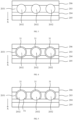
- FIG. 12 is a schematic diagram of an entire structure of a solar cell
- Fig. 13 is a schematic diagram illustrating a cross-sectional structural of a solar cell
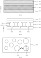
- Fig. 14 is a top view of a perovskite absorption layer 103.
- An X direction is a first direction.
- the solar cell includes: a first conductive layer 101, a first carrier transport layer 102, a perovskite absorption layer 103, and a second conductive layer 104 sequentially stacked in a first direction.
- the perovskite absorption layer 103 includes a bonding matrix 1031 and a plurality of monocrystal perovskite particles 1032 arranged in the bonding matrix 1031.
- the bonding matrix 1031 includes a first surface and a second surface that are opposite to each other, and the first surface faces the first conductive layer 101.
- At least some of the monocrystal perovskite particles 1032 have first convex surfaces and second convex surfaces, the first convex surfaces protrude relative to the first surface, and the second convex surfaces protrude relative to the second surface.
- a functional layer 30 is formed on a surface of the monocrystal perovskite particles 1032.
- the bonding matrix 1031 is configured to accommodate and fix the monocrystal perovskite particles 1032 arranged in the bonding matrix 1031. Therefore, transparent curable glue or colloid may be selected for construction, for example, ultraviolet curing glue or another type of curable transparent glue such as acrylic glue or resin glue is selected for constructing the bonding matrix 1031.
- Transparent means good light transmittance for visible light, for example, 80% or more transmittance for light of 400 nm or more, or 75% or more transmittance for light of 450 nm or more.
- the solar cell In the solar cell, light irradiated to the solar cell is absorbed through the perovskite absorption layer 103, then a photo-generated carrier is generated through the monocrystal perovskite particle 1032, different photo-generated carriers are collected through the first carrier transport layer 102 and the second conductive layer 104 respectively, and finally electric energy generated by the solar cell is transmitted to an external component through the first conductive layer 101 and the second conductive layer 104.
- the perovskite absorption layer 103 is constructed by using the bonding matrix 1031 and the plurality of monocrystal perovskite particles 1032 arranged in the bonding matrix 1031, so as to ensure integrity of the monocrystal perovskite particle 1032, avoid damage to a monocrystal perovskite material in the construction process of the perovskite absorption layer 103, and ensure that the photo-generated carrier generation capability of the perovskite absorption layer 103 is as good as possible.
- the perovskite absorption layer 103 is constructed by using the monocrystal perovskite particles 1032, so as to reduce a decomposition speed of the perovskite absorption layer 103 in the working process of the cell and ensure stability of the perovskite absorption layer 103 and the solar cell.
- the monocrystal perovskite particle 1032 has a longer carrier life, a higher carrier mobility, and a larger degree of diffusion. Therefore, the solar cell has higher photoelectric conversion efficiency and a longer service life.
- the perovskite absorption layer 103 is constructed by arranging the monocrystal perovskite particles 1032 in the bonding matrix 1031, so as to facilitate simple and efficient preparation of the large-area perovskite absorption layer 103, and break through the restriction of raw material generation efficiency of monocrystal perovskite on areas of the perovskite absorption layer 103 and the perovskite solar cell, so that preparation efficiency of the large-area solar cell with good stability is greatly improved, and an application prospect of the monocrystal perovskite solar cell is improved.
- the functional layer 30 is formed on the surface of the monocrystal perovskite particle 1032, and a function of the functional layer 30 is to compensate for the defect of the monocrystal perovskite particle 1032 and/or suppress decomposition of the monocrystal perovskite particle 1032. Therefore, the functional layer 30 is set to further reduce a decomposition probability of the monocrystal perovskite particle 1032 in the working process, thereby improving stability of the perovskite absorption layer 103 and the solar cell.
- the bonding matrix 1031 in the first direction, includes the first surface and the second surface that are opposite to each other. At least some of the monocrystal perovskite particles 1032 have the first convex surfaces and the second convex surfaces, the first convex surfaces protrude relative to the first surface, and the second convex surfaces protrude relative to the second surface.
- the perovskite absorption layer 103 In the process of constructing the perovskite absorption layer 103, it is ensured that at least some of the monocrystal perovskite particles 1032 have the first convex surfaces and the second convex surfaces that protrude relative to the two opposite surfaces of the bonding matrix 1031 respectively, that is, the at least some of the monocrystal perovskite particles 1032 pass through the bonding matrix 1031 and are in contact with the first carrier transport layer 102 and the second conductive layer 104.
- the at least some of the monocrystal perovskite particles 1032 have the first convex surfaces and the second convex surfaces, two opposite surfaces of the perovskite absorption layer 103 are texturing surfaces, thereby improving a light absorption capability of the perovskite absorption layer 103.
- the at least some of the monocrystal perovskite particles 1032 pass through the bonding matrix 1031 and are in contact with the first carrier transport layer 102 and the second conductive layer 104, after photo-generated carriers are generated, the difficulty in moving the photo-generated carriers to the first carrier transport layer 102 and the second conductive layer 104 is greatly reduced, and a photo-generated carrier transport capability of the perovskite absorption layer 103 is improved. Further, photoelectric conversion efficiency of the perovskite absorption layer 103 is improved in terms of the light absorption capability and the carrier transport capability.
- the monocrystal perovskite particle 1032 may be in a shape of a regular polyhedron including a sphere, a near sphere, and a cube, an irregular polyhedron or the like. Sizes and shapes of the monocrystal perovskite particles 1032 included in the perovskite absorption layer 103 may be consistent or may be inconsistent. This is not limited in this embodiment of the present disclosure. In this embodiment of the present disclosure, for ease of understanding and description, an example in which the perovskite particle is in the shape of sphere is used for description, and the shape of the monocrystal perovskite particle 1032 may be adjusted as required in an actual use process. This is not limited in this embodiment of the present disclosure.
- a respective monocrystal perovskite particle 1032 included in the perovskite absorption layer 103 may have the first convex surface and the second convex surface.
- at least some particles may have the first convex surface and the second convex surface, and the remaining particles may include one or more particles that have only the first convex surface, or have only the second convex surface, or have neither the first convex surface nor the second convex surface.
- the functional layer 30 may be formed on the surface of a respective monocrystal perovskite particle 1032, or the functional layers 30 may be formed on the surfaces of some of the monocrystal perovskite particles 1032. This is not limited in this embodiment of the present disclosure.
- the monocrystal perovskite particles 1032 in the perovskite absorption layer 103 may be arranged into an ordered array in the bonding matrix 1031 according to a fixed interval, for example, arranged into a regular array in a shape of a rectangle, a near rectangle, a circle, an oval, or the like, to further improve uniformity of light absorption and carrier output by the perovskite absorption layer 103.
- the monocrystal perovskite particles 1032 may be freely arranged in the bonding matrix 1031 according to an unfixed interval and order.
- the functional layer 30 includes a first functional layer 31 covering the entire surface of the monocrystal perovskite particle 1032.
- the first functional layer 31 covering the entire surface of the monocrystal perovskite particle 1032 is formed on the surface of the monocrystal perovskite particle 1032. Then the perovskite absorption layer 103 is formed by using the monocrystal perovskite particle 1032 of which the entire surface is covered by the first functional layer 31, and the first functional layer 31 is used as the functional layer 30 on the surface of a respective monocrystal perovskite particle 1032 in the perovskite absorption layer 103.
- the first functional layer 31 covering the entire surface is formed on the surface of the monocrystal perovskite particle 1032, to ensure that any of the monocrystal perovskite particles 1032 has relatively good stability in the working process, thereby ensuring the stability of the solar cell.
- the functional layer 30 includes a second functional layer 32 covering the remaining surface of the monocrystal perovskite particle 1032 other than the first convex surface T1.
- Fig. 16 is a cross-sectional view of a solar cell passing through a spherical center of the monocrystal perovskite particle 1032.
- a functional film layer covering the entire surface of the monocrystal perovskite particle 1032 may be first formed on the surface of the monocrystal perovskite particle 1032, then the functional film layer on the first convex surface T1 of the monocrystal perovskite particle 1032 is removed, to obtain the second functional layer 32 covering the remaining surface of the monocrystal perovskite particle 1032 other than the first convex surface T1, and the second functional layer 32 is used as the functional layer 30 on the surface of the monocrystal perovskite particle 1032.
- the second functional layer 32 covering the remaining surface of the monocrystal perovskite particle 1032 other than the first convex surface T1 is formed as the functional layer 30 on the surface of the monocrystal perovskite particle 1032, so that the stability of the monocrystal perovskite particle 1032 in the working process is ensured as much as possible, and light reflectivity of the first convex surface T1 is reduced, thereby ensuring that the monocrystal perovskite particle 1032 has a good light absorption capability, and further ensuring a carrier generation capability of the monocrystal perovskite particle 1032 and the photoelectric conversion capability of the solar cell.
- the second functional layer 32 does not completely cover the first convex surface T1 is used for description.
- the second functional layer 32 may not completely cover the first convex surface T1, or the second functional layer 32 may cover only a part of the first convex surface T1.
- a specific arrangement manner may be adjusted according to a requirement for the stability and/or the light absorption capability of the monocrystal perovskite particle 1032. This is not limited in this embodiment of the present disclosure.
- the functional layer 30 includes a third functional layer 33 covering the remaining surface of the monocrystal perovskite particle 1032 other than the second convex surface T2.
- Fig. 17 is a cross-sectional view of a solar cell passing through a spherical center of the monocrystal perovskite particle 1032.
- a functional film layer covering the entire surface of the monocrystal perovskite particle 1032 may be first formed on the surface of the monocrystal perovskite particle 1032, then the functional film layer on the second convex surface T2 of the monocrystal perovskite particle 1032 is removed, to obtain the third functional layer 33 covering the remaining surface of the monocrystal perovskite particle 1032 other than the second convex surface T2, and the third functional layer 33 is used as the functional layer 30 on the surface of the monocrystal perovskite particle 1032.
- the third functional layer 33 covering the remaining surface of the monocrystal perovskite particle 1032 other than the second convex surface T2 is formed as the functional layer 30 on the surface of the monocrystal perovskite particle 1032, so that the stability of the monocrystal perovskite particle 1032 in the working process is ensured as much as possible, and light reflectivity of the second convex surface T2 is reduced, thereby ensuring that the monocrystal perovskite particle 1032 has a good light absorption capability, and further ensuring a carrier generation capability of the monocrystal perovskite particle 1032 and the photoelectric conversion capability of the solar cell.
- the third functional layer 33 does not completely cover the second convex surface T2 is used for description.
- the third functional layer 33 may not completely cover the second convex surface T2, or the third functional layer 33 may cover only a part of the second convex surface T2.
- a specific arrangement manner may be adjusted according to a requirement for the stability and/or the light absorption capability of the monocrystal perovskite particle 1032. This is not limited in this embodiment of the present disclosure.
- the functional layer 30 include a fourth functional layers 34 covering the remaining surface of the monocrystal perovskite particle 1032 other than the first convex surface T1 and the second convex surface T2.
- Fig. 18 is a cross-sectional view of a solar cell passing through a spherical center of the monocrystal perovskite particle 1032.
- a functional film layer covering the entire surface of the monocrystal perovskite particle 1032 may be first formed on the surface of the monocrystal perovskite particle 1032, then the functional film layer on the second convex surface T2 of the monocrystal perovskite particle 1032 is removed, to obtain the fourth functional layer 34 covering the remaining surface of the monocrystal perovskite particle 1032 other than the second convex surface T2, and the fourth functional layer 34 is used as the functional layer 30 on the surface of the monocrystal perovskite particle 1032.
- the fourth functional layer 34 covering the remaining surface of the monocrystal perovskite particle 1032 other than the first convex surface T1 and the second convex surface T2 is formed as the functional layer 30 on the surface of the monocrystal perovskite particle 1032, so that the stability of the monocrystal perovskite particle 1032 in the working process is ensured to some extent, and light reflectivity of the first convex surface T1 and the second convex surface T2 is reduced, thereby ensuring that the monocrystal perovskite particle 1032 has a good light absorption capability, and further ensuring a carrier generation capability of the monocrystal perovskite particle 1032 and the photoelectric conversion capability of the solar cell.
- the functional layer 30 include a fifth functional layer 35 covering the first convex surface T1 and the first surface.
- Fig. 19 is a cross-sectional view of a solar cell passing through a spherical center of the monocrystal perovskite particle 1032.
- the fifth functional layer 35 is directly formed on a surface of the perovskite absorption layer 103 facing the first conductive layer 101, the fifth functional layer 35 covers the first surface of the bonding matrix 1031 and the first convex surface T1 of the monocrystal perovskite particle 1032, and the fifth functional layer 35 on the first convex surface T1 of the monocrystal perovskite particle 1032 is used as the functional layer 30 on the surface of the monocrystal perovskite particle 1032.
- the fifth functional layer 35 covering the first surface of the bonding matrix 1031 and the first convex surface T1 of the monocrystal perovskite particle 1032 is used as the functional layer 30, so that the surface of the first convex surface T1 of the monocrystal perovskite particle 1032 has the functional layer 30, to improve the stability of the monocrystal perovskite particle 1032 in the working process.
- the fifth functional layer 35 covers the first surface of the bonding matrix 1031, so that reflectivity of light inside the bonding matrix 1031 is increased, and the light absorption capability of the perovskite absorption layer 103 is enhanced, thereby improving the photoelectric conversion capability of the solar cell.
- the fifth functional layer 35 may be integrally formed on the surface of the perovskite absorption layer 103 directly and covers the first convex surface T1 of a respective monocrystal perovskite particle 1032, or may be selectively formed on the surface of the perovskite absorption layer 103 according to a specific pattern and does not cover all regions on the first convex surfaces T1 of all the monocrystal perovskite particles 1032 and the first surface of the bonding matrix 1031.
- the fifth functional layer 35 may cover the entire first convex surface T1 or may cover only a part of the first convex surface T1. This is not limited in this embodiment of the present disclosure.
- the functional layer 30 includes a sixth functional layer 36 covering the second convex surface T2 and the second surface.
- Fig. 20 is a cross-sectional view of a solar cell passing through a spherical center of the monocrystal perovskite particle 1032.
- the sixth functional layer 36 is directly formed on a second surface of the perovskite absorption layer 103 opposite to a first surface facing the first conductive layer 101 in the first direction, the sixth functional layer 36 covers the second surface of the bonding matrix 1031 and the second convex surface T2 of the monocrystal perovskite particle 1032, and the sixth functional layer 36 on the second convex surface T2 of the monocrystal perovskite particle 1032 is used as the functional layer 30 on the surface of the monocrystal perovskite particle 1032.
- the sixth functional layer 36 covering the second surface of the bonding matrix 1031 and the second convex surface T2 of the monocrystal perovskite particle 1032 is used as the functional layer 30, so that the surface of the second convex surface T2 of the monocrystal perovskite particle 1032 has the functional layer 30, to improve the stability of the monocrystal perovskite particle 1032 in the working process.
- the sixth functional layer 36 covers the second surface of the bonding matrix 1031, so that reflectivity of light inside the bonding matrix 1031 is increased, and the light absorption capability of the perovskite absorption layer 103 is enhanced, thereby improving the photoelectric conversion capability of the solar cell.
- the sixth functional layer 36 may be integrally formed on the surface of the perovskite absorption layer 103 directly and covers the second convex surface T2 of each monocrystal perovskite particle 1032, or may be selectively formed on the surface of the perovskite absorption layer 103 according to a specific pattern and does not cover all regions on the second convex surfaces T2 of all the monocrystal perovskite particles 1032 and the second surface of the bonding matrix 1031.
- the sixth functional layer 36 may cover the entire second convex surface T2 or may cover only a part of the second convex surface T2. This is not limited in this embodiment of the present disclosure.
- one of the two figures in Fig. 21 is a cross-sectional view of a solar cell in which the functional layer 30 is formed by the fourth functional layer 34 only covering the remaining surface of the monocrystal perovskite particle other than the first convex surface T1 and the second convex surface T2, the fifth functional layer 35 covering the first convex surface T1 and the first surface of the bonding matrix 1031, and the sixth functional layer 36 covering the second convex surface T2 and the second surface of the bonding matrix 1031, and the other of the two figures in is a cross-sectional view of a solar cell in which the functional layer 30 is formed by the second functional layer 32 covering the remaining surface of the monocrystal perovskite particle other than the first convex surface T1 and the sixth functional layer 36 covering the second convex surface T2 and the second surface of
- the functional layer 30 may be formed by only any one of the first functional layer 31 to the sixth functional layer 36, the first functional layer 31 and the fifth functional layer 35 and/or the sixth functional layer 36, the second functional layer 32 and the fifth functional layer 35 and/or the sixth functional layer 36, the third functional layer 33 and the fifth functional layer 35 and/or the sixth functional layer 36, the fourth functional layer 34 and the fifth functional layer 35 and/or the sixth functional layer 36, or the fifth functional layer 35 and the sixth functional layer 36.
- a cross-sectional view of a solar cell in which the functional layer 30 is formed in a remaining construction manner is not shown one by one again.
- a selected construction material may be further adjusted according to a specific type of a carrier transport layer with a largest contact area.
- the carrier transport layer includes an electron transport layer and a hole transport layer.
- lithium fluoride (LiF) or magnesium fluoride (MgF 2 ) or the like may be selected as the construction material.
- poly[(9,9-bis(3'-(N,N-dimethylamino)propyl fluorenyl-2,7-fluorene)-alt-[(9,9-dioctylfluorene 2,7-fluorene)-dibromine (PFN-Br) or poly[bis(4-phenyl)(4-butylphenyl)amine] (TPD) may be selected as the construction material.
- trimercapto-s-triazine trisodium salt may be selected as the construction material.
- a proper material is selectively selected according to contact areas of different carrier transport layers to construct the functional layer 30, to improve construction accuracy and a usage effect of the functional layer 30.
- a specific construction manner is not limited in this embodiment of the present disclosure.
- the functional layer 30 has a thickness in a range of 0.1 nm to 1 ⁇ m.
- the thickness of the functional layer 30 is associated with the composition of the functional layer 30.
- the thickness of the functional layer 30 may be represented by an average distance or a maximum distance between two opposite points on the fifth functional layer 35 and/or the sixth functional layer 36 in the first direction.
- the thickness of the functional layer 30 may be represented by an average distance or a maximum distance between any point on a surface of the first functional layer 31, second functional layer 32, third functional layer 33, or fourth functional layer 34 away from the monocrystal perovskite particle 1032 and a surface of the monocrystal perovskite particle close to the functional layer 30.
- the thickness of the functional layer 30 When the thickness of the functional layer 30 is excessively large, the stability of the monocrystal perovskite particle 1032 can be effectively improved, but the light absorption capability of the monocrystal perovskite particle 1032 is reduced, and the photoelectric conversion capability of the solar cell is reduced.
- the thickness of the functional layer 30 is excessively large, the light absorption capability of the monocrystal perovskite particle 1032 is ensured, but the decomposition probability is large, the stability of the solar cell cannot be ensured, and the improvement of the light absorption capability of the solar cell is relatively limited.
- the thickness of the functional layer 30 is set in a range of 0.1 nm to 1 ⁇ m, for example, set to 0.1 nm, 0.5 nm, 1 nm, 5 nm, 10 nm, 25 nm, 50 nm, 100 nm, 200 nm, 500 nm, 750 nm, or 900 nm.
- the thickness of the functional layer 30 is ensured that the monocrystal perovskite particle 1032 and the solar cell have good light absorption capabilities, and the photoelectric conversion capability of the solar cell is ensured while the stability of the solar is improved as much as possible.
- a distance between the respective monocrystal perovskite particle and an adjacent monocrystal perovskite particle 1032 is not greater than a maximum distance between any two points on a surface of the respective monocrystal perovskite particle 1032.
- two largest circles in the figure are circles formed in a horizontal direction through spherical centers of two adjacent monocrystal perovskite particles 1032.
- a maximum distance between any two points on a surface of a current monocrystal perovskite particle is marked as d
- a distance between the monocrystaltwo adjacent monocrystal perovskite particles 1032 is marked as D.
- D may represent a minimum value of the distance between any point on the surface of one of the two adjacent monocrystal perovskite particles and any point on the surface of the other of the two adjacent monocrystal perovskite particles 1032.
- the distance D between two adjacent monocrystal perovskite particles 1032 in the perovskite absorption layer 103 needs to be limited, and the distance D between the respective monocrystal perovskite particle and the adjacent monocrystal perovskite particle 1032 is set in a range less than a size of the respective perovskite particle, that is, set in a range less than the maximum distance d between any two points on the surface of the respective monocrystal perovskite particle, for example, set D to be equal to 0.1d, 0.2d, 0.35d, 0.45d, 0.5d, 0.75d, or 0.9d.
- the distance between the respective monocrystal perovskite particle and the adjacent monocrystal perovskite particle 1032 is set in a range not greater than the size of the respective monocrystal perovskite particle, so that the perovskite absorption layer 103 has a good light absorption capability, thereby avoiding a problem that the photoelectric conversion efficiency of the solar cell decreases due to the decrease of the light absorption capability.
- a distance between any point on the first convex surface and the first surface and/or a distance between any point on the second convex surface and the second surface is not greater than half of a maximum length of the monocrystal perovskite particle 1032 in the first direction.
- Fig. 22 is a cross-sectional view of the perovskite absorption layer 103 formed through spherical centers of three monocrystal perovskite particles 1032 having a same size in a vertical direction.
- a maximum distance between any point on the first convex surface of the monocrystal perovskite particle 1032 and the first surface of the bonding matrix 1031 is a distance a between a point A on the first convex surface farthest from the first surface and the first surface.
- a maximum distance between any point on the second convex surface of the monocrystal perovskite particle 1032 and the second surface of the bonding matrix 1031 is a distance b between a point B on the second convex surface farthest from the second surface and the first surface.
- a maximum length of the monocrystal perovskite particle 1032 is L.
- the function of the bonding matrix 1031 is to fix the monocrystal perovskite particles 1032, and the bonding matrix 1031 has a specific thickness to ensure a fixing effect.
- the monocrystal perovskite particle 1032 generates a carrier, different carriers are aggregated and move toward two ends of the monocrystal perovskite particle 1032 respectively.
- the carriers aggregated on the first carrier transport layer 102 or the second conductive layer 104 may be recombined with carriers of opposite polarity, resulting in reduction in the photoelectric conversion efficiency of the perovskite absorption layer 103.
- the distance between any point on the first convex surface of the monocrystal perovskite particle 1032 and the first surface and/or the distance between any point on the second convex surface and the second surface is not greater than half of a maximum length of the monocrystal perovskite particle 1032 in the first direction.
- the distance a and/or the distance b is set to 0.1L, 0.15L, 0.2L, 0.25L, 0.35L, 0.45L, or 0.49L.
- the distance between any point on the first convex surface of the monocrystal perovskite particle 1032 and the first surface and/or the distance between any point on the second convex surface and the second surface is limited, to reduce a recombination probability of carriers of opposite polarities as much as possible and ensure the photoelectric conversion efficiency of the solar cell.
- a maximum distance between any two points on a surface of the monocrystal perovskite particle 1032 is in a range of 5 ⁇ m to 100 ⁇ m.
- the perovskite absorption layer 103 In the process of constructing the perovskite absorption layer 103, if a size of a selected monocrystal perovskite particle 1032 is excessively large, that is, when a maximum distance d between any two points on a surface of the particle is excessively large, after a perovskite absorption layer is constructed by using the monocrystal perovskite particle 1032, after carriers are generated by absorbing light energy, a distance that the carriers needs to move in a process of migrating to the first carrier transport layer 102 or the second conductive layer 104 is excessively large. Consequently, it is difficult to complete carrier migration, and the photoelectric conversion efficiency of the solar cell is further reduced.
- the size of the monocrystal perovskite particle 1032 is excessively small, that is, when the maximum distance d between any two points on the surface of the particle is excessively small, in a carrier migration process, a distance between different carriers is small. Therefore, recombination of the carriers is easy to occur, resulting in reduction in the photoelectric conversion efficiency of the solar cell.
- the thickness of the perovskite absorption layer 103 is also small, a decomposition probability of the monocrystal perovskite particle 1032 is greatly increased under an action of a potential difference between two sides, resulting in reduction of the stability of the solar cell.
- a monocrystal perovskite particle 1032 with a maximum distance in a range of 5 ⁇ m to 100 ⁇ m between any two points on a surface of the particle is selected for construction.
- a monocrystal perovskite particle 1032 with a maximum distance of 5 ⁇ m, 7.5 ⁇ m, 10 ⁇ m, 15 ⁇ m, 25 ⁇ m, 60 ⁇ m, 80 ⁇ m, 85 ⁇ m, or 95 ⁇ m between any two points on a surface of the particle is selected for constructing the perovskite absorption layer 103.
- the carriers in the perovskite absorption layer 103 can be easily migrated, and a recombination probability between different carriers and the decomposition probability of the monocrystal perovskite particle 1032 are reduced, thereby ensuring the photoelectric conversion efficiency and stability of the solar cell.
- an area of an orthographic projection of the perovskite absorption layer 103 on the first conductive layer 101 is a first area
- an area of an orthographic projection of the plurality of monocrystal perovskite particles 1032 on the first conductive layer 101 is a second area
- a ratio of the second area to the first area is in a range of 0.3 to 0.9.
- a light absorption area when the perovskite absorption layer 103 performs photoelectric conversion may be considered as a sum of orthographic projection areas of all the monocrystal perovskite particles 1032 on the first conductive layer 101, that is, the second area.
- An area for the perovskite absorption layer 103 to receive light may be considered as an orthographic projection area of the perovskite absorption layer 103 on the first conductive layer 101, that is, the first area.
- the perovskite absorption layer 103 When the ratio of the second area to the first area is excessively small, the perovskite absorption layer 103 has low absorption utilization on light irradiated on the perovskite absorption layer 103, which results in a weak photoelectric conversion capability of the solar cell and is difficult to effectively perform photoelectric conversion. Due to the limitation of the photoelectric conversion capability of the monocrystal perovskite particle 1032, the perovskite absorption layer 103 has an upper limit on absorption utilization on light irradiated on the perovskite absorption layer 103.
- the perovskite absorption layer 103 has the monocrystal perovskite particle 1032 of which the photoelectric conversion capability is not fully used, and a cost/performance ratio between the manufacturing cost of the solar cell and the photoelectric conversion capability is relatively low.
- a ratio of an area of an orthographic projection of the monocrystal perovskite particles 1032 in the perovskite absorption layer 103 on the first conductive layer 101 to the area of the orthographic projection of the perovskite absorption layer 103 on the first conductive layer 101 needs to be limited.
- the ratio of the second area to the first area is controlled to be within a range of 0.3 to 0.9, for example, 0.3, 0.35, 0.45, 0.5, 0.65, 0.7, 0.75. 0.8, or 0.85.
- a sum of the areas of the orthographic projections of the monocrystal perovskite particles 1032 on the first conductive layer 101 and the area of the orthographic projection of the perovskite absorption layer 103 on the first conductive layer 101 are limited in a specific range, to ensure the absorption utilization of the perovskite absorption layer 103 on the light and reduce the preparation costs of the solar cell as much as possible.
- the perovskite absorption layer 103 in the process of constructing the perovskite absorption layer 103, reference may be made to a light transmission requirement on a top cell when a tandem solar cell is constructed by using the perovskite cell as the top cell.
- a ratio of an illumination area required by the bottom cell to an area of a light receiving surface of the bottom cell is determined when the tandem solar cell has the optimal or good photoelectric conversion efficiency.
- the ratio of the second area to the first area in the perovskite absorption layer 103 is set according to the determined ratio.
- the tandem solar cell has the optimal photoelectric conversion efficiency, and thus the ratio of the second area to the first area in the perovskite absorption layer 103 may be correspondingly set to 0.7, 0.5, and 0.3 respectively.
- the monocrystal perovskite particle 1032 with a bandgap in a range of 1 eV to 2 eV may be selected to construct the perovskite solar cell.
- the photoelectric conversion efficiency of the tandem solar cell is further related to the bandgap of the monocrystal perovskite particles 1032 in the top cell.
- the monocrystal perovskite particles 1032 with a bandgap in a range of 1.4 eV to 1.8 eV may be selected according to the type of the bottom cell to construct the perovskite cell.
- a specific bandgap of the selected monocrystal perovskite particle 1032 is not limited in this embodiment of the present disclosure.
- the ratio of the second area to the first area in the perovskite absorption layer 103 in the perovskite solar cell and the bandgap of the monocrystal perovskite particle 1032 can be respectively controlled according to a requirement in which the tandem solar cell achieves good photoelectric conversion efficiency to improve the photoelectric conversion efficiency of the tandem solar cell as much as possible.
- the plurality of monocrystal perovskite particles 1032 may include perovskite particles having no first convex surface and/or second convex surface, and photo-generated carriers generated in the monocrystal perovskite particles 1032 including neither the first convex surface nor the second convex surface are difficult to complete carrier migration due to the limitation of the bonding matrix 1031.
- the second area when the second area is calculated, only a sum of areas of orthographic projections of the monocrystal perovskite particles 1032 including the first convex surface and the second convex surface on the first conductive layer 101 may be calculated.
- orthographic projections of all the monocrystal perovskite particles 1032 having the first convex surfaces and/or the second convex surface on the first conductive layer 101 may be counted. This is not limited in this embodiment of the present disclosure.
- the bonding matrix 1031 has a thickness not less than 100 nm.
- the thickness h of the bonding matrix 1031 may be represented by using a distance between two opposite points on the first surface and the second surface of the bonding matrix 1031 in the first direction.
- An important function of the bonding matrix 1031 is to fix the monocrystal perovskite particles 1032 arranged in the bonding matrix 1031. Therefore, when the thickness h of the bonding matrix 1031 in the first direction is excessively small, it is difficult to stably fix the monocrystal perovskite particles 1032, and a problem such as a crack may occur, resulting in reduction in the stability of the solar cell.
- a distance between different carriers may be excessively small, resulting in recombination of different carriers, and further resulting in reduction in the photoelectric conversion efficiency of the solar cell.
- the thickness h of the bonding matrix 1031 in the first direction is not less than 100 nm, for example, 100 nm, 200 nm, 350 nm, 500 nm, 800 nm, 1 ⁇ m, 5 ⁇ m, 20 ⁇ m, or 50 ⁇ m.
- the thickness of the bonding matrix 1031 in the first direction is set sufficiently large to ensure that the bonding matrix 1031 can stably fix the monocrystal perovskite particles 1032, avoid failure of the perovskite absorption layer 103, and improve the stability of the solar cell.
- it is ensured that the distance between different carriers is sufficiently large to avoid recombination of different carriers, and ensure the photoelectric conversion efficiency of the solar cell.
- the size of the monocrystal perovskite particle 1032 is also increased, which increases the difficulty in migrating the photo-generated carriers generated by the monocrystal perovskite particle 1032, and further causes reduction in the photoelectric conversion efficiency of the solar cell.
- the thickness h of the bonding matrix 1031 in the first direction is set to a range less than a size of the monocrystal perovskite particle 1032 with good photoelectric conversion efficiency, to ensure that the perovskite absorption layer 103 has good photoelectric conversion efficiency as much as possible.
- the bonding matrix 1031 includes a light trapping surface 1033 facing the first carrier transport layer 102 and/or facing the second conductive layer 104.
- Fig. 23 to Fig. 25 are all cross-sectional views of a solar cell in a vertical direction.
- the light trapping surface 1033 includes only a surface of the bonding matrix 1031 facing the first carrier transport layer 102.
- the light trapping surface 1033 includes only a surface of the bonding matrix 1031 facing the second conductive layer 104.
- the light trapping surface 1033 includes the surface of the bonding matrix 1031 facing the first carrier transport layer 102 and the surface facing the second conductive layer 104.
- Another important function of the bonding matrix 1031 is to ensure a light absorption capability of the perovskite absorption layer 103.
- the light trapping surface 1033 that improves the light absorption capability of the perovskite absorption layer 103 may be further manufactured on the bonding matrix 1031.
- the light trapping surface 1033 may include only the surface of the bonding matrix 1031 facing the first carrier transport layer 102, or include only the surface of the bonding matrix 1031 facing the second conductive layer 104, or include both the surface of the bonding matrix 1031 facing the first carrier transport layer 102 and the surface facing the second conductive layer 104.
- the light trapping surface 1033 facing the first carrier transport layer 102 and/or the second conductive layer 104 is formed on the bonding matrix 1031, so that a light path of light irradiated on the perovskite absorption layer 103 in the perovskite absorption layer 103 is increased, to improve the light absorption capability of the perovskite absorption layer 103, thereby improving the photoelectric conversion efficiency of the perovskite absorption layer 103 and the solar cell.
- the light trapping surface 1033 includes a first light trapping structure 311, and in the first direction, the first light trapping structure 311 extends to the outside of the bonding matrix 1031.
- Fig. 26 is a cross-sectional view of a solar cell in which the light trapping surface 1033 includes both the surface of the bonding matrix 1031 facing the first carrier transport layer and the surface facing the second conductive layer 104 and the light trapping surface 1033 includes the first light trapping structure 311.
- the first light trapping structure 311 may be formed on the surface of the bonding matrix 1031 facing the first carrier transport layer 102 and/or facing the second conductive layer 104, that is, one or more protrusions extending in a direction away from the bonding matrix 1031 are formed on the first surface or the second surface.
- the first light trapping structure 311 is located on the first surface and/or the second surface, a position relationship between any surface of the first light trapping structure 311 and the first convex surface and/or the second convex surface of each monocrystal perovskite particle 1032 in the perovskite absorption layer 103 is tangent or separated, and the first light trapping structure 311 does not affect a contact area between the first convex surface and the first carrier transport layer 102 and a contact area between the second convex surface and the second conductive layer 104.
- One or more protrusions extending in the direction away from the bonding matrix 1031 are formed on the first surface and/or the second surface as the first light trapping structures 311, so that the first surface and/or the second surface is changed into the light trapping surface 1033 that has a capability of extending a light path of incident light in the perovskite absorption layer 103, to improve an absorption and utilization capability of the perovskite absorption layer 103 on the incident light, thereby improving the photoelectric conversion capability and efficiency of the perovskite absorption layer 103.
- shapes and a sizes of the first light trapping structures 311 may be the same or may be different. This is not limited in this embodiment of the present disclosure.
- the light trapping surface 1033 includes a second light trapping structure 312, and in the first direction, the second light trapping structure 312 is recessed to the inside of the bonding matrix 1031.
- Fig. 27 is a cross-sectional view of a solar cell in which the light trapping surface 1033 includes both the surface of the bonding matrix 1031 facing the first carrier transport layer and the surface facing the second conductive layer 104 and the light trapping surface 1033 includes the second light trapping structure 312.
- the second light trapping structure 312 may be formed on the surface of the bonding matrix 1031 facing the first carrier transport layer 102 and/or facing the second conductive layer 104, that is, one or more recesses extending to the inside of the bonding matrix 1031 are formed on the first surface or the second surface.
- the second light trapping structure 312 is located on the first surface and/or the second surface, a position relationship between any surface of the second light trapping structure 312 and a surface of each monocrystal perovskite particle 1032 in the perovskite absorption layer 103 located inside the bonding matrix 1031 is tangent or separated, and the second light trapping structure 312 does not affect a contact area between the monocrystal perovskite particle 1032 and the bonding matrix 1031.
- One or more recesses extending to the inside of the bonding matrix 1031 are formed on the first surface or the second surface as the second light trapping structures 312, so that the first surface and/or the second surface is changed into the light trapping surface 1033 that has a capability of extending a light path of incident light in the perovskite absorption layer 103, to improve an absorption and utilization capability of the perovskite absorption layer 103 on the incident light, thereby improving the photoelectric conversion capability and efficiency of the perovskite absorption layer 103.
- the light trapping surface 1033 may include only one or more first light trapping structures 311, or may include only one or more second light trapping structures 312, or may include one or more first light trapping structures 311 and one or more second light trapping structures 312.
- the light trapping surface 1033 may include only the surface of the bonding matrix 1031 facing the first carrier transport layer 102, or may include only the surface of the bonding matrix 1031 facing the second conductive layer 104, or may include both the surface of the bonding matrix 1031 facing the first carrier transport layer 102 and the surface of the bonding matrix 1031 facing the second conductive layer 104.
- Specific arrangement of the light trapping surface 1033 and a type and a quantity of light trapping structures included in the light trapping surface 1033 are not limited in this embodiment of the present disclosure.
- shapes and sizes of the second light trapping structures 312 may be the same or may be different. This is not limited in this embodiment of the present disclosure.
- the first carrier transport layer 102 is an electron transport layer or a hole transport layer.
- a function of the first carrier transport layer 102 is to collect and transmit carriers generated in the perovskite absorption layer 103.
- the first carrier transport layer 102 may be the hole transport layer or may be the electron transport layer.
- the function of the first carrier transport layer 102 includes aggregating electrons, transmitting the aggregated electrons to the first conductive layer 101 for the first conductive layer 101 to perform power output, and preventing holes from directly flowing to the first conductive layer 101.
- the function of the first carrier transport layer 102 includes preventing the electrons from entering the first conductive layer 101 and enhancing transport of the holes, to prevent the perovskite absorption layer 103 from being in direct contact with the first conductive layer 101.
- the photoelectric conversion capability and power output of the solar cell are ensured.
- the electron transport layer may be made of materials including tin oxide (SnOx), titanium dioxide (TiO 2 ), and fullerene and its derivation such as C 60 and PCBM.
- the hole transport layer may be made of a material such as poly[bis(4-phenyl)(2,4,6-trimethylbenzyl)amine] (PTAA), 2,2',7,7'-tetra[N,N-bis(4-methoxyphenyl)amino]-9,9'-spirobifluorene (spiro-OMeTAD), nickel oxide (NiOx), or cuprous rhodanide (CuSCN).
- PTAA poly[bis(4-phenyl)(2,4,6-trimethylbenzyl)amine]
- spiro-OMeTAD 2,2',7,7'-tetra[N,N-bis(4-methoxyphenyl)amino]-9,9'-spirobifluorene
- NiOx nickel
- the first carrier transport layer 102 in the first direction, has a thickness in a range of 1 nm to 1 ⁇ m.
- a core function of the first carrier transport layer 102 is to improve aggregation and transport capabilities for one type of carriers and also isolate contact between another type of carriers and the first conductive layer 101. Therefore, when the thickness of the first carrier transport layer 102 in the first direction is excessively large, a migration distance is excessively large when the carrier is transmitted to the first conductive layer 101, carrier recombination may occur, resulting in a relatively large carrier loss and reduction in the photoelectric conversion efficiency of the solar cell.
- the first carrier transport layer 102 When the thickness of the first carrier transport layer 102 in the first direction is excessively small, the first carrier transport layer 102 has limited aggregation and transport capabilities for the carriers, and cannot aggregate and transmit all carriers of a specific type generated by the perovskite absorption layer 103 in time, resulting in a relatively large carrier loss and affecting the photoelectric conversion efficiency of the solar cell. In addition, when the thickness is excessively small, an isolation capability for another type of carriers is also reduced, resulting in recombination of carriers of different types and further affecting the photoelectric conversion efficiency of the solar cell.
- the thickness of the first carrier transport layer 102 in the first direction is set to between 1 nm and 1 ⁇ m, for example, set to 1 nm, 5 nm, 10 nm, 50 nm, 100 nm, 200 nm, 250 nm, 400 nm, 500 nm, 650 nm, 750 nm, 800 nm, or 950 nm. It is ensured that the first carrier transport layer 102 has sufficiently large aggregation and transport capabilities for a type of carriers, and has a sufficiently large isolation capability for another type of carriers, so as to reduce the carrier loss caused by carrier recombination and migration, and ensure the photoelectric conversion efficiency of the solar cell.
- the solar cell further includes: a second carrier transport layer 105, where the second carrier transport layer 105 is located between the perovskite absorption layer 103 and the second conductive layer 104 and is in contact with the perovskite absorption layer 103 and the second conductive layer 104 respectively.
- a function of the second carrier transport layer 105 is similar to that of the first carrier transport layer 102 and is to collect and transmit carriers generated in the perovskite absorption layer 103.
- the second carrier transport layer 105 may be a hole transport layer or may be an electron transport layer.
- the function of the second carrier transport layer 105 includes aggregating electrons, transmitting the aggregated electrons to the first conductive layer 101 for the first conductive layer 101 to perform power output, and preventing holes from directly flowing to the first conductive layer 101.
- the function of the second carrier transport layer 105 includes preventing the electrons from entering the first conductive layer 101 and enhancing transport of the holes, to prevent the perovskite absorption layer 103 from being in direct contact with the first conductive layer 101.
- the photoelectric conversion capability and power output of the solar cell are ensured.
- the second carrier transport layer 105 in the first direction, has a thickness in a range of 1 nm to 1 ⁇ m.
- a core function of the second carrier transport layer 105 is to improve aggregation and transport capabilities for one type of carriers and also isolate contact between another type of carriers and the first conductive layer 101. Therefore, when the thickness of the second carrier transport layer 105 in the first direction is excessively large, a migration distance is excessively large when the carriers are transmitted to the second conductive layer 104, carrier recombination may occur, resulting in a relatively large carrier loss and reduction in the photoelectric conversion efficiency of the solar cell.
- the second carrier transport layer 105 When the thickness of the second carrier transport layer 105 in the first direction is excessively small, the second carrier transport layer 105 has limited aggregation and transport capabilities for the carriers, and cannot aggregate and transmit all carriers of a specific type generated by the perovskite absorption layer 103 in time, resulting in a relatively large carrier loss and affecting the photoelectric conversion efficiency of the solar cell. In addition, when the thickness is excessively small, an isolation capability for another type of carriers is also reduced, resulting in recombination of carriers of different types and further affecting the photoelectric conversion efficiency of the solar cell.
- the thickness of the second carrier transport layer 105 in the first direction is set to between 1 nm and 1 ⁇ m, for example, set to 1 nm, 5 nm, 10 nm, 50 nm, 100 nm, 200 nm, 250 nm, 400 nm, 500 nm, 650 nm, 750 nm, 800 nm, or 950 nm. It is ensured that the second carrier transport layer 105 has sufficiently large aggregation and transport capabilities for one type of carriers, and has a sufficiently large isolation capability for another type of carriers, so as to reduce the carrier loss caused by carrier recombination and migration, and ensure the photoelectric conversion efficiency of the solar cell.
- the second carrier transport layer 105 when the first carrier transport layer 102 is the hole transport layer, the second carrier transport layer 105 is the electron transport layer; and when the first carrier transport layer 102 is the electron transport layer, the second carrier transport layer 105 is the hole transport layer.
- carrier transport layers for aggregating and transmitting different carriers may be arranged on two opposite sides of the perovskite absorption layer 103 in the first direction respectively, to improve the photoelectric conversion efficiency and stability of the solar cell as much as possible.
- the perovskite absorption layer 103 of the solar cell is formed by the bonding matrix 1031 and the plurality of monocrystal perovskite particles 1032 arranged in the bonding matrix 1031.
- the perovskite absorption layer 103 is constructed by using the monocrystal perovskite particles 1032, so as to ensure stability of the perovskite absorption layer 103.
- the monocrystal perovskite particles 1032 are arranged in the bonding matrix 1031, so as to avoid damage to monocrystal perovskite by a cutting process and ensures efficiency of the solar cell.
- the perovskite absorption layer 103 is constructed in a monocrystal particle arrangement manner to facilitate preparation of a large-area monocrystal perovskite solar cell.
- the plurality of monocrystal perovskite particles 1032 arranged in the bonding matrix 1031 at least some of the monocrystal perovskite particles 1032 have the first convex surfaces protruding relative to the first surface of the bonding matrix 1031 and the second convex surfaces protruding relative to the second surface of the bonding matrix 1031 respectively.
- the perovskite absorption layer 103 is constructed by using the monocrystal perovskite particles 1032 exposed on two opposite surfaces of the bonding matrix 1031, so that the perovskite absorption layer 103 has a texturing structure, and thus has a good light absorption capability. In addition, a capability of transmitting a photo-generated carrier from the perovskite absorption layer 103 to a conductive layer or a carrier transport layer is improved, and photoelectric conversion efficiency and a photoelectric conversion capability of the solar cell are improved.
- the functional layer 30 is formed on the surface of the monocrystal perovskite particle 1032, to improve the stability of the perovskite absorption layer 103 and the solar cell.
- this embodiment is a solar cell structure embodiment corresponding to the solar cell preparation method embodiment.
- the details in this embodiment are also applicable to the solar cell preparation method embodiment, and the details in the solar cell preparation method embodiment are also applicable to this embodiment.
- FIG. 29 is a schematic diagram illustrating a structure of a tandem solar cell.
- the tandem solar cell includes: a top cell 1001, a bonding layer 1002, and a bottom cell 1003 that are stacked in sequence, where the top cell 1001 is the solar cell as described above.
- a type of the bottom cell 1003 includes a crystalline silicon solar cell, a Copper Indium Gallium Selenium (CIGS) thin film solar cell, a cadmium telluride thin film solar cell, a III-V thin film solar cell, or a narrow band gap perovskite thin film solar cell.
- the narrow band gap perovskite thin film solar cell may be a narrow band gap monocrystal perovskite thin film solar cell or may be a narrow band gap polycrystal perovskite thin film solar cell.
- the bonding layer 1002 includes a mechanical bonding layer formed by a conductive adhesive.
- the conductive adhesive may be formed by adding conductive particles to transparent glue with good light transmittance, for example, adding the conductive particles to glue with 80% or more transmittance for 400 nm or more light or glue with 80% or more transmittance for 450 nm or more light.
- the conductive adhesive may alternatively be transparent thin glue which has particles with specific conductive energy, and has a degree transparency similar to a transparency degree of the glue as described above. Details are not described herein again.
- a specific type of the conductive adhesive is not limited in this embodiment of the present disclosure.
Landscapes
- Engineering & Computer Science (AREA)
- Chemical & Material Sciences (AREA)
- Materials Engineering (AREA)
- Physics & Mathematics (AREA)
- Electromagnetism (AREA)
- Crystallography & Structural Chemistry (AREA)
- Manufacturing & Machinery (AREA)
- Inorganic Chemistry (AREA)
- Nanotechnology (AREA)
- Photovoltaic Devices (AREA)
- Electroluminescent Light Sources (AREA)
Abstract
Description
- The present application claims priority to Chinese Patent Application No.
CN202211601215.X, filed on December 13, 2022 - The various embodiments described in this document relate in general to the field of solar cell technologies, and more specifically to a method for preparing a solar cell, a solar cell, and a tandem solar cell.
- Fossil energy has air pollution and limited reserves, but solar energy has the advantages of clean, pollution-free, abundant resources, and the like. Therefore, the solar energy is gradually becoming core clean energy instead of the fossil energy. Because solar cells have good photoelectric conversion efficiency, the solar cells have become a focus of development of clean energy utilization.
- An important factor affecting a proportion of the solar energy in energy utilization is the photoelectric conversion efficiency of the solar cell. To improve the photoelectric conversion efficiency of the solar cell, it is a basic idea to optimize a structure design and material composition of the solar cell. A perovskite solar cell has a good development prospect due to a relatively long service life and relatively stable photoelectric conversion efficiency.
- However, the current perovskite solar cell has problems of limited photoelectric conversion efficiency and relatively poor stability.
- Embodiments of the present disclosure provide a method for preparing a solar cell, a solar cell, and a tandem solar cell, which at least are conductive to preparation of a large-area perovskite solar cell with good photoelectric conversion efficiency and improve a photoelectric conversion capability and stability of the perovskite solar cell.
- An embodiment of the present disclosure provides a method for preparing a solar cell, including: providing a carrier plate and a separation auxiliary layer sequentially stacked in a first direction; forming a perovskite absorption layer over a surface of the separation auxiliary layer facing away from the carrier plate, where the perovskite absorption layer includes a bonding matrix and a plurality of monocrystal perovskite particles arranged in the bonding matrix, in the first direction, the bonding matrix includes a first surface and a second surface opposite to the first surface, the first surface is facing away from the separation auxiliary layer, at least some of the plurality of monocrystal perovskite particles have first convex surfaces and second convex surfaces, the first convex surfaces protrude relative to the first surface, the second convex surfaces protrude relative to the second surface, and a functional layer is formed on a surface of a respective monocrystal perovskite particle of the plurality of monocrystal perovskite particles; forming a first carrier transport layer, where the first carrier transport layer is located on a surface of the perovskite absorption layer facing away from the separation auxiliary layer; forming a first conductive layer, where the first conductive layer is located on a surface of the first carrier transport layer facing away from the first surface; and removing the carrier plate and the separation auxiliary layer, and forming a second conductive layer, where the second conductive layer is located on a surface of the perovskite absorption layer facing away from the first carrier transport layer.
- In some embodiments, the functional layer may be formed in the following manner: immersing the respective monocrystal perovskite particle in functional layer growth mother liquor, and forming a first functional layer covering the entire surface of the monocrystal perovskite particle on the surface of the monocrystal perovskite particle.
- In some embodiments, after forming the perovskite absorption layer, the method further includes: removing the first functional layer on the first convex surface.
- In some embodiments, after removing the first functional layer on the first convex surface, the method further includes: forming a second functional layer, wherein the second functional layer covers the first surface and the first convex surface; and forming the first carrier transport layer includes: forming the first carrier transport layer on a surface of the second functional layer facing away from the first surface.
- In some embodiments, after removing the separation auxiliary layer and the carrier plate, the method further includes: removing the first functional layer on the second convex surface.
- In some embodiments, after removing the first functional layer on the second convex surface, the method further includes: forming a third functional layer, where the third functional layer covers the second surface and the second convex surface; and forming the second conductive layer includes: forming the second conductive layer over a surface of the third functional layer facing away from the second surface.
- In some embodiments, the functional layer may be formed in the following manner: after the perovskite absorption layer is formed, forming a fourth functional layer over the surface of the perovskite absorption layer facing away from the separation auxiliary layer, where the fourth functional layer covers the first surface and the first convex surface; and forming the first carrier transport layer includes: forming the first carrier transport layer on a surface of the fourth functional layer facing away from the first surface.
- In some embodiments, the functional layer may be formed in the following manner: after the carrier plate and the separation auxiliary layer are removed, forming a fifth functional layer over the surface of the perovskite absorption layer facing away from the first carrier transport layer, where the fifth functional layer covers the second surface and the second convex surface; and forming the second conductive layer includes: forming the second conductive layer over a surface of the fifth functional layer facing away from the second surface.
- In some embodiments, the method further includes: forming a second carrier transport layer after the carrier plate and the separation auxiliary layer are removed, where the second carrier transport layer is located on the surface of the perovskite absorption layer facing away from the first carrier transport layer; and forming the second conductive layer includes: forming the second conductive layer over a surface of the second carrier transport layer facing away from the second surface.
- Correspondingly, an embodiment of the present disclosure further provides a solar cell, including: a first conductive layer, a first carrier transport layer, a perovskite absorption layer, and a second conductive layer sequentially stacked in a first direction.
- The perovskite absorption layer includes a bonding matrix and a plurality of monocrystal perovskite particles arranged in the bonding matrix, in the first direction, the bonding matrix includes a first surface and a second surface opposite to the first surface, the first surface faces the first conductive layer, at least some of the plurality of monocrystal perovskite particles have first convex surfaces and second convex surfaces, the first convex surfaces protrude relative to the first surface, the second convex surfaces protrude relative to the second surface, and a functional layer is formed on a surface of a respective monocrystal perovskite particle of the plurality of monocrystal perovskite particles.
- In some embodiments, the functional layer includes a first functional layer covering the entire surface of the respective monocrystal perovskite particle.
- In some embodiments, the functional layer includes a second functional layer covering a remaining surface of the respective monocrystal perovskite particle other than the first convex surface.
- In some embodiments, the functional layer includes a third functional layer covering a remaining surface of the respective monocrystal perovskite particle other than the second convex surface.
- In some embodiments, the functional layer includes a fourth functional layer covering a remaining surface of the respective monocrystal perovskite particle other than the first convex surface and the second convex surface.
- In some embodiments, the functional layer includes a fifth functional layer covering the first convex surface and the first surface.
- In some embodiments, the functional layer includes a sixth functional layer covering the second convex surface and the second surface.
- In some embodiments, the functional layer has a thickness in a range of 0.1 nm to 1 µm.
- In some embodiments, for any one of the plurality of monocrystal perovskite particles, a distance between a respective monocrystal perovskite particle and an adjacent monocrystal perovskite particle is not greater than a maximum distance between any two points on a surface of the respective monocrystal perovskite particle.
- In some embodiments, a maximum distance between any two points on the surface of the respective monocrystal perovskite particle is in a range of 5 µm to 100 µm.
- In some embodiments, an area of an orthographic projection of the perovskite absorption layer on the first conductive layer is a first area, an area of an orthographic projection of the plurality of monocrystal perovskite particles on the first conductive layer is a second area, and a ratio of the second area to the first area is in a range of 0.3 to 0.9.
- In some embodiments, a distance between any point on the first convex surface and the first surface in the first direction is not greater than half of a maximum length of the monocrystal perovskite particle in the first direction; and/or a distance between any point on the second convex surface and the second surface in the first direction is not greater than half of the maximum length of the respective monocrystal perovskite particle in the first direction.
- In some embodiments, the bonding matrix has a thickness not less than 100 nm in the first direction.
- In some embodiments, the bonding matrix includes a light trapping surface facing the first carrier transport layer and/or facing the second conductive layer.
- In some embodiments, the light trapping surface includes a first light trapping structure, extending in the first direction to the outside of the bonding matrix.
- In some embodiments, the light trapping surface includes a second light trapping structure, recessed in the first direction to the inside of the bonding matrix.
- In some embodiments, the first carrier transport layer is an electron transport layer or a hole transport layer.
- In some embodiments, the solar cell further includes: a second carrier transport layer, located between the perovskite absorption layer and the second conductive layer and in contact with the perovskite absorption layer and the second conductive layer respectively.
- In some embodiments, when the first carrier transport layer is a hole transport layer, the second carrier transport layer is an electron transport layer; and when the first carrier transport layer is the electron transport layer, the second carrier transport layer is the hole transport layer.
- Correspondingly, an embodiment of the present disclosure further provides a tandem solar cell, including: a top cell, a bonding layer, and a bottom cell stacked in sequence, where the top cell is the foregoing solar cell.
- In some embodiments, the bottom cell includes a crystalline silicon solar cell, a CIGS thin film solar cell, a cadmium telluride thin film solar cell, a III-V thin film solar cell, or a narrow band gap perovskite thin film solar cell.
- In some embodiments, the bonding layer includes a mechanical bonding layer formed by a conductive adhesive.
- The technical solutions provided in the embodiments of the present disclosure have at least the following advantages.
- In the solar cell preparation solution provided in the embodiment of the present disclosure, the perovskite absorption layer of the solar cell is formed by the bonding matrix and the plurality of monocrystal perovskite particles arranged in the bonding matrix. The perovskite absorption layer is constructed by using the monocrystal perovskite particles, so as to ensure stability of the perovskite absorption layer. The monocrystal perovskite particles are arranged in the bonding matrix, so as to avoid damage to monocrystal perovskite by a cutting process and ensure efficiency of the solar cell. In addition, the perovskite absorption layer is constructed in a monocrystal particle arrangement manner to facilitate preparation of a large-area monocrystal perovskite solar cell. In the plurality of monocrystal perovskite particles arranged in the bonding matrix, at least some of the monocrystal perovskite particles have the first convex surfaces protruding relative to the first surface of the bonding matrix and the second convex surfaces protruding relative to the second surface of the bonding matrix respectively. The perovskite absorption layer is constructed by using the monocrystal perovskite particles exposed on two opposite surfaces of the bonding matrix, so that the perovskite absorption layer has a texturing structure, and thus has a good light absorption capability. In addition, a capability of transmitting photo-generated carriers from the perovskite absorption layer to a conductive layer or a carrier transport layer is improved, and photoelectric conversion efficiency and a photoelectric conversion capability of the solar cell are improved. The functional layer is formed on the surface of the monocrystal perovskite particle, so as to further reduce a decomposition probability of the monocrystal perovskite particle in a working process, thereby further improving stability of the solar cell.
- One or more embodiments are described by way of example with reference to the corresponding figures in the accompanying drawings, and the descriptions are not to be construed as limiting the embodiments. Unless otherwise particularly stated, the figures in the accompanying drawings are not drawn to scale.
-
Fig. 1 is a flowchart illustrating a method for preparing a solar cell in accordance with some embodiments; -
Fig. 2 is a schematic diagram illustrating a structure of a semi-finished solar cell in accordance with some embodiments; -
Fig. 3 is a schematic diagram illustrating a structure of a solar cell in accordance with some embodiments; -
Fig. 4 is a schematic diagram illustrating a cross-sectional view of a solar cell in accordance with some embodiments; -
Fig. 5 is a schematic diagram illustrating a cross-sectional view of another solar cell in accordance with some embodiments -
Fig. 6 is a schematic diagram illustrating a cross-sectional view of still another solar cell in accordance with some embodiments; -
Fig. 7 is a schematic diagram illustrating a cross-sectional view of yet another solar cell in accordance with some embodiments; -
Fig. 8 is a schematic diagram illustrating a cross-sectional view of still another solar cell in accordance with some embodiments; -
Fig. 9 is a schematic diagram illustrating a cross-sectional view of still another solar cell in accordance with some embodiments; -
Fig. 10 is a schematic diagram illustrating a cross-sectional view of still another solar cell in accordance with some embodiments; -
Fig. 11 is a schematic diagram illustrating another solar cell in accordance with some embodiments; -
Fig. 12 is a schematic diagram illustrating a solar cell in accordance with some embodiments; -
Fig. 13 is a schematic diagram illustrating a cross-sectional view of a solar cell in accordance with some embodiments; -
Fig. 14 is a schematic diagram illustrating a top view of a perovskite absorption layer in accordance with some embodiments; -
Fig. 15 is a schematic diagram illustrating a cross-sectional view of another solar cell in accordance with some embodiments; -
Fig. 16 is a schematic diagram illustrating a cross-sectional view of still another solar cell in accordance with some embodiments; -
Fig. 17 is a schematic diagram illustrating a cross-sectional view of yet another solar cell in accordance with some embodiments; -
Fig. 18 is a schematic diagram illustrating a cross-sectional view of still another solar cell in accordance with some embodiments; -
Fig. 19 is a schematic diagram illustrating a cross-sectional view of still another solar cell in accordance with some embodiments; -
Fig. 20 is a schematic diagram illustrating a cross-sectional view of still another solar cell in accordance with some embodiments; -
Fig. 21 is a schematic diagram illustrating cross-sectional views of two solar cells in accordance with some embodiments; -
Fig. 22 is a schematic diagram illustrating a cross-sectional view of another perovskite absorption layer in accordance with some embodiments; -
Fig. 23 is a schematic diagram illustrating a cross-sectional view of still another solar cell in accordance with some embodiments; -
Fig. 24 is a schematic diagram illustrating a cross-sectional view of still another solar cell in accordance with some embodiments; -
Fig. 25 is a schematic diagram illustrating a cross-sectional view of still another solar cell in accordance with some embodiments; -
Fig. 26 is a schematic diagram illustrating a cross-sectional view of still another solar cell in accordance with some embodiments; -
Fig. 27 is a schematic diagram illustrating a cross-sectional view of still another solar cell in accordance with some embodiments; -
Fig. 28 is a schematic diagram illustrating another solar cell in accordance with some embodiments; and -
Fig. 29 is a schematic diagram illustrating a tandem solar cell in accordance with some embodiments. - It can be learned from the background that the perovskite solar cell has good development prospect due to the advantages of the service life and the photoelectric conversion efficiency, but a current perovskite solar cell sheet has limited photoelectric conversion efficiency and relatively poor stability.
- An embodiment of the present disclosure provides a method for preparing a solar cell. In a process of producing a solar cell, a perovskite absorption layer of a solar cell is formed by a bonding matrix and a plurality of monocrystal perovskite particles arranged in the bonding matrix. The perovskite absorption layer is constructed by using the monocrystal perovskite particles, so as to ensure stability of the perovskite absorption layer. The monocrystal perovskite particles are arranged in the bonding matrix, so as to avoid damage to monocrystal perovskite by a cutting process and ensure efficiency of the solar cell. In addition, the perovskite absorption layer is constructed in a monocrystal particle arrangement manner to facilitate preparation of a large-area monocrystal perovskite solar cell. In the plurality of monocrystal perovskite particles arranged in the bonding matrix, at least some of the monocrystal perovskite particles have first convex surfaces protruding relative to a first surface of the bonding matrix and second convex surfaces protruding relative to a second surface of the bonding matrix respectively. The perovskite absorption layer is constructed by using the monocrystal perovskite particles exposed on two opposite surfaces of the bonding matrix, so that the perovskite absorption layer has a texturing structure, and thus has a good light absorption capability. In addition, a capability of transmitting a photo-generated carrier from the perovskite absorption layer to a conductive layer or a carrier transport layer is improved, and photoelectric conversion efficiency and a photoelectric conversion capability of the solar cell are improved. A functional layer is formed over a surface of the monocrystal perovskite particle, to further reduce a decomposition probability of the monocrystal perovskite particle in a working process, thereby further improving stability of the solar cell.
- The following describes in detail the embodiments of the present disclosure with reference to accompanying drawings. However, a person of ordinary skill in the art should understand that in the embodiments of the present disclosure, many technical details are provided for a thorough understanding of the present disclosure. However, the technical solutions as claimed in the present disclosure may be practiced without these technical details and various changes and modifications based on the following embodiments.
- An embodiment of the present disclosure provides a method for a solar cell, applied to a cell production device. For a solar cell preparation process, reference may be made to
Fig. 1 . - Referring to
Fig. 1 and Fig. 2 , acarrier plate 201 and aseparation auxiliary layer 202 sequentially stacked in a first direction are provided.Fig. 2 is a schematic diagram illustrating a structure of a solar cell after preparation of a firstconductive layer 205 is completed. An X direction is a first direction. - In a solar cell preparation process, the
carrier plate 201 and theseparation auxiliary layer 202 stacked in the first direction may be first provided. Thecarrier plate 201 is used as a temporary substrate, so that subsequent preparation can be accurately performed on the temporary substrate. A function of theseparation auxiliary layer 202 is to separate a finished or semi-finished solar cell from thecarrier plate 201, to facilitate removal of thecarrier plate 201. Therefore, a material of thecarrier plate 201 may be polyamide, glass, stable metal, or the like that is not easily deformed and relatively stable. Theseparation auxiliary layer 202 not only needs to separate thecarrier plate 201 from the cell, but also needs to be easy to remove. Therefore, titanium dioxide, metal, a photoresist, or the like that is easy to etch and remove may be selected as a material of theseparation auxiliary layer 202. Thecarrier plate 201 and theseparation auxiliary layer 202 sequentially stacked in the first direction are provided, so that the solar cell has a stable temporary carrier, and the temporary carrier is easy to remove, thereby ensuring efficiency and an effect of solar cell preparation. - It should be noted that an arrangement manner of the
carrier plate 201 and theseparation auxiliary layer 202 may be that theseparation auxiliary layer 202 is first manufactured, then thecarrier plate 201 is manufactured over a side surface of theseparation auxiliary layer 202, and the manufacturedseparation auxiliary layer 202 andcarrier plate 201 are placed according to a position relationship in which thecarrier plate 201 and theseparation auxiliary layer 202 are sequentially stacked in the first direction, or may be that thecarrier plate 201 is first manufactured, then theseparation auxiliary layer 202 is manufactured on a side surface of thecarrier plate 201, and the manufacturedseparation auxiliary layer 202 andcarrier plate 201 are placed according to a position relationship in which thecarrier plate 201 and theseparation auxiliary layer 202 are sequentially stacked in the first direction. This is not limited in this embodiment of the present disclosure. - A
perovskite absorption layer 203 is formed over a surface of theseparation auxiliary layer 202 facing away from thecarrier plate 201. - After providing the
carrier plate 201 and theseparation auxiliary layer 202 sequentially stacked in the first direction, by using a cell production device, theperovskite absorption layer 203 is formed over the surface of theseparation auxiliary layer 202 facing away from thecarrier plate 201. Theperovskite absorption layer 203 includes abonding matrix 2031 and a plurality ofmonocrystal perovskite particles 2032 arranged in thebonding matrix 2031. In the first direction, thebonding matrix 2031 includes a first surface and a second surface opposite to the first surface, and the first surface is facing away from theseparation auxiliary layer 202. At least some of themonocrystal perovskite particles 2032 have first convex surfaces and second convex surfaces, the first convex surfaces protrude relative to the first surface, and the second convex surfaces protrude relative to the second surface. Afunctional layer 30 is formed over a surface of themonocrystal perovskite particle 2032. - The
perovskite absorption layer 203 of the solar cell is formed by thebonding matrix 2031 and the plurality ofmonocrystal perovskite particles 2032 arranged in thebonding matrix 2031, so as to ensure stability of theperovskite absorption layer 203. Themonocrystal perovskite particles 2032 are arranged in thebonding matrix 2031, so as to avoid damage to monocrystal perovskite by a cutting process and ensure efficiency of the solar cell. In addition, theperovskite absorption layer 203 is constructed in a monocrystal particle arrangement manner, so as to facilitate formation of a large-area absorption layer and a monocrystal perovskite solar cell, and improve production efficiency. - In the plurality of
monocrystal perovskite particles 2032 arranged in thebonding matrix 2031, at least some of themonocrystal perovskite particles 2032 have the first convex surfaces protruding relative to the first surface of thebonding matrix 2031 and the second convex surfaces protruding relative to the second surface of thebonding matrix 2031. Theperovskite absorption layer 203 is constructed by using themonocrystal perovskite particles 2032 exposed on two opposite surfaces of thebonding matrix 2031, so that theperovskite absorption layer 203 has a texturing structure, and thus has a good light absorption capability. In addition, themonocrystal perovskite particles 2032 are exposed from thebonding matrix 2031, to enhance a capability of transmitting a photo-generated carrier from theperovskite absorption layer 203 to a conductive layer or a carrier transport layer, and improve photoelectric conversion efficiency and a photoelectric conversion capability of the solar cell. - The
functional layer 30 is formed over the surface of themonocrystal perovskite particle 2032, to further reduce a decomposition probability of themonocrystal perovskite particle 2032 in a working process, thereby further improving stability of the solar cell. - It should be noted that the
perovskite absorption layer 203 may be formed by first forming thebonding matrix 2031 on the surface of theseparation auxiliary layer 202 facing away from thecarrier plate 201 and then arranging themonocrystal perovskite particles 2032 in thebonding matrix 2031. The manner of first forming thebonding matrix 2031 facilitates arrangement and fixing of themonocrystal perovskite particles 2032. Alternatively, theperovskite absorption layer 203 may be formed by first arranging the plurality ofmonocrystal perovskite particles 2032 on the surface of theseparation auxiliary layer 202 facing away from thecarrier plate 201 and then forming thebonding matrix 2031. The first arrangement of themonocrystal perovskite particles 2032 facilitates accurate formation of the first convex surfaces and the second convex surfaces. In addition, the completeperovskite absorption layer 203 may alternatively be formed in advance, and then theperovskite absorption layer 203 is directly transferred to the surface of theseparation auxiliary layer 202 facing away from thecarrier plate 201. A specific forming manner of theperovskite absorption layer 203 is not limited in this embodiment of the present disclosure. - In addition, the
functional layer 30 may be a passivation layer obtained through passivation processing or may be a modification layer formed through deposition or growth or the like. A specific type and a forming manner of thefunctional layer 30 are not limited in this embodiment of the present disclosure. - A first
carrier transport layer 204 is formed. - By using the cell production device, after forming the
perovskite absorption layer 203, the firstcarrier transport layer 204 is formed over a surface of theperovskite absorption layer 203. The firstcarrier transport layer 204 is located on the surface of theperovskite absorption layer 203 facing away from theseparation auxiliary layer 202. The firstcarrier transport layer 204 is formed over the surface of theperovskite absorption layer 203 facing away from theseparation auxiliary layer 202, so that the solar cell has good collection and transport capabilities for a specific type of photo-generated carrier, and recombination of different carriers can be reduced, thereby improving the photoelectric conversion efficiency of the finished solar cell. - A first
conductive layer 205 is formed. - By using the cell production device, after forming the first
carrier transport layer 204, the firstconductive layer 205 is formed over a surface of the firstcarrier transport layer 204. The firstconductive layer 205 is located on the surface of the firstcarrier transport layer 204 facing away from the first surface of theperovskite absorption layer 203. The firstconductive layer 205 is formed over the surface of the firstcarrier transport layer 204 facing away from the first surface of theperovskite absorption layer 203, to facilitate power output. - Referring to
Fig. 2 andFig. 3 , thecarrier plate 201 and theseparation auxiliary layer 202 are removed, and a secondconductive layer 206 is formed. - By using the cell production device, after forming the first
conductive layer 205, the semi-finished cell is turned over, and then thecarrier plate 201 and theseparation auxiliary layer 202 are removed in sequence, or directly remove theseparation auxiliary layer 202 and thecarrier plate 201 simultaneously along a boundary between theseparation auxiliary layer 202 and theperovskite absorption layer 203. After thecarrier plate 201 and theseparation auxiliary layer 202 are removed, the secondconductive layer 206 is formed over a surface of theperovskite absorption layer 203. The secondconductive layer 206 is located on the surface of theperovskite absorption layer 203 facing away from the firstcarrier transport layer 204. The secondconductive layer 206 is formed over the surface of theperovskite absorption layer 203 facing away from the firstcarrier transport layer 204, so that when the firstconductive layer 205 and the secondconductive layer 206 are cooperated, power generated by the solar cell can be efficiently outputted. - Referring to
Fig. 2 andFig. 4 , in some embodiments, thefunctional layer 30 may be formed in the following manner: immersing themonocrystal perovskite particle 2032 in functional layer growth mother liquor, and forming a firstfunctional layer 31 covering the entire surface of themonocrystal perovskite particle 2032 on the surface of themonocrystal perovskite particle 2032. -
Fig. 4 is a cross-sectional view of a solar cell. In the solar cell preparation process, by using the cell production device, before forming theperovskite absorption layer 203, themonocrystal perovskite particles 2032 are first immersed in the functional layer growth mother liquor, and takes out themonocrystal perovskite particles 2032 after a preset duration or after the firstfunctional layers 31 covering the entire surface of themonocrystal perovskite particles 2032 are formed on the surface of themonocrystal perovskite particles 2032 respectively. Then theperovskite absorption layer 203 is formed by using themonocrystal perovskite particle 2032 of which the entire surface is covered by the firstfunctional layer 31, and the firstfunctional layer 31 is used as thefunctional layer 30 on the surface of a respectivemonocrystal perovskite particle 2032 in theperovskite absorption layer 203. - The
monocrystal perovskite particle 2032 is immersed in the functional layer growth mother liquor, and the firstfunctional layer 31 covering the entire surface is formed on the surface of themonocrystal perovskite particle 2032, to ensure that any of themonocrystal perovskite particles 2032 has relatively good stability in the working process, thereby ensuring the stability of the solar cell. - The functional layer growth mother liquor may be formed by dissolving phenylethylamine X (PEAX, X=I, Br, or Cl) or isobutylamine X (BAX, X=I, Br, or Cl) in indolepopionic acid (C11H11NO2, IPA). A configuration manner of the growth mother liquor is not limited in this embodiment of the present disclosure.
- It should be noted that the functional layer growth mother liquor may not only be liquid mother liquor formed by dissolving a specific salt in indolepopionic acid, but also gaseous mother liquor composed of gasified acetonitrile (C2H3N), indolepopionic acid, or water. The
monocrystal perovskite particle 2032 is placed in gasified acetonitrile (C2H3N), indolepopionic acid, or water, thefunctional layer 30 may be also formed on the surface of themonocrystal perovskite particle 2032. A specific type and a configuration manner of the functional layer growth mother liquor are not limited in this embodiment of the present disclosure. - Referring to
Fig. 2 andFig. 5 , in some embodiments, after theperovskite absorption layer 203 is formed, the method further includes: removing the firstfunctional layer 31 on the first convex surface. - In the solar cell preparation process, by using the cell production device, after forming the
perovskite absorption layer 203, the firstfunctional layer 31 on the first convex surface T1 of themonocrystal perovskite particle 2032 is removed through physical etching or chemical etching or the like. The first convex surface T1 protrudes relative to the first surface of thebonding matrix 2031 away from theseparation auxiliary layer 202. The remaining firstfunctional layer 31 after the firstfunctional layer 31 on the first convex surface T1 is removed is used as thefunctional layer 30 on the surface of a respectivemonocrystal perovskite particle 2032. - After the
perovskite absorption layer 203 is formed, the firstfunctional layer 31 on the first convex surface T1 is removed, and the remaining firstfunctional layer 31 is used as thefunctional layer 30 on the surface of a respectivemonocrystal perovskite particle 2032, so that the stability of themonocrystal perovskite particle 2032 in the working process is ensured as much as possible, and light reflectivity of the first convex surface T1 is reduced, thereby ensuring that themonocrystal perovskite particle 2032 has a good light absorption capability, and further ensuring a carrier generation capability of themonocrystal perovskite particle 2032 and the photoelectric conversion capability of the solar cell. - It should be noted that in a process of removing the first
functional layer 31 on the first convex surface T1, the firstfunctional layer 31 on the first convex surface T1 may be completely removed, or the firstfunctional layer 31 on the first convex surface T1 may not be completely removed. A degree of removal may be adjusted according to a requirement for the stability and/or the light absorption capability of themonocrystal perovskite particle 2032. This is not limited in this embodiment of the present disclosure. - Referring to
Fig. 2 andFig. 6 , in some embodiments, after the firstfunctional layer 31 on the first convex surface T1 is removed, the method further includes: forming a secondfunctional layer 32, where the secondfunctional layer 32 covers the first surface of thebonding matrix 2031 and the first convex surface T1. The firstcarrier transport layer 204 is formed by forming the firstcarrier transport layer 204 on a surface of the secondfunctional layer 32 away from the first surface of thebonding matrix 2031. - By using the cell production device, after removing the first
functional layer 31 on the first convex surface T1, the secondfunctional layer 32 is formed over the first surface of thebonding matrix 2031 away from theseparation auxiliary layer 202. The secondfunctional layer 32 covers the first convex surface T1 of themonocrystal perovskite particle 2032 and the first surface of thebonding matrix 2031, and the secondfunctional layer 32 located on the first convex surface T1 and the remaining firstfunctional layer 31 after the firstfunctional layer 31 on the first convex surface T1 is removed are used as thefunctional layer 30 on the surface of themonocrystal perovskite particle 2032. - The second
functional layer 32 located on the first convex surface T1 and the first surface of thebonding matrix 2031 is prepared, to increase a coverage area of thefunctional layer 30 on the surface of themonocrystal perovskite particle 2032 and improve the stability of theperovskite absorption layer 203. In addition, the secondfunctional layer 32 covers the first surface of thebonding matrix 2031, so that reflectivity of light inside thebonding matrix 2031 is increased, and the light absorption capability of theperovskite absorption layer 203 is enhanced, thereby improving the photoelectric conversion capability of the solar cell. - It should be noted that the second
functional layer 32 may be integrally formed on the surface of theperovskite absorption layer 203 directly and covers the first convex surface T1 of a respectivemonocrystal perovskite particle 2032, or may be selectively formed on the surface of theperovskite absorption layer 203 according to a preset pattern and does not cover all regions on the first convex surfaces T1 of all themonocrystal perovskite particles 2032 and the first surface of thebonding matrix 2031. The secondfunctional layer 32 may cover the entire first convex surface T1 or may cover only a part of the first convex surface T1. This is not limited in this embodiment of the present disclosure. - Referring to
Fig. 2 andFig. 7 , in some embodiments, after removing theseparation auxiliary layer 202 and thecarrier plate 201, the method further includes: removing the firstfunctional layer 31 on the second convex surface T2. - By using the cell production device, after removing the
separation auxiliary layer 202 and thecarrier plate 201, the firstfunctional layer 31 on the second convex surface T2 of themonocrystal perovskite particle 2032 is removed through physical etching or chemical etching or the like. The second convex surface T2 protrudes relative to the second surface of thebonding matrix 2031 away from the firstcarrier transport layer 204. The remaining firstfunctional layer 31 after the firstfunctional layer 31 on the second convex surface T2 is removed is used as thefunctional layer 30 on the surface of a respectivemonocrystal perovskite particle 2032. - After the
perovskite absorption layer 203 is formed, the firstfunctional layer 31 on the second convex surface T2 is removed, and the remaining firstfunctional layer 31 is used as thefunctional layer 30 on the surface of a respectivemonocrystal perovskite particle 2032, so that the stability of themonocrystal perovskite particle 2032 in the working process is ensured as much as possible, and light reflectivity of the second convex surface T2 is reduced, thereby ensuring that themonocrystal perovskite particle 2032 has a good light absorption capability, and further ensuring a carrier generation capability of themonocrystal perovskite particle 2032 and the photoelectric conversion capability of the solar cell. - It should be noted that in a process of removing the first
functional layer 31 on the second convex surface T2, the firstfunctional layer 31 on the second convex surface T2 may be completely removed, or the firstfunctional layer 31 on the second convex surface T2 may not be completely removed. A degree of removal may be adjusted according to a requirement for the stability and/or the light absorption capability of themonocrystal perovskite particle 2032. This is not limited in this embodiment of the present disclosure. - Referring to
Fig. 2 andFig. 8 , in some embodiments, after the firstfunctional layer 31 on the second convex surface T2 is removed, the method further includes: forming a thirdfunctional layer 33, where the thirdfunctional layer 33 covers the second surface of thebonding matrix 2031 and the second convex surface T2. The secondconductive layer 206 is formed by forming the secondconductive layer 206 on a surface of the thirdfunctional layer 33 away from the second surface of thebonding matrix 2031. - By using the cell production device, after removing the first
functional layer 31 on the second convex surface T2, the thirdfunctional layer 33 is formed on the second surface of thebonding matrix 2031. The thirdfunctional layer 33 covers the second convex surface T2 of themonocrystal perovskite particle 2032 and the second surface of thebonding matrix 2031, and the thirdfunctional layer 33 located on the second convex surface T2 and the remaining firstfunctional layer 31 after the firstfunctional layer 31 on the second convex surface T2 is removed are used as thefunctional layer 30 on the surface of themonocrystal perovskite particle 2032. - The third
functional layer 33 located on the second convex surface T2 and the second surface of thebonding matrix 2031 is prepared, to increase a coverage area of thefunctional layer 30 on the surface of themonocrystal perovskite particle 2032 and improve the stability of theperovskite absorption layer 203. In addition, the thirdfunctional layer 33 covers the second surface of thebonding matrix 2031, so that reflectivity of light inside thebonding matrix 2031 is increased, and the light absorption capability of theperovskite absorption layer 203 is enhanced, thereby improving the photoelectric conversion capability of the solar cell. - It should be noted that the third
functional layer 33 may be integrally formed on the surface of theperovskite absorption layer 203 directly and covers the second convex surface T2 of a respectivemonocrystal perovskite particle 2032, or may be selectively formed on the surface of theperovskite absorption layer 203 according to a specific pattern and does not cover all regions on the second convex surfaces T2 of all themonocrystal perovskite particles 2032 and the second surface of thebonding matrix 2031. The thirdfunctional layer 33 may cover the entire second convex surface T2 or may cover only a part of the second convex surface T2. This is not limited in this embodiment of the present disclosure. - In addition, in the solar cell preparation process, the third
functional layer 33 or the secondfunctional layer 32 may be formed on only the surface of theperovskite absorption layer 203, or the thirdfunctional layer 33 and the secondfunctional layer 32 may be cooperatively implemented. This is not limited in this embodiment of the present disclosure. - Referring to
Fig. 2 andFig. 9 , in some embodiments, In addition, thefunctional layer 30 may be formed in the following manner: after theperovskite absorption layer 203 is formed, forming a fourthfunctional layer 34 on the surface of theperovskite absorption layer 203 away from theseparation auxiliary layer 202, where the fourthfunctional layer 34 covers the first surface and the first convex surface T1. The firstcarrier transport layer 204 is formed by forming the firstcarrier transport layer 204 on a surface of the fourthfunctional layer 34 away from the first surface. - In the solar cell preparation process, after forming the
perovskite absorption layer 203, by using the cell production device, the fourthfunctional layer 34 is directly formed on the surface of theperovskite absorption layer 203 away from theseparation auxiliary layer 202 regardless of whether passivation processing or modification processing is performed on the surface of themonocrystal perovskite particle 2032. The fourthfunctional layer 34 covers the first surface of thebonding matrix 2031 and the first convex surface T1 of themonocrystal perovskite particle 2032, and the fourthfunctional layer 34 on the first convex surface T1 of themonocrystal perovskite particle 2032 is used as thefunctional layer 30 on the surface of themonocrystal perovskite particle 2032. Then, the firstcarrier transport layer 204 is formed on the surface of the fourthfunctional layer 34 away from the first surface of thebonding matrix 2031. - The fourth
functional layer 34 covering the first surface of thebonding matrix 2031 and the first convex surface T1 of themonocrystal perovskite particle 2032 is prepared, so that the surface of the first convex surface T1 of themonocrystal perovskite particle 2032 has thefunctional layer 30, to improve the stability of themonocrystal perovskite particle 2032 in the working process. In addition, the fourthfunctional layer 34 covers the first surface of thebonding matrix 2031, so that reflectivity of light inside thebonding matrix 2031 is increased, and the light absorption capability of theperovskite absorption layer 203 is enhanced, thereby improving the photoelectric conversion capability of the solar cell. - It should be noted that the fourth
functional layer 34 may be integrally formed on the surface of theperovskite absorption layer 203 directly and covers the first convex surface T1 of a respectivemonocrystal perovskite particle 2032, or may be selectively formed on the surface of theperovskite absorption layer 203 according to a specific pattern and does not cover all regions on the first convex surfaces T1 of all themonocrystal perovskite particles 2032 and the first surface of thebonding matrix 2031. The fourthfunctional layer 34 may cover the entire first convex surface T1 or may cover only a part of the first convex surface T1. This is not limited in this embodiment of the present disclosure. - Referring to
Fig. 2 andFig. 10 , in some embodiments, thefunctional layer 30 may be formed in the following manner: after thecarrier plate 201 and theseparation auxiliary layer 202 are removed, forming a fifthfunctional layer 35 on the surface of theperovskite absorption layer 203 away from the firstcarrier transport layer 204, where the fifthfunctional layer 35 covers the second surface and the second convex surface T2. The secondconductive layer 206 is formed by forming the secondconductive layer 206 on a surface of the fifthfunctional layer 35 away from the second surface. - In the solar cell preparation process, after removing the
carrier plate 201 and theseparation auxiliary layer 202, by using the cell production device, the fifthfunctional layer 35 is directly formed on the surface of theperovskite absorption layer 203 away from the firstcarrier transport layer 204 regardless of whether passivation processing or modification processing is performed on the surface of themonocrystal perovskite particle 2032. The fifthfunctional layer 35 covers the second surface of thebonding matrix 2031 and the second convex surface T2 of themonocrystal perovskite particle 2032, and the fifthfunctional layer 35 on the second convex surface T2 of themonocrystal perovskite particle 2032 is used as thefunctional layer 30 on the surface of themonocrystal perovskite particle 2032. Then, the secondconductive layer 206 is formed on the surface of the fifthfunctional layer 35 away from the first surface of thebonding matrix 2031. - The fifth
functional layer 35 covering the second surface of thebonding matrix 2031 and the second convex surface T2 of themonocrystal perovskite particle 2032 is prepared, so that the surface of the second convex surface T2 of themonocrystal perovskite particle 2032 has thefunctional layer 30, to improve the stability of themonocrystal perovskite particle 2032 in the working process. In addition, the fifthfunctional layer 35 covers the second surface of thebonding matrix 2031, so that reflectivity of light inside thebonding matrix 2031 is increased, and the light absorption capability of theperovskite absorption layer 203 is enhanced, thereby improving the photoelectric conversion capability of the solar cell. - It should be noted that the fifth
functional layer 35 may be integrally formed on the surface of theperovskite absorption layer 203 directly and covers the second convex surface T2 of a respectivemonocrystal perovskite particle 2032, or may be selectively formed on the surface of theperovskite absorption layer 203 according to a specific pattern and does not cover all regions on the second convex surfaces T2 of all themonocrystal perovskite particles 2032 and the second surface of thebonding matrix 2031. The fifthfunctional layer 35 may cover the entire second convex surface T2 or may cover only a part of the second convex surface T2. This is not limited in this embodiment of the present disclosure. - In addition, in the solar cell preparation process, either of the fifth
functional layer 35 and the fourthfunctional layer 34 may be formed on the surface of theperovskite absorption layer 203, or the fifthfunctional layer 35 and the fourthfunctional layer 34 may be cooperatively implemented. This is not limited in this embodiment of the present disclosure. - Referring to
Fig. 2 andFig. 11 , in some embodiments, the method for preparing the solar cell further includes: forming a secondcarrier transport layer 207 after thecarrier plate 201 and theseparation auxiliary layer 202 are removed, where the secondcarrier transport layer 207 is located on the surface of theperovskite absorption layer 203 away from the firstcarrier transport layer 204. The secondconductive layer 206 is formed by forming the secondconductive layer 206 over a surface of the secondcarrier transport layer 207 away from the second surface. - In the solar cell preparation process, by using the cell production device, the second
carrier transport layer 207 is formed over the surface of theperovskite absorption layer 203. The secondcarrier transport layer 207 is located on the surface of theperovskite absorption layer 203 away from the firstcarrier transport layer 204. Then, the secondconductive layer 206 is formed on a surface of the secondcarrier transport layer 207 away from the second surface of thebonding matrix 2031. The secondcarrier transport layer 207 is formed on the surface of theperovskite absorption layer 203 away from the firstcarrier transport layer 204, so that the solar cell has good collection and transport capabilities for different types of photo-generated carrier when the two carrier transport layers cooperate with each other, and recombination of different carriers can be reduced, thereby improving the photoelectric conversion efficiency of the finished solar cell. - Based on the foregoing, in the method for preparing the solar cell provided in the embodiment of the present disclosure, the
perovskite absorption layer 203 of the solar cell is formed by thebonding matrix 2031 and the plurality ofmonocrystal perovskite particles 2032 arranged in thebonding matrix 2031. Theperovskite absorption layer 203 is constructed by using themonocrystal perovskite particles 2032, so as to ensure stability of theperovskite absorption layer 203. Themonocrystal perovskite particles 2032 are arranged in thebonding matrix 2031, so as to avoid damage to monocrystal perovskite by a cutting process and ensure efficiency of the solar cell. In addition, theperovskite absorption layer 203 is constructed in a monocrystal particle arrangement manner to facilitate preparation of a large-area monocrystal perovskite solar cell. In the plurality ofmonocrystal perovskite particles 2032 arranged in thebonding matrix 2031, at least some of themonocrystal perovskite particles 2032 have the first convex surfaces protruding relative to the first surface of thebonding matrix 2031 and the second convex surfaces protruding relative to the second surface of thebonding matrix 2031. Theperovskite absorption layer 203 is constructed by using themonocrystal perovskite particles 2032 exposed on two opposite surfaces of thebonding matrix 2031, so that theperovskite absorption layer 203 has a texturing structure, and thus has a good light absorption capability. In addition, a capability of transmitting a photo-generated carrier from theperovskite absorption layer 203 to a conductive layer or a carrier transport layer is improved, and photoelectric conversion efficiency and a photoelectric conversion capability of the solar cell are improved. Thefunctional layer 30 is formed on the surface of themonocrystal perovskite particle 2032, so as to further reduce a decomposition probability of themonocrystal perovskite particle 2032 in a working process, thereby further improving stability of the solar cell. - Correspondingly, another aspect of an embodiment of the present disclosure further provides a solar cell. Referring to
Fig. 12 to Fig. 14, Fig. 12 is a schematic diagram of an entire structure of a solar cell,Fig. 13 is a schematic diagram illustrating a cross-sectional structural of a solar cell, andFig. 14 is a top view of aperovskite absorption layer 103. An X direction is a first direction. - The solar cell includes: a first
conductive layer 101, a firstcarrier transport layer 102, aperovskite absorption layer 103, and a secondconductive layer 104 sequentially stacked in a first direction. Theperovskite absorption layer 103 includes abonding matrix 1031 and a plurality ofmonocrystal perovskite particles 1032 arranged in thebonding matrix 1031. In the first direction, thebonding matrix 1031 includes a first surface and a second surface that are opposite to each other, and the first surface faces the firstconductive layer 101. At least some of themonocrystal perovskite particles 1032 have first convex surfaces and second convex surfaces, the first convex surfaces protrude relative to the first surface, and the second convex surfaces protrude relative to the second surface. Afunctional layer 30 is formed on a surface of themonocrystal perovskite particles 1032. - The
bonding matrix 1031 is configured to accommodate and fix themonocrystal perovskite particles 1032 arranged in thebonding matrix 1031. Therefore, transparent curable glue or colloid may be selected for construction, for example, ultraviolet curing glue or another type of curable transparent glue such as acrylic glue or resin glue is selected for constructing thebonding matrix 1031. Transparent means good light transmittance for visible light, for example, 80% or more transmittance for light of 400 nm or more, or 75% or more transmittance for light of 450 nm or more. - In the solar cell, light irradiated to the solar cell is absorbed through the
perovskite absorption layer 103, then a photo-generated carrier is generated through themonocrystal perovskite particle 1032, different photo-generated carriers are collected through the firstcarrier transport layer 102 and the secondconductive layer 104 respectively, and finally electric energy generated by the solar cell is transmitted to an external component through the firstconductive layer 101 and the secondconductive layer 104. - In a working process of the solar cell, photoelectric conversion efficiency of a cell is mainly affected by a photo-generated carrier generation capability and photo-generated carrier collection and utilization capabilities. In a process of constructing the
perovskite absorption layer 103, theperovskite absorption layer 103 is constructed by using thebonding matrix 1031 and the plurality ofmonocrystal perovskite particles 1032 arranged in thebonding matrix 1031, so as to ensure integrity of themonocrystal perovskite particle 1032, avoid damage to a monocrystal perovskite material in the construction process of theperovskite absorption layer 103, and ensure that the photo-generated carrier generation capability of theperovskite absorption layer 103 is as good as possible. - In addition, the
perovskite absorption layer 103 is constructed by using themonocrystal perovskite particles 1032, so as to reduce a decomposition speed of theperovskite absorption layer 103 in the working process of the cell and ensure stability of theperovskite absorption layer 103 and the solar cell. In addition, themonocrystal perovskite particle 1032 has a longer carrier life, a higher carrier mobility, and a larger degree of diffusion. Therefore, the solar cell has higher photoelectric conversion efficiency and a longer service life. - In addition, the
perovskite absorption layer 103 is constructed by arranging themonocrystal perovskite particles 1032 in thebonding matrix 1031, so as to facilitate simple and efficient preparation of the large-areaperovskite absorption layer 103, and break through the restriction of raw material generation efficiency of monocrystal perovskite on areas of theperovskite absorption layer 103 and the perovskite solar cell, so that preparation efficiency of the large-area solar cell with good stability is greatly improved, and an application prospect of the monocrystal perovskite solar cell is improved. - The
functional layer 30 is formed on the surface of themonocrystal perovskite particle 1032, and a function of thefunctional layer 30 is to compensate for the defect of themonocrystal perovskite particle 1032 and/or suppress decomposition of themonocrystal perovskite particle 1032. Therefore, thefunctional layer 30 is set to further reduce a decomposition probability of themonocrystal perovskite particle 1032 in the working process, thereby improving stability of theperovskite absorption layer 103 and the solar cell. - Referring to
Fig. 13 , in the first direction, thebonding matrix 1031 includes the first surface and the second surface that are opposite to each other. At least some of themonocrystal perovskite particles 1032 have the first convex surfaces and the second convex surfaces, the first convex surfaces protrude relative to the first surface, and the second convex surfaces protrude relative to the second surface. In the process of constructing theperovskite absorption layer 103, it is ensured that at least some of themonocrystal perovskite particles 1032 have the first convex surfaces and the second convex surfaces that protrude relative to the two opposite surfaces of thebonding matrix 1031 respectively, that is, the at least some of themonocrystal perovskite particles 1032 pass through thebonding matrix 1031 and are in contact with the firstcarrier transport layer 102 and the secondconductive layer 104. Because the at least some of themonocrystal perovskite particles 1032 have the first convex surfaces and the second convex surfaces, two opposite surfaces of theperovskite absorption layer 103 are texturing surfaces, thereby improving a light absorption capability of theperovskite absorption layer 103. In addition, because the at least some of themonocrystal perovskite particles 1032 pass through thebonding matrix 1031 and are in contact with the firstcarrier transport layer 102 and the secondconductive layer 104, after photo-generated carriers are generated, the difficulty in moving the photo-generated carriers to the firstcarrier transport layer 102 and the secondconductive layer 104 is greatly reduced, and a photo-generated carrier transport capability of theperovskite absorption layer 103 is improved. Further, photoelectric conversion efficiency of theperovskite absorption layer 103 is improved in terms of the light absorption capability and the carrier transport capability. - It should be noted that the
monocrystal perovskite particle 1032 may be in a shape of a regular polyhedron including a sphere, a near sphere, and a cube, an irregular polyhedron or the like. Sizes and shapes of themonocrystal perovskite particles 1032 included in theperovskite absorption layer 103 may be consistent or may be inconsistent. This is not limited in this embodiment of the present disclosure. In this embodiment of the present disclosure, for ease of understanding and description, an example in which the perovskite particle is in the shape of sphere is used for description, and the shape of themonocrystal perovskite particle 1032 may be adjusted as required in an actual use process. This is not limited in this embodiment of the present disclosure. - In addition, a respective
monocrystal perovskite particle 1032 included in theperovskite absorption layer 103 may have the first convex surface and the second convex surface. Alternatively, at least some particles may have the first convex surface and the second convex surface, and the remaining particles may include one or more particles that have only the first convex surface, or have only the second convex surface, or have neither the first convex surface nor the second convex surface. This is not limited in this embodiment of the present disclosure. Thefunctional layer 30 may be formed on the surface of a respectivemonocrystal perovskite particle 1032, or thefunctional layers 30 may be formed on the surfaces of some of themonocrystal perovskite particles 1032. This is not limited in this embodiment of the present disclosure. - In addition, the
monocrystal perovskite particles 1032 in theperovskite absorption layer 103 may be arranged into an ordered array in thebonding matrix 1031 according to a fixed interval, for example, arranged into a regular array in a shape of a rectangle, a near rectangle, a circle, an oval, or the like, to further improve uniformity of light absorption and carrier output by theperovskite absorption layer 103. Alternatively, themonocrystal perovskite particles 1032 may be freely arranged in thebonding matrix 1031 according to an unfixed interval and order. - Referring to
Fig. 13 andFig. 15 , in some embodiments, thefunctional layer 30 includes a firstfunctional layer 31 covering the entire surface of themonocrystal perovskite particle 1032. - In a solar cell preparation process, before the
perovskite absorption layer 103 is formed, the firstfunctional layer 31 covering the entire surface of themonocrystal perovskite particle 1032 is formed on the surface of themonocrystal perovskite particle 1032. Then theperovskite absorption layer 103 is formed by using themonocrystal perovskite particle 1032 of which the entire surface is covered by the firstfunctional layer 31, and the firstfunctional layer 31 is used as thefunctional layer 30 on the surface of a respectivemonocrystal perovskite particle 1032 in theperovskite absorption layer 103. - The first
functional layer 31 covering the entire surface is formed on the surface of themonocrystal perovskite particle 1032, to ensure that any of themonocrystal perovskite particles 1032 has relatively good stability in the working process, thereby ensuring the stability of the solar cell. - Referring to
Fig. 13 andFig. 16 , in some embodiments, thefunctional layer 30 includes a secondfunctional layer 32 covering the remaining surface of themonocrystal perovskite particle 1032 other than the first convex surface T1. -
Fig. 16 is a cross-sectional view of a solar cell passing through a spherical center of themonocrystal perovskite particle 1032. In the solar cell preparation process, a functional film layer covering the entire surface of themonocrystal perovskite particle 1032 may be first formed on the surface of themonocrystal perovskite particle 1032, then the functional film layer on the first convex surface T1 of themonocrystal perovskite particle 1032 is removed, to obtain the secondfunctional layer 32 covering the remaining surface of themonocrystal perovskite particle 1032 other than the first convex surface T1, and the secondfunctional layer 32 is used as thefunctional layer 30 on the surface of themonocrystal perovskite particle 1032. - The second
functional layer 32 covering the remaining surface of themonocrystal perovskite particle 1032 other than the first convex surface T1 is formed as thefunctional layer 30 on the surface of themonocrystal perovskite particle 1032, so that the stability of themonocrystal perovskite particle 1032 in the working process is ensured as much as possible, and light reflectivity of the first convex surface T1 is reduced, thereby ensuring that themonocrystal perovskite particle 1032 has a good light absorption capability, and further ensuring a carrier generation capability of themonocrystal perovskite particle 1032 and the photoelectric conversion capability of the solar cell. - It should be noted that in this embodiment of the present disclosure, an example in which the second
functional layer 32 does not completely cover the first convex surface T1 is used for description. In specific application, in the process of forming the secondfunctional layer 32, the secondfunctional layer 32 may not completely cover the first convex surface T1, or the secondfunctional layer 32 may cover only a part of the first convex surface T1. A specific arrangement manner may be adjusted according to a requirement for the stability and/or the light absorption capability of themonocrystal perovskite particle 1032. This is not limited in this embodiment of the present disclosure. - Referring to
Fig. 13 andFig. 17 , in some embodiments, thefunctional layer 30 includes a thirdfunctional layer 33 covering the remaining surface of themonocrystal perovskite particle 1032 other than the second convex surface T2. -
Fig. 17 is a cross-sectional view of a solar cell passing through a spherical center of themonocrystal perovskite particle 1032. In the solar cell preparation process, a functional film layer covering the entire surface of themonocrystal perovskite particle 1032 may be first formed on the surface of themonocrystal perovskite particle 1032, then the functional film layer on the second convex surface T2 of themonocrystal perovskite particle 1032 is removed, to obtain the thirdfunctional layer 33 covering the remaining surface of themonocrystal perovskite particle 1032 other than the second convex surface T2, and the thirdfunctional layer 33 is used as thefunctional layer 30 on the surface of themonocrystal perovskite particle 1032. - The third
functional layer 33 covering the remaining surface of themonocrystal perovskite particle 1032 other than the second convex surface T2 is formed as thefunctional layer 30 on the surface of themonocrystal perovskite particle 1032, so that the stability of themonocrystal perovskite particle 1032 in the working process is ensured as much as possible, and light reflectivity of the second convex surface T2 is reduced, thereby ensuring that themonocrystal perovskite particle 1032 has a good light absorption capability, and further ensuring a carrier generation capability of themonocrystal perovskite particle 1032 and the photoelectric conversion capability of the solar cell. - It should be noted that in this embodiment of the present disclosure, an example in which the third
functional layer 33 does not completely cover the second convex surface T2 is used for description. In specific application, in the process of forming the thirdfunctional layer 33, the thirdfunctional layer 33 may not completely cover the second convex surface T2, or the thirdfunctional layer 33 may cover only a part of the second convex surface T2. A specific arrangement manner may be adjusted according to a requirement for the stability and/or the light absorption capability of themonocrystal perovskite particle 1032. This is not limited in this embodiment of the present disclosure. - Referring to
Fig. 13 andFig. 18 , in some embodiments, thefunctional layer 30 include a fourthfunctional layers 34 covering the remaining surface of themonocrystal perovskite particle 1032 other than the first convex surface T1 and the second convex surface T2. -
Fig. 18 is a cross-sectional view of a solar cell passing through a spherical center of themonocrystal perovskite particle 1032. In the solar cell preparation process, a functional film layer covering the entire surface of themonocrystal perovskite particle 1032 may be first formed on the surface of themonocrystal perovskite particle 1032, then the functional film layer on the second convex surface T2 of themonocrystal perovskite particle 1032 is removed, to obtain the fourthfunctional layer 34 covering the remaining surface of themonocrystal perovskite particle 1032 other than the second convex surface T2, and the fourthfunctional layer 34 is used as thefunctional layer 30 on the surface of themonocrystal perovskite particle 1032. - The fourth
functional layer 34 covering the remaining surface of themonocrystal perovskite particle 1032 other than the first convex surface T1 and the second convex surface T2 is formed as thefunctional layer 30 on the surface of themonocrystal perovskite particle 1032, so that the stability of themonocrystal perovskite particle 1032 in the working process is ensured to some extent, and light reflectivity of the first convex surface T1 and the second convex surface T2 is reduced, thereby ensuring that themonocrystal perovskite particle 1032 has a good light absorption capability, and further ensuring a carrier generation capability of themonocrystal perovskite particle 1032 and the photoelectric conversion capability of the solar cell. - Referring to
Fig. 13 andFig. 19 , in some embodiments, thefunctional layer 30 include a fifthfunctional layer 35 covering the first convex surface T1 and the first surface. -
Fig. 19 is a cross-sectional view of a solar cell passing through a spherical center of themonocrystal perovskite particle 1032. In the solar cell preparation process, regardless of whether passivation processing or modification processing is performed on the surface of themonocrystal perovskite particle 1032, the fifthfunctional layer 35 is directly formed on a surface of theperovskite absorption layer 103 facing the firstconductive layer 101, the fifthfunctional layer 35 covers the first surface of thebonding matrix 1031 and the first convex surface T1 of themonocrystal perovskite particle 1032, and the fifthfunctional layer 35 on the first convex surface T1 of themonocrystal perovskite particle 1032 is used as thefunctional layer 30 on the surface of themonocrystal perovskite particle 1032. - The fifth
functional layer 35 covering the first surface of thebonding matrix 1031 and the first convex surface T1 of themonocrystal perovskite particle 1032 is used as thefunctional layer 30, so that the surface of the first convex surface T1 of themonocrystal perovskite particle 1032 has thefunctional layer 30, to improve the stability of themonocrystal perovskite particle 1032 in the working process. In addition, the fifthfunctional layer 35 covers the first surface of thebonding matrix 1031, so that reflectivity of light inside thebonding matrix 1031 is increased, and the light absorption capability of theperovskite absorption layer 103 is enhanced, thereby improving the photoelectric conversion capability of the solar cell. - It should be noted that the fifth
functional layer 35 may be integrally formed on the surface of theperovskite absorption layer 103 directly and covers the first convex surface T1 of a respectivemonocrystal perovskite particle 1032, or may be selectively formed on the surface of theperovskite absorption layer 103 according to a specific pattern and does not cover all regions on the first convex surfaces T1 of all themonocrystal perovskite particles 1032 and the first surface of thebonding matrix 1031. The fifthfunctional layer 35 may cover the entire first convex surface T1 or may cover only a part of the first convex surface T1. This is not limited in this embodiment of the present disclosure. - Referring to
Fig. 13 andFig. 20 , in some embodiments, thefunctional layer 30 includes a sixthfunctional layer 36 covering the second convex surface T2 and the second surface. -
Fig. 20 is a cross-sectional view of a solar cell passing through a spherical center of themonocrystal perovskite particle 1032. In the solar cell preparation process, regardless of whether passivation processing or modification processing is performed on the surface of themonocrystal perovskite particle 1032, the sixthfunctional layer 36 is directly formed on a second surface of theperovskite absorption layer 103 opposite to a first surface facing the firstconductive layer 101 in the first direction, the sixthfunctional layer 36 covers the second surface of thebonding matrix 1031 and the second convex surface T2 of themonocrystal perovskite particle 1032, and the sixthfunctional layer 36 on the second convex surface T2 of themonocrystal perovskite particle 1032 is used as thefunctional layer 30 on the surface of themonocrystal perovskite particle 1032. - The sixth
functional layer 36 covering the second surface of thebonding matrix 1031 and the second convex surface T2 of themonocrystal perovskite particle 1032 is used as thefunctional layer 30, so that the surface of the second convex surface T2 of themonocrystal perovskite particle 1032 has thefunctional layer 30, to improve the stability of themonocrystal perovskite particle 1032 in the working process. In addition, the sixthfunctional layer 36 covers the second surface of thebonding matrix 1031, so that reflectivity of light inside thebonding matrix 1031 is increased, and the light absorption capability of theperovskite absorption layer 103 is enhanced, thereby improving the photoelectric conversion capability of the solar cell. - It should be noted that the sixth
functional layer 36 may be integrally formed on the surface of theperovskite absorption layer 103 directly and covers the second convex surface T2 of eachmonocrystal perovskite particle 1032, or may be selectively formed on the surface of theperovskite absorption layer 103 according to a specific pattern and does not cover all regions on the second convex surfaces T2 of all themonocrystal perovskite particles 1032 and the second surface of thebonding matrix 1031. The sixthfunctional layer 36 may cover the entire second convex surface T2 or may cover only a part of the second convex surface T2. This is not limited in this embodiment of the present disclosure. - It should be understood that the arrangement manner of the
functional layer 30 as described above may not only be implemented independently, but also may be implemented in combination with each other. Referring toFig. 13 to Fig. 21 , one of the two figures inFig. 21 is a cross-sectional view of a solar cell in which thefunctional layer 30 is formed by the fourthfunctional layer 34 only covering the remaining surface of the monocrystal perovskite particle other than the first convex surface T1 and the second convex surface T2, the fifthfunctional layer 35 covering the first convex surface T1 and the first surface of thebonding matrix 1031, and the sixthfunctional layer 36 covering the second convex surface T2 and the second surface of thebonding matrix 1031, and the other of the two figures in is a cross-sectional view of a solar cell in which thefunctional layer 30 is formed by the secondfunctional layer 32 covering the remaining surface of the monocrystal perovskite particle other than the first convex surface T1 and the sixthfunctional layer 36 covering the second convex surface T2 and the second surface of thebonding matrix 1031. Thefunctional layer 30 may be formed by only any one of the firstfunctional layer 31 to the sixthfunctional layer 36, the firstfunctional layer 31 and the fifthfunctional layer 35 and/or the sixthfunctional layer 36, the secondfunctional layer 32 and the fifthfunctional layer 35 and/or the sixthfunctional layer 36, the thirdfunctional layer 33 and the fifthfunctional layer 35 and/or the sixthfunctional layer 36, the fourthfunctional layer 34 and the fifthfunctional layer 35 and/or the sixthfunctional layer 36, or the fifthfunctional layer 35 and the sixthfunctional layer 36. A cross-sectional view of a solar cell in which thefunctional layer 30 is formed in a remaining construction manner is not shown one by one again. - In addition, in the process of constructing the first
functional layer 31 to the sixthfunctional layer 36, a selected construction material may be further adjusted according to a specific type of a carrier transport layer with a largest contact area. The carrier transport layer includes an electron transport layer and a hole transport layer. When the carrier transport layer with the largest contact area is the electron transport layer, lithium fluoride (LiF) or magnesium fluoride (MgF2) or the like may be selected as the construction material. When the carrier transport layer with the largest contact area is the hole transport layer, poly[(9,9-bis(3'-(N,N-dimethylamino)propyl fluorenyl-2,7-fluorene)-alt-[(9,9-dioctylfluorene 2,7-fluorene)-dibromine (PFN-Br) or poly[bis(4-phenyl)(4-butylphenyl)amine] (TPD) may be selected as the construction material. When there is no large difference between contact areas of two different carrier transport layers, trimercapto-s-triazine trisodium salt (TTTS) may be selected as the construction material. A proper material is selectively selected according to contact areas of different carrier transport layers to construct thefunctional layer 30, to improve construction accuracy and a usage effect of thefunctional layer 30. A specific construction manner is not limited in this embodiment of the present disclosure. - In some embodiments, the
functional layer 30 has a thickness in a range of 0.1 nm to 1 µm. - Referring to
Fig. 15 to Fig. 21 , the thickness of thefunctional layer 30 is associated with the composition of thefunctional layer 30. When thefunctional layer 30 includes the fifthfunctional layer 35 and/or the sixthfunctional layer 36, the thickness of thefunctional layer 30 may be represented by an average distance or a maximum distance between two opposite points on the fifthfunctional layer 35 and/or the sixthfunctional layer 36 in the first direction. When thefunctional layer 30 includes any one of the firstfunctional layer 31 to the fourthfunctional layer 34, the thickness of thefunctional layer 30 may be represented by an average distance or a maximum distance between any point on a surface of the firstfunctional layer 31, secondfunctional layer 32, thirdfunctional layer 33, or fourthfunctional layer 34 away from themonocrystal perovskite particle 1032 and a surface of the monocrystal perovskite particle close to thefunctional layer 30. - When the thickness of the
functional layer 30 is excessively large, the stability of themonocrystal perovskite particle 1032 can be effectively improved, but the light absorption capability of themonocrystal perovskite particle 1032 is reduced, and the photoelectric conversion capability of the solar cell is reduced. When the thickness of thefunctional layer 30 is excessively large, the light absorption capability of themonocrystal perovskite particle 1032 is ensured, but the decomposition probability is large, the stability of the solar cell cannot be ensured, and the improvement of the light absorption capability of the solar cell is relatively limited. - Therefore, the thickness of the
functional layer 30 is set in a range of 0.1 nm to 1 µm, for example, set to 0.1 nm, 0.5 nm, 1 nm, 5 nm, 10 nm, 25 nm, 50 nm, 100 nm, 200 nm, 500 nm, 750 nm, or 900 nm. Through setting of the thickness of thefunctional layer 30, it is ensured that themonocrystal perovskite particle 1032 and the solar cell have good light absorption capabilities, and the photoelectric conversion capability of the solar cell is ensured while the stability of the solar is improved as much as possible. - In some embodiments, for a respective one of the
monocrystal perovskite particles 1032, a distance between the respective monocrystal perovskite particle and an adjacentmonocrystal perovskite particle 1032 is not greater than a maximum distance between any two points on a surface of the respectivemonocrystal perovskite particle 1032. - Referring to
Fig. 14 , two largest circles in the figure are circles formed in a horizontal direction through spherical centers of two adjacentmonocrystal perovskite particles 1032. A maximum distance between any two points on a surface of a current monocrystal perovskite particle is marked as d, and a distance between the monocrystaltwo adjacentmonocrystal perovskite particles 1032 is marked as D. D may represent a minimum value of the distance between any point on the surface of one of the two adjacent monocrystal perovskite particles and any point on the surface of the other of the two adjacentmonocrystal perovskite particles 1032. When a distance between two adjacentmonocrystal perovskite particles 1032 is excessively large, the light absorption capability of theperovskite absorption layer 103 in a region between the two adjacentmonocrystal perovskite particles 1032 is extremely poor, which further causes the light absorption capability of theperovskite absorption layer 103 to decrease, and affects the photoelectric conversion capability of the perovskite absorption layer. - The ability of the
monocrystal perovskite particle 1032 to absorb light decreases with the increase of a distance between light and the monocrystal perovskite particle. Therefore, the distance D between two adjacentmonocrystal perovskite particles 1032 in theperovskite absorption layer 103 needs to be limited, and the distance D between the respective monocrystal perovskite particle and the adjacentmonocrystal perovskite particle 1032 is set in a range less than a size of the respective perovskite particle, that is, set in a range less than the maximum distance d between any two points on the surface of the respective monocrystal perovskite particle, for example, set D to be equal to 0.1d, 0.2d, 0.35d, 0.45d, 0.5d, 0.75d, or 0.9d. The distance between the respective monocrystal perovskite particle and the adjacentmonocrystal perovskite particle 1032 is set in a range not greater than the size of the respective monocrystal perovskite particle, so that theperovskite absorption layer 103 has a good light absorption capability, thereby avoiding a problem that the photoelectric conversion efficiency of the solar cell decreases due to the decrease of the light absorption capability. - In some embodiments, in the first direction, a distance between any point on the first convex surface and the first surface and/or a distance between any point on the second convex surface and the second surface is not greater than half of a maximum length of the
monocrystal perovskite particle 1032 in the first direction. - Referring to
Fig. 13 andFig. 22, Fig. 22 is a cross-sectional view of theperovskite absorption layer 103 formed through spherical centers of threemonocrystal perovskite particles 1032 having a same size in a vertical direction. In theperovskite absorption layer 103, in the first direction, a maximum distance between any point on the first convex surface of themonocrystal perovskite particle 1032 and the first surface of thebonding matrix 1031 is a distance a between a point A on the first convex surface farthest from the first surface and the first surface. Similarly, a maximum distance between any point on the second convex surface of themonocrystal perovskite particle 1032 and the second surface of thebonding matrix 1031 is a distance b between a point B on the second convex surface farthest from the second surface and the first surface. A maximum length of themonocrystal perovskite particle 1032 is L. - In the process of constructing the
perovskite absorption layer 103, the function of thebonding matrix 1031 is to fix themonocrystal perovskite particles 1032, and thebonding matrix 1031 has a specific thickness to ensure a fixing effect. When themonocrystal perovskite particle 1032 generates a carrier, different carriers are aggregated and move toward two ends of themonocrystal perovskite particle 1032 respectively. When the distance a between the point A on the first convex surface of themonocrystal perovskite particle 1032 and the first surface is greater than or equal to half of L and/or the distance b between the point B on the second convex surface and the second surface is greater than or equal to half of L, the carriers aggregated on the firstcarrier transport layer 102 or the secondconductive layer 104 may be recombined with carriers of opposite polarity, resulting in reduction in the photoelectric conversion efficiency of theperovskite absorption layer 103. - Therefore, in the process of constructing the
perovskite absorption layer 103, for themonocrystal perovskite particle 1032 including the first convex surface and the second convex surface, in the first direction, it is ensured that the distance between any point on the first convex surface of themonocrystal perovskite particle 1032 and the first surface and/or the distance between any point on the second convex surface and the second surface is not greater than half of a maximum length of themonocrystal perovskite particle 1032 in the first direction. For example, the distance a and/or the distance b is set to 0.1L, 0.15L, 0.2L, 0.25L, 0.35L, 0.45L, or 0.49L. The distance between any point on the first convex surface of themonocrystal perovskite particle 1032 and the first surface and/or the distance between any point on the second convex surface and the second surface is limited, to reduce a recombination probability of carriers of opposite polarities as much as possible and ensure the photoelectric conversion efficiency of the solar cell. - In some embodiments, a maximum distance between any two points on a surface of the
monocrystal perovskite particle 1032 is in a range of 5 µm to 100 µm. - In the process of constructing the
perovskite absorption layer 103, if a size of a selectedmonocrystal perovskite particle 1032 is excessively large, that is, when a maximum distance d between any two points on a surface of the particle is excessively large, after a perovskite absorption layer is constructed by using themonocrystal perovskite particle 1032, after carriers are generated by absorbing light energy, a distance that the carriers needs to move in a process of migrating to the firstcarrier transport layer 102 or the secondconductive layer 104 is excessively large. Consequently, it is difficult to complete carrier migration, and the photoelectric conversion efficiency of the solar cell is further reduced. If the size of themonocrystal perovskite particle 1032 is excessively small, that is, when the maximum distance d between any two points on the surface of the particle is excessively small, in a carrier migration process, a distance between different carriers is small. Therefore, recombination of the carriers is easy to occur, resulting in reduction in the photoelectric conversion efficiency of the solar cell. In addition, when the size of themonocrystal perovskite particle 1032 is excessively small, the thickness of theperovskite absorption layer 103 is also small, a decomposition probability of themonocrystal perovskite particle 1032 is greatly increased under an action of a potential difference between two sides, resulting in reduction of the stability of the solar cell. - Therefore, in the process of constructing the
perovskite absorption layer 103, amonocrystal perovskite particle 1032 with a maximum distance in a range of 5 µm to 100 µm between any two points on a surface of the particle is selected for construction. For example, amonocrystal perovskite particle 1032 with a maximum distance of 5 µm, 7.5 µm, 10 µm, 15 µm, 25 µm, 60 µm, 80 µm, 85 µm, or 95 µm between any two points on a surface of the particle is selected for constructing theperovskite absorption layer 103. It is ensured that the carriers in theperovskite absorption layer 103 can be easily migrated, and a recombination probability between different carriers and the decomposition probability of themonocrystal perovskite particle 1032 are reduced, thereby ensuring the photoelectric conversion efficiency and stability of the solar cell. - In some embodiments, an area of an orthographic projection of the
perovskite absorption layer 103 on the firstconductive layer 101 is a first area, an area of an orthographic projection of the plurality ofmonocrystal perovskite particles 1032 on the firstconductive layer 101 is a second area, and a ratio of the second area to the first area is in a range of 0.3 to 0.9. - In the process of constructing the
perovskite absorption layer 103, a light absorption area when theperovskite absorption layer 103 performs photoelectric conversion may be considered as a sum of orthographic projection areas of all themonocrystal perovskite particles 1032 on the firstconductive layer 101, that is, the second area. An area for theperovskite absorption layer 103 to receive light may be considered as an orthographic projection area of theperovskite absorption layer 103 on the firstconductive layer 101, that is, the first area. When the ratio of the second area to the first area is excessively small, theperovskite absorption layer 103 has low absorption utilization on light irradiated on theperovskite absorption layer 103, which results in a weak photoelectric conversion capability of the solar cell and is difficult to effectively perform photoelectric conversion. Due to the limitation of the photoelectric conversion capability of themonocrystal perovskite particle 1032, theperovskite absorption layer 103 has an upper limit on absorption utilization on light irradiated on theperovskite absorption layer 103. When the ratio of the second area to the first area is excessively large, theperovskite absorption layer 103 has themonocrystal perovskite particle 1032 of which the photoelectric conversion capability is not fully used, and a cost/performance ratio between the manufacturing cost of the solar cell and the photoelectric conversion capability is relatively low. - Therefore, in the process of constructing the
perovskite absorption layer 103, a ratio of an area of an orthographic projection of themonocrystal perovskite particles 1032 in theperovskite absorption layer 103 on the firstconductive layer 101 to the area of the orthographic projection of theperovskite absorption layer 103 on the firstconductive layer 101 needs to be limited. The ratio of the second area to the first area is controlled to be within a range of 0.3 to 0.9, for example, 0.3, 0.35, 0.45, 0.5, 0.65, 0.7, 0.75. 0.8, or 0.85. A sum of the areas of the orthographic projections of themonocrystal perovskite particles 1032 on the firstconductive layer 101 and the area of the orthographic projection of theperovskite absorption layer 103 on the firstconductive layer 101 are limited in a specific range, to ensure the absorption utilization of theperovskite absorption layer 103 on the light and reduce the preparation costs of the solar cell as much as possible. - In addition, in the process of constructing the
perovskite absorption layer 103, reference may be made to a light transmission requirement on a top cell when a tandem solar cell is constructed by using the perovskite cell as the top cell. According to a type of a bottom cell and optimal photoelectric conversion efficiency of the tandem solar cell, a ratio of an illumination area required by the bottom cell to an area of a light receiving surface of the bottom cell is determined when the tandem solar cell has the optimal or good photoelectric conversion efficiency. The ratio of the second area to the first area in theperovskite absorption layer 103 is set according to the determined ratio. For example, when areas of light receiving surfaces of the bottom cell and the top cell are consistent, and 30%, 50%, or 70% light needs to be transmitted through the top cell to the bottom cell, the tandem solar cell has the optimal photoelectric conversion efficiency, and thus the ratio of the second area to the first area in theperovskite absorption layer 103 may be correspondingly set to 0.7, 0.5, and 0.3 respectively. - In addition, to ensure the photoelectric conversion capability of the solar cell, the
monocrystal perovskite particle 1032 with a bandgap in a range of 1 eV to 2 eV may be selected to construct the perovskite solar cell. When the tandem solar cell is constructed by using the perovskite cell as the top cell, the photoelectric conversion efficiency of the tandem solar cell is further related to the bandgap of themonocrystal perovskite particles 1032 in the top cell. In a process of constructing the tandem solar cell, themonocrystal perovskite particles 1032 with a bandgap in a range of 1.4 eV to 1.8 eV may be selected according to the type of the bottom cell to construct the perovskite cell. In a process of selecting themonocrystal perovskite particles 1032, as long as the tandem solar cell has good photoelectric conversion efficiency, a specific bandgap of the selectedmonocrystal perovskite particle 1032 is not limited in this embodiment of the present disclosure. - Therefore, in the process of constructing the tandem solar cell, the ratio of the second area to the first area in the
perovskite absorption layer 103 in the perovskite solar cell and the bandgap of themonocrystal perovskite particle 1032 can be respectively controlled according to a requirement in which the tandem solar cell achieves good photoelectric conversion efficiency to improve the photoelectric conversion efficiency of the tandem solar cell as much as possible. - It should be noted that the plurality of
monocrystal perovskite particles 1032 may include perovskite particles having no first convex surface and/or second convex surface, and photo-generated carriers generated in themonocrystal perovskite particles 1032 including neither the first convex surface nor the second convex surface are difficult to complete carrier migration due to the limitation of thebonding matrix 1031. To further ensure light utilization of theperovskite absorption layer 103, when the second area is calculated, only a sum of areas of orthographic projections of themonocrystal perovskite particles 1032 including the first convex surface and the second convex surface on the firstconductive layer 101 may be calculated. Alternatively, orthographic projections of all themonocrystal perovskite particles 1032 having the first convex surfaces and/or the second convex surface on the firstconductive layer 101 may be counted. This is not limited in this embodiment of the present disclosure. - In some embodiments, the
bonding matrix 1031 has a thickness not less than 100 nm. - Referring to
Fig. 13 andFig. 22 , the thickness h of thebonding matrix 1031 may be represented by using a distance between two opposite points on the first surface and the second surface of thebonding matrix 1031 in the first direction. An important function of thebonding matrix 1031 is to fix themonocrystal perovskite particles 1032 arranged in thebonding matrix 1031. Therefore, when the thickness h of thebonding matrix 1031 in the first direction is excessively small, it is difficult to stably fix themonocrystal perovskite particles 1032, and a problem such as a crack may occur, resulting in reduction in the stability of the solar cell. In addition, a distance between different carriers may be excessively small, resulting in recombination of different carriers, and further resulting in reduction in the photoelectric conversion efficiency of the solar cell. - Therefore, in a process of manufacturing the
bonding matrix 1031, it is necessary to ensure that the thickness h of thebonding matrix 1031 in the first direction is not less than 100 nm, for example, 100 nm, 200 nm, 350 nm, 500 nm, 800 nm, 1 µm, 5 µm, 20 µm, or 50 µm. The thickness of thebonding matrix 1031 in the first direction is set sufficiently large to ensure that thebonding matrix 1031 can stably fix themonocrystal perovskite particles 1032, avoid failure of theperovskite absorption layer 103, and improve the stability of the solar cell. In addition, it is ensured that the distance between different carriers is sufficiently large to avoid recombination of different carriers, and ensure the photoelectric conversion efficiency of the solar cell. - In addition, when the thickness h of the
bonding matrix 1031 is excessively large in the first direction, to enable themonocrystal perovskite particle 1032 to have the first convex surface and the second convex surface, the size of themonocrystal perovskite particle 1032, that is, a maximum distance between any two points on the surface of the particle, is also increased, which increases the difficulty in migrating the photo-generated carriers generated by themonocrystal perovskite particle 1032, and further causes reduction in the photoelectric conversion efficiency of the solar cell. - Therefore, in a process of arranging the
bonding matrix 1031, a fixing effect and a carrier isolation effect of thebonding matrix 1031 for themonocrystal perovskite particles 1032 need to be considered, and an impact of thebonding matrix 1031 on the photoelectric conversion capability of the selectedmonocrystal perovskite particles 1032 needs to be also considered. The thickness h of thebonding matrix 1031 in the first direction is set to a range less than a size of themonocrystal perovskite particle 1032 with good photoelectric conversion efficiency, to ensure that theperovskite absorption layer 103 has good photoelectric conversion efficiency as much as possible. - Referring to
Fig. 13 , andFig. 23 toFig. 25 , in some embodiments, thebonding matrix 1031 includes alight trapping surface 1033 facing the firstcarrier transport layer 102 and/or facing the secondconductive layer 104. -
Fig. 23 to Fig. 25 are all cross-sectional views of a solar cell in a vertical direction. InFig. 23 , thelight trapping surface 1033 includes only a surface of thebonding matrix 1031 facing the firstcarrier transport layer 102. InFig. 24 , thelight trapping surface 1033 includes only a surface of thebonding matrix 1031 facing the secondconductive layer 104. InFig. 25 , thelight trapping surface 1033 includes the surface of thebonding matrix 1031 facing the firstcarrier transport layer 102 and the surface facing the secondconductive layer 104. Another important function of thebonding matrix 1031 is to ensure a light absorption capability of theperovskite absorption layer 103. Therefore, in the process of manufacturing thebonding matrix 1031, thelight trapping surface 1033 that improves the light absorption capability of theperovskite absorption layer 103 may be further manufactured on thebonding matrix 1031. In the manufacturing process, thelight trapping surface 1033 may include only the surface of thebonding matrix 1031 facing the firstcarrier transport layer 102, or include only the surface of thebonding matrix 1031 facing the secondconductive layer 104, or include both the surface of thebonding matrix 1031 facing the firstcarrier transport layer 102 and the surface facing the secondconductive layer 104. - The
light trapping surface 1033 facing the firstcarrier transport layer 102 and/or the secondconductive layer 104 is formed on thebonding matrix 1031, so that a light path of light irradiated on theperovskite absorption layer 103 in theperovskite absorption layer 103 is increased, to improve the light absorption capability of theperovskite absorption layer 103, thereby improving the photoelectric conversion efficiency of theperovskite absorption layer 103 and the solar cell. - Referring to
Fig. 13 andFig. 26 , in some embodiments, thelight trapping surface 1033 includes a firstlight trapping structure 311, and in the first direction, the firstlight trapping structure 311 extends to the outside of thebonding matrix 1031. -
Fig. 26 is a cross-sectional view of a solar cell in which thelight trapping surface 1033 includes both the surface of thebonding matrix 1031 facing the first carrier transport layer and the surface facing the secondconductive layer 104 and thelight trapping surface 1033 includes the firstlight trapping structure 311. In a process of manufacturing thelight trapping surface 1033 on thebonding matrix 1031, the firstlight trapping structure 311 may be formed on the surface of thebonding matrix 1031 facing the firstcarrier transport layer 102 and/or facing the secondconductive layer 104, that is, one or more protrusions extending in a direction away from thebonding matrix 1031 are formed on the first surface or the second surface. The firstlight trapping structure 311 is located on the first surface and/or the second surface, a position relationship between any surface of the firstlight trapping structure 311 and the first convex surface and/or the second convex surface of eachmonocrystal perovskite particle 1032 in theperovskite absorption layer 103 is tangent or separated, and the firstlight trapping structure 311 does not affect a contact area between the first convex surface and the firstcarrier transport layer 102 and a contact area between the second convex surface and the secondconductive layer 104. - One or more protrusions extending in the direction away from the
bonding matrix 1031 are formed on the first surface and/or the second surface as the firstlight trapping structures 311, so that the first surface and/or the second surface is changed into thelight trapping surface 1033 that has a capability of extending a light path of incident light in theperovskite absorption layer 103, to improve an absorption and utilization capability of theperovskite absorption layer 103 on the incident light, thereby improving the photoelectric conversion capability and efficiency of theperovskite absorption layer 103. - It should be noted that shapes and a sizes of the first
light trapping structures 311 may be the same or may be different. This is not limited in this embodiment of the present disclosure. - Referring to
Fig. 13 andFig. 27 , in some embodiments, thelight trapping surface 1033 includes a secondlight trapping structure 312, and in the first direction, the secondlight trapping structure 312 is recessed to the inside of thebonding matrix 1031. -
Fig. 27 is a cross-sectional view of a solar cell in which thelight trapping surface 1033 includes both the surface of thebonding matrix 1031 facing the first carrier transport layer and the surface facing the secondconductive layer 104 and thelight trapping surface 1033 includes the secondlight trapping structure 312. In the process of manufacturing thelight trapping surface 1033 on thebonding matrix 1031, the secondlight trapping structure 312 may be formed on the surface of thebonding matrix 1031 facing the firstcarrier transport layer 102 and/or facing the secondconductive layer 104, that is, one or more recesses extending to the inside of thebonding matrix 1031 are formed on the first surface or the second surface. The secondlight trapping structure 312 is located on the first surface and/or the second surface, a position relationship between any surface of the secondlight trapping structure 312 and a surface of eachmonocrystal perovskite particle 1032 in theperovskite absorption layer 103 located inside thebonding matrix 1031 is tangent or separated, and the secondlight trapping structure 312 does not affect a contact area between themonocrystal perovskite particle 1032 and thebonding matrix 1031. - One or more recesses extending to the inside of the
bonding matrix 1031 are formed on the first surface or the second surface as the secondlight trapping structures 312, so that the first surface and/or the second surface is changed into thelight trapping surface 1033 that has a capability of extending a light path of incident light in theperovskite absorption layer 103, to improve an absorption and utilization capability of theperovskite absorption layer 103 on the incident light, thereby improving the photoelectric conversion capability and efficiency of theperovskite absorption layer 103. - It should be noted that the
light trapping surface 1033 may include only one or more firstlight trapping structures 311, or may include only one or more secondlight trapping structures 312, or may include one or more firstlight trapping structures 311 and one or more secondlight trapping structures 312. Thelight trapping surface 1033 may include only the surface of thebonding matrix 1031 facing the firstcarrier transport layer 102, or may include only the surface of thebonding matrix 1031 facing the secondconductive layer 104, or may include both the surface of thebonding matrix 1031 facing the firstcarrier transport layer 102 and the surface of thebonding matrix 1031 facing the secondconductive layer 104. Specific arrangement of thelight trapping surface 1033 and a type and a quantity of light trapping structures included in thelight trapping surface 1033 are not limited in this embodiment of the present disclosure. - It should be noted that shapes and sizes of the second
light trapping structures 312 may be the same or may be different. This is not limited in this embodiment of the present disclosure. - In some embodiments, the first
carrier transport layer 102 is an electron transport layer or a hole transport layer. - A function of the first
carrier transport layer 102 is to collect and transmit carriers generated in theperovskite absorption layer 103. Based on a working principle of the solar cell, the firstcarrier transport layer 102 may be the hole transport layer or may be the electron transport layer. When the firstcarrier transport layer 102 is the electron transport layer, the function of the firstcarrier transport layer 102 includes aggregating electrons, transmitting the aggregated electrons to the firstconductive layer 101 for the firstconductive layer 101 to perform power output, and preventing holes from directly flowing to the firstconductive layer 101. When the firstcarrier transport layer 102 is the hole transport layer, the function of the firstcarrier transport layer 102 includes preventing the electrons from entering the firstconductive layer 101 and enhancing transport of the holes, to prevent theperovskite absorption layer 103 from being in direct contact with the firstconductive layer 101. The photoelectric conversion capability and power output of the solar cell are ensured. - It should be noted that the electron transport layer may be made of materials including tin oxide (SnOx), titanium dioxide (TiO2), and fullerene and its derivation such as C60 and PCBM. The hole transport layer may be made of a material such as poly[bis(4-phenyl)(2,4,6-trimethylbenzyl)amine] (PTAA), 2,2',7,7'-tetra[N,N-bis(4-methoxyphenyl)amino]-9,9'-spirobifluorene (spiro-OMeTAD), nickel oxide (NiOx), or cuprous rhodanide (CuSCN).
- In some embodiments, in the first direction, the first
carrier transport layer 102 has a thickness in a range of 1 nm to 1 µm. - A core function of the first
carrier transport layer 102 is to improve aggregation and transport capabilities for one type of carriers and also isolate contact between another type of carriers and the firstconductive layer 101. Therefore, when the thickness of the firstcarrier transport layer 102 in the first direction is excessively large, a migration distance is excessively large when the carrier is transmitted to the firstconductive layer 101, carrier recombination may occur, resulting in a relatively large carrier loss and reduction in the photoelectric conversion efficiency of the solar cell. When the thickness of the firstcarrier transport layer 102 in the first direction is excessively small, the firstcarrier transport layer 102 has limited aggregation and transport capabilities for the carriers, and cannot aggregate and transmit all carriers of a specific type generated by theperovskite absorption layer 103 in time, resulting in a relatively large carrier loss and affecting the photoelectric conversion efficiency of the solar cell. In addition, when the thickness is excessively small, an isolation capability for another type of carriers is also reduced, resulting in recombination of carriers of different types and further affecting the photoelectric conversion efficiency of the solar cell. - Therefore, in a process of constructing the first
carrier transport layer 102, the thickness of the firstcarrier transport layer 102 in the first direction is set to between 1 nm and 1 µm, for example, set to 1 nm, 5 nm, 10 nm, 50 nm, 100 nm, 200 nm, 250 nm, 400 nm, 500 nm, 650 nm, 750 nm, 800 nm, or 950 nm. It is ensured that the firstcarrier transport layer 102 has sufficiently large aggregation and transport capabilities for a type of carriers, and has a sufficiently large isolation capability for another type of carriers, so as to reduce the carrier loss caused by carrier recombination and migration, and ensure the photoelectric conversion efficiency of the solar cell. - Referring to
Fig. 28 , in some embodiments, the solar cell further includes: a secondcarrier transport layer 105, where the secondcarrier transport layer 105 is located between theperovskite absorption layer 103 and the secondconductive layer 104 and is in contact with theperovskite absorption layer 103 and the secondconductive layer 104 respectively. - A function of the second
carrier transport layer 105 is similar to that of the firstcarrier transport layer 102 and is to collect and transmit carriers generated in theperovskite absorption layer 103. Based on the working principle of the solar cell, the secondcarrier transport layer 105 may be a hole transport layer or may be an electron transport layer. When the secondcarrier transport layer 105 is the electron transport layer, the function of the secondcarrier transport layer 105 includes aggregating electrons, transmitting the aggregated electrons to the firstconductive layer 101 for the firstconductive layer 101 to perform power output, and preventing holes from directly flowing to the firstconductive layer 101. When the secondcarrier transport layer 105 is the hole transport layer, the function of the secondcarrier transport layer 105 includes preventing the electrons from entering the firstconductive layer 101 and enhancing transport of the holes, to prevent theperovskite absorption layer 103 from being in direct contact with the firstconductive layer 101. The photoelectric conversion capability and power output of the solar cell are ensured. - In some embodiments, in the first direction, the second
carrier transport layer 105 has a thickness in a range of 1 nm to 1 µm. - A core function of the second
carrier transport layer 105 is to improve aggregation and transport capabilities for one type of carriers and also isolate contact between another type of carriers and the firstconductive layer 101. Therefore, when the thickness of the secondcarrier transport layer 105 in the first direction is excessively large, a migration distance is excessively large when the carriers are transmitted to the secondconductive layer 104, carrier recombination may occur, resulting in a relatively large carrier loss and reduction in the photoelectric conversion efficiency of the solar cell. When the thickness of the secondcarrier transport layer 105 in the first direction is excessively small, the secondcarrier transport layer 105 has limited aggregation and transport capabilities for the carriers, and cannot aggregate and transmit all carriers of a specific type generated by theperovskite absorption layer 103 in time, resulting in a relatively large carrier loss and affecting the photoelectric conversion efficiency of the solar cell. In addition, when the thickness is excessively small, an isolation capability for another type of carriers is also reduced, resulting in recombination of carriers of different types and further affecting the photoelectric conversion efficiency of the solar cell. - Therefore, in a process of constructing the second
carrier transport layer 105, the thickness of the secondcarrier transport layer 105 in the first direction is set to between 1 nm and 1 µm, for example, set to 1 nm, 5 nm, 10 nm, 50 nm, 100 nm, 200 nm, 250 nm, 400 nm, 500 nm, 650 nm, 750 nm, 800 nm, or 950 nm. It is ensured that the secondcarrier transport layer 105 has sufficiently large aggregation and transport capabilities for one type of carriers, and has a sufficiently large isolation capability for another type of carriers, so as to reduce the carrier loss caused by carrier recombination and migration, and ensure the photoelectric conversion efficiency of the solar cell. - In some embodiments, when the first
carrier transport layer 102 is the hole transport layer, the secondcarrier transport layer 105 is the electron transport layer; and when the firstcarrier transport layer 102 is the electron transport layer, the secondcarrier transport layer 105 is the hole transport layer. - To further improve the efficiency of the solar cell, carrier transport layers for aggregating and transmitting different carriers may be arranged on two opposite sides of the
perovskite absorption layer 103 in the first direction respectively, to improve the photoelectric conversion efficiency and stability of the solar cell as much as possible. - Based on the foregoing, in the solar cell provided in this embodiment of the present disclosure, the
perovskite absorption layer 103 of the solar cell is formed by thebonding matrix 1031 and the plurality ofmonocrystal perovskite particles 1032 arranged in thebonding matrix 1031. Theperovskite absorption layer 103 is constructed by using themonocrystal perovskite particles 1032, so as to ensure stability of theperovskite absorption layer 103. Themonocrystal perovskite particles 1032 are arranged in thebonding matrix 1031, so as to avoid damage to monocrystal perovskite by a cutting process and ensures efficiency of the solar cell. In addition, theperovskite absorption layer 103 is constructed in a monocrystal particle arrangement manner to facilitate preparation of a large-area monocrystal perovskite solar cell. In the plurality ofmonocrystal perovskite particles 1032 arranged in thebonding matrix 1031, at least some of themonocrystal perovskite particles 1032 have the first convex surfaces protruding relative to the first surface of thebonding matrix 1031 and the second convex surfaces protruding relative to the second surface of thebonding matrix 1031 respectively. Theperovskite absorption layer 103 is constructed by using themonocrystal perovskite particles 1032 exposed on two opposite surfaces of thebonding matrix 1031, so that theperovskite absorption layer 103 has a texturing structure, and thus has a good light absorption capability. In addition, a capability of transmitting a photo-generated carrier from theperovskite absorption layer 103 to a conductive layer or a carrier transport layer is improved, and photoelectric conversion efficiency and a photoelectric conversion capability of the solar cell are improved. Thefunctional layer 30 is formed on the surface of themonocrystal perovskite particle 1032, to improve the stability of theperovskite absorption layer 103 and the solar cell. - It is not difficult to find that this embodiment is a solar cell structure embodiment corresponding to the solar cell preparation method embodiment. The details in this embodiment are also applicable to the solar cell preparation method embodiment, and the details in the solar cell preparation method embodiment are also applicable to this embodiment.
- Correspondingly, another embodiment of the present disclosure further provides a tandem solar cell.
Fig. 29 is a schematic diagram illustrating a structure of a tandem solar cell. The tandem solar cell includes: atop cell 1001, abonding layer 1002, and abottom cell 1003 that are stacked in sequence, where thetop cell 1001 is the solar cell as described above. - In some embodiments, a type of the
bottom cell 1003 includes a crystalline silicon solar cell, a Copper Indium Gallium Selenium (CIGS) thin film solar cell, a cadmium telluride thin film solar cell, a III-V thin film solar cell, or a narrow band gap perovskite thin film solar cell. The narrow band gap perovskite thin film solar cell may be a narrow band gap monocrystal perovskite thin film solar cell or may be a narrow band gap polycrystal perovskite thin film solar cell. - In some embodiments, the
bonding layer 1002 includes a mechanical bonding layer formed by a conductive adhesive. The conductive adhesive may be formed by adding conductive particles to transparent glue with good light transmittance, for example, adding the conductive particles to glue with 80% or more transmittance for 400 nm or more light or glue with 80% or more transmittance for 450 nm or more light. The conductive adhesive may alternatively be transparent thin glue which has particles with specific conductive energy, and has a degree transparency similar to a transparency degree of the glue as described above. Details are not described herein again. A specific type of the conductive adhesive is not limited in this embodiment of the present disclosure. - Although the present disclosure has been described with reference to exemplary embodiments, the embodiments are not intended to limit the claims. Any person skilled in the art can make possible changes and modifications without departing from the concept of the present disclosure. Therefore, the protection scope of the present disclosure should be subject to the scope defined by the claims of the present disclosure.
- A person of ordinary skill in the art can understand that the foregoing implementations are specific embodiments for implementing the present disclosure, and in an actual application, various changes can be made in terms of form and details without departing from the spirit and scope of the present disclosure. Any person skilled in the art can make various changes and modifications without departing from the spirit and the scope of the present disclosure, and therefore the protection scope of the present disclosure should be subject to the scope defined by the claims.
Claims (31)
- A method for preparing a solar cell, comprising:providing a carrier plate and a separation auxiliary layer sequentially stacked in a first direction;forming a perovskite absorption layer over a surface of the separation auxiliary layer facing away from the carrier plate, wherein the perovskite absorption layer includes a bonding matrix and a plurality of monocrystal perovskite particles arranged in the bonding matrix, in the first direction, the bonding matrix includes a first surface and a second surface opposite to the first surface, the first surface is facing away from the separation auxiliary layer, at least some of the plurality of monocrystal perovskite particles have first convex surfaces and second convex surfaces, the first convex surfaces protrude relative to the first surface, the second convex surfaces protrude relative to the second surface, and a functional layer is formed on a surface of a respective monocrystal perovskite particle of the plurality of monocrystal perovskite particles;forming a first carrier transport layer, wherein the first carrier transmission layer is located on a surface of the perovskite absorption layer facing away from the separation auxiliary layer;forming a first conductive layer, wherein the first conductive layer is located on a surface of the first carrier transport layer facing away from the first surface; andremoving the carrier plate and the separation auxiliary layer, and forming a second conductive layer, wherein the second conductive layer is located on a surface of the perovskite absorption layerfacing away from the first carrier transport layer.
- The method according to claim 1, wherein the functional layer is formed in the following manner:
immersing the respective monocrystal perovskite particle in functional layer growth mother liquor, and forming a first functional layer covering the entire surface of the respective monocrystal perovskite particle on the surface of the respective monocrystal perovskite particle. - The method according to claim 2, wherein after forming the perovskite absorption layer, the method further includes:
removing the first functional layer on the first convex surface. - The method according to claim 3, wherein after removing the first functional layer on the first convex surface, the method further includes:forming a second functional layer, wherein the second functional layer covers the first surface and the first convex surface; andforming the first carrier transport layer includes: forming the first carrier transport layer over a surface of the second functional layer facing away from the first surface.
- The method according to claim 2, wherein after removing the separation auxiliary layer and the carrier plate, the method further includes:
removing the first functional layer on the second convex surface. - The method according to claim 5, wherein after removing the first functional layer on the second convex surface, the method further includes:forming a third functional layer, wherein the third functional layer covers the second surface and the second convex surface; andforming the second conductive layer includes: forming the second conductive layer over a surface of the third functional layer facing away from the second surface.
- The method according to claim 1, wherein the functional layer is formed in the following manner:after the perovskite absorption layer is formed, forming a fourth functional layer over the surface of the perovskite absorption layer facing away from the separation auxiliary layer, wherein the fourth functional layer covers the first surface and the first convex surface; andforming the first carrier transport layer includes: forming the first carrier transport layer over a surface of the fourth functional layer facing away from the first surface.
- The method according to claim 1, wherein the functional layer is formed in the following manner:after the carrier plate and the separation auxiliary layer are removed, forming a fifth functional layer over the surface of the perovskite absorption layer facing away from the first carrier transport layer, wherein the fifth functional layer covers the second surface and the second convex surface; andforming the second conductive layer includes: forming the second conductive layer over a surface of the fifth functional layer facing away from the second surface.
- The method according to any one of claims 1 to 8, further including:forming a second carrier transport layer after the carrier plate and the separation auxiliary layer are removed, wherein the second carrier transport layer is located on the surface of the perovskite absorption layer facing away from the first carrier transport layer; andforming the second conductive layer includes: forming the second conductive layer over a surface of the second carrier transport layer facing away from the second surface.
- A solar cell, comprising:a first conductive layer, a first carrier transport layer, a perovskite absorption layer and a second conductive layer sequentially stacked in a first directionwherein the perovskite absorption layer includes a bonding matrix and a plurality of monocrystal perovskite particles arranged in the bonding matrix, in the first direction, the bonding matrix includes a first surface and a second surface opposite to the first surface, the first surface faces the first conductive layer, at least some of the plurality of monocrystal perovskite particles have first convex surfaces and second convex surfaces, the first convex surfaces protrude relative to the first surface, the second convex surfaces protrude relative to the second surface, and a functional layer is formed on a surface of a respective monocrystal perovskite particle of the plurality of monocrystal perovskite particles.
- The solar cell according to claim 10, wherein the functional layer includes a first functional layer covering the entire surface of the respective monocrystal perovskite particle.
- The solar cell according to claim 10, wherein the functional layer includes a second functional layer covering a remaining surface of the respective monocrystal perovskite particle other than the first convex surface.
- The solar cell according to claim 10, wherein the functional layer includes a third functional layer covering a remaining surface of the respective monocrystal perovskite particle other than the second convex surface.
- The solar cell according to claim 10, wherein the functional layer includes a fourth functional layer covering a remaining surface of the respective monocrystal perovskite particle other than the first convex surface and the second convex surface.
- The solar cell according to claim 10, wherein the functional layer includes a fifth functional layer covering the first convex surface and the first surface.
- The solar cell according to claim 10, wherein the functional layer includes a sixth functional layer covering the second convex surface and the second surface.
- The solar cell according to claim 10, wherein the functional layer has a thickness in a range of 0.1 nm to 1 µm.
- The solar cell according to claim 10, wherein for any one of the plurality of monocrystal perovskite particles, a distance between a respective monocrystal perovskite particle and an adjacent monocrystal perovskite particle is not greater than a maximum distance between any two points on a surface of the respective monocrystal perovskite particle.
- The solar cell according to claim 10, wherein a maximum distance between any two points on the surface of the respective monocrystal perovskite particle is in a range of 5 µm to 100 µm.
- The solar cell according to claim 10, wherein an area of an orthographic projection of the perovskite absorption layer on the first conductive layer is a first area, an area of an orthographic projection of the plurality of monocrystal perovskite particles on the first conductive layer is a second area, and a ratio of the second area to the first area is in a range of 0.3 to 0.9.
- The solar cell according to claim 10, wherein a distance between any point on the first convex surface and the first surface in the first direction is not greater than half of a maximum length of the respective monocrystal perovskite particle in the first direction; and/or
a distance between any point on the second convex surface and the second surface in the first direction is not greater than half of the maximum length of the respective monocrystal perovskite particle in the first direction. - The solar cell according to claim 10, wherein the bonding matrix has a thickness not less than 100 nm in the first direction.
- The solar cell according to claim 10, wherein the bonding matrix includes a light trapping surface facing the first carrier transport layer and/or facing the second conductive layer.
- The solar cell according to claim 23, wherein the light trapping surface includes a first light trapping structure, extending in the first direction to the outside of the bonding matrix.
- The solar cell according to claim 23, wherein the light trapping surface includes a second light trapping structure, recessed in the first direction to the inside of the bonding matrix.
- The solar cell according to claim 10, wherein the first carrier transport layer is an electron transport layer or a hole transport layer.
- The solar cell according to claim 10, further including: a second carrier transport layer, located between the perovskite absorption layer and the second conductive layer and in contact with the perovskite absorption layer and the second conductive layer respectively.
- The solar cell according to claim 27, wherein when the first carrier transport layer is a hole transport layer, the second carrier transport layer is an electron transport layer; and
when the first carrier transport layer is the electron transport layer, the second carrier transport layer is the hole transport layer. - A tandem solar cell, comprising: a top cell, a bonding layer, and a bottom cell stacked in sequence, wherein the top cell is the solar cell according to any one of claims 11 to 28.
- The tandem solar cell according to claim 29, wherein the bottom cell includes a crystalline silicon solar cell, a CIGS thin film solar cell, a cadmium telluride thin film solar cell, a III-V thin film solar cell, or a narrow band gap perovskite thin film solar cell.
- The tandem solar cell according to claim 29, wherein the bonding layer includes a mechanical bonding layer formed by a conductive adhesive.
Applications Claiming Priority (2)
| Application Number | Priority Date | Filing Date | Title |
|---|---|---|---|
| CN202211601215.XA CN115835740A (en) | 2022-12-13 | 2022-12-13 | Solar cell preparation method, solar cell and laminated solar cell |
| PCT/CN2022/140841 WO2024124611A1 (en) | 2022-12-13 | 2022-12-21 | Solar cell preparation method, solar cell and laminated solar cell |
Publications (4)
| Publication Number | Publication Date |
|---|---|
| EP4408145A1 true EP4408145A1 (en) | 2024-07-31 |
| EP4408145A4 EP4408145A4 (en) | 2024-11-06 |
| EP4408145C0 EP4408145C0 (en) | 2025-09-03 |
| EP4408145B1 EP4408145B1 (en) | 2025-09-03 |
Family
ID=85547041
Family Applications (1)
| Application Number | Title | Priority Date | Filing Date |
|---|---|---|---|
| EP22957622.8A Active EP4408145B1 (en) | 2022-12-13 | 2022-12-21 | Solar cell preparation method, solar cell and laminated solar cell |
Country Status (5)
| Country | Link |
|---|---|
| US (2) | US12396312B2 (en) |
| EP (1) | EP4408145B1 (en) |
| JP (2) | JP7775445B2 (en) |
| CN (1) | CN115835740A (en) |
| WO (1) | WO2024124611A1 (en) |
Families Citing this family (1)
| Publication number | Priority date | Publication date | Assignee | Title |
|---|---|---|---|---|
| CN119031811A (en) * | 2023-05-23 | 2024-11-26 | 宁德时代新能源科技股份有限公司 | Solar cell, solar cell module and electrical device |
Family Cites Families (41)
| Publication number | Priority date | Publication date | Assignee | Title |
|---|---|---|---|---|
| TW277152B (en) | 1994-05-10 | 1996-06-01 | Hitachi Chemical Co Ltd | |
| DE102008040147A1 (en) | 2008-07-03 | 2010-01-28 | Crystalsol Og | Process for producing a monocrystalline membrane for a solar cell and monocrystal membrane together with a solar cell |
| JP5476046B2 (en) | 2008-10-03 | 2014-04-23 | 東京応化工業株式会社 | Peeling method, substrate adhesive, and laminate including substrate |
| JP2011204825A (en) * | 2010-03-25 | 2011-10-13 | Fujifilm Corp | Photoelectric conversion semiconductor layer, method for producing the same, photoelectric conversion device, and solar battery |
| JP5918135B2 (en) | 2010-07-30 | 2016-05-18 | 学校法人近畿大学 | Hard tissue regeneration material and manufacturing method thereof |
| CN103052689B (en) | 2010-08-03 | 2016-04-27 | 富士胶片株式会社 | Metal complex pigment, photoelectric conversion element and photoelectrochemical cell |
| JP5488406B2 (en) | 2010-11-04 | 2014-05-14 | セイコーエプソン株式会社 | Slurry for modeling and modeling method |
| TWI484065B (en) | 2013-10-15 | 2015-05-11 | Univ Nat Cheng Kung | Method for making flexible transparent conductive film |
| CN105742402B (en) | 2014-12-10 | 2017-12-26 | 北京汉能创昱科技有限公司 | The preparation method and its structure of a kind of lamination solar cell |
| DE102014225541A1 (en) * | 2014-12-11 | 2016-06-16 | Siemens Healthcare Gmbh | Detection layer comprising perovskite crystals |
| US20170098514A1 (en) * | 2015-10-05 | 2017-04-06 | Ut-Battelle, Llc | Hybrid perovskite films |
| JP6535271B2 (en) * | 2015-11-09 | 2019-06-26 | 浜松ホトニクス株式会社 | Radiation detector and method of manufacturing radiation detector |
| JP7021782B2 (en) * | 2016-04-22 | 2022-02-17 | ザ トラスティーズ オブ プリンストン ユニバーシティ | Organic-inorganic hybrid perovskite nanocrystals and methods for producing them |
| WO2018009712A2 (en) * | 2016-07-06 | 2018-01-11 | Nutech Ventures | Monolithic integration of hybrid perovskite single crystals with silicon for highly sensitive x-ray detectors |
| CN107123697A (en) | 2017-06-12 | 2017-09-01 | 广东爱康太阳能科技有限公司 | A kind of silica-based high-efficiency solar cell |
| CN110120438B (en) | 2018-02-05 | 2021-02-23 | 中国科学院苏州纳米技术与纳米仿生研究所 | Preparation method of solar cell based on metal flexible substrate |
| CN108899420B (en) | 2018-06-25 | 2022-03-08 | 南京邮电大学 | Preparation method of perovskite thin film and perovskite solar cell device |
| CN109285946A (en) | 2018-11-19 | 2019-01-29 | 中国科学院宁波材料技术与工程研究所 | A kind of preparation method of flexible transferable electronic device |
| CN109545973B (en) * | 2018-11-26 | 2020-10-27 | 西安交通大学 | Silicon perovskite tandem solar cell with nanoscale liquid film creeping resistance increasing layer and preparation method of textured uniform perovskite thin film |
| CN109817812B (en) * | 2019-01-08 | 2020-11-03 | 武汉大学 | Large particle perovskite single crystal/polymer composite thick film, photodetector and preparation method |
| CN110444669A (en) * | 2019-07-01 | 2019-11-12 | 淮阴工学院 | Novel perovskite solar battery and preparation method thereof |
| CN110797462A (en) * | 2019-11-06 | 2020-02-14 | 苏州协鑫纳米科技有限公司 | Manufacturing method of perovskite thin sheet and preparation method of single crystal perovskite battery |
| US20210171557A1 (en) * | 2019-12-10 | 2021-06-10 | Nutech Ventures | Wrapping perovskite grains with silica shells for improved stability and efficiency of perovskite electronic devices |
| CN111370520A (en) | 2020-02-14 | 2020-07-03 | 常熟理工学院 | Silicon-based array laminated solar cell and preparation method thereof |
| EP3916819A1 (en) * | 2020-05-29 | 2021-12-01 | Nederlandse Organisatie voor toegepast- natuurwetenschappelijk Onderzoek TNO | Perovskite layer |
| CN111816772B (en) * | 2020-06-22 | 2024-03-08 | 隆基绿能科技股份有限公司 | Perovskite solar cells and production methods, perovskite cell components |
| CN111816773B (en) | 2020-06-28 | 2024-08-02 | 隆基绿能科技股份有限公司 | Perovskite solar cell, laminated cell solar cell, processing method and cell assembly |
| WO2022024820A1 (en) | 2020-07-29 | 2022-02-03 | 東洋紡株式会社 | Production method for flexible electronic device |
| CN111952377A (en) * | 2020-08-24 | 2020-11-17 | 中国科学院半导体研究所 | Perovskite/silicon tandem solar cell with curved light trapping structure and fabrication method thereof |
| KR102487244B1 (en) | 2020-12-16 | 2023-01-11 | 경희대학교 산학협력단 | White organic light-emitting device to which perovskite-polymer composite photoconversion layer is applied and method for manufacturing the same |
| CN114864377B (en) | 2021-02-04 | 2025-05-23 | 中国科学院理化技术研究所 | Preparation method of easily-transferred PbX single crystal film |
| CN112574438B (en) | 2021-02-25 | 2021-05-11 | 昆山博益鑫成高分子材料有限公司 | Preparation method and application of perovskite quantum dot polymer microsphere with core-shell structure |
| WO2022192711A1 (en) * | 2021-03-12 | 2022-09-15 | The University Of North Carolina At Chapel Hill | Doping modification of sn containing metal halide perovskites using metal ions |
| CN113314672B (en) * | 2021-06-25 | 2025-01-24 | 江苏科技大学 | A perovskite solar cell and a method for preparing the same |
| CN113604867B (en) | 2021-07-07 | 2022-04-26 | 中山大学 | A method for efficient preparation of perovskite crystallites by microwave method |
| CN113611762B (en) | 2021-10-09 | 2022-02-08 | 浙江爱旭太阳能科技有限公司 | Double-sided illuminated mechanical laminated solar cell, cell module and photovoltaic system |
| CN114335216B (en) | 2022-01-17 | 2022-10-28 | 北京大学长三角光电科学研究院 | Four-end laminated perovskite solar cell and preparation method thereof |
| CN114447127A (en) * | 2022-01-27 | 2022-05-06 | 西安隆基乐叶光伏科技有限公司 | A kind of solar cell and preparation method thereof |
| CN115939263A (en) | 2023-03-09 | 2023-04-07 | 浙江晶科能源有限公司 | Preparation method of solar cell, solar cell and photovoltaic module |
| CN115732581A (en) | 2022-12-13 | 2023-03-03 | 浙江晶科能源有限公司 | Monodisperse particle film and method for forming same, photovoltaic cell |
| CN115799359A (en) * | 2022-12-13 | 2023-03-14 | 浙江晶科能源有限公司 | Solar cells and tandem solar cells |
-
2022
- 2022-12-13 CN CN202211601215.XA patent/CN115835740A/en active Pending
- 2022-12-21 JP JP2024510680A patent/JP7775445B2/en active Active
- 2022-12-21 EP EP22957622.8A patent/EP4408145B1/en active Active
- 2022-12-21 WO PCT/CN2022/140841 patent/WO2024124611A1/en not_active Ceased
-
2024
- 2024-03-26 US US18/616,205 patent/US12396312B2/en active Active
-
2025
- 2025-07-10 US US19/266,115 patent/US20250344564A1/en active Pending
- 2025-09-12 JP JP2025151891A patent/JP7774186B1/en active Active
Also Published As
| Publication number | Publication date |
|---|---|
| WO2024124611A1 (en) | 2024-06-20 |
| US20250344564A1 (en) | 2025-11-06 |
| CN115835740A (en) | 2023-03-21 |
| EP4408145C0 (en) | 2025-09-03 |
| JP7774186B1 (en) | 2025-11-20 |
| US12396312B2 (en) | 2025-08-19 |
| US20240234612A1 (en) | 2024-07-11 |
| JP7775445B2 (en) | 2025-11-25 |
| EP4408145B1 (en) | 2025-09-03 |
| EP4408145A4 (en) | 2024-11-06 |
| JP2025183961A (en) | 2025-12-17 |
| JP2025501431A (en) | 2025-01-22 |
Similar Documents
| Publication | Publication Date | Title |
|---|---|---|
| US20250344564A1 (en) | Method for preparing solar cell, solar cell, and tandem solar cell | |
| US12218262B2 (en) | Photovoltaic cell, method for forming same, and photovoltaic module | |
| CN111430384A (en) | A solar cell module, a tandem solar cell and a manufacturing method thereof | |
| US12446389B2 (en) | Tandem cell, method for preparing the same, and photovoltaic module | |
| US20240222540A1 (en) | Solar cell and tandem solar cell | |
| CN103208557A (en) | Solar cell manufacturing method and solar cell | |
| CN109473502B (en) | A solar cell laminate structure and preparation method thereof | |
| CN111952377A (en) | Perovskite/silicon tandem solar cell with curved light trapping structure and fabrication method thereof | |
| CN120603383B (en) | Hybrid passivation back contact solar cell and preparation method thereof | |
| KR20120035513A (en) | Solar cell and method of fabricating the same | |
| KR101661223B1 (en) | Solar cell | |
| JP2025134823A (en) | Solar cell and its manufacturing method, stacked battery, and solar cell module | |
| CN113745366B (en) | A triple-junction solar cell of perovskite and crystalline silicon and its preparation method | |
| JP2025121375A (en) | Solar cell and its manufacturing method, stacked battery, and solar cell module | |
| CN118039711A (en) | A three-dimensional light-trapping electrode back contact solar cell | |
| CN117042480A (en) | A solar cell and its manufacturing method | |
| CN117042553A (en) | Perovskite cells and methods of forming the same | |
| CN119008728A (en) | Solar cell and photovoltaic module | |
| CN117082876A (en) | perovskite battery | |
| CN117594667A (en) | Solar cell and preparation method thereof | |
| TWI643352B (en) | Photocell | |
| CN114744063A (en) | Solar cell, production method and photovoltaic module | |
| EP4546986A1 (en) | Solar cell | |
| US20260075981A1 (en) | Back contact solar cell and photovoltaic module | |
| KR101245160B1 (en) | Organic thin film solar cell using surface plasmon resonance and method of fabricating the same |
Legal Events
| Date | Code | Title | Description |
|---|---|---|---|
| STAA | Information on the status of an ep patent application or granted ep patent |
Free format text: STATUS: UNKNOWN |
|
| STAA | Information on the status of an ep patent application or granted ep patent |
Free format text: STATUS: THE INTERNATIONAL PUBLICATION HAS BEEN MADE |
|
| PUAI | Public reference made under article 153(3) epc to a published international application that has entered the european phase |
Free format text: ORIGINAL CODE: 0009012 |
|
| STAA | Information on the status of an ep patent application or granted ep patent |
Free format text: STATUS: REQUEST FOR EXAMINATION WAS MADE |
|
| 17P | Request for examination filed |
Effective date: 20240315 |
|
| AK | Designated contracting states |
Kind code of ref document: A1 Designated state(s): AL AT BE BG CH CY CZ DE DK EE ES FI FR GB GR HR HU IE IS IT LI LT LU LV MC ME MK MT NL NO PL PT RO RS SE SI SK SM TR |
|
| REG | Reference to a national code |
Ref country code: DE Ref legal event code: R079 Free format text: PREVIOUS MAIN CLASS: H10K0071000000 Ipc: H10K0071800000 Ref country code: DE Ref legal event code: R079 Ref document number: 602022020989 Country of ref document: DE Free format text: PREVIOUS MAIN CLASS: H10K0071000000 Ipc: H10K0071800000 |
|
| A4 | Supplementary search report drawn up and despatched |
Effective date: 20241004 |
|
| RIC1 | Information provided on ipc code assigned before grant |
Ipc: H10K 85/50 20230101ALI20240927BHEP Ipc: H10K 30/40 20230101ALI20240927BHEP Ipc: H10K 30/35 20230101ALI20240927BHEP Ipc: H10K 71/80 20230101AFI20240927BHEP |
|
| GRAP | Despatch of communication of intention to grant a patent |
Free format text: ORIGINAL CODE: EPIDOSNIGR1 |
|
| STAA | Information on the status of an ep patent application or granted ep patent |
Free format text: STATUS: GRANT OF PATENT IS INTENDED |
|
| GRAS | Grant fee paid |
Free format text: ORIGINAL CODE: EPIDOSNIGR3 |
|
| DAV | Request for validation of the european patent (deleted) | ||
| DAX | Request for extension of the european patent (deleted) | ||
| INTG | Intention to grant announced |
Effective date: 20250626 |
|
| GRAA | (expected) grant |
Free format text: ORIGINAL CODE: 0009210 |
|
| STAA | Information on the status of an ep patent application or granted ep patent |
Free format text: STATUS: THE PATENT HAS BEEN GRANTED |
|
| AK | Designated contracting states |
Kind code of ref document: B1 Designated state(s): AL AT BE BG CH CY CZ DE DK EE ES FI FR GB GR HR HU IE IS IT LI LT LU LV MC ME MK MT NL NO PL PT RO RS SE SI SK SM TR |
|
| REG | Reference to a national code |
Ref country code: CH Ref legal event code: EP |
|
| REG | Reference to a national code |
Ref country code: IE Ref legal event code: FG4D |
|
| U01 | Request for unitary effect filed |
Effective date: 20250905 |
|
| U07 | Unitary effect registered |
Designated state(s): AT BE BG DE DK EE FI FR IT LT LU LV MT NL PT RO SE SI Effective date: 20250910 |
|
| PG25 | Lapsed in a contracting state [announced via postgrant information from national office to epo] |
Ref country code: NO Free format text: LAPSE BECAUSE OF FAILURE TO SUBMIT A TRANSLATION OF THE DESCRIPTION OR TO PAY THE FEE WITHIN THE PRESCRIBED TIME-LIMIT Effective date: 20251203 |
|
| PG25 | Lapsed in a contracting state [announced via postgrant information from national office to epo] |
Ref country code: HR Free format text: LAPSE BECAUSE OF FAILURE TO SUBMIT A TRANSLATION OF THE DESCRIPTION OR TO PAY THE FEE WITHIN THE PRESCRIBED TIME-LIMIT Effective date: 20250903 |
|
| PG25 | Lapsed in a contracting state [announced via postgrant information from national office to epo] |
Ref country code: GR Free format text: LAPSE BECAUSE OF FAILURE TO SUBMIT A TRANSLATION OF THE DESCRIPTION OR TO PAY THE FEE WITHIN THE PRESCRIBED TIME-LIMIT Effective date: 20251204 |
|
| PG25 | Lapsed in a contracting state [announced via postgrant information from national office to epo] |
Ref country code: PL Free format text: LAPSE BECAUSE OF FAILURE TO SUBMIT A TRANSLATION OF THE DESCRIPTION OR TO PAY THE FEE WITHIN THE PRESCRIBED TIME-LIMIT Effective date: 20250903 |
|
| PG25 | Lapsed in a contracting state [announced via postgrant information from national office to epo] |
Ref country code: RS Free format text: LAPSE BECAUSE OF FAILURE TO SUBMIT A TRANSLATION OF THE DESCRIPTION OR TO PAY THE FEE WITHIN THE PRESCRIBED TIME-LIMIT Effective date: 20251203 |
|
| PG25 | Lapsed in a contracting state [announced via postgrant information from national office to epo] |
Ref country code: ES Free format text: LAPSE BECAUSE OF FAILURE TO SUBMIT A TRANSLATION OF THE DESCRIPTION OR TO PAY THE FEE WITHIN THE PRESCRIBED TIME-LIMIT Effective date: 20250903 |
|
| U20 | Renewal fee for the european patent with unitary effect paid |
Year of fee payment: 4 Effective date: 20251230 |
|
| PG25 | Lapsed in a contracting state [announced via postgrant information from national office to epo] |
Ref country code: SM Free format text: LAPSE BECAUSE OF FAILURE TO SUBMIT A TRANSLATION OF THE DESCRIPTION OR TO PAY THE FEE WITHIN THE PRESCRIBED TIME-LIMIT Effective date: 20250903 |
|
| PG25 | Lapsed in a contracting state [announced via postgrant information from national office to epo] |
Ref country code: IS Free format text: LAPSE BECAUSE OF FAILURE TO SUBMIT A TRANSLATION OF THE DESCRIPTION OR TO PAY THE FEE WITHIN THE PRESCRIBED TIME-LIMIT Effective date: 20260103 |
|
| PG25 | Lapsed in a contracting state [announced via postgrant information from national office to epo] |
Ref country code: CZ Free format text: LAPSE BECAUSE OF FAILURE TO SUBMIT A TRANSLATION OF THE DESCRIPTION OR TO PAY THE FEE WITHIN THE PRESCRIBED TIME-LIMIT Effective date: 20250903 |
|
| PG25 | Lapsed in a contracting state [announced via postgrant information from national office to epo] |
Ref country code: SK Free format text: LAPSE BECAUSE OF FAILURE TO SUBMIT A TRANSLATION OF THE DESCRIPTION OR TO PAY THE FEE WITHIN THE PRESCRIBED TIME-LIMIT Effective date: 20250903 |