EP4408129A1 - Printed circuit board and method of determining the solder wetting quality of a printed circuit board - Google Patents
Printed circuit board and method of determining the solder wetting quality of a printed circuit board Download PDFInfo
- Publication number
- EP4408129A1 EP4408129A1 EP23153093.2A EP23153093A EP4408129A1 EP 4408129 A1 EP4408129 A1 EP 4408129A1 EP 23153093 A EP23153093 A EP 23153093A EP 4408129 A1 EP4408129 A1 EP 4408129A1
- Authority
- EP
- European Patent Office
- Prior art keywords
- solder
- printed circuit
- circuit board
- small
- volume deposits
- Prior art date
- Legal status (The legal status is an assumption and is not a legal conclusion. Google has not performed a legal analysis and makes no representation as to the accuracy of the status listed.)
- Pending
Links
Images

Classifications
-
- H—ELECTRICITY
- H05—ELECTRIC TECHNIQUES NOT OTHERWISE PROVIDED FOR
- H05K—PRINTED CIRCUITS; CASINGS OR CONSTRUCTIONAL DETAILS OF ELECTRIC APPARATUS; MANUFACTURE OF ASSEMBLAGES OF ELECTRICAL COMPONENTS
- H05K1/00—Printed circuits
- H05K1/02—Details
- H05K1/0266—Marks, test patterns or identification means
- H05K1/0269—Marks, test patterns or identification means for visual or optical inspection
-
- H—ELECTRICITY
- H05—ELECTRIC TECHNIQUES NOT OTHERWISE PROVIDED FOR
- H05K—PRINTED CIRCUITS; CASINGS OR CONSTRUCTIONAL DETAILS OF ELECTRIC APPARATUS; MANUFACTURE OF ASSEMBLAGES OF ELECTRICAL COMPONENTS
- H05K3/00—Apparatus or processes for manufacturing printed circuits
- H05K3/30—Assembling printed circuits with electric components, e.g. with resistors
- H05K3/32—Assembling printed circuits with electric components, e.g. with resistors electrically connecting electric components or wires to printed circuits
- H05K3/34—Assembling printed circuits with electric components, e.g. with resistors electrically connecting electric components or wires to printed circuits by soldering
- H05K3/3465—Application of solder
- H05K3/3485—Application of solder paste, slurry or powder
-
- H—ELECTRICITY
- H05—ELECTRIC TECHNIQUES NOT OTHERWISE PROVIDED FOR
- H05K—PRINTED CIRCUITS; CASINGS OR CONSTRUCTIONAL DETAILS OF ELECTRIC APPARATUS; MANUFACTURE OF ASSEMBLAGES OF ELECTRICAL COMPONENTS
- H05K2201/00—Indexing scheme relating to printed circuits covered by H05K1/00
- H05K2201/09—Shape and layout
- H05K2201/09209—Shape and layout details of conductors
- H05K2201/09654—Shape and layout details of conductors covering at least two types of conductors provided for in H05K2201/09218 - H05K2201/095
- H05K2201/09781—Dummy conductors, i.e. not used for normal transport of current; Dummy electrodes of components
-
- H—ELECTRICITY
- H05—ELECTRIC TECHNIQUES NOT OTHERWISE PROVIDED FOR
- H05K—PRINTED CIRCUITS; CASINGS OR CONSTRUCTIONAL DETAILS OF ELECTRIC APPARATUS; MANUFACTURE OF ASSEMBLAGES OF ELECTRICAL COMPONENTS
- H05K2203/00—Indexing scheme relating to apparatus or processes for manufacturing printed circuits covered by H05K3/00
- H05K2203/04—Soldering or other types of metallurgic bonding
- H05K2203/043—Reflowing of solder coated conductors, not during connection of components, e.g. reflowing solder paste
-
- H—ELECTRICITY
- H05—ELECTRIC TECHNIQUES NOT OTHERWISE PROVIDED FOR
- H05K—PRINTED CIRCUITS; CASINGS OR CONSTRUCTIONAL DETAILS OF ELECTRIC APPARATUS; MANUFACTURE OF ASSEMBLAGES OF ELECTRICAL COMPONENTS
- H05K2203/00—Indexing scheme relating to apparatus or processes for manufacturing printed circuits covered by H05K3/00
- H05K2203/11—Treatments characterised by their effect, e.g. heating, cooling, roughening
- H05K2203/1173—Differences in wettability, e.g. hydrophilic or hydrophobic areas
-
- H—ELECTRICITY
- H05—ELECTRIC TECHNIQUES NOT OTHERWISE PROVIDED FOR
- H05K—PRINTED CIRCUITS; CASINGS OR CONSTRUCTIONAL DETAILS OF ELECTRIC APPARATUS; MANUFACTURE OF ASSEMBLAGES OF ELECTRICAL COMPONENTS
- H05K2203/00—Indexing scheme relating to apparatus or processes for manufacturing printed circuits covered by H05K3/00
- H05K2203/16—Inspection; Monitoring; Aligning
- H05K2203/163—Monitoring a manufacturing process
-
- H—ELECTRICITY
- H05—ELECTRIC TECHNIQUES NOT OTHERWISE PROVIDED FOR
- H05K—PRINTED CIRCUITS; CASINGS OR CONSTRUCTIONAL DETAILS OF ELECTRIC APPARATUS; MANUFACTURE OF ASSEMBLAGES OF ELECTRICAL COMPONENTS
- H05K3/00—Apparatus or processes for manufacturing printed circuits
- H05K3/0011—Working of insulating substrates or insulating layers
- H05K3/0044—Mechanical working of the substrate, e.g. drilling or punching
- H05K3/0052—Depaneling, i.e. dividing a panel into circuit boards; Working of the edges of circuit boards
Definitions
- the invention relates to a printed circuit board comprising a substrate and circuit traces provided on the substrate, and a method of determining the solder wetting quality of a printed circuit board.
- solderability of printed circuit boards or PCBs is a quality issue. Process variations at the PCB supplier, shipment and storage can have a significant effect on the solderability on the plated solder pads.
- the problem underlying the present invention is to provide a printed circuit board and a method enabling simple and cost-effective determination of the solder wetting quality of the printed circuit board.
- the printed circuit board comprises a solder wetting indicator, wherein the solder wetting indicator comprises a solder pattern arranged on the substrate wherein the solder pattern comprises small solder volume deposits arranged along at least one line and having varying distances from each other.
- the small solder volume deposits can be for example solder spots, but not limited to these.
- the reflowing causes the small solder volume deposits of the solder wetting indicator to run along each corresponding line of small solder volume deposits, thus reaching out and possibly fusing with, and creating solder bridges between, adjacent small solder volume deposits of the same line. This bridging behavior relates to the wetting quality of the solder, where the number of solder bridges generally correlates with the solder wetting quality.
- solder wetting indicator provides a simple and cost-effective possibility for determining the solder quality of every printed circuit board in production, and also the plating quality by the PCB supplier. The performance of each PCB can be documented and compared during running of production.
- the solder pattern comprises small solder volume deposits arranged along a plurality of lines.
- the small solder volume deposits of the or each line are applied on a corresponding conductive line or pad provided on the substrate.
- the small solder volume deposits of some or all lines have differently varying distances from each other as compared to the small solder volume deposits of some or all other lines of small solder volume deposits.
- the lines of small solder volume deposits are arranged parallel to each other.
- the number of lines with small solder volume deposits in the solder wetting indicator generally can be any integer number equal to or greater than one, where the most preferred number of lines of small solder volume deposits is four, as an optimal compromise between precision and space requirements of the solder wetting indicator.
- the small solder volume deposits in a line are arranged at least partly with monotonically increasing or decreasing, preferably logarithmically varying, distances.
- the solder wetting indicator can be customized with different solder paste patterns based on surface finish (Tin, Silver, Gold) offered by the PCB fabricator.
- At least one solder wetting indicator is preferably provided on both sides of the printed circuit board.
- the solder wetting indicator is arranged in a margin region and/or a waste area of the printed circuit board. In this case, after the end product PCBs have been cut out of the printed circuit board, the solder wetting indicator is waste and can be disposed of.
- at least one solder wetting indicator can be arranged on every end product PCB. This has an advantage of traceability, because the individual quality of the soldering at the production can be attested over the lifetime of every end product PCB.
- the inventive solder wetting indicator allows for a simple visual detection of poor solder wetting quality cause by one or more of: the PCB being out of date; solder oven temperature profile issues; inferior PCB quality; solder paste issues; incorrect transport and storage conditions or shelf-life of the PCB and/or the solder paste, etc. Rapid detection of suspicious materials is possible. Furthermore, a comparison of the primary side vs. the secondary side process results is possible through the inventive solder wetting indicator. In addition to the PCB quality, the solder wetting indicator also reveals the solder paste performance and the surface mount technology (SMT) process setup. Also possible is a comparison of PCBs from different sources or alternative PCB suppliers. The solder wetting indicator can be used to evaluate and benchmark new solder paste chemistries with respect to flux performance, which is a key factor for soldering.
- SMT surface mount technology
- the solder wetting indicator comprises an offset indication pattern arranged in a positional relationship to the (primary) solder pattern and indicating the set positions of the small solder volume deposits on the substrate before reflow.
- the offset indication pattern itself is preferably free of solder deposit.
- the offset indication pattern comprises one or more offset indication lines, wherein the or each offset indication line is arranged in parallel to a corresponding line of small solder volume deposits.
- each offset indication line corresponds to, and is arranged next to, a line of small solder volume deposits, resulting in an alternating arrangement of small solder volume deposit lines and offset indication lines.
- Each offset indication line preferably comprises offset indication spots indicating the set position of the small solder volume deposits along the corresponding line of small solder volume deposits.
- the offset indication pattern greatly facilitates the inspection of the small solder volume deposits after curing or baking relative to their set position.
- the offset indication lines thus correspond to the varying gaps between the small solder volume deposits on the (primary) wetting indicator lines, namely, the gaps between the small solder volume deposits before they are reflow soldered.
- the offset indication lines facilitate an inspection of what gap lengths wetted as individual solder volume deposits coalesced together.
- the offset indication pattern is made of circuit traces provided on the substrate.
- the offset indication spots can be formed by spots of conductive traces, or by voids between conductive traces.
- a method of producing a printed circuit board comprising the steps of: providing a printed circuit board with a substrate, circuit traces provided on the substrate, and a solder wetting indicator, wherein the solder wetting indicator comprises a solder pattern arranged on the substrate, wherein the solder pattern comprises small solder volume deposits arranged along at least one line and having varying distances from each other; subjecting the printed circuit board to a reflow process; counting the number of bridges between adjacent small solder volume deposits in a line by human inspection or an automatic inspection device; and determining the solder wetting quality depending on the number of bridges counted. By counting the number of solder bridges between the small solder volume deposits after reflow, a quantitative indication of the solder wetting quality is obtained.
- the analysis can be done by a human or with an inspection device, for example an optical inspection device.
- the determination of the solder wetting quality advantageously can be used in different ways.
- machine parameters of a machine for producing printed circuit boards are adjusted depending on the determined solder wetting quality.
- parameters of a reflow oven for heating, curing or baking printed circuit boards in the production process are adjusted depending on the determined solder wetting quality.
- the reflow oven profile settings can be re-adjusted based on the determined solder wetting quality, showing quantified solder results for the first side and second side reflow passes.
- the solder wetting indicator can look different on the two side of the printed circuit board, for example having different scales (distances between the small solder volume deposits).
- the solder wetting indicator can thus be used to fine tune and optimize the reflow oven settings. In this manner, the solderability can advantageously be ensured until the final pass of reflow soldering, where, generally, higher complexity, advanced electronic components are mounted and connected.
- the inventive solder wetting indicator can be used for volume production setup and control.
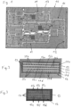
- the printed circuit board 10 generally can be an end product PCB 11 or, like in Figure 1 , an intermediate product comprising any number, here three, of end product PCBs 11.
- the printed circuit board 10 is composed of an isolating substrate 13 and conductive traces provided on one or both sides of the substrate 13, which is known per se in the art.
- the printed circuit board 10 comprises at least one solder wetting indicator 12, preferably a plurality of solder wetting indicators 12. Although Figure 1 shows only one solder wetting indicator 12, the printed circuit board 10 preferably comprises at least one solder wetting indicator 12 on each side of the printed circuit board 10.
- the or any solder wetting indicator 12 can be arranged in a margin region and/or in a waste area of the printed circuit board 10, like in Figure 1 , which is waste after the end product PCBs 11 have been cut out of the printed circuit board 10.
- At least one solder wetting indicator 12 can be arranged on any end product PCB 11. This has an advantage of traceability, because the quality of the soldering at the production can be attested over the lifetime of the end product PCB 11.
- the or any solder wetting indicator 12 comprises a solder pattern 14 arranged on the substrate 13.
- the solder pattern 14 comprises small solder volume deposits 15a-15f arranged in one or more lines on the substrate 13.
- the embodiment of Figure 3 comprises small solder volume deposits 15a-15f arranged in, for example, six parallel lines, i.e., small solder volume deposits 15a arranged in a first line, small solder volume deposits 15b arranged in a second line parallel to the first line, small solder volume deposits 15c arranged in a third line parallel to the first and second line, etc.
- the number of lines with small solder volume deposits 15a-15e can be different from six and generally can be any integer number equal to or greater than one, where the most preferred number of lines of small solder volume deposits 15a-15d is four, as shown in Figures 4 and 5 , as the optimum compromise between precision and space requirements of the solder wetting indicator 12.
- the small solder volume deposits 15a-15e are preferably applied or printed on corresponding conductive lines or pads 16a-16d provided on the substrate 13, see Figure 2 .
- the conductive lines 16a-16d are part of the conductive traces which are for example made of Copper.
- the conductive lines 16a-16d are preferably stripes of a certain length, preferably electrically isolated from each other, and preferably electrically isolated from all other conductive traces on the substrate 13, in order not to interfere with the electric circuitry of the printed circuit board 10.
- the small solder volume deposits 15a-15f are preferably arranged with monotonically increasing or decreasing distances relative to each other.
- the small solder volume deposits 15a-15f in each line are arrange with decreasing distances from left to right.
- the small solder volume deposits 15a-15f in a line can be arranged with logarithmically varying distances.
- solder wetting indicator 12 may look as shown in Figure 2 . In the following, it is assumed that a solder wetting indicator 12 is provided on both sides of the printed circuit board 10.
- the solder including the small solder volume deposits 15a-15f is applied to the printed circuit board 10.
- the solder wetting indicator 12 may look as shown in Figure 3 , where the small solder volume deposits 15a-15f are precisely positioned at their set position.
- the reflow step preferably comprises two passes, namely a first pass for curing or baking the first side of the printed circuit board 10, and a second pass for curing or baking the second side of the printed circuit board 10.
- the solder wetting indicator 12 may look as shown in Figure 4 or Figure 5 .
- the reflowing causes the small solder volume deposits 15a-15d to run along the conductive lines 16 (sideways in Figures 2-5 ), thus smearing out and possibly creating solder bridges 17 between adjacent small solder volume deposits 15a-15d of the same line.
- This bridging behavior relates to the wetting quality of the solder.
- the printed circuit board 10 comprises an offset indication pattern 19 indicating the set positions of the small solder volume deposits 15a-15d is provided. More specifically, the offset indication pattern 19 comprises offset indication lines 20a-20d, where each offset indication line 20a-20d corresponds to, and is arranged next to, a line of small solder volume deposits 15a-15d, resulting in an alternating arrangement of small solder volume deposit lines 15a-15d and offset indication lines 20a-20d, as visible in Figure 2 . Each offset indication line 20a-20d comprises offset indication spots 21a-21d indicating the set position of the small solder volume deposits 15a-15d along the corresponding line of small solder volume deposits 15a-15d.
- the offset indication lines 20a-20d are made of conductive traces on the substrate 13.
- the offset indication spots 21a-21d can be formed by spots of conductive traces, or, as in Figure 2 , by voids between conductive traces, which is an inverted scheme.
- the offset indication spots 21a-21d greatly facilitate the inspection of the small solder volume deposits 15a-15d after curing or baking relative to their set position, which could otherwise be difficult particularly in cases like in Figure 5 , where there is little information of the initial position of the small solder volume deposits 15a-15d left in the final pattern.
- the offset indication spots 21a-21d show indicate where the gaps between the small solder volume deposits 15a-15d were initially (before the reflow). Thus the number of bridges 17 can be easily counted and judged.
- some or all lines of small solder volume deposits 15a-15f have the small solder volume deposits 15a-15f arranged with differently varying distances from each other.
- the small solder volume deposits 15b are arranged with slightly larger distances from each other than the small solder volume deposits 15a
- the small solder volume deposits 15c are arranged with slightly larger distances from each other than the small solder volume deposits 15b
- the small solder volume deposits 15d are arranged with slightly larger distances from each other than the small solder volume deposits 15c. This feature allows for a more quantitative statement about the soldering quality.
Landscapes
- Engineering & Computer Science (AREA)
- Microelectronics & Electronic Packaging (AREA)
- Manufacturing & Machinery (AREA)
- Electric Connection Of Electric Components To Printed Circuits (AREA)
Abstract
A printed circuit board (10) comprises a substrate (13) and circuit traces provided on the substrate (13). The printed circuit board (10) comprises a solder wetting indicator (12). The solder wetting indicator (12) comprises a solder pattern (14) arranged on the substrate (13). The solder pattern (14) comprises small solder volume deposits (15a-15f) arranged along at least one line and having varying distances from each other.
Description
- The invention relates to a printed circuit board comprising a substrate and circuit traces provided on the substrate, and a method of determining the solder wetting quality of a printed circuit board.
- The solderability of printed circuit boards or PCBs is a quality issue. Process variations at the PCB supplier, shipment and storage can have a significant effect on the solderability on the plated solder pads.
- The problem underlying the present invention is to provide a printed circuit board and a method enabling simple and cost-effective determination of the solder wetting quality of the printed circuit board.
- The invention solves this problem with the features of the independent claims.
- According to the invention, the printed circuit board comprises a solder wetting indicator, wherein the solder wetting indicator comprises a solder pattern arranged on the substrate wherein the solder pattern comprises small solder volume deposits arranged along at least one line and having varying distances from each other. The small solder volume deposits can be for example solder spots, but not limited to these. Generally, the reflowing causes the small solder volume deposits of the solder wetting indicator to run along each corresponding line of small solder volume deposits, thus reaching out and possibly fusing with, and creating solder bridges between, adjacent small solder volume deposits of the same line. This bridging behavior relates to the wetting quality of the solder, where the number of solder bridges generally correlates with the solder wetting quality. Generally, a short or bridge between adjacent small solder volume deposits means good wetting. The more shorts and coalescence in-between the solder paste, the better the reflow and solder process. Therefore, the inventive solder wetting indicator provides a simple and cost-effective possibility for determining the solder quality of every printed circuit board in production, and also the plating quality by the PCB supplier. The performance of each PCB can be documented and compared during running of production.
- Preferably the solder pattern comprises small solder volume deposits arranged along a plurality of lines. Preferably the small solder volume deposits of the or each line are applied on a corresponding conductive line or pad provided on the substrate. Preferably the small solder volume deposits of some or all lines have differently varying distances from each other as compared to the small solder volume deposits of some or all other lines of small solder volume deposits. Preferably the lines of small solder volume deposits are arranged parallel to each other. The number of lines with small solder volume deposits in the solder wetting indicator generally can be any integer number equal to or greater than one, where the most preferred number of lines of small solder volume deposits is four, as an optimal compromise between precision and space requirements of the solder wetting indicator. Preferably, the small solder volume deposits in a line are arranged at least partly with monotonically increasing or decreasing, preferably logarithmically varying, distances. The solder wetting indicator can be customized with different solder paste patterns based on surface finish (Tin, Silver, Gold) offered by the PCB fabricator.
- At least one solder wetting indicator is preferably provided on both sides of the printed circuit board. In an embodiment of the invention, the solder wetting indicator is arranged in a margin region and/or a waste area of the printed circuit board. In this case, after the end product PCBs have been cut out of the printed circuit board, the solder wetting indicator is waste and can be disposed of. Alternatively, at least one solder wetting indicator can be arranged on every end product PCB. This has an advantage of traceability, because the individual quality of the soldering at the production can be attested over the lifetime of every end product PCB.
- The inventive solder wetting indicator allows for a simple visual detection of poor solder wetting quality cause by one or more of: the PCB being out of date; solder oven temperature profile issues; inferior PCB quality; solder paste issues; incorrect transport and storage conditions or shelf-life of the PCB and/or the solder paste, etc. Rapid detection of suspicious materials is possible. Furthermore, a comparison of the primary side vs. the secondary side process results is possible through the inventive solder wetting indicator. In addition to the PCB quality, the solder wetting indicator also reveals the solder paste performance and the surface mount technology (SMT) process setup. Also possible is a comparison of PCBs from different sources or alternative PCB suppliers. The solder wetting indicator can be used to evaluate and benchmark new solder paste chemistries with respect to flux performance, which is a key factor for soldering.
- In a preferred embodiment, the solder wetting indicator comprises an offset indication pattern arranged in a positional relationship to the (primary) solder pattern and indicating the set positions of the small solder volume deposits on the substrate before reflow. For better visibility, the offset indication pattern itself is preferably free of solder deposit. Preferably, the offset indication pattern comprises one or more offset indication lines, wherein the or each offset indication line is arranged in parallel to a corresponding line of small solder volume deposits. In other words, each offset indication line corresponds to, and is arranged next to, a line of small solder volume deposits, resulting in an alternating arrangement of small solder volume deposit lines and offset indication lines. Each offset indication line preferably comprises offset indication spots indicating the set position of the small solder volume deposits along the corresponding line of small solder volume deposits. Generally, the offset indication pattern greatly facilitates the inspection of the small solder volume deposits after curing or baking relative to their set position.
- The offset indication lines thus correspond to the varying gaps between the small solder volume deposits on the (primary) wetting indicator lines, namely, the gaps between the small solder volume deposits before they are reflow soldered. The offset indication lines facilitate an inspection of what gap lengths wetted as individual solder volume deposits coalesced together.
- Preferably the offset indication pattern is made of circuit traces provided on the substrate. In this case, the offset indication spots can be formed by spots of conductive traces, or by voids between conductive traces.
- According to a further aspect of the invention, a method of producing a printed circuit board is provided, comprising the steps of: providing a printed circuit board with a substrate, circuit traces provided on the substrate, and a solder wetting indicator, wherein the solder wetting indicator comprises a solder pattern arranged on the substrate, wherein the solder pattern comprises small solder volume deposits arranged along at least one line and having varying distances from each other; subjecting the printed circuit board to a reflow process; counting the number of bridges between adjacent small solder volume deposits in a line by human inspection or an automatic inspection device; and determining the solder wetting quality depending on the number of bridges counted. By counting the number of solder bridges between the small solder volume deposits after reflow, a quantitative indication of the solder wetting quality is obtained. The analysis can be done by a human or with an inspection device, for example an optical inspection device.
- The determination of the solder wetting quality advantageously can be used in different ways. In one embodiment, for example, machine parameters of a machine for producing printed circuit boards are adjusted depending on the determined solder wetting quality. In another embodiment, parameters of a reflow oven for heating, curing or baking printed circuit boards in the production process are adjusted depending on the determined solder wetting quality. In other words, the reflow oven profile settings can be re-adjusted based on the determined solder wetting quality, showing quantified solder results for the first side and second side reflow passes. Since the PCB properties can change from curing or baking the first side (pass 1) to curing or baking the second side (pass 2), the solder wetting indicator can look different on the two side of the printed circuit board, for example having different scales (distances between the small solder volume deposits). The solder wetting indicator can thus be used to fine tune and optimize the reflow oven settings. In this manner, the solderability can advantageously be ensured until the final pass of reflow soldering, where, generally, higher complexity, advanced electronic components are mounted and connected.
- After all, the inventive solder wetting indicator can be used for volume production setup and control.
- In the following the invention shall be illustrated on the basis of preferred embodiments with reference to the accompanying drawings, wherein:
- Fig. 1
- shows a plane view onto a printed circuit board; and
- Figs. 2-5
- show plane views on a solder wetting indicator at different times in the production process.
- The printed
circuit board 10 generally can be anend product PCB 11 or, like inFigure 1 , an intermediate product comprising any number, here three, ofend product PCBs 11. The printedcircuit board 10 is composed of anisolating substrate 13 and conductive traces provided on one or both sides of thesubstrate 13, which is known per se in the art. The printedcircuit board 10 comprises at least onesolder wetting indicator 12, preferably a plurality ofsolder wetting indicators 12. AlthoughFigure 1 shows only onesolder wetting indicator 12, the printedcircuit board 10 preferably comprises at least onesolder wetting indicator 12 on each side of the printedcircuit board 10. - The or any
solder wetting indicator 12 can be arranged in a margin region and/or in a waste area of the printedcircuit board 10, like inFigure 1 , which is waste after theend product PCBs 11 have been cut out of the printedcircuit board 10. - Alternatively, at least one
solder wetting indicator 12 can be arranged on any end product PCB 11. This has an advantage of traceability, because the quality of the soldering at the production can be attested over the lifetime of theend product PCB 11. - The or any
solder wetting indicator 12 comprises asolder pattern 14 arranged on thesubstrate 13. Thesolder pattern 14 comprises smallsolder volume deposits 15a-15f arranged in one or more lines on thesubstrate 13. The embodiment ofFigure 3 comprises smallsolder volume deposits 15a-15f arranged in, for example, six parallel lines, i.e., smallsolder volume deposits 15a arranged in a first line, small solder volume deposits 15b arranged in a second line parallel to the first line, smallsolder volume deposits 15c arranged in a third line parallel to the first and second line, etc. The number of lines with smallsolder volume deposits 15a-15e can be different from six and generally can be any integer number equal to or greater than one, where the most preferred number of lines of smallsolder volume deposits 15a-15d is four, as shown inFigures 4 and 5 , as the optimum compromise between precision and space requirements of thesolder wetting indicator 12. - The small
solder volume deposits 15a-15e are preferably applied or printed on corresponding conductive lines orpads 16a-16d provided on thesubstrate 13, seeFigure 2 . Theconductive lines 16a-16d are part of the conductive traces which are for example made of Copper. Theconductive lines 16a-16d are preferably stripes of a certain length, preferably electrically isolated from each other, and preferably electrically isolated from all other conductive traces on thesubstrate 13, in order not to interfere with the electric circuitry of the printedcircuit board 10. - Within each line the small
solder volume deposits 15a-15f are preferably arranged with monotonically increasing or decreasing distances relative to each other. For example, inFigure 3 the smallsolder volume deposits 15a-15f in each line are arrange with decreasing distances from left to right. More specifically, the smallsolder volume deposits 15a-15f in a line can be arranged with logarithmically varying distances. The above features allow a more quantitative statement about the soldering quality, as will be explained below. - The process of generating and evaluating the at least one
solder wetting indicator 12 is explained in the following on the basis of the enclosed Figures. - First of all, a printed
circuit board 10 is provided in a pre-soldering condition, i.e., still without solder. In this state, thesolder wetting indicator 12 may look as shown inFigure 2 . In the following, it is assumed that asolder wetting indicator 12 is provided on both sides of the printedcircuit board 10. - In the next step, the solder including the small
solder volume deposits 15a-15f is applied to the printedcircuit board 10. After this step, thesolder wetting indicator 12 may look as shown inFigure 3 , where the smallsolder volume deposits 15a-15f are precisely positioned at their set position. - Then at least one step of curing or baking, also called reflowing, is applied to the printed
circuit board 10 for example in an oven. Usually, one side of the PCB is cured or baked at a time. Therefore, in the present embodiment, where asolder wetting indicator 12 is provided on both sides of the printedcircuit board 10, the reflow step preferably comprises two passes, namely a first pass for curing or baking the first side of the printedcircuit board 10, and a second pass for curing or baking the second side of the printedcircuit board 10. - After the reflowing step, the
solder wetting indicator 12 may look as shown inFigure 4 or Figure 5 . Generally, the reflowing causes the smallsolder volume deposits 15a-15d to run along the conductive lines 16 (sideways inFigures 2-5 ), thus smearing out and possibly creatingsolder bridges 17 between adjacent smallsolder volume deposits 15a-15d of the same line. This bridging behavior relates to the wetting quality of the solder. InFigure 4 , there are only four solder bridges, and very little spread of the smallsolder volume deposits 15a-15d caused by the reflow. Therefore, inspection of the wettingindicator 12 would yield an estimation of high wetting angles, and low or poor wetting. - In
Figure 5 , in contrast, forty-eightsolder bridges 17 can be counted, and extended spreading out of the smallsolder volume deposits 15a-15d to the indicator edge to the right, caused by the reflow, is observed. Therefore, inspection of the wettingindicator 12 would yield an estimation of low wetting angles, and excellent solder wetting. - Summarizing the above, by counting the number of solder bridges 17 between the small
solder volume deposits 15a-15d after reflow, a quantitative indication of the solder wetting quality is obtained. - In a preferred embodiment shown in
Figure 2 , the printedcircuit board 10 comprises an offsetindication pattern 19 indicating the set positions of the smallsolder volume deposits 15a-15d is provided. More specifically, the offsetindication pattern 19 comprises offsetindication lines 20a-20d, where each offsetindication line 20a-20d corresponds to, and is arranged next to, a line of smallsolder volume deposits 15a-15d, resulting in an alternating arrangement of small soldervolume deposit lines 15a-15d and offsetindication lines 20a-20d, as visible inFigure 2 . Each offsetindication line 20a-20d comprises offset indication spots 21a-21d indicating the set position of the smallsolder volume deposits 15a-15d along the corresponding line of smallsolder volume deposits 15a-15d. Preferably, the offsetindication lines 20a-20d are made of conductive traces on thesubstrate 13. In this case, the offset indication spots 21a-21d can be formed by spots of conductive traces, or, as inFigure 2 , by voids between conductive traces, which is an inverted scheme. The offset indication spots 21a-21d greatly facilitate the inspection of the smallsolder volume deposits 15a-15d after curing or baking relative to their set position, which could otherwise be difficult particularly in cases like inFigure 5 , where there is little information of the initial position of the smallsolder volume deposits 15a-15d left in the final pattern. In other words, the offset indication spots 21a-21d show indicate where the gaps between the smallsolder volume deposits 15a-15d were initially (before the reflow). Thus the number ofbridges 17 can be easily counted and judged. - As can be seen for example in
Figures 2 and4 , some or all lines of smallsolder volume deposits 15a-15f have the smallsolder volume deposits 15a-15f arranged with differently varying distances from each other. For example, inFigure 2 , the small solder volume deposits 15b are arranged with slightly larger distances from each other than the smallsolder volume deposits 15a, the smallsolder volume deposits 15c are arranged with slightly larger distances from each other than the small solder volume deposits 15b, and the smallsolder volume deposits 15d are arranged with slightly larger distances from each other than the smallsolder volume deposits 15c. This feature allows for a more quantitative statement about the soldering quality.
Claims (14)
- A printed circuit board (10) comprising a substrate (13) and circuit traces provided on the substrate (13), characterized in that the printed circuit board (10) comprises a solder wetting indicator (12), wherein the solder wetting indicator (12) comprises a solder pattern (14) arranged on the substrate (13), wherein the solder pattern (14) comprises small solder volume deposits (15a-15f) arranged along at least one line and having varying distances from each other.
- The printed circuit board (10) as claimed in claim 1,
wherein the solder pattern (14) comprises small solder volume deposits (15a-15f) arranged along a plurality of lines. - The printed circuit board (10) as claimed in claim 2,
wherein the small solder volume deposits (15a-15f) of some or all lines have differently varying distances from each other as compared to the small solder volume deposits of some or all other lines of small solder volume deposits (15a-15f). - The printed circuit board (10) as claimed in claim 2 or 3, wherein the lines of small solder volume deposits (15a-15f) are arranged parallel to each other.
- The printed circuit board (10) as claimed in any one of claims 2 to 4, wherein the solder pattern (14) comprises four lines of small solder volume deposits (15a-15d).
- The printed circuit board (10) as claimed in any one of the preceding claims, wherein the small solder volume deposits (15a-15e) of the or each line are applied on a corresponding conductive line (16a-16d) provided on the substrate (13).
- The printed circuit board (10) as claimed in any one of the preceding claims, wherein the solder wetting indicator (12) is arranged in a margin region and/or a waste area of the printed circuit board (10).
- The printed circuit board (10) as claimed in any one of the preceding claims, wherein the small solder volume deposits (15a-15f) in a line are arranged at least partly with monotonically increasing or decreasing, preferably logarithmically varying, distances.
- The printed circuit board (10) as claimed in any one of the preceding claims, wherein the solder wetting indicator (12) comprises an offset indication pattern (19) arranged in a positional relationship to the solder pattern (14) and indicating the set positions of the small solder volume deposits (15a-15d) on the substrate (13) before reflow.
- The printed circuit board (10) as claimed in claim 9,
wherein the offset indication pattern (19) comprises one or more offset indication lines (20a-20d), wherein the or each offset indication line (20a-20d) is arranged in parallel to a corresponding line of small solder volume deposits (15a-15d). - The printed circuit board (10) as claimed in claim 9 or 10, wherein the offset indication pattern (19) is made of circuit traces provided on the substrate (13).
- A method of determining the solder wetting quality of a printed circuit board (10), comprising the steps of:- providing a printed circuit board (10) with a substrate (13), circuit traces provided on the substrate (13), and a solder wetting indicator (12), wherein the solder wetting indicator (12) comprises a solder pattern (14) arranged on the substrate (13), wherein the solder pattern (14) comprises small solder volume deposits (15a-15f) arranged along at least one line and having varying distances from each other;- subjecting the printed circuit board (10) to a reflow process;- counting the number of bridges (17) between adjacent small solder volume deposits (15a-15d) in a line by human inspection or an automatic inspection device; and- determining the solder wetting quality depending on the number of bridges (17) counted.
- The method as claimed in claim 12, wherein machine parameters of a machine for producing printed circuit boards (10) are adjusted depending on the determined solder wetting quality.
- The method as claimed in claim 12 or 13, wherein parameters of a reflow oven for heating printed circuit boards in the production process are adjusted depending on the determined solder wetting quality.
Priority Applications (1)
| Application Number | Priority Date | Filing Date | Title |
|---|---|---|---|
| EP23153093.2A EP4408129A1 (en) | 2023-01-24 | 2023-01-24 | Printed circuit board and method of determining the solder wetting quality of a printed circuit board |
Applications Claiming Priority (1)
| Application Number | Priority Date | Filing Date | Title |
|---|---|---|---|
| EP23153093.2A EP4408129A1 (en) | 2023-01-24 | 2023-01-24 | Printed circuit board and method of determining the solder wetting quality of a printed circuit board |
Publications (1)
| Publication Number | Publication Date |
|---|---|
| EP4408129A1 true EP4408129A1 (en) | 2024-07-31 |
Family
ID=85076498
Family Applications (1)
| Application Number | Title | Priority Date | Filing Date |
|---|---|---|---|
| EP23153093.2A Pending EP4408129A1 (en) | 2023-01-24 | 2023-01-24 | Printed circuit board and method of determining the solder wetting quality of a printed circuit board |
Country Status (1)
| Country | Link |
|---|---|
| EP (1) | EP4408129A1 (en) |
Citations (2)
| Publication number | Priority date | Publication date | Assignee | Title |
|---|---|---|---|---|
| GB2183189A (en) * | 1985-11-08 | 1987-06-03 | Sony Corp | Printed circuit boards |
| JPH05191034A (en) * | 1992-01-17 | 1993-07-30 | Sharp Corp | Printed wiring board fabricated by reflow |
-
2023
- 2023-01-24 EP EP23153093.2A patent/EP4408129A1/en active Pending
Patent Citations (2)
| Publication number | Priority date | Publication date | Assignee | Title |
|---|---|---|---|---|
| GB2183189A (en) * | 1985-11-08 | 1987-06-03 | Sony Corp | Printed circuit boards |
| JPH05191034A (en) * | 1992-01-17 | 1993-07-30 | Sharp Corp | Printed wiring board fabricated by reflow |
Similar Documents
| Publication | Publication Date | Title |
|---|---|---|
| US20170280565A1 (en) | Jumpers for pcb design and assembly | |
| US20150373886A1 (en) | Integral heater assembly and method for host board of electronic package assembly | |
| EP2012571A2 (en) | Connection structure between printed circuit board and electronic component | |
| US20100025090A1 (en) | Printed substrate through which very strong currents can pass and corresponding production method | |
| US7129814B2 (en) | Chip resistor and method of making the same | |
| US9635754B2 (en) | Circuit assembly | |
| Härter et al. | Comprehensive correlation of inline inspection data for the evaluation of defects in heterogeneous electronic assemblies | |
| JPS62109396A (en) | Printed circuit substrate | |
| US6333471B1 (en) | Sheet metal component for double pattern conduction and printed circuit board | |
| US20050281007A1 (en) | Heat management in circuit card assemblies | |
| AU2013201130B2 (en) | Printed circuit board | |
| US6054720A (en) | Apparatus and method for evaluating the surface insulation resistance of electronic assembly manufacture | |
| EP2280593B1 (en) | Fluxometer system and method | |
| KR20190058228A (en) | Wave jig that can prevent overheating of pcb during wave soldering process and wave soldering method using the same | |
| KR101094411B1 (en) | 4 terminal type printed circuit board inspection method | |
| EP0245713B1 (en) | Solder pads for use on printed circuit boards | |
| CN110849250B (en) | A device for detecting flatness of pins of patch components | |
| CN210225918U (en) | Carbon oil plate | |
| KR20040107433A (en) | Circuit board having resistor and method for manufacturing the circuit board | |
| JP2009224697A (en) | Printed circuit board and electronic component mounting substrate | |
| Zarrow | Reflow soldering of through-hole components | |
| JP7197393B2 (en) | Sulfurization detection sensor and manufacturing method thereof | |
| CN209710425U (en) | A kind of Novel PCB board | |
| KR101128146B1 (en) | Printed Circuit Board | |
| CN118571583A (en) | Design processing method of embedded resistor printed board resistor |
Legal Events
| Date | Code | Title | Description |
|---|---|---|---|
| PUAI | Public reference made under article 153(3) epc to a published international application that has entered the european phase |
Free format text: ORIGINAL CODE: 0009012 |
|
| STAA | Information on the status of an ep patent application or granted ep patent |
Free format text: STATUS: THE APPLICATION HAS BEEN PUBLISHED |
|
| AK | Designated contracting states |
Kind code of ref document: A1 Designated state(s): AL AT BE BG CH CY CZ DE DK EE ES FI FR GB GR HR HU IE IS IT LI LT LU LV MC ME MK MT NL NO PL PT RO RS SE SI SK SM TR |
|
| STAA | Information on the status of an ep patent application or granted ep patent |
Free format text: STATUS: REQUEST FOR EXAMINATION WAS MADE |
|
| 17P | Request for examination filed |
Effective date: 20250129 |