EP4407697A2 - Lichtemittierendes element für eine anzeige - Google Patents
Lichtemittierendes element für eine anzeige Download PDFInfo
- Publication number
- EP4407697A2 EP4407697A2 EP24169073.4A EP24169073A EP4407697A2 EP 4407697 A2 EP4407697 A2 EP 4407697A2 EP 24169073 A EP24169073 A EP 24169073A EP 4407697 A2 EP4407697 A2 EP 4407697A2
- Authority
- EP
- European Patent Office
- Prior art keywords
- led stack
- type semiconductor
- conductivity type
- led
- light emitting
- Prior art date
- Legal status (The legal status is an assumption and is not a legal conclusion. Google has not performed a legal analysis and makes no representation as to the accuracy of the status listed.)
- Pending
Links
Images
















Classifications
-
- H—ELECTRICITY
- H10—SEMICONDUCTOR DEVICES; ELECTRIC SOLID-STATE DEVICES NOT OTHERWISE PROVIDED FOR
- H10W—GENERIC PACKAGES, INTERCONNECTIONS, CONNECTORS OR OTHER CONSTRUCTIONAL DETAILS OF DEVICES COVERED BY CLASS H10
- H10W90/00—Package configurations
-
- G—PHYSICS
- G09—EDUCATION; CRYPTOGRAPHY; DISPLAY; ADVERTISING; SEALS
- G09F—DISPLAYING; ADVERTISING; SIGNS; LABELS OR NAME-PLATES; SEALS
- G09F9/00—Indicating arrangements for variable information in which the information is built-up on a support by selection or combination of individual elements
- G09F9/30—Indicating arrangements for variable information in which the information is built-up on a support by selection or combination of individual elements in which the desired character or characters are formed by combining individual elements
- G09F9/33—Indicating arrangements for variable information in which the information is built-up on a support by selection or combination of individual elements in which the desired character or characters are formed by combining individual elements being semiconductor devices, e.g. diodes
-
- H—ELECTRICITY
- H10—SEMICONDUCTOR DEVICES; ELECTRIC SOLID-STATE DEVICES NOT OTHERWISE PROVIDED FOR
- H10H—INORGANIC LIGHT-EMITTING SEMICONDUCTOR DEVICES HAVING POTENTIAL BARRIERS
- H10H20/00—Individual inorganic light-emitting semiconductor devices having potential barriers, e.g. light-emitting diodes [LED]
- H10H20/80—Constructional details
- H10H20/81—Bodies
-
- H—ELECTRICITY
- H10—SEMICONDUCTOR DEVICES; ELECTRIC SOLID-STATE DEVICES NOT OTHERWISE PROVIDED FOR
- H10H—INORGANIC LIGHT-EMITTING SEMICONDUCTOR DEVICES HAVING POTENTIAL BARRIERS
- H10H20/00—Individual inorganic light-emitting semiconductor devices having potential barriers, e.g. light-emitting diodes [LED]
- H10H20/80—Constructional details
- H10H20/81—Bodies
- H10H20/813—Bodies having a plurality of light-emitting regions, e.g. multi-junction LEDs or light-emitting devices having photoluminescent regions within the bodies
-
- H—ELECTRICITY
- H10—SEMICONDUCTOR DEVICES; ELECTRIC SOLID-STATE DEVICES NOT OTHERWISE PROVIDED FOR
- H10H—INORGANIC LIGHT-EMITTING SEMICONDUCTOR DEVICES HAVING POTENTIAL BARRIERS
- H10H20/00—Individual inorganic light-emitting semiconductor devices having potential barriers, e.g. light-emitting diodes [LED]
- H10H20/80—Constructional details
- H10H20/81—Bodies
- H10H20/819—Bodies characterised by their shape, e.g. curved or truncated substrates
-
- H—ELECTRICITY
- H10—SEMICONDUCTOR DEVICES; ELECTRIC SOLID-STATE DEVICES NOT OTHERWISE PROVIDED FOR
- H10H—INORGANIC LIGHT-EMITTING SEMICONDUCTOR DEVICES HAVING POTENTIAL BARRIERS
- H10H20/00—Individual inorganic light-emitting semiconductor devices having potential barriers, e.g. light-emitting diodes [LED]
- H10H20/80—Constructional details
- H10H20/83—Electrodes
- H10H20/831—Electrodes characterised by their shape
-
- H—ELECTRICITY
- H10—SEMICONDUCTOR DEVICES; ELECTRIC SOLID-STATE DEVICES NOT OTHERWISE PROVIDED FOR
- H10H—INORGANIC LIGHT-EMITTING SEMICONDUCTOR DEVICES HAVING POTENTIAL BARRIERS
- H10H20/00—Individual inorganic light-emitting semiconductor devices having potential barriers, e.g. light-emitting diodes [LED]
- H10H20/80—Constructional details
- H10H20/83—Electrodes
- H10H20/831—Electrodes characterised by their shape
- H10H20/8312—Electrodes characterised by their shape extending at least partially through the bodies
-
- H—ELECTRICITY
- H10—SEMICONDUCTOR DEVICES; ELECTRIC SOLID-STATE DEVICES NOT OTHERWISE PROVIDED FOR
- H10H—INORGANIC LIGHT-EMITTING SEMICONDUCTOR DEVICES HAVING POTENTIAL BARRIERS
- H10H20/00—Individual inorganic light-emitting semiconductor devices having potential barriers, e.g. light-emitting diodes [LED]
- H10H20/80—Constructional details
- H10H20/83—Electrodes
- H10H20/832—Electrodes characterised by their material
- H10H20/833—Transparent materials
-
- H—ELECTRICITY
- H10—SEMICONDUCTOR DEVICES; ELECTRIC SOLID-STATE DEVICES NOT OTHERWISE PROVIDED FOR
- H10H—INORGANIC LIGHT-EMITTING SEMICONDUCTOR DEVICES HAVING POTENTIAL BARRIERS
- H10H20/00—Individual inorganic light-emitting semiconductor devices having potential barriers, e.g. light-emitting diodes [LED]
- H10H20/80—Constructional details
- H10H20/85—Packages
- H10H20/857—Interconnections, e.g. lead-frames, bond wires or solder balls
Definitions
- Exemplary embodiments relate to a light emitting device for a display and a display apparatus, and, more particularly, to a light emitting device having a stack structure of a plurality of LEDs for a display, and a display apparatus including the same.
- light emitting diodes As an inorganic light source, light emitting diodes have been used in various technical fields, such as displays, vehicular lamps, general lighting, and the like. With various advantages of the light emitting diodes, such as longer lifespan, lower power consumption, and faster response, than existing light sources, light emitting diodes have been replacing the existing light sources.
- Light emitting diodes have been generally used as backlight light sources in display apparatuses.
- LED displays that directly realize images using the light emitting diodes have been recently developed.
- a display apparatus displays various colors through mixture of blue, green, and red light.
- the display apparatus includes a plurality of pixels, each including sub-pixels corresponding to one of blue, green, and red light.
- a color of a certain pixel is typically determined based on the colors of the sub-pixels, so that images can be realized through the combination of such pixels.
- LEDs can emit various colors depending upon materials thereof, individual LED chips emitting blue, green and red light may be arranged on a two-dimensional plane to provide a display apparatus. However, when one LED chip is provided to each sub-pixel, the number of LED chips may be increased, which may require excessive time for a mounting process during manufacture.
- each subpixel must be reduced in order to arrange the subpixels in a restricted area.
- reduction in the area of the LED chip may cause difficulties in mounting the LED chip and reduction in a luminous area.
- Exemplary embodiments provide a light emitting device for a display that is capable of increasing an area of each sub-pixel in a restricted pixel area and a display apparatus including the same.
- Exemplary embodiments also provide a light emitting device for a display that is capable of reducing a time associated with a mounting process and a display apparatus including the same.
- Exemplary embodiments further provide a light emitting device for a display that is capable of increasing the production yield and a display apparatus including the same.
- An exemplary embodiment of the present disclosure provides a light emitting device for a display including: a first LED stack; a second LED stack disposed under the first LED stack; a third LED stack disposed under the second LED stack; a first transparent electrode interposed between the first LED stack and the second LED stack, and being in ohmic contact with a lower surface of the first LED stack; a second transparent electrode interposed between the first LED stack and the second LED stack, and being in ohmic contact with an upper surface of the second LED stack; a third transparent electrode interposed between the second LED stack and the third LED stack, and being in ohmic contact with an upper surface of the third LED stack; an n electrode pad disposed on a first conductivity type semiconductor layer of the third LED stack; a lower p electrode pad disposed on the third transparent electrode; and bump pads disposed on the first LED stack, wherein each of the first to third LED stacks includes a first conductivity type semiconductor layer, an active layer and a second conductivity type semiconductor layer, the bump pads include first to third bump pads and
- An exemplary embodiment of the present disclosure provides a light emitting device for a display including: a first LED stack; a second LED stack disposed under the first LED stack; a third LED stack disposed under the second LED stack; a first transparent electrode interposed between the first LED stack and the second LED stack, and being in ohmic contact with a lower surface of the first LED stack; a second transparent electrode interposed between the first LED stack and the second LED stack, and being in ohmic contact with an upper surface of the second LED stack; a third transparent electrode interposed between the second LED stack and the third LED stack, and being in ohmic contact with an upper surface of the third LED stack; bump pads disposed on the first LED stack, wherein each of the first to third LED stacks includes a first conductivity type semiconductor layer, an active layer and a second conductivity type semiconductor layer, and at least one of the first to third transparent electrodes is recessed from an edge of the second conductivity type semiconductor layer of the first to third LED stacks.
- Embodiments of the present disclosure provide a display apparatus including: a circuit board; and a plurality of light emitting devices arranged on the circuit board, wherein each of the light emitting devices is the light emitting device set forth above, and the electrode pads are electrically connected to the circuit board.
- a light emitting device for a display includes: a first LED stack; a second LED stack disposed under the first LED stack; a third LED stack disposed under the second LED stack; a first transparent electrode interposed between the first LED stack and the second LED stack, and being in ohmic contact with a lower surface of the first LED stack; a second transparent electrode interposed between the first LED stack and the second LED stack, and being in ohmic contact with an upper surface of the second LED stack; a third transparent electrode interposed between the second LED stack and the third LED stack, and being in ohmic contact with an upper surface of the third LED stack; an n electrode pad disposed on a first conductivity type semiconductor layer of the third LED stack; a lower p electrode pad disposed on the third transparent electrode; and bump pads disposed on the first LED stack, wherein each of the first to third LED stacks includes a first conductivity type semiconductor layer, an active layer and a second conductivity type semiconductor layer, the bump pads include first to third bump pads and common bump pads
- the second LED stack is disposed under the first LED stack
- the third LED stack is disposed under the second LED stack, but the light emitting device may be flip-bonded. Therefore, it should be noted that upper and lower positions of these first to third LED stacks may be reversed.
- the light emitting device may increase a luminous area of each subpixel without increasing a pixel area.
- the upper surface of the n electrode pad is set to be located at the same elevation as that of the lower p electrode pad, and thus damage to any one of these pads may be prevented.
- the first LED stack may emit light having a longer wavelength than that of the second LED stack, and the second LED stack may emit light having a longer wavelength than that of the third LED stack.
- the first, second and third LED stacks may emit red light, green light and blue light, respectively.
- the first LED stack may emit light having a longer wavelength than that of the third LED stack, and the second LED stack may emit light having a shorter wavelength than that of the third LED stack.
- the first, second and third LED stacks may emit red light, blue light and green light, respectively.
- the first to third LED stacks may be independently driven, light generated from the first LED stack may be emitted outside through the second LED stack and the third LED stack, and light generated from the second LED stack may be emitted outside through the third LED stack.
- any one of the first to third transparent electrodes may be formed of a material different from the remaining transparent electrodes.
- the first transparent electrode may be formed of indium-tin-oxide (ITO), and the second and third transparent electrodes may be formed of ZnO.
- each of the first to third transparent electrodes may contact the second conductivity type semiconductor layer, and the second and third transparent electrodes may be recessed to have a smaller area than that of the second conductivity type semiconductor layer of the second LED stack and that of the second conductivity type semiconductor layer of the third LED stack, respectively.
- the second and third transparent electrodes are recessed, and thus they may be prevented from being damaged by etching gas during the manufacturing process.
- the common bump pad may be commonly electrically connected to first conductivity type semiconductor layers of the first to third LED stacks, wherein the first to third bump pads may be electrically connected to second conductivity type semiconductor layers of first to third LED stacks, respectively.
- the common bump pad may be commonly electrically connected to the second conductivity type semiconductor layers of the first to third LED stacks, and the first to third bump pads may be electrically connected to the first conductivity type semiconductor layers of the third LED stacks, respectively.
- the light emitting device may further include an insulation layer covering side surfaces of the first to third LED stacks, wherein the side surfaces of the first to third LED stacks and a side surface of the first transparent electrode may be in contact with the insulation layer, and side surfaces of the second and third transparent electrodes may be spaced apart from the insulation layer.
- Side surfaces of the light emitting device may be inclined at a range of 75 degrees to 90 degrees with respect to the upper surface of the third LED stack.
- the inclination angle of the side surfaces of the light emitting device is set to 75 degrees or more, and thus a luminous area of the first LED stack may be secured.
- the light emitting device may further include a first bonding layer interposed between the second LED stack and the third LED stack; and a second bonding layer interposed between the first LED stack and the second LED stack.
- the light emitting device may further include lower through holes passing through the second LED stack and the first bonding layer to expose the n electrode pad and the lower p electrode pad, respectively; a lower common connector connected to the n electrode pad; and a lower p connector connected to the lower p electrode pad, wherein the lower common connector may be electrically connected to the first conductivity type semiconductor layer of the LED stack, and connected to the n electrode pad exposed through the lower through hole, and the lower p connector may be electrically connected to the lower p electrode pad exposed through the lower through hole.
- the light emitting device may further include an upper p electrode pad which is disposed on the second transparent electrode and electrically connected to the second conductivity type semiconductor layer of the second LED stack.
- the light emitting device may further include a through hole passing through the first LED stack to expose the first transparent electrode; through holes passing through the first LED stack, the first transparent electrode and the second bonding layer to expose the upper p electrode pad, the lower p connector, and the lower common connector, respectively; and first to third upper connectors and an upper common connector disposed on the first LED stack, and electrically connected to the first transparent electrode, the upper p electrode pad, the lower p connector, and the lower common connector through through holes passing through the first LED stack, wherein the bump pads may be disposed on the first to third upper connectors and the upper common connector, respectively.
- the bump pads may be located on flat portions of the first to third upper connectors and the upper common connector, respectively.
- the light emitting device may further include an upper insulation layer covering the first to third upper connectors and the upper common connector, wherein the upper insulation layer may have openings exposing the first to third upper connectors and the upper common connector, and each of the bump pads may be disposed in the openings.
- the light emitting device may further include an intermediate insulation layer disposed between the first LED stack and the upper connectors, wherein the intermediate insulation layer may cover a side surface of the light emitting device and a sidewall of the through hole passing through the first LED stack, and may include openings exposing the first transparent electrode, the upper p electrode pad, the lower p connector, and the lower common connector.
- the first to third LED stacks may be stacks separated from a growth substrate.
- the light emitting device does not have the growth substrate.
- a light emitting device for a display may include: a first LED stack; a second LED stack disposed under the first LED stack; a third LED stack disposed under the second LED stack; a first transparent electrode interposed between the first LED stack and the second LED stack, and being in ohmic contact with a lower surface of the first LED stack; a second transparent electrode interposed between the first LED stack and the second LED stack, and being in ohmic contact with an upper surface of the second LED stack; a third transparent electrode interposed between the second LED stack and the third LED stack, and being in ohmic contact with an upper surface of the third LED stack; bump pads disposed on the first LED stack, wherein each of the first to third LED stacks may include a first conductivity type semiconductor layer, an active layer and a second conductivity type semiconductor layer, and at least one of the first to third transparent electrodes may be recessed from an edge of the second conductivity type semiconductor layer of the first to third LED stacks.
- the light emitting device may further include an n electrode pad disposed on the first conductivity type semiconductor layer of the third LED stack; a lower p electrode pad disposed on the third transparent electrode, wherein an upper surface of the n electrode pad may be located at the same elevation as that of the lower p electrode pad.
- a display apparatus in accordance with one embodiment of the present disclosure includes: a circuit board; and a plurality of light emitting devices arranged on the circuit board, wherein each of the light emitting devices is the light emitting device set forth above and the bump pads are electrically connected to the circuit board.
- FIG. 1 shows schematic perspective views illustrating display apparatuses according to exemplary embodiments.
- the display apparatus may be used in a VR display apparatus, such as a smart watch 1000a or a VR headset 1000b, or an AR display apparatus, such as augmented reality glasses 1000c.
- a VR display apparatus such as a smart watch 1000a or a VR headset 1000b
- an AR display apparatus such as augmented reality glasses 1000c.
- the display apparatus may include a display panel for implementing an image.
- FIG. 2 is a schematic plan view illustrating the display panel according to an exemplary embodiment.
- the display panel includes a circuit board 101 and light emitting devices 100.
- the circuit board 101 may include a circuit for passive matrix driving or active matrix driving.
- the circuit board 101 may include interconnection lines and resistors.
- the circuit board 101 may include interconnection lines, transistors, and capacitors.
- the circuit board 101 may also have pads disposed on an upper surface thereof to allow electrical connection to the circuit therein.
- a plurality of light emitting devices 100 are arranged on the circuit board 101. Each of the light emitting devices 100 may form one pixel.
- the light emitting device 100 includes bump pads 73, and the bump pads 73 are electrically connected to the circuit board 101. For example, the bump pads 73 may be bonded to pads exposed on the circuit board 101.
- An interval between the light emitting devices 100 may be greater than at least a width of the light emitting device 100.
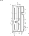
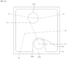
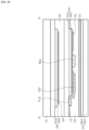
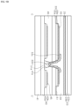
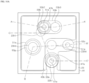
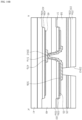
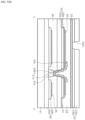
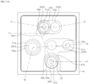
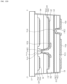
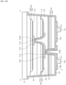
- FIG. 3A is a schematic plan view illustrating the light emitting device 100 according to an exemplary embodiment.
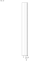
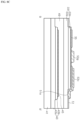
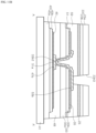
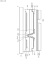
- FIG. 3B , FIG. 3C , and 3D are schematic cross-sectional views taken along the lines A-A', B-B', and C-C' of FIG. 3A , respectively.
- the bump pads 73r, 73b, 73g, and 73c are exemplarily illustrated and described as being disposed at an upper side in FIG. 3A to FIG. 3D , the inventive concepts are not limited thereto.
- the light emitting device 100 may be flip-bonded on the circuit board 101 shown in FIG. 2 , and in this case, the bump pads 73r, 73b, 73g, and 73c may be disposed at a lower side.
- the light emitting device 100 may include a first LED stack 23, a second LED stack 33, a third LED stack 43, a first transparent electrode 25, a second transparent electrode 35, a third transparent electrode 45, an n-electrode pad 47a, a lower p-electrode pad 47b, an upper p-electrode pad 53g, a lower p-connector 53b, a lower common connector 53c, an upper common connector 63c, a first upper connector 63r, a second upper connector 63g, a third upper connector 63b, a first bonding layer 49, a second bonding layer 59, a lower insulation layer 51, an intermediate insulation layer 61, an upper insulation layer 71, and bump pads 73a, 73b, 73c, and 73d.
- the light emitting device 100 may further include through holes 23h1, 23h2, 23h3, and 23h4 passing through the first LED stack
- the first, second, and third LED stacks 23, 33, and 43 are stacked in the vertical direction.
- the first, second, and third LED stacks 23, 33, and 43 may be grown on different growth substrates from each other, and according to the illustrated exemplary embodiment, each of the growth substrates may be removed from the final light emitting device 100.
- the light emitting device 100 does not include the growth substrates of the first, second, and third LED stacks 23, 33, and 43.
- the inventive concepts are not limited thereto, and in some exemplary embodiments, at least one of the growth substrates may be included in the light emitting device 100.
- Each of the first LED stack 23, the second LED stack 33 and the third LED stack 43 includes a first conductivity type semiconductor layer 23a, 33a, or 43a, a second conductivity type semiconductor layer 23b, 33b, or 43b, and an active layer interposed therebetween.
- the active layer may have a multiple quantum well structure, for example.
- the second LED stack 33 is disposed under the first LED stack 23, and the third LED stack 43 is disposed under the second LED stack 33. Light generated in the first to third LED stacks 23, 33, and 43 may be emitted to the outside through the third LED stack 43.
- the first LED stack 23 may emit light having a longer wavelength than those emitted from the second and third LED stacks 33 and 43, and the second LED stack 33 may emit light having a longer wavelength than that emitted from the third LED stack 43.
- the first LED stack 23 may be an inorganic light emitting diode emitting red light
- the second LED stack 33 may be an inorganic light emitting diode emitting green light
- the third LED stack 43 may be an inorganic light emitting diode to emitting blue light.
- the first LED stack 23 may include an AlGaInP-based well layer
- the second LED stack 33 may include an AlGaInP or AlGaInN-based well layer
- the third LED stack 43 may include an AlGaInN-based well layer.
- the first LED stack 23 emits light having a longer wavelength than those emitted from the second and third LED stacks 33 and 43, light generated from the first LED stack 23 may be emitted to the outside after passing through the second and third LED stacks 33 and 43.
- the second LED stack 33 emits light having a longer wavelength than that of emitted from the third LED stack 43, light generated from the second LED stack 33 may be emitted to the outside after passing through the third LED stack 43.
- the first LED stack 23 may emit light having a longer wavelength than those emitted from the second and third LED stacks 33 and 43, and the second LED stack 33 may emit light having a shorter wavelength than that emitted from the third LED stack 43.
- the first LED stack 23 may be an inorganic light emitting diode emitting red light
- the second LED stack 33 may be an inorganic light emitting diode emitting blue light
- the third LED stack 43 may be an inorganic light emitting diode emitting green light.
- the first LED stack 23 may include an AlGaInP-based well layer
- the second LED stack 33 may include an AlGaInN-based well layer
- the third LED stack 43 may include an AlGaInP-based or AlGaInN-based well layer.
- a portion of light generated in the second LED 33 stack may be absorbed in the third LED stack 43, and thus, luminous intensity of light emitted from the second LED stack 33 may be relatively lower than that of light emitted from the first or third LED stacks 23 or 43. Accordingly, a ratio of luminance intensity of light emitted from the first to third LED stacks 23, 33, and 43 may be controlled.
- the first conductivity type semiconductor layer 23a, 33a or 43a of each of the LED stacks 23, 33, and 43 may be an n-type semiconductor layer, and the second conductivity type semiconductor layer 23b, 33b or 43b thereof may be a p-type semiconductor layer.
- an upper surface of the first LED stack 23 may be an n-type semiconductor layer 23a
- an upper surface of the second LED stack 33 may be a p-type semiconductor layer 33b
- an upper surface of the third LED stack 43 may be a p-type semiconductor layer 43b.
- the first LED stack 23 has a stacked sequence of semiconductor layers different from those of the second and third LED stacks 33 and 43.
- the semiconductor layers of the second LED stack 33 are stacked in the same order as the semiconductor layers of the third LED stack 43, and thus, process stability may be enhanced, which will be described in more detail later with reference to a manufacturing method.
- the second LED stack 33 includes a mesa etching region, in which a portion of the second conductivity type semiconductor layer 33b is removed to expose an upper surface of the first conductivity type semiconductor layer 33a.
- the third LED stack 43 also includes a mesa etching region, in which a portion of the second conductivity type semiconductor layer 43b is removed to expose an upper surface of the first conductivity type semiconductor layer 43a.
- the first LED stack 23, however, may not include a mesa etching region.
- the through holes 33h1 and 33h2 may be formed in the mesa etching regions, and thus, sidewalls of the through holes 33h1 and 33h2 may have a stepped structure. In this case, since the first LED stack 23 does not include the mesa etching region, the through holes 23h1, 23h2, 23h3, and 23h4 may have uniformly inclined sidewalls without having stepped sidewalls.
- the third LED stack 43 may have a flat lower surface, without being limited thereto.
- the third LED stack 43 may include irregularities on a surface of the first conductivity type semiconductor layer 43a, and light extraction efficiency may be improved by the irregularities.
- the irregularities on the surface of the first conductivity type semiconductor layer 43a may be formed by separating a patterned sapphire substrate or by texturing the surface after separating the growth substrate, for example.
- the first conductivity type semiconductor layer 33a of the second LED stack 33 may also have a textured surface.
- the first LED stack 23, the second LED stack 33 and the third LED stack 43 may be stacked to overlap one another, and may also have substantially the same luminous area.
- the luminous area of the first LED stack 23 may be smaller than that of the second LED stack 33
- the luminous area of the second LED stack 33 may be smaller than that of the third LED stack 43, by the through holes 23h1, 23h2, 23h3, and 23h4 and the through holes 33h1 and 33h2.
- a side surface of the light emitting device 100 may be inclined, such that a width of the light emitting device 100 may be gradually increasing from the first LED stack 23 to the third LED stack 43.
- the luminous area of the third LED stack 43 may be larger than that of the first LED stack 23.
- An inclination angle of the side surface of the light emitting device 100 with respect to the upper surface of the third LED stack 43 may be about 75 degrees to about 90 degrees.
- the inclination angle is less than 75 degrees, the luminous area of the first LED stack 23 may become too small, and thus, it may be difficult to reduce a size of the light emitting device 100.
- the first transparent electrode 25 is disposed between the first LED stack 23 and the second LED stack 33.
- the first transparent electrode 25 is in ohmic contact with the second conductivity type semiconductor layer 23b of the first LED stack 23, and transmits light generated by the first LED stack 23.
- the first transparent electrode 25 may be formed using a transparent oxide layer or a metal layer, such as indium tin oxide (ITO).
- ITO indium tin oxide
- the first transparent electrode 25 may cover an entire surface of the second conductivity type semiconductor layer 23b of the first LED stack 23, and a side surface thereof may be disposed in parallel with a side surface of the first LED stack 23. More particular, the side surface of the first transparent electrode 25 may not be covered with the second bonding layer 59.
- the through holes 23h2, 23h3, and 23h4 may pass through the first transparent electrode 25, and thus, the first transparent electrode 25 may be exposed by the sidewalls of the through holes 23h2, 23h3, and 23h4. Meanwhile, the through hole 23h1 exposes an upper surface of the first transparent electrode 25.
- the inventive concepts are not limited thereto, and in some exemplary embodiments, the first transparent electrode 25 may be partially removed along an edge of the first LED stack 23, and thus, at least a portion of the side surface of the first transparent electrode 25 may be covered with the second bonding layer 59.
- the first transparent electrode 25 when the first transparent electrode 25 is previously patterned and removed in a region where the through holes 23h2, 23h3, and 23h4 are formed according to other exemplary embodiments, the first transparent electrode 25 may not be exposed by the sidewalls of the through holes 23h2, 23h3, and 23h4.
- a second transparent electrode 35 is in ohmic contact with the second conductivity type semiconductor layer 33b of the second LED stack 33. As shown in the drawings, the second transparent electrode 35 contacts the upper surface of the second LED stack 33 between the first LED stack 23 and the second LED stack 33.
- the second transparent electrode 35 may be formed of a metal layer or a conductive oxide layer that is transparent to red light.
- the conductive oxide layer may include SnO 2 , InO 2 , ITO, ZnO, IZO, or the like.
- the second transparent electrode 35 may be formed of ZnO, which may be formed as a single crystal on the second LED stack 33. In this manner, the ZnO may have favorable electrical and optical characteristics as compared with the metal layer or other conductive oxide layers.
- ZnO has a strong bonding force to the second LED stack 33, and remains undamaged even when the growth substrate is separated using a laser lift-off process during manufacture.
- the second transparent electrode 35 may be partially removed along an edge of the second LED stack 33, and, accordingly, an outer side surface of the second transparent electrode 35 is not exposed to the outside, but is covered with the lower insulation layer 51.
- the side surface of the second transparent electrode 35 is recessed inwardly than that of the second LED stack 33, and a region where the second transparent electrode 35 is recessed is filled with the lower insulation layer 51 and the second bonding layer 59.
- the second transparent electrode 35 is also recessed near the mesa etching region of the second LED stack 33, and the recessed region is filled with the lower insulation layer 51 and the second bonding layer 59.
- the third transparent electrode 45 is in ohmic contact with the second conductivity type semiconductor layer 43b of the third LED stack 43.
- the third transparent electrode 45 may be disposed between the second LED stack 33 and the third LED stack 43, and contacts the upper surface of the third LED stack 43.
- the third transparent electrode 45 may be formed of a metal layer or a conductive oxide layer that is transparent to red light and green light.
- the conductive oxide layer may include SnO 2 , InO 2 , ITO, ZnO, IZO, or the like.
- the third transparent electrode 45 may be formed of ZnO, which may be formed as a single crystal on the third LED stack 43. In this manner, the ZnO may have favorable electrical and optical characteristics as compared with the metal layer or other conductive oxide layers.
- ZnO has a strong bonding force to the third LED stack 43, and remains undamaged even when the growth substrate is separated using the laser lift-off process during manufacture.
- the third transparent electrode 45 may be partially removed along an edge of the third LED stack 43, and, accordingly, an outer side surface of the third transparent electrode 45 is not exposed to the outside, but is covered with the first bonding layer 49.
- the side surface of the third transparent electrode 45 is recessed inwardly than that of the third LED stack 43, and a region where the third transparent electrode 45 is recessed is filled with the first bonding layer 49.
- the third transparent electrode 45 is also recessed near the mesa etching region of the third LED stack 43, and the recessed region is filled with the first bonding layer 49.
- the second transparent electrode 35 and the third transparent electrode 45 are recessed as described above, and thus, the side surfaces of the second transparent electrode 35 and the third transparent electrode 45 may be prevented from being exposed to an etching gas, thereby improving the production yield of the light emitting device 100.
- the second transparent electrode 35 and the third transparent electrode 45 may be formed of the same kind of conductive oxide layer, for example, ZnO, and the first transparent electrode 25 may be formed of a different kind of conductive oxide layer from the second and third transparent electrodes 35 and 45, such as ITO.
- the inventive concepts are not limited thereto, and each of the first to third transparent electrodes 25, 35, and 45 may be of the same kind, or at least one may be of a different kind.
- the first to third transparent electrodes 25, 35, and 45 may be formed using a technique, such as thermal deposition, sputtering, sol-gel, hydrothermal synthesis, or the like.
- a transparent electrode formed through a chemically thin-film forming method, such as hydrothermal synthesis method may generate a porous thin-film.
- voids in the porous thin-film may improve the light extraction efficiency of the LED stack, and may further relieve stress.
- the voids may be controlled to be distributed at locations to enhance the optical properties of the LED stack. According to an exemplary embodiment, the voids may be distributed generally close to a side of the second conductivity type semiconductor layer 22b, 33b, and 43b at one half point of the transparent electrode.
- the transparent electrode formed through the hydrothermal synthesis method may have voids and also have crystallinity, and, in particular, may be formed of a single crystal.
- the voids may be distributed relatively uniformly over a wide area.
- the transparent electrode including the voids has an improved light extraction efficiency compared to a transparent electrode without the voids.
- the transparent electrode may be, for example, a ZnO layer or a doped ZnO layer.
- the doped ZnO layer may include at least one of, for example, silver (Ag), indium (In), tin (Sn), zinc (Zn), cadmium (Cd), gallium (Ga), aluminum (Al), magnesium (Mg), titanium (Ti), molybdenum (Mo), nickel (Ni), copper (Cu), gold (Au), platinum (Pt), rhodium (Rh), iridium (Ir), ruthenium (Ru), and palladium (Pd), as a dopant.
- the ZnO layer may also include a ZnO seed layer and a ZnO bulk layer.
- the ZnO seed layer has a relatively continuous surface.
- the ZnO seed layer and the ZnO bulk layer form a single crystal structure.
- the ZnO seed layer and the ZnO bulk layer do not exhibit any interface between the ZnO seed layer and the ZnO bulk layer.
- the ZnO seed layer has a thickness of several hundred angstroms.
- the ZnO seed layer may have, for example, a thickness of 200 angstroms or less.
- the ZnO bulk layer may have a thickness of 1 ⁇ m or less.
- the ZnO bulk layer has a thickness of 8000 angstroms or less.
- the n-electrode pad 47a is in ohmic contact with the first conductivity type semiconductor layer 43a of the third LED stack 43.
- the n-electrode pad 47a may be disposed on the first conductivity type semiconductor layer 43a exposed through the second conductivity type semiconductor layer 43b, that is, in the mesa etching region.
- the n-electrode pad 47a may be formed of, for example, Cr/Au/Ti.
- An upper surface of the n-electrode pad 47a may be placed higher than that of the second conductivity type semiconductor layer 43b, and further, higher than that of the third transparent electrode 45.
- a thickness of the n-electrode pad 47a may be about 2 ⁇ m or more.
- the n-electrode pad 47a may have a shape of a truncated cone, but is not limited thereto.
- the n-electrode pad 47a may have various shapes, such as a square pyramid, a cylindrical shape, or a cylindrical shape.
- the lower p-electrode pad 47b may include substantially the same material as the n-electrode pad 47a.
- An upper surface of the lower p-electrode pad 47b is located at the substantially same elevation as the n-electrode pad 47a, and, accordingly, a thickness of the lower p-electrode pad 47b may be less than that of the n-electrode pad 47a. More particularly, the thickness of the lower p-electrode pad 47b may be approximately equal to a thickness of a portion of the n-electrode pad 47a protruding above the second transparent electrode 45. For example, the thickness of the lower p-electrode pad 47b may be about 1.2 ⁇ m or less.
- the upper surface of the lower p-electrode pad 47b is located at substantially the same elevation as that of the n-electrode pad 47a, and thus, the lower p-electrode pad 47b and the n-electrode pad 47a may be simultaneously exposed when the through holes 33h1 and 33h2 are formed.
- the elevations of the n-electrode pad 47a and the lower p-electrode pad 47b are different, any one of the electrode pads may be damaged in the etching process.
- the elevations of the n-electrode pad 47a and the lower p-electrode pad 47b are set to be approximately equal, and thus, it is possible to prevent any one of the electrode pads from being damaged during the etching process or the like.
- the first bonding layer 49 couples the second LED stack 33 to the third LED stack 43.
- the first bonding layer 49 may be disposed between the first conductivity type semiconductor layer 33a and the third transparent electrode 45.
- the first bonding layer 49 may partially contact the second conductivity type semiconductor layer 43b, and may partially contact the first conductivity type semiconductor layer 43a exposed by the mesa etching region.
- the first bonding layer 49 may cover the n-electrode pad 47a and the lower p-electrode pad 47.
- the first bonding layer 49 may be formed of a transparent organic material layer, or may be formed of a transparent inorganic material layer.
- the organic material layer may include SU8, poly methylmethacrylate (PMMA), polyimide, parylene, benzocyclobutene (BCB), or the like
- the inorganic material layer may include Al 2 O 3 , SiO 2 , SiNx, or the like.
- the first bonding layer 49 may be formed of spin-on-glass (SOG).
- the through hole 33h1 and the through hole 33h2 pass through the second LED stack 33 and the first bonding layer 49 to expose the n-electrode pad 47a and the lower p-electrode pad 47b, respectively.
- the through holes 33h1 and 33h2 may be formed in the mesa etching region, and thus, the through holes 33h1 and 33h2 may have stepped sidewalls.
- the lower insulation layer 51 is formed on the second LED stack 33, and covers the second transparent electrode 35.
- the lower insulation layer 51 also covers the sidewalls of the through holes 33h1 and 33h2.
- the lower insulation layer 51 may have openings 51a exposing the n-electrode pad 47a, the lower p-electrode pad 47b, the first conductivity type semiconductor layer 33a, and the second transparent electrode 35.
- the lower insulation layer 51 may be formed of a silicon oxide film or a silicon nitride film, and may be formed to have a thickness of, for example, about 800 nm.
- the lower common connector 53c may be disposed on the lower insulation layer 51, and connected to the first conductivity type semiconductor layer 33a and the n-electrode pad 47a exposed through the openings 51a of the lower insulation layer 51.
- the lower common connector 53c is connected to the first conductivity type semiconductor layer 33a in the mesa etching region of the second LED stack 33, and is connected to the n-electrode pad 47a through the through hole 33h1.
- the lower p-connector 53b may be disposed on the lower insulation layer 51, and connected to the lower p-electrode pad 47b exposed through the opening 51a of the lower insulation layer 51. At least a portion of the lower p-connector 53b is disposed on the lower insulation layer 51.
- the upper p-electrode pad 53g may be disposed on the second transparent electrode 35 in the opening 51a of the lower insulation layer 51. As shown in FIG. 3A and FIG. 3C , the upper p-electrode pad 53g may be disposed in the opening 51a with a narrower width than that of the opening 51a. However, the inventive concepts are not limited thereto, and in some exemplary embodiments, the width of the upper p-electrode pad 53g may be greater than that of the opening 51a, and a portion of the upper p-electrode pad 53g may be disposed on the lower insulation layer 51.
- the lower common connector 53c, the lower p-connector 53b, and the upper p-electrode pad 53g may be formed together in the same process and may include substantially the same material.
- the lower common connector 53c, the lower p-connector 53b, and the upper p-electrode pad 53g may include Ni/Au/Ti, and may be formed to have a thickness of about 2 ⁇ m.
- the second bonding layer 59 couples the first LED stack 23 to the second LED stack 33. As shown, the second bonding layer 59 may be disposed between the first transparent electrode 25 and the lower insulation layer 51. The second bonding layer 59 may also cover the lower common connector 53c, the lower p-connector 53b, and the upper p-electrode pad 53g. The second bonding layer 59 may also partially contact the second transparent electrode 35 exposed through the opening 51a of the lower insulation layer 51.
- the second bonding layer 59 may include substantially the same material that may form the first bonding layer 49 described above, and thus, repeated descriptions thereof will be omitted to avoid redundancy.
- the through holes 23h1, 23h2, 23h3, and 23h4 pass through the first LED stack 23.
- the through hole 23h1 is formed to provide a passage for allowing electrical connection to the first transparent electrode 25.
- the through hole 23h1 exposes the upper surface of the first transparent electrode 25, and does not pass through the first transparent electrode 25.
- the inventive concepts are not limited thereto, and in some exemplary embodiments, the through hole 23h1 may pass through the first transparent electrode 25, as long as the through hole 23h1 provides the passage for electrical connection to the first transparent electrode 25.
- the through holes 23h2, 23h3, and 23h4 may pass through the first LED stack 23, and may also pass through the second bonding layer 59.
- the through hole 23h2 exposes the upper p-electrode pad 53g
- the through hole 23h3 exposes the lower p-connector 53b
- the through hole 23h4 exposes the lower common connector 53c.
- the through holes 23h1, 23h2, 23h3, and 23h4 may be formed by etching the first conductivity type semiconductor layer 23a and the second conductivity type semiconductor layer 23b in the same process, and thus, the sidewalls of the through holes 23h1, 23h2, 23h3, and 23h4 may have inclined surfaces without having a stepped structure.
- the intermediate insulation layer 61 covers the first LED stack 23, and covers the sidewalls of the through holes 23h1, 23h2, 23h3, and 23h4.
- the intermediate insulation layer 61 may also cover side surfaces of the first to third LED stacks 23, 33, and 43.
- the intermediate insulation layer 61 may be patterned to have openings 61a exposing a bottom portion of each of the through holes 23h1, 23h2, 23h3, and 23h4.
- the first transparent electrode 25, the upper p-electrode pad 53g, the lower p-connector 53b, and the lower common connector 53c may be exposed in the through holes 23h1, 23h2, 23h3, and 23h4 by the openings 61a.
- the intermediate insulation layer 61 may have an opening 61b exposing the upper surface of the first LED stack 23, that is, the first conductivity type semiconductor layer 23a.
- the intermediate insulation layer 61 may be formed of an aluminum oxide film, a silicon oxide film, or a silicon nitride film, and may be formed to have a thickness of, for example, about 800 nm.
- the first upper connector 63r, the second upper connector 63g, the third upper connector 63b, and the upper common connector 63c are disposed on the intermediate insulation layer 61.
- Each of the upper connectors 63r, 63g, 63b, and 63c is connected to the first transparent electrode 25, the upper p-electrode pad 53g, and the lower p-connector 53b exposed through the openings 61a of the intermediate insulation layer 61, respectively.
- the upper common connector 63c may be connected to the first conductivity type semiconductor layer 23a exposed to the opening 61b.
- the first upper connector 63r, the second upper connector 63g, the third upper connector 63b, and the upper common connector 63c may be formed of substantially the same material, for example, AuGe/Ni/Au/Ti, in the same process.
- AuGe may be in ohmic contact with the first conductivity type semiconductor layer 23a.
- AuGe may be formed to have a thickness of about 100nm, and Ni/Au/Ti may be formed to have a thickness of about 2um.
- AuTe may replace AuGe.
- the upper insulation layer 71 covers the intermediate insulation layer 61, and covers the first upper connector 63r, the second upper connector 63g, the third upper connector 63b, and the upper common connector 63c.
- the upper insulation layer 71 may also cover the intermediate insulation layer 61 on the side surfaces of the first to third LED stacks 23, 33, and 43.
- the upper insulation layer 71 may have openings 71a exposing the first upper connector 63r, the second upper connector 63g, the third upper connector 63b, and the upper common connector 63c.
- the openings 71a of the upper insulation layer 71 may be generally disposed on flat surfaces of the first upper connector 63r, the second upper connector 63g, the third upper connector 63b, and the upper common connector 63c.
- the upper insulation layer 71 may be formed of a silicon oxide film or a silicon nitride film, and may be formed thinner than the intermediate insulation layer 61, for example, about 400 nm thick.
- Each of the bump pads 73r, 73g, 73b, and 73c may be disposed on the first upper connector 63r, the second upper connector 63g, and the third upper connector 63b, and the common connector 63c in the openings 71a of the upper insulation layer 71 and electrically connected thereto.
- the first bump pad 73r may be electrically connected to the second conductivity type semiconductor layer 23b of the first LED stack 23 through the first upper connector 63r and the first transparent electrode 25.
- the second bump pad 73g may be electrically connected to the second conductivity type semiconductor layer 33b of the second LED stack 33 through the second upper connector 63g, the upper p-electrode pad 53g, and the second transparent electrode 35.
- the third bump pad 73b may be electrically connected to the second conductivity type semiconductor layer 43b of the third LED stack 43 through the third upper connector 63b, the lower p-connector 53b, the lower p-electrode pad 47b, and the third transparent electrode 45.
- the common bump pad 73c may be electrically connected to the first conductivity type semiconductor layer 23a of the first LED stack 23 through the upper common connector 63c, electrically connected to the first conductivity type semiconductor layer 33a of the second LED stack 33 through the lower common connector 53c, and electrically connected to the first conductivity type semiconductor layer 43a of the third LED stack 43 through the n-electrode pad 47a.
- each of the first to third bump pads 73r, 73g, and 73b may be electrically connected to the second conductivity type semiconductor layers 23b, 33b, and 43b of the first to third LED stacks 23, 33, and 43, and the common bump pad 73c may be commonly electrically connected to the first conductivity type semiconductor layers 23a, 33a, and 43a of the first to third LED stacks 23, 33, and 43.
- the bump pads 73r, 73g, 73b, and 73c may be disposed in the openings 71a of the upper insulation layer 71, and upper surfaces of the bump pads 73r, 73g, 73b, and 73c may be substantially flat.
- the bump pads 73r, 73g, 73b, and 73c may be disposed on the flat surfaces of the first to third upper connectors 63r, 63g, and 63b, and the upper common connector 63c.
- the bump pads 73r, 73g, 73b, and 73c may be formed of Au/In.
- Au may be formed to have a thickness of about 3 ⁇ m
- In may be formed to have a thickness of about 1 ⁇ m.
- the light emitting device 100 may be bonded to the pads on the circuit board 101 using In.
- the inventive concepts are not limited thereto, and in some exemplary embodiments, the light emitting device 100 may be bonded to the pads using Pb or AuSn of the bump pads.
- the upper surfaces of the bump pads 73r, 73g, 73b, and 73c are described and illustrated as being flat, but the inventive concepts are not limited thereto.
- the bump pads 73r, 73g, 73b, and 73c may have irregular upper surfaces, and some of the bump pads may be disposed on the upper insulation layer 71.
- the first LED stack 23 is electrically connected to the bump pads 73r and 73c
- the second LED stack 33 is electrically connected to the bump pads 73g and 73c
- the third LED stack 43 is electrically connected to the bump pads 73b and 73c. Accordingly, cathodes of the first LED stack 23, the second LED stack 33, and the third LED stack 43 are electrically connected to the common bump pad 73c, and anodes thereof are electrically connected to the first to third bump pads 73a, 73b, and 73c, respectively. Accordingly, the first to third LED stacks 23, 33, and 43 may be driven independently.
- FIG. 4A , FIG. 4B , and FIG. 4C are schematic cross-sectional views illustrating the first to third LED stacks grown on growth substrates, respectively, according to an exemplary embodiment.
- a first LED stack 23 including a first conductivity type semiconductor layer 23a and a second conductivity type semiconductor layer 23b is grown on a first substrate 21.
- An active layer may be interposed between the first conductivity type semiconductor layer 23a and the second conductivity type semiconductor layer 23b.
- the first substrate 21 may be a substrate capable of growing the first LED stack 23 thereon, such as a GaAs substrate.
- the first conductivity type semiconductor layer 23a and the second conductivity type semiconductor layer 23b may be formed of an AlGaInAs-based or AlGaInP-based semiconductor layer, and the active layer may include, for example, an AlGaInP-based well layer.
- a composition ratio of AlGaInP may be determined so that the first LED stack 23 emits red light, for example.
- a first transparent electrode 25 may be formed on the second conductivity type semiconductor layer 23b. As described above, the first transparent electrode 25 may be formed of a metal layer or a conductive oxide layer that transmits light generated by the first LED stack 23, for example, red light. The first transparent electrode 25 may be formed of, for example, indium-tin oxide (ITO).
- ITO indium-tin oxide
- a second LED stack 33 including a first conductivity type semiconductor layer 33a and a second conductivity type semiconductor layer 33b is grown on a second substrate 31.
- An active layer may be interposed between the first conductivity type semiconductor layer 33a and the second conductivity type semiconductor layer 33b.
- the second substrate 31 may be a substrate capable of growing the second LED stack 33 thereon, such as a sapphire substrate, a GaN substrate, or a GaAs substrate.
- the first conductivity type semiconductor layer 33a and the second conductivity type semiconductor layer 33b may be formed of an AlGaInAs-based or AlGaInP-based semiconductor layer, an AlGaInN-based semiconductor layer, and the active layer may include, for example, an AlGaInP-based well layer or AlGaInN-based well layer.
- a composition ratio of AlGaInP or AlGaInN may be determined so that the second LED stack 33 emits green light, for example.
- a second transparent electrode 35 may be formed on the second conductivity type semiconductor layer 33b.
- the second transparent electrode 35 may be formed of a metal layer or a conductive oxide layer that transmits light generated by the first LED stack 23, for example, red light.
- the second transparent electrode 35 may be formed of ZnO.
- a third LED stack 43 including a first conductivity type semiconductor layer 43a and a second conductivity type semiconductor layer 43b is grown on a third substrate 41.
- An active layer may be interposed between the first conductivity type semiconductor layer 43a and the second conductivity type semiconductor layer 43b.
- the third substrate 41 may be a substrate capable of growing the third LED stack 43 thereon, such as a sapphire substrate, a SiC substrate, or a GaN substrate.
- the third substrate 41 may be a flat sapphire substrate, but may also be a patterned sapphire substrate.
- the first conductivity type semiconductor layer 43a and the second conductivity type semiconductor layer 43b may be formed of an AlGaInN-based semiconductor layer, and the active layer may include, for example, an AlGaInN-based well layer.
- a composition ratio of AlGaInN may be determined so that the third LED stack 43 emits blue light, for example.
- a third transparent electrode 45 may be formed on the second conductivity type semiconductor layer 43b.
- the third transparent electrode 45 may be formed of a metal layer or a conductive oxide layer that transmits light generated in the first and second LED stacks 23 and 33, for example, red light and green light.
- the third transparent electrode 45 may be formed of ZnO.
- the first to third LED stacks 23, 33, and 43 are grown on the different growth substrates 21, 31, and 41, respectively, and, accordingly, the order of the manufacturing process is not particularly limited.
- a method of manufacturing the light emitting device 100 using first to third LED stacks 23, 33, and 43 grown on growth substrates 21, 31, and 41 will be described.
- a region of a single light emitting device 100 will be mainly illustrated and described, a plurality of light emitting devices 100 may be manufactured in a batch in the same manufacturing process using the LED stacks 23, 33, and 43 grown on the growth substrates 21, 31, and 41.
- FIGS. 5A , 5B , 5C , 5D , 6A , 6B , 6C , 6D , 7A , 7B , 7C , 7D , 8A , 8B , 8C , 8D , 9A , 9B , 9C , 9D , 10A , 10B , 10C , 10D , 11A , 11B , 11C , 11D , 12A , 12B , 12C , 12D , 13A , 13B , 13C , and 13D are schematic plan views and cross-sectional views illustrating the method of manufacturing the light emitting device 100 for a display according to an exemplary embodiment of the present disclosure.
- the cross-sectional views are shown to correspond to those shown in FIGS. 3B , 3C , and 3D , respectively.
- the third transparent electrode 45 and the second conductivity type semiconductor layer 43b of the third LED stack 43 are patterned to expose the first conductivity type semiconductor layer 43a using photo and etching techniques.
- This process corresponds to, for example, a mesa etching process.
- a photoresist pattern may be used as an etching mask.
- the third transparent electrode 45 may be etched first by a wet etching technique, and then the second conductivity type semiconductor layer 43b may be etched by a dry etching technique using the same etching mask.
- the third transparent electrode 45 may be recessed from a mesa etching region.
- FIG. 5A exemplarily shows an edge of the mesa and does not show an edge of the third transparent electrode 45 to simplify illustrating.
- the edge of the third transparent electrode 45 may also be recessed from the edge of the mesa toward an inner side of the mesa. Since the same etching mask is used, the number of photo processes may not be increased, thereby reducing the process costs.
- the inventive concepts are not limited thereto, and the etching mask for etching the mesa etching process may be different from the etching mask for etching the third transparent electrode 45.
- an n-electrode pad 47a and a lower p-electrode pad 47b are formed on the first conductivity type semiconductor layer 43a and the third transparent electrode 45, respectively.
- the n-electrode pad 47a and the lower p-electrode pad 47b may be formed to have different thicknesses.
- an upper surface of the n-electrode pad 47a and that of the lower p-electrode pad 47b may be located at substantially the same elevation.
- the second LED stack 33 shown in FIG. 4B is bonded onto the third LED stack 43 described with reference to FIG. 5A , FIG. 5B , FIG. 5C , and FIG. 5D .
- the second LED stack 33 is bonded to a temporary substrate using a temporary bonding/ debonding (TBDB) technique, and the second substrate 31 is removed from the second LED stack 33.
- the second substrate 31 may be removed using, for example, a laser lift off technique. After the second substrate 31 is removed, a roughened surface may be formed on a surface of the first conductivity type semiconductor layer 33a.
- the first conductivity type semiconductor layer 33a of the second LED stack 33 bonded to the temporary substrate may be disposed to face the third LED stack 43 and bonded to the third LED stack 43.
- the second LED stack 33 and the third LED stack 43 are bonded to each other by a first bonding layer 49.
- the temporary substrate may be removed using the laser lift off technique. Accordingly, the second LED stack 33 may be disposed on the third LED stack 43, in which the second transparent electrode 35 may form an upper surface.
- the second transparent electrode 35 when the second transparent electrode 35 is formed of ITO, ITO may be peeled from the second LED stack 33 when the second substrate 31 is removed using the laser lift off technique.
- the second transparent electrode 35 when the second substrate 31 is to be removed using the laser lift-off technique, the second transparent electrode 35 may include ZnO, which has a favorable bonding force.
- the second transparent electrode 35 and the second conductivity type semiconductor layer 33b are patterned to expose the first conductivity type semiconductor layer 33a.
- the second transparent electrode 35 and the second conductivity type semiconductor layer 33b may be patterned by using photo and etching techniques. This process may be performed using the wet etching and the dry etching techniques in substantially the same manner as the mesa etching process, during which the third transparent electrode 45 and the second conductivity type semiconductor layer 43b are etched as described above.
- the second transparent electrode 35 may be etched first by the wet etching technique, and then the second conductivity type semiconductor layer 33b may be etched by the dry etching technique using the same etching mask. Accordingly, the second transparent electrode 35 may be recessed from the mesa etching region.
- FIG. 6A exemplarily shows an edge of the mesa, and does not show an edge of the second transparent electrode 35 to simplify illustration. However, since the second transparent electrode 35 is wet etched using the same etching mask, the edge of the second transparent electrode 35 may also be recessed from the edge of the mesa toward an inner side of the mesa.
- the etching mask for etching the mesa etching process and the etching mask for etching the second transparent electrode 35 may be different from each other.
- a mesa etching region of the second LED stack 33 may be partially overlapped with that of the third LED stack 43.
- a portion of the mesa etching region of the second LED stack 33 may be formed over the n-electrode pad 47a.
- another portion of the mesa etching region thereof may be disposed over the lower p-electrode pad 47b.
- a portion of the mesa etching region of the second LED stack 33 may be disposed on the mesa region of the third LED stack 43.
- through holes 33h1 and 33h2 passing through the second LED stack 33 are formed.
- the through holes 33h1 and 33h2 pass through the first bonding layer 49 to expose the n-electrode pad 47a and the lower p-electrode pad 47b.
- the through holes 33h1 and 33h2 may be formed in the mesa etching region, and thus, a stepped structure may be formed on sidewalls of the through holes 33h1 and 33h2.
- any one of the pads may be prevented from being exposed and damaged during the formation of the through holes 33h1 and 33h2.
- a lower insulation layer 51 is formed on the second LED stack 33.
- the lower insulation layer 51 covers the second transparent electrode 35, and covers the second conductivity type semiconductor layer 33b.
- the lower insulation layer 51 covers the sidewalls of the through holes 33h1 and 33h2.
- the lower insulation layer 51 may have openings 51a exposing the second transparent electrode 35, the first conductivity type semiconductor layer 33a, the n-electrode pad 47a and the lower p-electrode pad 47b.
- a lower common connector 53c, a lower p-connector 53b, and an upper p-electrode pad 53g are formed on the lower insulation layer 51.
- the lower common connector 53c, the lower p-connector 53b, and the upper p-electrode pad 53g may be formed together with the same material.
- An upper p-electrode pad 53g may be disposed on the second transparent electrode 35 exposed in the opening 51a.
- the lower p-connector 53b is connected to the lower p-electrode pad 47b exposed through the opening 51a, and is also partially disposed on the lower insulation layer 51.
- the lower common connector 53c is connected to the first conductivity type semiconductor layer 33a and the n-electrode pad 47a exposed through the openings 51a, and a portion of the lower common connector 53c is disposed on the lower insulation layer 51.
- the first LED stack 23 of FIG. 4A is bonded to the second LED stack 33.
- the first LED stack 23 and the second LED stack 33 may be bonded using a second bonding layer 59, so that the first transparent electrode 25 faces the second LED stack 33.
- the second bonding layer 59 is in contact with the first transparent electrode 25, and also is in contact with the lower insulation layer 51, the lower p-connector 53b, the upper p-electrode pad 53g, and the lower common connector 53c, and, further, in contact with the second transparent electrode 35 exposed in a periphery of the lower p-connector 53b.
- the first substrate 21 is removed from the first LED stack 23.
- the first substrate 21 may be removed using, for example, an etching technique.
- through holes 23h1, 23h2, 23h3, and 23h4 passing through the first LED stack 23 are formed.
- the through hole 23h1 exposes the first transparent electrode 25, and the through holes 23h2, 23h3, and 23h4 pass through the second bonding layer 59 to expose the upper p-electrode pad 53g, the lower p-connector 53b, and the lower common connector 53c, respectively. Since the through holes 23h1 and the through holes 23h2, 23h3, and 23h4 have different depths, they may be formed by different processes. Meanwhile, the through holes 23h2, 23h3, and 23h4 may be formed together in the same process because the depths thereof are substantially the same.
- the through holes 23h1, 23h2, 23h3, and 23h4 may be formed to pass through the first LED stack 23, and thus, sidewalls of the through holes may be formed without steps, unlike those of the through holes 33h1 and 33h2.
- an isolation trench is formed to define a region of the light emitting device 100 by an isolation process.
- the isolation trench may expose the third substrate 41 along peripheries of the first to third LED stacks 23, 33, and 43. Between regions of the light emitting device, the isolation trench may be formed by sequentially removing the first LED stack 23, the first transparent electrode 25, the second bonding layer 59, the lower insulation layer 51, the second LED stack 33, the first bonding layer 49, and the third LED stack 43.
- the second transparent electrode 35 and the third transparent electrode 45 are not exposed during the isolation process, and thus, the second transparent electrode 35 and the third transparent electrode 45 may not be damaged by etching gas.
- the second and third transparent electrodes 35 and 45 are formed of ZnO, ZnO may be easily damaged by etching gas.
- the second transparent electrode 35 and the third transparent electrode 45 may be prevented from being exposed to an etching gas by forming the second and third transparent electrodes 35 and 45 to be recessed inwardly.
- the first to third LED stacks 23, 33, and 43 are described as being sequentially patterned through the isolation process, but the inventive concepts are not limited thereto.
- the third LED stack 43 may be removed in advance in a region where the isolation trench will be formed before bonding the second LED stack 33, or the second LED stack 33 may be removed in advance in the region in which the isolation trench will be formed before bonding the first LED stack 23.
- the region where the third LED stack 43 is removed may be filled with the first bonding layer 49
- the region where the second LED stack 33 is removed may be filled with the second bonding layer 59. Accordingly, the second and third LED stacks 33 and 43 may not be exposed in the isolation process.
- an intermediate insulation layer 61 is formed on the first LED stack 23.
- the intermediate insulation layer 61 may cover side surfaces of the first to third LED stacks 23, 33, and 43, side surfaces of the first and second bonding layers 49 and 59, a side surface of the transparent electrode 25, and a side surface of the lower insulation layer 51 exposed through the isolation trench.
- the intermediate insulation layer 61 may also cover sidewalls of the through holes 23h1, 23h2, 23h3, and 23h4. However, the intermediate insulation layer 61 is patterned to have openings 61a exposing bottoms of the through holes 23h1, 23h2, 23h3, and 23h4, and an opening 61b exposing the first conductivity type semiconductor layer 23a of the first LED stack 23.
- the openings 61a expose the first transparent electrode 25, the upper p-electrode pad 53g, the lower p-connector 53b, and the lower common connector 53c in the through holes 23h1, 23h2, 23h3, and 23h4.
- First to third upper connectors 63r, 63g, and 63b, and an upper common connector 63c are formed on the intermediate insulation layer 61.
- the first upper connector 63r is connected to the first transparent electrode 25
- the second upper connector 63g is connected to the upper p-electrode pad 53g
- the third upper connector 63b is connected to the lower p-connector 53b.
- the upper common connector 63c may be connected to the lower common connector 53c.
- an upper insulation layer 71 is formed to cover the intermediate insulation layer 61 and the connectors 63r, 63g, 63b, and 63c.
- the upper insulation layer 71 may also cover the intermediate insulation layer 61 on the side surfaces of the first to third LED stacks 23, 33, and 43.
- the upper insulation layer 71 may be patterned to have openings 71a exposing the first to third upper connectors 63r, 63g, and 63b, and the upper common connector 63c.
- bump pads 73r, 73g, 73b, and 73c are formed in the openings 71a, respectively.
- the first bump pad 73r is disposed on the first upper connector 63r
- the second bump pad 73g is disposed on the second upper connector 63g
- the third bump pad 73b is disposed on the third upper connector 63b.
- the common bump pad 73c is disposed on the upper common connector 63c.
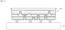
- the light emitting device 100 is bonded onto a circuit board 101 (see FIG. 14 ), and the third substrate 41 may be separated to from the light emitting device 100.
- a schematic cross-sectional view of the light emitting device 100 bonded to the circuit board 101 is exemplarily shown in FIG. 14 .
- FIG. 14 exemplarily illustrates a single light emitting device 100 disposed on the circuit board 101, however, a plurality of light emitting devices 100 may be mounted on the circuit board 101.
- Each of the light emitting devices 100 may form one pixel capable of emitting any one of blue light, green light, and red light, and a plurality of pixels are arranged on the circuit board 101 to provide a display panel.
- the plurality of light emitting devices 100 may be formed on the substrate 41, and the light emitting devices 100 may be transferred onto the circuit board 101 in a group, not individually.
- FIG. 15A, FIG. 15B, and FIG. 15C are schematic cross-sectional views illustrating a method of transferring the light emitting device to the circuit board according to an exemplary embodiment. Hereinafter, a method of transferring the light emitting devices 100 formed on the substrate 41 to the circuit board 101 in a group will be described.
- the plurality of light emitting devices 100 are isolated from each other, and are arranged on the substrate 41 by the isolation trench.
- the circuit board 101 having pads on an upper surface thereof is provided.
- the pads are arranged on the circuit board 101 to correspond to locations where the pixels for a display are to be arranged.
- an interval between the light emitting devices 100 arranged on the substrate 41 may be more dense than that of the pixels on the circuit board 101.
- bump pads of the light emitting devices 100 are selectively bonded to the pads on the circuit board 101.
- the bump pads and the pads may be bonded using In bonding, for example.
- the light emitting devices 100 located between pixel regions may be spaced apart from the circuit board 101, since these light emitting devices 100 do not have pads of the circuit board 101 to be boned to.
- a mask 201 is disposed on the substrate 41 and is irradiated with a laser.
- a light transmitting region of the mask 201 is disposed to correspond to the light emitting devices 100 bonded to the circuit board 101, and thus, the light emitting devices 100 bonded to the pads of the circuit board 101 are selectively irradiated with the laser.
- the light emitting devices 100 are transferred to the circuit board 101 by separating the light emitting devices 100 irradiated with the laser from the substrate 41.
- the display panel in which the light emitting devices 100 are arranged on the circuit board 101 is provided.
- the display panel may be mounted on various display apparatuses as described with reference to FIG. 1 .
- the invention provides, in particular, the following:
Landscapes
- Physics & Mathematics (AREA)
- General Physics & Mathematics (AREA)
- Engineering & Computer Science (AREA)
- Theoretical Computer Science (AREA)
- Led Devices (AREA)
- Led Device Packages (AREA)
- Devices For Indicating Variable Information By Combining Individual Elements (AREA)
Applications Claiming Priority (4)
| Application Number | Priority Date | Filing Date | Title |
|---|---|---|---|
| US201962802784P | 2019-02-08 | 2019-02-08 | |
| US16/782,594 US11362073B2 (en) | 2019-02-08 | 2020-02-05 | Light emitting device including multiple transparent electrodes for display and display apparatus having the same |
| EP20753265.6A EP3923326B1 (de) | 2019-02-08 | 2020-02-06 | Lichtemittierendes element für eine anzeige |
| PCT/KR2020/001703 WO2020162687A1 (ko) | 2019-02-08 | 2020-02-06 | 디스플레이용 발광 소자 및 그것을 가지는 디스플레이 장치 |
Related Parent Applications (1)
| Application Number | Title | Priority Date | Filing Date |
|---|---|---|---|
| EP20753265.6A Division EP3923326B1 (de) | 2019-02-08 | 2020-02-06 | Lichtemittierendes element für eine anzeige |
Publications (2)
| Publication Number | Publication Date |
|---|---|
| EP4407697A2 true EP4407697A2 (de) | 2024-07-31 |
| EP4407697A3 EP4407697A3 (de) | 2024-11-06 |
Family
ID=71945317
Family Applications (2)
| Application Number | Title | Priority Date | Filing Date |
|---|---|---|---|
| EP24169073.4A Pending EP4407697A3 (de) | 2019-02-08 | 2020-02-06 | Lichtemittierendes element für eine anzeige |
| EP20753265.6A Active EP3923326B1 (de) | 2019-02-08 | 2020-02-06 | Lichtemittierendes element für eine anzeige |
Family Applications After (1)
| Application Number | Title | Priority Date | Filing Date |
|---|---|---|---|
| EP20753265.6A Active EP3923326B1 (de) | 2019-02-08 | 2020-02-06 | Lichtemittierendes element für eine anzeige |
Country Status (8)
| Country | Link |
|---|---|
| US (4) | US11362073B2 (de) |
| EP (2) | EP4407697A3 (de) |
| JP (1) | JP7542544B2 (de) |
| KR (1) | KR102752397B1 (de) |
| CN (2) | CN118335864A (de) |
| BR (1) | BR112021014915A2 (de) |
| MX (1) | MX2021009292A (de) |
| WO (1) | WO2020162687A1 (de) |
Families Citing this family (11)
| Publication number | Priority date | Publication date | Assignee | Title |
|---|---|---|---|---|
| US11362073B2 (en) * | 2019-02-08 | 2022-06-14 | Seoul Viosys Co., Ltd. | Light emitting device including multiple transparent electrodes for display and display apparatus having the same |
| US11211528B2 (en) * | 2019-03-13 | 2021-12-28 | Seoul Viosys Co., Ltd. | Light emitting device for display and display apparatus having the same |
| US11437353B2 (en) * | 2019-11-15 | 2022-09-06 | Seoul Viosys Co., Ltd. | Light emitting device for display and display apparatus having the same |
| EP4060753A4 (de) * | 2019-11-15 | 2024-01-17 | Seoul Viosys Co., Ltd | Lichtemittierende vorrichtung für eine anzeige und anzeigevorrichtung damit |
| CN214672619U (zh) * | 2020-05-28 | 2021-11-09 | 首尔伟傲世有限公司 | 发光元件及具有该发光元件的显示装置 |
| US12040344B2 (en) * | 2020-05-28 | 2024-07-16 | Seoul Viosys Co., Ltd. | Light emitting device and display apparatus having the same |
| JP7736073B2 (ja) * | 2021-09-03 | 2025-09-09 | ソニーグループ株式会社 | 発光デバイスおよび電子機器 |
| TWI777853B (zh) * | 2021-11-17 | 2022-09-11 | 隆達電子股份有限公司 | 封裝結構及其形成方法 |
| JP7806539B2 (ja) * | 2022-02-16 | 2026-01-27 | 沖電気工業株式会社 | 発光装置 |
| CN115394762B (zh) * | 2022-05-17 | 2024-07-09 | 诺视科技(苏州)有限公司 | 一种具有透明衬底的像素级分立器件及其制作方法 |
| KR102668393B1 (ko) * | 2022-08-10 | 2024-05-24 | 엘지전자 주식회사 | 디스플레이 화소용 반도체 발광소자 패키지 및 이를 포함하는 디스플레이 장치 |
Family Cites Families (20)
| Publication number | Priority date | Publication date | Assignee | Title |
|---|---|---|---|---|
| US8058663B2 (en) | 2007-09-26 | 2011-11-15 | Iii-N Technology, Inc. | Micro-emitter array based full-color micro-display |
| KR101354981B1 (ko) | 2007-11-14 | 2014-01-27 | 삼성전자주식회사 | 질화물 반도체 발광 다이오드 |
| KR101382836B1 (ko) * | 2007-11-23 | 2014-04-08 | 엘지이노텍 주식회사 | 반도체 발광소자 및 그 제조방법 |
| US7732803B2 (en) * | 2008-05-01 | 2010-06-08 | Bridgelux, Inc. | Light emitting device having stacked multiple LEDS |
| WO2011083923A2 (en) * | 2010-01-07 | 2011-07-14 | Seoul Opto Device Co., Ltd. | Light emitting diode having electrode pads |
| KR101625122B1 (ko) | 2010-01-18 | 2016-05-27 | 서울바이오시스 주식회사 | 전극패드들을 갖는 발광 다이오드 |
| KR101786082B1 (ko) | 2011-01-27 | 2017-10-16 | 엘지이노텍 주식회사 | 발광 소자 |
| KR101293647B1 (ko) * | 2012-07-27 | 2013-08-13 | 삼성코닝정밀소재 주식회사 | 투명 전도성 산화물 박막 기판, 그 제조방법, 이를 포함하는 유기전계발광소자 및 광전지 |
| CN110600593B (zh) * | 2012-12-06 | 2023-01-03 | 首尔伟傲世有限公司 | 发光二极管 |
| JP2015012244A (ja) | 2013-07-01 | 2015-01-19 | 株式会社東芝 | 半導体発光素子 |
| JP6713720B2 (ja) * | 2013-08-30 | 2020-06-24 | エルジー イノテック カンパニー リミテッド | 発光素子パッケージ及びそれを含む車両用照明装置 |
| KR102513080B1 (ko) | 2016-04-04 | 2023-03-24 | 삼성전자주식회사 | Led 광원 모듈 및 디스플레이 장치 |
| KR20180084652A (ko) * | 2017-01-16 | 2018-07-25 | 서울바이오시스 주식회사 | 수직형 발광 다이오드 |
| TWI778010B (zh) | 2017-01-26 | 2022-09-21 | 晶元光電股份有限公司 | 發光元件 |
| KR102430500B1 (ko) * | 2017-05-30 | 2022-08-08 | 삼성전자주식회사 | 반도체 발광소자 및 이를 이용한 led 모듈 |
| KR20190001050A (ko) | 2017-06-26 | 2019-01-04 | 주식회사 루멘스 | 칩 적층 구조를 갖는 led 픽셀 소자 |
| KR102503578B1 (ko) | 2017-06-30 | 2023-02-24 | 엘지전자 주식회사 | 반도체 발광 소자를 이용한 디스플레이 장치 |
| US10643980B2 (en) * | 2018-01-23 | 2020-05-05 | Epistar Corporation | Light-emitting device, manufacturing method thereof and display module using the same |
| CN109192821A (zh) * | 2018-08-31 | 2019-01-11 | 华灿光电(浙江)有限公司 | 发光二极管芯片的转移方法、转移基板及发光二极管阵列 |
| US11362073B2 (en) | 2019-02-08 | 2022-06-14 | Seoul Viosys Co., Ltd. | Light emitting device including multiple transparent electrodes for display and display apparatus having the same |
-
2020
- 2020-02-05 US US16/782,594 patent/US11362073B2/en active Active
- 2020-02-06 KR KR1020217020417A patent/KR102752397B1/ko active Active
- 2020-02-06 MX MX2021009292A patent/MX2021009292A/es unknown
- 2020-02-06 JP JP2021545853A patent/JP7542544B2/ja active Active
- 2020-02-06 EP EP24169073.4A patent/EP4407697A3/de active Pending
- 2020-02-06 EP EP20753265.6A patent/EP3923326B1/de active Active
- 2020-02-06 CN CN202410415848.4A patent/CN118335864A/zh active Pending
- 2020-02-06 BR BR112021014915-5A patent/BR112021014915A2/pt not_active Application Discontinuation
- 2020-02-06 WO PCT/KR2020/001703 patent/WO2020162687A1/ko not_active Ceased
- 2020-02-06 CN CN202080013013.6A patent/CN113424314B/zh active Active
-
2022
- 2022-05-26 US US17/826,106 patent/US12334483B2/en active Active
- 2022-07-31 US US17/878,024 patent/US12355016B2/en active Active
-
2025
- 2025-05-23 US US19/216,971 patent/US20250286028A1/en active Pending
Also Published As
| Publication number | Publication date |
|---|---|
| EP3923326C0 (de) | 2024-04-10 |
| KR102752397B1 (ko) | 2025-01-14 |
| US12355016B2 (en) | 2025-07-08 |
| CN113424314B (zh) | 2024-04-26 |
| US20250286028A1 (en) | 2025-09-11 |
| US20200258872A1 (en) | 2020-08-13 |
| EP4407697A3 (de) | 2024-11-06 |
| US12334483B2 (en) | 2025-06-17 |
| US11362073B2 (en) | 2022-06-14 |
| US20220285329A1 (en) | 2022-09-08 |
| EP3923326A1 (de) | 2021-12-15 |
| US20220367429A1 (en) | 2022-11-17 |
| MX2021009292A (es) | 2021-10-13 |
| EP3923326B1 (de) | 2024-04-10 |
| WO2020162687A1 (ko) | 2020-08-13 |
| JP2022519656A (ja) | 2022-03-24 |
| JP7542544B2 (ja) | 2024-08-30 |
| CN113424314A (zh) | 2021-09-21 |
| EP3923326A4 (de) | 2022-11-02 |
| BR112021014915A2 (pt) | 2021-09-28 |
| CN118335864A (zh) | 2024-07-12 |
| KR20210113983A (ko) | 2021-09-17 |
Similar Documents
| Publication | Publication Date | Title |
|---|---|---|
| EP3923326B1 (de) | Lichtemittierendes element für eine anzeige | |
| US12132148B2 (en) | Light emitting device for display and display apparatus having the same | |
| US12464882B2 (en) | Light emitting device for display and display apparatus having the same | |
| US12154934B2 (en) | Light emitting device for display and display apparatus having the same | |
| US12622331B2 (en) | Light emitting device for display and display apparatus having the same | |
| EP3975270A1 (de) | Lichtemittierendes element für eine anzeige und anzeigevorrichtung damit | |
| CN211088273U (zh) | 显示器用发光元件以及具有该发光元件的显示装置 | |
| US11437353B2 (en) | Light emitting device for display and display apparatus having the same |
Legal Events
| Date | Code | Title | Description |
|---|---|---|---|
| PUAI | Public reference made under article 153(3) epc to a published international application that has entered the european phase |
Free format text: ORIGINAL CODE: 0009012 |
|
| STAA | Information on the status of an ep patent application or granted ep patent |
Free format text: STATUS: REQUEST FOR EXAMINATION WAS MADE |
|
| 17P | Request for examination filed |
Effective date: 20240408 |
|
| AC | Divisional application: reference to earlier application |
Ref document number: 3923326 Country of ref document: EP Kind code of ref document: P |
|
| AK | Designated contracting states |
Kind code of ref document: A2 Designated state(s): AL AT BE BG CH CY CZ DE DK EE ES FI FR GB GR HR HU IE IS IT LI LT LU LV MC MK MT NL NO PL PT RO RS SE SI SK SM TR |
|
| REG | Reference to a national code |
Ref country code: DE Ref legal event code: R079 Free format text: PREVIOUS MAIN CLASS: H01L0033000000 Ipc: H01L0025075000 |
|
| PUAL | Search report despatched |
Free format text: ORIGINAL CODE: 0009013 |
|
| AK | Designated contracting states |
Kind code of ref document: A3 Designated state(s): AL AT BE BG CH CY CZ DE DK EE ES FI FR GB GR HR HU IE IS IT LI LT LU LV MC MK MT NL NO PL PT RO RS SE SI SK SM TR |
|
| RIC1 | Information provided on ipc code assigned before grant |
Ipc: H01L 33/00 20100101ALI20240927BHEP Ipc: H01L 33/20 20100101ALI20240927BHEP Ipc: H01L 33/62 20100101ALI20240927BHEP Ipc: H01L 33/38 20100101ALI20240927BHEP Ipc: H01L 33/42 20100101ALI20240927BHEP Ipc: H01L 25/075 20060101AFI20240927BHEP |