EP4407657A1 - Nitridhalbleitersubstrat und verfahren zur herstellung davon - Google Patents
Nitridhalbleitersubstrat und verfahren zur herstellung davon Download PDFInfo
- Publication number
- EP4407657A1 EP4407657A1 EP22872620.4A EP22872620A EP4407657A1 EP 4407657 A1 EP4407657 A1 EP 4407657A1 EP 22872620 A EP22872620 A EP 22872620A EP 4407657 A1 EP4407657 A1 EP 4407657A1
- Authority
- EP
- European Patent Office
- Prior art keywords
- layer
- nitride semiconductor
- adhesive layer
- substrate
- laminated
- Prior art date
- Legal status (The legal status is an assumption and is not a legal conclusion. Google has not performed a legal analysis and makes no representation as to the accuracy of the status listed.)
- Pending
Links
Images

Classifications
-
- C—CHEMISTRY; METALLURGY
- C30—CRYSTAL GROWTH
- C30B—SINGLE-CRYSTAL GROWTH; UNIDIRECTIONAL SOLIDIFICATION OF EUTECTIC MATERIAL OR UNIDIRECTIONAL DEMIXING OF EUTECTOID MATERIAL; REFINING BY ZONE-MELTING OF MATERIAL; PRODUCTION OF A HOMOGENEOUS POLYCRYSTALLINE MATERIAL WITH DEFINED STRUCTURE; SINGLE CRYSTALS OR HOMOGENEOUS POLYCRYSTALLINE MATERIAL WITH DEFINED STRUCTURE; AFTER-TREATMENT OF SINGLE CRYSTALS OR A HOMOGENEOUS POLYCRYSTALLINE MATERIAL WITH DEFINED STRUCTURE; APPARATUS THEREFOR
- C30B29/00—Single crystals or homogeneous polycrystalline material with defined structure characterised by the material or by their shape
- C30B29/10—Inorganic compounds or compositions
- C30B29/38—Nitrides
-
- H—ELECTRICITY
- H01—ELECTRIC ELEMENTS
- H01L—SEMICONDUCTOR DEVICES NOT COVERED BY CLASS H10
- H01L21/00—Processes or apparatus adapted for the manufacture or treatment of semiconductor or solid state devices or of parts thereof
- H01L21/02—Manufacture or treatment of semiconductor devices or of parts thereof
- H01L21/02104—Forming layers
- H01L21/02365—Forming inorganic semiconducting materials on a substrate
- H01L21/02518—Deposited layers
- H01L21/02521—Materials
- H01L21/02538—Group 13/15 materials
- H01L21/0254—Nitrides
-
- C—CHEMISTRY; METALLURGY
- C30—CRYSTAL GROWTH
- C30B—SINGLE-CRYSTAL GROWTH; UNIDIRECTIONAL SOLIDIFICATION OF EUTECTIC MATERIAL OR UNIDIRECTIONAL DEMIXING OF EUTECTOID MATERIAL; REFINING BY ZONE-MELTING OF MATERIAL; PRODUCTION OF A HOMOGENEOUS POLYCRYSTALLINE MATERIAL WITH DEFINED STRUCTURE; SINGLE CRYSTALS OR HOMOGENEOUS POLYCRYSTALLINE MATERIAL WITH DEFINED STRUCTURE; AFTER-TREATMENT OF SINGLE CRYSTALS OR A HOMOGENEOUS POLYCRYSTALLINE MATERIAL WITH DEFINED STRUCTURE; APPARATUS THEREFOR
- C30B25/00—Single-crystal growth by chemical reaction of reactive gases, e.g. chemical vapour-deposition growth
- C30B25/02—Epitaxial-layer growth
- C30B25/18—Epitaxial-layer growth characterised by the substrate
-
- C—CHEMISTRY; METALLURGY
- C30—CRYSTAL GROWTH
- C30B—SINGLE-CRYSTAL GROWTH; UNIDIRECTIONAL SOLIDIFICATION OF EUTECTIC MATERIAL OR UNIDIRECTIONAL DEMIXING OF EUTECTOID MATERIAL; REFINING BY ZONE-MELTING OF MATERIAL; PRODUCTION OF A HOMOGENEOUS POLYCRYSTALLINE MATERIAL WITH DEFINED STRUCTURE; SINGLE CRYSTALS OR HOMOGENEOUS POLYCRYSTALLINE MATERIAL WITH DEFINED STRUCTURE; AFTER-TREATMENT OF SINGLE CRYSTALS OR A HOMOGENEOUS POLYCRYSTALLINE MATERIAL WITH DEFINED STRUCTURE; APPARATUS THEREFOR
- C30B29/00—Single crystals or homogeneous polycrystalline material with defined structure characterised by the material or by their shape
- C30B29/10—Inorganic compounds or compositions
- C30B29/40—AIIIBV compounds wherein A is B, Al, Ga, In or Tl and B is N, P, As, Sb or Bi
- C30B29/403—AIII-nitrides
- C30B29/406—Gallium nitride
-
- H—ELECTRICITY
- H01—ELECTRIC ELEMENTS
- H01L—SEMICONDUCTOR DEVICES NOT COVERED BY CLASS H10
- H01L21/00—Processes or apparatus adapted for the manufacture or treatment of semiconductor or solid state devices or of parts thereof
- H01L21/02—Manufacture or treatment of semiconductor devices or of parts thereof
- H01L21/02104—Forming layers
- H01L21/02365—Forming inorganic semiconducting materials on a substrate
- H01L21/02367—Substrates
- H01L21/0237—Materials
- H01L21/02373—Group 14 semiconducting materials
- H01L21/02381—Silicon, silicon germanium, germanium
-
- H—ELECTRICITY
- H01—ELECTRIC ELEMENTS
- H01L—SEMICONDUCTOR DEVICES NOT COVERED BY CLASS H10
- H01L21/00—Processes or apparatus adapted for the manufacture or treatment of semiconductor or solid state devices or of parts thereof
- H01L21/02—Manufacture or treatment of semiconductor devices or of parts thereof
- H01L21/02104—Forming layers
- H01L21/02365—Forming inorganic semiconducting materials on a substrate
- H01L21/02436—Intermediate layers between substrates and deposited layers
- H01L21/02439—Materials
- H01L21/02441—Group 14 semiconducting materials
- H01L21/0245—Silicon, silicon germanium, germanium
-
- H—ELECTRICITY
- H01—ELECTRIC ELEMENTS
- H01L—SEMICONDUCTOR DEVICES NOT COVERED BY CLASS H10
- H01L21/00—Processes or apparatus adapted for the manufacture or treatment of semiconductor or solid state devices or of parts thereof
- H01L21/02—Manufacture or treatment of semiconductor devices or of parts thereof
- H01L21/02104—Forming layers
- H01L21/02365—Forming inorganic semiconducting materials on a substrate
- H01L21/02436—Intermediate layers between substrates and deposited layers
- H01L21/02439—Materials
- H01L21/02455—Group 13/15 materials
- H01L21/02458—Nitrides
-
- H—ELECTRICITY
- H01—ELECTRIC ELEMENTS
- H01L—SEMICONDUCTOR DEVICES NOT COVERED BY CLASS H10
- H01L21/00—Processes or apparatus adapted for the manufacture or treatment of semiconductor or solid state devices or of parts thereof
- H01L21/02—Manufacture or treatment of semiconductor devices or of parts thereof
- H01L21/02104—Forming layers
- H01L21/02365—Forming inorganic semiconducting materials on a substrate
- H01L21/02436—Intermediate layers between substrates and deposited layers
- H01L21/02439—Materials
- H01L21/02488—Insulating materials
-
- H—ELECTRICITY
- H01—ELECTRIC ELEMENTS
- H01L—SEMICONDUCTOR DEVICES NOT COVERED BY CLASS H10
- H01L21/00—Processes or apparatus adapted for the manufacture or treatment of semiconductor or solid state devices or of parts thereof
- H01L21/02—Manufacture or treatment of semiconductor devices or of parts thereof
- H01L21/02104—Forming layers
- H01L21/02365—Forming inorganic semiconducting materials on a substrate
- H01L21/02436—Intermediate layers between substrates and deposited layers
- H01L21/02439—Materials
- H01L21/02491—Conductive materials
-
- H—ELECTRICITY
- H01—ELECTRIC ELEMENTS
- H01L—SEMICONDUCTOR DEVICES NOT COVERED BY CLASS H10
- H01L21/00—Processes or apparatus adapted for the manufacture or treatment of semiconductor or solid state devices or of parts thereof
- H01L21/02—Manufacture or treatment of semiconductor devices or of parts thereof
- H01L21/02104—Forming layers
- H01L21/02365—Forming inorganic semiconducting materials on a substrate
- H01L21/02436—Intermediate layers between substrates and deposited layers
- H01L21/02494—Structure
- H01L21/02496—Layer structure
- H01L21/02505—Layer structure consisting of more than two layers
-
- H—ELECTRICITY
- H01—ELECTRIC ELEMENTS
- H01L—SEMICONDUCTOR DEVICES NOT COVERED BY CLASS H10
- H01L21/00—Processes or apparatus adapted for the manufacture or treatment of semiconductor or solid state devices or of parts thereof
- H01L21/02—Manufacture or treatment of semiconductor devices or of parts thereof
- H01L21/02104—Forming layers
- H01L21/02365—Forming inorganic semiconducting materials on a substrate
- H01L21/02518—Deposited layers
- H01L21/0257—Doping during depositing
- H01L21/02573—Conductivity type
- H01L21/02581—Transition metal or rare earth elements
-
- H—ELECTRICITY
- H01—ELECTRIC ELEMENTS
- H01L—SEMICONDUCTOR DEVICES NOT COVERED BY CLASS H10
- H01L21/00—Processes or apparatus adapted for the manufacture or treatment of semiconductor or solid state devices or of parts thereof
- H01L21/02—Manufacture or treatment of semiconductor devices or of parts thereof
- H01L21/02104—Forming layers
- H01L21/02365—Forming inorganic semiconducting materials on a substrate
- H01L21/02612—Formation types
- H01L21/02617—Deposition types
- H01L21/0262—Reduction or decomposition of gaseous compounds, e.g. CVD
-
- H—ELECTRICITY
- H01—ELECTRIC ELEMENTS
- H01L—SEMICONDUCTOR DEVICES NOT COVERED BY CLASS H10
- H01L21/00—Processes or apparatus adapted for the manufacture or treatment of semiconductor or solid state devices or of parts thereof
- H01L21/02—Manufacture or treatment of semiconductor devices or of parts thereof
- H01L21/02104—Forming layers
- H01L21/02365—Forming inorganic semiconducting materials on a substrate
- H01L21/02656—Special treatments
- H01L21/02658—Pretreatments
-
- H—ELECTRICITY
- H10—SEMICONDUCTOR DEVICES; ELECTRIC SOLID-STATE DEVICES NOT OTHERWISE PROVIDED FOR
- H10D—INORGANIC ELECTRIC SEMICONDUCTOR DEVICES
- H10D62/00—Semiconductor bodies, or regions thereof, of devices having potential barriers
- H10D62/80—Semiconductor bodies, or regions thereof, of devices having potential barriers characterised by the materials
- H10D62/82—Heterojunctions
- H10D62/824—Heterojunctions comprising only Group III-V materials heterojunctions, e.g. GaN/AlGaN heterojunctions
-
- H—ELECTRICITY
- H10—SEMICONDUCTOR DEVICES; ELECTRIC SOLID-STATE DEVICES NOT OTHERWISE PROVIDED FOR
- H10D—INORGANIC ELECTRIC SEMICONDUCTOR DEVICES
- H10D62/00—Semiconductor bodies, or regions thereof, of devices having potential barriers
- H10D62/80—Semiconductor bodies, or regions thereof, of devices having potential barriers characterised by the materials
- H10D62/85—Semiconductor bodies, or regions thereof, of devices having potential barriers characterised by the materials being Group III-V materials, e.g. GaAs
- H10D62/8503—Nitride Group III-V materials, e.g. AlN or GaN
Definitions
- the present invention relates to a nitride semiconductor substrate and a method for manufacturing the substrate.
- MOCVD one of the methods for producing a semiconductor thin film, is widely used because of its superiority in diameter enlargement, mass productivity, and ability to form a homogeneous thin film crystal.
- a nitride semiconductor represented by GaN is expected to be a semiconductor material for the next generation, exceeding the limitation of Si as the material.
- GaN has characteristics of high saturated electron velocity and thus can produce a device capable of high-frequency operation and operable at a higher output due to a large dielectric breakdown electric field. Moreover, weight reduction, miniaturization, and lower electric power consumption can be expected. In recent years, the demand for an accelerated communication speed represented by such as 5G and an accompanying higher output has attracted attention toward a GaN HEMT operable at high frequency and high output.
- a Si substrate is the most inexpensive substrate used for a GaN epitaxial wafer to produce a GaN device and is also advantageous for the enlargement of diameter.
- a large-diameter substrate for GaN epitaxial growth (hereinafter, a support substrate for GaN) with a large diameter and a thermal expansion coefficient close to that of GaN is also disclosed in such as Patent Document 1.
- This support substrate for GaN is configured with a support structure including a polycrystalline ceramic core, a first adhesive layer, a conductive layer, a second adhesive layer, and a barrier layer; a planarization layer laminated to one surface of the support structure; and a single crystal silicon layer laminated to the planarization layer.
- a GaN epitaxial substrate with a large diameter, a thick epitaxial layer, and crack-free can be manufactured.
- a support substrate for GaN has an extremely small difference in thermal expansion coefficient from GaN, thus, a warp is less likely to occur during growing and cooling GaN. Consequently, not only the warp of the substrate after film formation can be controlled to a small degree but also the epitaxial film formation time can be shortened, because complicated stress relaxation layers provided in the epitaxial layer is unnecessary, resulting in significant cost reduction for the epitaxial growth.
- the support substrate for GaN is mostly ceramics; thus, not only the substrate is a very hard substrate and less likely to develop plastic deformation, but also, the substrate does not generate wafer cracks, which has not been solved in large diameter GaN/Si.
- Patent Document 1 JP 2020-505767 A
- An object of the present invention is to provide a nitride semiconductor substrate capable of improving the surface morphology of an AlN layer, thereby suppressing the generation of pits on the surface of a nitride semiconductor epitaxial wafer, and a method for manufacturing the nitride semiconductor substrate.
- the present invention provides a nitride semiconductor substrate comprising:
- the average concentration of Y in the AlN layer is within this range, the surface morphology of the AlN does not deteriorate, and thus, a nitride semiconductor substrate can be made with suppressed pit generation on the surface.
- a thickness of the AlN layer is 50 to 150 nm, and an average concentration of Y (Yttrium) from directly above the growth substrate to 300 nm in a thin film growth direction in the nitride semiconductor thin film is 1E15 atoms/cm 3 or higher and 5E19 atoms/cm 3 or lower.
- the AlN layer in the nitride semiconductor thin film is sufficiently covered by an Yttrium-containing region; thus, the AlN layer with excellent surface morphology can be more reliably formed and suppress the pit generation on the surface of the nitride semiconductor thin film.
- the nitride semiconductor layer preferably comprises one or more of GaN, AlN, and AlGaN.
- such a nitride semiconductor layer can be provided on the AlN layer.
- the growth substrate is a substrate having a single-crystal silicon layer formed on a composite substrate with a plurality of layers laminated together, and the nitride semiconductor thin film is formed on the single-crystal silicon layer.
- a nitride semiconductor epitaxial growth substrate having a large diameter, a thick epitaxial layer, and crack-free can be manufactured.
- a warp is less likely to occur during nitride semiconductor growth and cooling; consequently, the warp of the substrate after film formation can be controlled to a small degree.
- the single-crystal silicon layer preferably has a thickness of 100 to 500 nm.
- the single crystal silicon layer can have such a thickness.
- the composite substrate includes a polycrystalline ceramic core, a first adhesive layer laminated entirely to the polycrystalline ceramic core, a second adhesive layer laminated entirely to the first adhesive layer, and a barrier layer laminated entirely to the second adhesive layer, and the single-crystal silicon layer is formed on a planarization layer laminated to only one surface of the composite substrate.
- the growth substrate is largely made of ceramics. Therefore, not only the substrate itself is very hard and is not susceptible to plastic deformation, and but also wafer crack, which has not been solved with the silicon substrate, does not occur.
- the composite substrate may include a conductive layer laminated entirely to the first adhesive layer, between the first adhesive layer and the second adhesive layer.
- Conductivity can be provided to the composite substrate as needed.
- the composite substrate may include a polycrystalline ceramic core, a first adhesive layer laminated entirely to the polycrystalline ceramic core, a barrier layer laminated entirely to the first adhesive layer, a second adhesive layer laminated to a back surface of the barrier layer, and a conductive layer laminated to a back surface of the second adhesive layer, and the single-crystal silicon layer may be formed on a planarization layer laminated on a front surface of the barrier layer of the composite substrate.
- the nitride semiconductor substrate using such a growth substrate does not form a leakage path due to the conductive layer on the surface side of the growth substrate and can have excellent high-frequency characteristics.
- the composite substrate may include a polycrystalline ceramic core, a first adhesive layer laminated entirely to the polycrystalline ceramic core, a conductive layer laminated to a back surface of the first adhesive layer, a second adhesive layer laminated to a back surface of the conductive layer, a barrier layer laminated to a front surface and a side surface of the first adhesive layer, a side surface of the conductive layer, and a side surface and a back surface of the second adhesive layer, and the single-crystal silicon layer may be formed on a planarization layer laminated on a front surface of the barrier layer of the composite substrate.
- the nitride semiconductor substrate using such a growth substrate also does not form a leakage path due to the conductive layer on the surface side of the growth substrate and can have excellent high-frequency characteristics.
- the conductive layer preferably includes a polysilicon layer.
- the conductive layer preferably has a thickness of 150 to 500 nm.
- the conductive layer can be such a layer.
- the polycrystalline ceramic core preferably contains aluminum nitride.
- first adhesive layer and the second adhesive layer preferably include a tetraethyl orthosilicate (TEOS) layer or a silicon oxide (SiO 2 ) layer, and the barrier layer contains silicon nitride.
- TEOS tetraethyl orthosilicate
- SiO 2 silicon oxide
- first adhesive layer and the second adhesive layer preferably have a thickness of 50 to 200 nm, and the barrier layer has a thickness of 100 to 350 nm.
- the thickness of the first adhesive layer, the second adhesive layer, and the barrier layer can have such a layer thickness.
- the planarization layer preferably contains tetraethyl orthosilicate (TEOS) or silicon oxide (SiO 2 ) and has a thickness of 500 to 3000 nm.
- TEOS tetraethyl orthosilicate
- SiO 2 silicon oxide
- the planarization layer can be such a layer.
- the present invention provides a method for manufacturing a nitride semiconductor substrate having a growth substrate and a nitride semiconductor thin film formed on the growth substrate, the method comprising the steps of:
- Y Yttrium
- the AlN layer preferably has a thickness of 50 to 150 nm and an average concentration of Y (Yttrium) from directly above the growth substrate to 300 nm in a thin film growth direction in the nitride semiconductor thin film is preferably 1E15 atoms/cm 3 or higher and 5E19 atoms/cm 3 or lower.
- the AlN layer is sufficiently coated by a Yttrium-containing region in the nitride semiconductor thin film; thus, the AlN layer having excellent surface morphology can be formed more reliably, and generation of a pit on the surface of the nitride semiconductor thin film can be suppressed.
- the growth substrate is configured with a composite substrate including a polycrystalline ceramic core containing Yttria (Y 2 O 3 ) as a bonding material, a first adhesive layer laminated entirely to the polycrystalline ceramic core, a second adhesive layer laminated entirely to the first adhesive layer, and a barrier layer laminated entirely to the second adhesive layer; a planarization layer laminated to only one surface of the composite substrate; and a single-crystal silicon layer formed on the planarization layer; and the nitride semiconductor thin film is formed on the single-crystal silicon layer, and the average concentration of Y (Yttrium) in the AlN layer is 1E15 atoms/cm 3 or higher and 5E19 atoms/cm 3 or lower by adjusting a thickness of the barrier layer in advance.
- Yttria Y 2 O 3
- Y with a predetermined concentration can be diffused more easily and reliably.
- the composite substrate can include a conductive layer laminated entirely to the first adhesive layer, between the first adhesive layer and the second adhesive layer.
- Conductivity can be provided to the composite substrate as needed.
- the growth substrate may be configured with a composite substrate including a polycrystalline ceramic core containing Yttria (Y 2 O 3 ) as a bonding material, a first adhesive layer laminated entirely to the polycrystalline ceramic core, a barrier layer laminated entirely to the first adhesive layer, a second adhesive layer laminated to a back surface of the barrier layer, and a conductive layer laminated to a back surface of the second adhesive layer; a planarization layer laminated to a front surface of the barrier layer of the composite substrate; and a single-crystal silicon layer formed on the planarization layer; and the nitride semiconductor thin film is formed on the single-crystal silicon layer, and the average concentration of Y (Yttrium) in the AlN layer may be 1E15 atoms/cm 3 or higher and 5E19 atoms/cm 3 or lower by adjusting a thickness of the barrier layer in advance.
- Yttria Y 2 O 3
- Such a method for manufacturing the nitride semiconductor substrate can manufacture the nitride semiconductor substrate with excellent high-frequency characteristics, in which a leakage path due to the conductive layer on the front surface side of the composite substrate is not generated.
- the growth substrate may be configured with a composite substrate including a polycrystalline ceramic core containing Yttria (Y 2 O 3 ) as a bonding material, a first adhesive layer laminated entirely to the polycrystalline ceramic core, a conductive layer laminated to a back surface of the first adhesive layer, a second adhesive layer laminated to a back surface of the conductive layer, and a barrier layer laminated to a front surface and a side surface of the first adhesive layer, a side surface of the conductive layer, and a side surface and a back surface of the second adhesive layer; a planarization layer laminated to a front surface of the barrier layer of the composite substrate; and a single-crystal silicon layer formed on the planarization layer; and the nitride semiconductor thin film is formed on the single-crystal silicon layer, and the average concentration of Y (Yttrium) in the AlN layer may be 1E15 atoms/cm 3 or higher and 5E19 atoms/cm 3 or lower by adjusting a thickness
- Such a method for manufacturing the nitride semiconductor substrate can also manufacture the nitride semiconductor substrate with excellent high-frequency characteristics, in which a leakage path due to the conductive layer on the front surface side of the composite substrate is not generated.
- the present invention can provide a nitride semiconductor substrate capable of improving the surface morphology of an AlN layer, thereby suppressing the generation of pits on the surface of a nitride semiconductor epitaxial wafer, and a method for manufacturing the nitride semiconductor substrate.
- the present inventors have studied an improvement of the surface morphology of the AlN layer to suppress the generation of the pit on the epitaxial wafer surface and found out that Yttrium contained in a predetermined concentration in a nitride semiconductor thin film on a growth substrate improves the surface morphology of the AlN layer and suppresses the generation of the pit. Based on this finding, the present invention has been completed.
- the present invention is a nitride semiconductor substrate including a growth substrate and a nitride semiconductor thin film formed on the growth substrate, in which the nitride semiconductor thin film includes an AlN layer formed on the growth substrate and a nitride semiconductor layer formed on the AlN layer, and an average concentration of Y (Yttrium) in the AlN layer is 1E15 atoms/cm 3 or higher and 5E19 atoms/cm 3 or lower.
- the present invention is a method for manufacturing a nitride semiconductor substrate having a growth substrate and a nitride semiconductor thin film formed on the growth substrate, and the method includes (1) providing the growth substrate containing Y (Yttrium) and (2) epitaxially growing an AlN layer on the growth substrate and then epitaxially growing a nitride semiconductor layer on the AlN layer, thereby forming the nitride semiconductor thin film, in which in the step (2), Y in the growth substrate is diffused so that an average concentration of Y (Yttrium) in the AlN layer is 1E15 atoms/cm 3 or higher and 5E19 atoms/cm 3 or lower.
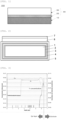
- FIG. 1 shows an example of the inventive nitride semiconductor substrate.
- a nitride semiconductor thin film 40 is formed on a growth substrate 10, and the nitride semiconductor thin film 40 includes an AlN layer 20 formed on the growth substrate 10 and a nitride semiconductor layer 30 formed on the AlN layer 20.
- the inventive nitride semiconductor substrate 100 is characterized by containing a predetermined amount of Yttrium in the AlN layer 20, and an average concentration of Y (Yttrium) in the AlN layer 20 is 1E15 atoms/cm 3 or higher and 5E19 atoms/cm 3 or lower.
- the surface morphology of the AlN layer is improved, and the generation of the pit on an epitaxial layer (nitride semiconductor layer 30) grown on the AlN layer can be suppressed.
- the average concentration of Y in the AlN layer 20 is less than 1E15 atoms/cm 3 , a pit suppression effect is insufficient, and when higher than 5E19 atoms/cm 3 , inherent GaN characteristics are not obtainable.
- a method for measuring the average concentration of Y is not particularly limited but, for example, can be obtained by secondary ion mass spectroscopy (SIMS).
- a thickness of the AlN layer is 50 to 150 nm, and an average concentration of Y (Yttrium) from directly above the growth substrate to 300 nm in a thin film growth direction in the nitride semiconductor thin film is 1E15 atoms/cm 3 or higher and 5E19 atoms/cm 3 or lower.
- Y Yttrium
- the AlN layer in the nitride semiconductor thin film is sufficiently covered by an Yttrium-containing region; thus, the AlN layer with excellent surface morphology can be more reliably formed and suppress the pit generation on the surface of the nitride semiconductor thin film.
- the nitride semiconductor layer formed on the AlN layer preferably comprises one or more of GaN, AlN, and AlGaN.
- a layer in which GaN is laminated on AlGaN or a layer in which a super-lattice structure composed of AlGaN, AlN, and GaN is laminated on AlGaN is more preferable.
- the total thickness of the nitride semiconductor thin film combining the AlN layer and the nitride semiconductor layer is not particularly limited but can be, e.g., 0.5 to 20 um, preferably 1 to 10 ⁇ m.
- the growth substrate is a substrate having a single-crystal silicon layer formed on a composite substrate with a plurality of layers laminated together, and then the nitride semiconductor thin film is formed further on the single-crystal silicon layer.
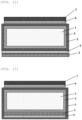
- the support substrate for GaN is, as shown in FIG. 2 for example, configured with a composite substrate (a support structure) including a polycrystalline ceramic core 1, a first adhesive layer 2 laminated entirely to the polycrystalline ceramic core 1, a conductive layer 3 laminated entirely to the first adhesive layer 2, a second adhesive layer 4 laminated entirely to the conductive layer 3, and a barrier layer 5 laminated entirely to the second adhesive layer 4; a planarization layer 6 laminated to only one surface of the composite substrate; and a single-crystal silicon layer 7 laminated to the planarization layer 6.
- a composite substrate a support structure
- a composite substrate including a polycrystalline ceramic core 1, a first adhesive layer 2 laminated entirely to the polycrystalline ceramic core 1, a conductive layer 3 laminated entirely to the first adhesive layer 2, a second adhesive layer 4 laminated entirely to the conductive layer 3, and a barrier layer 5 laminated entirely to the second adhesive layer 4; a planarization layer 6 laminated to only one surface of the composite substrate; and a single-crystal silicon layer 7 laminated to
- the conductive layer 3 and the first adhesive layer 2 are formed as needed, are not always present, and may be formed only on one surface.
- the polycrystalline ceramic core 1 preferably contains aluminum nitride, is sintered using a sintering additive at a high temperature of such as 1800°C, and has a thickness of such as about 600 to 1150 um, and basically, often formed in the thickness of the SEMI standards for Si substrates.
- the first adhesive layer 2 and the second adhesive layer 4 are preferably layers including a tetraethyl orthosilicate (TEOS) layer or a silicon oxide (SiO 2 ) layer, or both layers and are laminated by such as a LPCVD process or a CVD process and have a thickness of about 50 to 200 nm.
- TEOS tetraethyl orthosilicate
- SiO 2 silicon oxide
- the conductive layer 3 preferably includes polysilicon, is laminated by such as the LPCVD process, and has a thickness of about 150 to 500 nm. This is a layer to provides conductivity and is doped with such as boron (B) or phosphorous (P). This conductive layer 3 containing polysilicon is formed as needed and is not always present and may be formed only on one surface.
- the barrier layer 5 preferably contains a silicon nitride layer, is laminated by such as the LPCVD process, and has a thickness of about 100 to 350 nm.
- the planarization layer 6 preferably contains tetraethyl orthosilicate (TEOS) or silicon oxide (SiO 2 ), is laminated by such as the LPCVD process, and has a thickness of about 500 nm to 3000 nm.
- This planarization layer is laminated to planarize the top surface and may be such as typical ceramic film materials, e.g., SiO 2 , Al 2 O 3 , Si 3 N 4 , or silicon oxynitride (Si x O y N z ).
- the single crystal silicon layer 7 preferably has a thickness of about 100 to 500 nm. This is a layer utilized as a growth surface for other epitaxial growth such as GaN and bonded to the planarization layer 6 using such as layer transferring process.
- the thickness, manufacturing methods, materials used, etc. are not limited to the values described above, and not all layers are necessarily present.
- FIG. 12 another example of the support substrate (growth substrate) for GaN, as shown in FIG. 12 , for example, can be configured with a composite substrate including a polycrystalline ceramic core 1, a first adhesive layer 2 bonded entirely to the polycrystalline ceramic core, a barrier layer 5 bonded entirely to the first adhesive layer, a second adhesive layer 4 bonded to a back surface of the barrier layer, and a conductive layer 3 bonded to a back surface of the second adhesive layer; a planarization layer 6 bonded only to a front surface of the composite substrate; and a single-crystal silicon layer 7 bonded to the planarization layer.
- a composite substrate including a polycrystalline ceramic core 1, a first adhesive layer 2 bonded entirely to the polycrystalline ceramic core, a barrier layer 5 bonded entirely to the first adhesive layer, a second adhesive layer 4 bonded to a back surface of the barrier layer, and a conductive layer 3 bonded to a back surface of the second adhesive layer; a planarization layer 6 bonded only to a front surface of the composite substrate;
- Such a nitride semiconductor substrate using the growth substrate with a structure in which the conductive layer 3 is formed only on the back surface side does not generate a leakage path due to the conductive layer on the front surface side of the growth substrate when producing a high-frequency device, resulting in excellent high-frequency characteristics.
- FIG. 13 can be configured with a composite substrate including a polycrystalline ceramic core 1, a first adhesive layer 2 bonded entirely to the polycrystalline ceramic core, a conductive layer 3 bonded to a back surface of the first adhesive layer, a second adhesive layer 4 bonded to a back surface of the conductive layer, and a barrier layer 5 bonded to a front surface and a side surface of the first adhesive layer, a side surface of the conductive layer, and a side surface and a back surface of the second adhesive layer; a planarization layer 6 bonded only to a front surface of the composite substrate; and a single-crystal silicon layer 7 bonded to the planarization layer.
- a composite substrate including a polycrystalline ceramic core 1, a first adhesive layer 2 bonded entirely to the polycrystalline ceramic core, a conductive layer 3 bonded to a back surface of the first adhesive layer, a second adhesive layer 4 bonded to a back surface of the conductive layer, and a barrier layer 5 bonded to a front surface and a side surface of the first adhesive layer
- a nitride semiconductor substrate using the growth substrate with a structure in which the conductive layer 3 is formed only on the back surface side does not generate a leakage path due to the conductive layer on the front surface side of the growth substrate when producing a high-frequency device, resulting in excellent high-frequency characteristics.
- a growth substrate containing Y (Yttrium) is provided (Step (1)), and when a nitride semiconductor thin film is epitaxially grown on the growth substrate, Y in the growth substrate is diffused, thereby making an average concentration of Y (Yttrium) in an AlN layer within a predetermined range (Step (2)).
- the step (1) is a step to provide the growth substrate containing Y (Yttrium).
- the growth substrate containing Y which is a substrate for epitaxial growth, is manufactured.
- the growth substrate is not particularly limited as long as the substrate contains Y; for example, a support substrate for GaN, as described above, can be used.
- yttria Y 2 O 3
- yttria can be used as a bonding material (sintering additive, for example) in the polycrystalline ceramic core in the support substrate for GaN.
- the thickness of the barrier layer (silicon nitride layer) of the support substrate for GaN can be provided in advance, the amount of Yttrium diffused in the epitaxial layer can be controlled with ease in the step (2) as described later, and the average concentration of Y in the AlN layer is more reliably within the predetermined range.
- the thickness of the barrier layer can be, for example, 100 to 350 nm or less.
- the step (2) is a step of epitaxially growing an AlN layer on the growth substrate and then epitaxially growing a nitride semiconductor layer on the AlN layer, thereby forming the nitride semiconductor thin film.
- Y in the growth substrate is diffused so that an average concentration of Y (Yttrium) in the AlN layer is 1E15 atoms/cm 3 or higher and 5E19 atoms/cm 3 or lower.
- the AlN layer e.g., 50 to 150 nm
- an AlGaN layer 100 to 2000 nm
- a group III nitride semiconductor thin film such as GaN is formed on the support substrate for GaN by epitaxial growth.
- TMAl is used as an Al source
- TMGa as a Ga source
- NH 3 as an N source
- the carrier gas is N 2 and H 2 , or either of these gasses, and the process temperature is about 900 to 1200°C.
- the average concentration of Y in the AlN layer is made to be in a range of 1E15 atoms/cm 3 or higher and 5E19 atoms/cm 3 or lower.
- inventive method for manufacturing the nitride semiconductor substrate is not limited to First Aspect described above.
- Y source gas may flow during epitaxial growth of the AlN layer.
- a support substrate for GaN was manufactured as a substrate for epitaxial growth.
- the support substrate for GaN was configured with a composite substrate including a polycrystalline ceramic core (an aluminum nitride core), a first adhesive layer (a silicon oxide layer) laminated entirely to the polycrystalline ceramic core, a conductive layer (a polysilicon layer) laminated entirely to the first adhesive layer, a second adhesive layer (silicon oxide layer) laminated entirely to the conductive layer, and a barrier layer (a silicon nitride layer) laminated entirely to the second adhesive layer; a planarization layer (a silicon oxide layer) laminated only to one surface of the composite substrate; and a single-crystal silicon layer formed on the planarization layer.
- the barrier layer had three levels of thicknesses, i.e., 100 nm, 200 nm, and 350 nm, and yttria (Y 2 O 3 ) was contained as a Y source in the polycrystalline ceramic core.
- group III nitride semiconductor thin films such as AlN, AlGaN, and GaN
- group III nitride semiconductor thin films such as AlN, AlGaN, and GaN
- the support substrate for GaN was mounted on a wafer pocket called a satellite.
- TMAl was used as an Al source
- TMGa as a Ga source
- NH 3 as an N source
- the carrier gas was N 2 and H 2
- the process temperature was 1200°C.
- epitaxial layers were grown from the substrate side to growth direction in the order of AlN and AlGaN, and then GaN was epitaxially grown. Two levels of epitaxial layer structures were produced (Epi-structures 1 and 2).
- a 150 nm AlN layer and a 150 nm AlGaN layer were formed, and then an about 3 um so-called super-lattice structure was formed by repeatedly forming AlGaN, AlN, and GaN in several nm order.
- a GaN layer was formed thereon.
- the total epitaxial layer had a total film thickness of 6.5 ⁇ m.
- AlGaN After forming a 150 nm AlN layer, an about 1.5 um AlGaN was formed so that the Al composition decreased toward the growth direction. A GaN layer was formed on top of that, and the total film thickness of the total epitaxial layer was made to 5.5 ⁇ m.
- Both Epi-structures 1 and 2 were configured to have a device layer on the surface layer side of the epitaxial layer.
- the device layer had a structure having a high crystalline GaN layer (a channel layer) of about 400 nm, in which two-dimensional electron gas was generated, an AlGaN layer (a barrier layer) of about 20 nm for generating two-dimensional electron gas, and on the top layer, a GaN layer (a cap layer) of about 3 nm.
- the barrier layer was made to have an Al composition of 20%.
- the number of pits on the surface was counted by a surface inspection and measurement apparatus and a microscope.
- SIMS analysis Secondary Ion Mass Spectrometry
- Y (Yttrium) concentration in the epitaxial layer was measured.
- SEM Sccanning Electron Microscope
- the barrier layer was made to have a thickness of 500 nm, 800 nm, and 1000 nm. Using these substrates, the same epitaxial growth (2 levels) as in Example and similar evaluations were performed.
- a substrate in which the polycrystalline ceramic core contains no yttria was produced.
- the thickness of the barrier layer was made to 350 nm.
- the same epitaxial growth (2 levels) as in Example and similar evaluations were performed.
- a cross-sectional TEM image of a pit generated was observed.
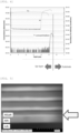
- FIG. 3 and 4 show SIMS measurement results of the nitride semiconductor substrate of Epi-structure 1 in which the barrier layer had a thickness of 100 nm, and the nitride semiconductor substrate of Epi-structure 2 in which the barrier layer had a thickness of 200 nm, both of which were manufactured in Example.
- These nitride semiconductor substrate had a high Y concentration in the epitaxial layer near the interface between the epitaxial layer and the growth substrate, indicating that the average concentration of Y in the AlN layer directly above the growth substrate was within the range of 1E15 atoms/cm 3 or higher and 5E19 atoms/cm 3 or lower.
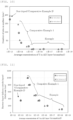
- Other nitride semiconductor substrates manufactured in Example had an average concentration of Y in the AlN layer within the range described above; it was confirmed that the thinner the barrier layer, the higher the average Y concentration ( FIG. 11 ).
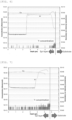
- FIG. 6 and 7 show SIMS measurement results of nitride semiconductor substrates manufactured in Comparative Example 1 having Epi-structure 1 and Epi-structure 2, in which the barrier layer had a thickness of 1000 nm.
- These nitride semiconductor substrates had a Y concentration lower than the detection limit in the epitaxial layer near the interface between the epitaxial layer and the growth substrate, indicating that the average concentration of Y in the AlN layer directly above the growth substrate was less than 1E15 atoms/cm 3 .
- Other nitride semiconductor substrates manufactured in Comparative Examples 1 and 2 also had an average concentration of Y in the AlN layer less than 1E15 atoms/cm 3 ; it was confirmed that the thicker the barrier layer the lower the average concentration of Y ( FIG. 11 ) .
- FIG. 9 shows a TEM image of the pits generated on the surface (In FIG. 9 , the image (b) is an enlarged image of the image (a).).
- each Example had an average concentration of Y in the AlN layer in a range within 1E15 atoms/cm 3 or higher and 5E19 atoms/cm 3 or lower, and thus the generation of pits on a surface was able to be suppressed; however, it was indicated that, when the average concentration of Y in the AlN layer was even a little less than 1E15 atoms/cm 3 as in Comparative Example 1, the generation of pits on the surface was unable to be suppressed.
Landscapes
- Engineering & Computer Science (AREA)
- Chemical & Material Sciences (AREA)
- Computer Hardware Design (AREA)
- Microelectronics & Electronic Packaging (AREA)
- Power Engineering (AREA)
- Condensed Matter Physics & Semiconductors (AREA)
- General Physics & Mathematics (AREA)
- Manufacturing & Machinery (AREA)
- Physics & Mathematics (AREA)
- Crystallography & Structural Chemistry (AREA)
- Materials Engineering (AREA)
- Inorganic Chemistry (AREA)
- Metallurgy (AREA)
- Organic Chemistry (AREA)
- Chemical Kinetics & Catalysis (AREA)
- General Chemical & Material Sciences (AREA)
- Recrystallisation Techniques (AREA)
Applications Claiming Priority (2)
| Application Number | Priority Date | Filing Date | Title |
|---|---|---|---|
| JP2021152843 | 2021-09-21 | ||
| PCT/JP2022/031572 WO2023047864A1 (ja) | 2021-09-21 | 2022-08-22 | 窒化物半導体基板及びその製造方法 |
Publications (2)
| Publication Number | Publication Date |
|---|---|
| EP4407657A1 true EP4407657A1 (de) | 2024-07-31 |
| EP4407657A4 EP4407657A4 (de) | 2025-08-20 |
Family
ID=85720515
Family Applications (1)
| Application Number | Title | Priority Date | Filing Date |
|---|---|---|---|
| EP22872620.4A Pending EP4407657A4 (de) | 2021-09-21 | 2022-08-22 | Nitridhalbleitersubstrat und verfahren zur herstellung davon |
Country Status (6)
| Country | Link |
|---|---|
| US (1) | US20240387170A1 (de) |
| EP (1) | EP4407657A4 (de) |
| JP (1) | JP7652274B2 (de) |
| CN (1) | CN117941030A (de) |
| TW (1) | TW202317822A (de) |
| WO (1) | WO2023047864A1 (de) |
Families Citing this family (1)
| Publication number | Priority date | Publication date | Assignee | Title |
|---|---|---|---|---|
| CN218351409U (zh) * | 2022-06-30 | 2023-01-20 | 苏州晶湛半导体有限公司 | 一种半导体结构 |
Family Cites Families (6)
| Publication number | Priority date | Publication date | Assignee | Title |
|---|---|---|---|---|
| JP4920875B2 (ja) * | 2003-05-29 | 2012-04-18 | パナソニック株式会社 | Iii族窒化物結晶の製造方法、およびiii族窒化物基板の製造方法 |
| WO2012176411A1 (ja) * | 2011-06-24 | 2012-12-27 | 住友化学株式会社 | トランジスタ用半導体基板、トランジスタ及びトランジスタ用半導体基板の製造方法 |
| US9330911B2 (en) * | 2011-08-22 | 2016-05-03 | Invenlux Limited | Light emitting device having group III-nitride current spreading layer doped with transition metal or comprising transition metal nitride |
| KR102188493B1 (ko) * | 2014-04-25 | 2020-12-09 | 삼성전자주식회사 | 질화물 단결정 성장방법 및 질화물 반도체 소자 제조방법 |
| TWI839076B (zh) * | 2016-06-14 | 2024-04-11 | 美商克若密斯股份有限公司 | 用於功率及rf應用的工程基板結構 |
| US10355120B2 (en) | 2017-01-18 | 2019-07-16 | QROMIS, Inc. | Gallium nitride epitaxial structures for power devices |
-
2022
- 2022-08-22 CN CN202280061885.9A patent/CN117941030A/zh active Pending
- 2022-08-22 JP JP2023549420A patent/JP7652274B2/ja active Active
- 2022-08-22 EP EP22872620.4A patent/EP4407657A4/de active Pending
- 2022-08-22 WO PCT/JP2022/031572 patent/WO2023047864A1/ja not_active Ceased
- 2022-08-22 US US18/691,782 patent/US20240387170A1/en active Pending
- 2022-08-26 TW TW111132217A patent/TW202317822A/zh unknown
Also Published As
| Publication number | Publication date |
|---|---|
| EP4407657A4 (de) | 2025-08-20 |
| US20240387170A1 (en) | 2024-11-21 |
| JPWO2023047864A1 (de) | 2023-03-30 |
| WO2023047864A1 (ja) | 2023-03-30 |
| CN117941030A (zh) | 2024-04-26 |
| JP7652274B2 (ja) | 2025-03-27 |
| TW202317822A (zh) | 2023-05-01 |
Similar Documents
| Publication | Publication Date | Title |
|---|---|---|
| US7791106B2 (en) | Gallium nitride material structures including substrates and methods associated with the same | |
| US9748410B2 (en) | N-type aluminum nitride single-crystal substrate and vertical nitride semiconductor device | |
| US10763348B2 (en) | Group III nitride based high electron mobility transistors | |
| US7709360B2 (en) | Method for manufacturing a crystalline silicon layer | |
| US9520286B2 (en) | Semiconductor substrate, semiconductor device and method of manufacturing the semiconductor device | |
| EP4407657A1 (de) | Nitridhalbleitersubstrat und verfahren zur herstellung davon | |
| EP1302976A1 (de) | Einkristalline siliziumscheibe und solarzelle | |
| US7662702B2 (en) | Method for manufacturing a crystalline silicon layer | |
| US11605716B2 (en) | Nitride semiconductor substrate and method of manufacturing the same | |
| EP4442868A1 (de) | Nitridhalbleitersubstrat und verfahren zur herstellung davon | |
| JP7533794B2 (ja) | 窒化物半導体基板の製造方法 | |
| JP7533793B2 (ja) | 窒化物半導体基板及びその製造方法 | |
| EP4354489A1 (de) | Nitridhalbleitersubstrat und verfahren zur herstellung davon | |
| EP4455375A1 (de) | Nitridhalbleitersubstrat und verfahren zur herstellung eines nitridhalbleitersubstrats | |
| JP7207588B1 (ja) | Iii族窒化物半導体ウエーハ及びその製造方法 | |
| CN110189989B (zh) | 硅半导体产品和氮化镓产品的混合生产的方法 | |
| JP2022120821A (ja) | 窒化物半導体基板及びその製造方法 | |
| WO2024228767A1 (en) | Devices comprising a thick (alzga1-z)2o3 layer on a (001) ga2o3 substrate using a (alxga1-x)2o3 buffer layer, and methods of making and use thereof | |
| WO2022177503A1 (en) | Semiconductor apparatus and method for fabricating thereof | |
| CN119843361A (zh) | 一种碳化硅外延结构的制备方法 | |
| JP2020068287A (ja) | 半導体ウエハー及びその製造方法 |
Legal Events
| Date | Code | Title | Description |
|---|---|---|---|
| STAA | Information on the status of an ep patent application or granted ep patent |
Free format text: STATUS: THE INTERNATIONAL PUBLICATION HAS BEEN MADE |
|
| PUAI | Public reference made under article 153(3) epc to a published international application that has entered the european phase |
Free format text: ORIGINAL CODE: 0009012 |
|
| STAA | Information on the status of an ep patent application or granted ep patent |
Free format text: STATUS: REQUEST FOR EXAMINATION WAS MADE |
|
| 17P | Request for examination filed |
Effective date: 20240311 |
|
| AK | Designated contracting states |
Kind code of ref document: A1 Designated state(s): AL AT BE BG CH CY CZ DE DK EE ES FI FR GB GR HR HU IE IS IT LI LT LU LV MC MK MT NL NO PL PT RO RS SE SI SK SM TR |
|
| DAV | Request for validation of the european patent (deleted) | ||
| DAX | Request for extension of the european patent (deleted) | ||
| A4 | Supplementary search report drawn up and despatched |
Effective date: 20250721 |
|
| RIC1 | Information provided on ipc code assigned before grant |
Ipc: H01L 21/20 20060101AFI20250715BHEP Ipc: C30B 25/18 20060101ALI20250715BHEP Ipc: C30B 29/38 20060101ALI20250715BHEP Ipc: H01L 21/205 20060101ALI20250715BHEP Ipc: C30B 29/40 20060101ALI20250715BHEP |