EP4407418A1 - Touch sensing display apparatus - Google Patents
Touch sensing display apparatus Download PDFInfo
- Publication number
- EP4407418A1 EP4407418A1 EP23209603.2A EP23209603A EP4407418A1 EP 4407418 A1 EP4407418 A1 EP 4407418A1 EP 23209603 A EP23209603 A EP 23209603A EP 4407418 A1 EP4407418 A1 EP 4407418A1
- Authority
- EP
- European Patent Office
- Prior art keywords
- touch
- voltage
- gate
- frame
- display
- Prior art date
- Legal status (The legal status is an assumption and is not a legal conclusion. Google has not performed a legal analysis and makes no representation as to the accuracy of the status listed.)
- Granted
Links
Images







Classifications
-
- G—PHYSICS
- G06—COMPUTING OR CALCULATING; COUNTING
- G06F—ELECTRIC DIGITAL DATA PROCESSING
- G06F3/00—Input arrangements for transferring data to be processed into a form capable of being handled by the computer; Output arrangements for transferring data from processing unit to output unit, e.g. interface arrangements
- G06F3/01—Input arrangements or combined input and output arrangements for interaction between user and computer
- G06F3/03—Arrangements for converting the position or the displacement of a member into a coded form
- G06F3/041—Digitisers, e.g. for touch screens or touch pads, characterised by the transducing means
- G06F3/0416—Control or interface arrangements specially adapted for digitisers
- G06F3/04166—Details of scanning methods, e.g. sampling time, grouping of sub areas or time sharing with display driving
-
- G—PHYSICS
- G06—COMPUTING OR CALCULATING; COUNTING
- G06F—ELECTRIC DIGITAL DATA PROCESSING
- G06F3/00—Input arrangements for transferring data to be processed into a form capable of being handled by the computer; Output arrangements for transferring data from processing unit to output unit, e.g. interface arrangements
- G06F3/01—Input arrangements or combined input and output arrangements for interaction between user and computer
- G06F3/03—Arrangements for converting the position or the displacement of a member into a coded form
- G06F3/041—Digitisers, e.g. for touch screens or touch pads, characterised by the transducing means
- G06F3/0412—Digitisers structurally integrated in a display
-
- G—PHYSICS
- G06—COMPUTING OR CALCULATING; COUNTING
- G06F—ELECTRIC DIGITAL DATA PROCESSING
- G06F3/00—Input arrangements for transferring data to be processed into a form capable of being handled by the computer; Output arrangements for transferring data from processing unit to output unit, e.g. interface arrangements
- G06F3/01—Input arrangements or combined input and output arrangements for interaction between user and computer
- G06F3/03—Arrangements for converting the position or the displacement of a member into a coded form
- G06F3/041—Digitisers, e.g. for touch screens or touch pads, characterised by the transducing means
- G06F3/0416—Control or interface arrangements specially adapted for digitisers
- G06F3/04164—Connections between sensors and controllers, e.g. routing lines between electrodes and connection pads
-
- G—PHYSICS
- G06—COMPUTING OR CALCULATING; COUNTING
- G06F—ELECTRIC DIGITAL DATA PROCESSING
- G06F3/00—Input arrangements for transferring data to be processed into a form capable of being handled by the computer; Output arrangements for transferring data from processing unit to output unit, e.g. interface arrangements
- G06F3/01—Input arrangements or combined input and output arrangements for interaction between user and computer
- G06F3/03—Arrangements for converting the position or the displacement of a member into a coded form
- G06F3/041—Digitisers, e.g. for touch screens or touch pads, characterised by the transducing means
- G06F3/044—Digitisers, e.g. for touch screens or touch pads, characterised by the transducing means by capacitive means
-
- G—PHYSICS
- G06—COMPUTING OR CALCULATING; COUNTING
- G06F—ELECTRIC DIGITAL DATA PROCESSING
- G06F3/00—Input arrangements for transferring data to be processed into a form capable of being handled by the computer; Output arrangements for transferring data from processing unit to output unit, e.g. interface arrangements
- G06F3/01—Input arrangements or combined input and output arrangements for interaction between user and computer
- G06F3/03—Arrangements for converting the position or the displacement of a member into a coded form
- G06F3/041—Digitisers, e.g. for touch screens or touch pads, characterised by the transducing means
- G06F3/044—Digitisers, e.g. for touch screens or touch pads, characterised by the transducing means by capacitive means
- G06F3/0446—Digitisers, e.g. for touch screens or touch pads, characterised by the transducing means by capacitive means using a grid-like structure of electrodes in at least two directions, e.g. using row and column electrodes
-
- G—PHYSICS
- G06—COMPUTING OR CALCULATING; COUNTING
- G06F—ELECTRIC DIGITAL DATA PROCESSING
- G06F2203/00—Indexing scheme relating to G06F3/00 - G06F3/048
- G06F2203/041—Indexing scheme relating to G06F3/041 - G06F3/045
- G06F2203/04111—Cross over in capacitive digitiser, i.e. details of structures for connecting electrodes of the sensing pattern where the connections cross each other, e.g. bridge structures comprising an insulating layer, or vias through substrate
-
- G—PHYSICS
- G06—COMPUTING OR CALCULATING; COUNTING
- G06F—ELECTRIC DIGITAL DATA PROCESSING
- G06F2203/00—Indexing scheme relating to G06F3/00 - G06F3/048
- G06F2203/041—Indexing scheme relating to G06F3/041 - G06F3/045
- G06F2203/04112—Electrode mesh in capacitive digitiser: electrode for touch sensing is formed of a mesh of very fine, normally metallic, interconnected lines that are almost invisible to see. This provides a quite large but transparent electrode surface, without need for ITO or similar transparent conductive material
-
- H—ELECTRICITY
- H10—SEMICONDUCTOR DEVICES; ELECTRIC SOLID-STATE DEVICES NOT OTHERWISE PROVIDED FOR
- H10K—ORGANIC ELECTRIC SOLID-STATE DEVICES
- H10K59/00—Integrated devices, or assemblies of multiple devices, comprising at least one organic light-emitting element covered by group H10K50/00
- H10K59/40—OLEDs integrated with touch screens
Definitions
- the present disclosure relates to a touch sensing display apparatus.
- Touch sensors are simple in configuration and small in number of abnormal operations and provide the convenience of users, and thus, are being applied to various display apparatuses.
- Touch sensing display apparatuses may alternately drive a display frame and a touch frame, based on a time division scheme, and thus, may sense a touch input while an image is being displayed on a screen.
- Touch sensing display apparatuses because a conventional gate driving circuit is intactly used for time division driving, a scan output time for touch sensing is insufficient, and due to this, it is difficult to increase touch performance.
- the present disclosure may provide a touch sensing display apparatus which may sufficiently secure a scan output time for touch sensing to enhance touch performance.
- a touch sensing display apparatus includes a display panel where display driving of the display panel to display an image and touch sensing driving of the display panel to sense touch of the display panel are alternately implemented at a predetermined period of time.
- the display panel is configured to be switched between a non-touch driving mode and a touch driving mode, wherein in the non-touch driving mode, the display panel is configured to display an image in all (time) frames, each frame being a display frame, wherein in the touch-driving mode, the display panel is configured to display an image in a display frame and to sense a touch of the display panel in a touch frame, wherein the display frame and the touch frame in the touch-driving mode are alternately performed at predetermined periods of time.
- the touch sensing display apparatus further comprises a gate driving circuit including a plurality of stages whose operations are sequentially activated (meaning configured to be sequentially activated during operations) to drive gate lines of the display panel, wherein each of the plurality of stages is activated in operation according to a display carry clock having a voltage level that changes between a gate on voltage and a gate off voltage in a display frame and output a display scan signal to the display panel during the display driving (displaying of the image), and wherein each of the plurality of stages is activated in operation according to a touch carry clock changing between the gate on voltage and the gate off voltage in a touch frame and output a touch scan signal to the display panel during the touch sensing driving (sensing of the touch), and an on pulse width of the touch carry clock while the touch carry clock is at the gate on voltage is narrower than an on pulse width of the display carry clock while the display carry clock is at the gate on voltage.
- a gate driving circuit including a plurality of stages whose operations are sequentially activated (meaning configured to be sequentially
- An on pulse is referred to a first logic state of a digital signal that is opposite to an off pulse width being a second logic state of the digital signal.
- the sum of on pulse and off pulse may define a time period of the signal.
- An on pulse width is the time duration between two adjacent edges of the on pulse.
- a frame herein is referred to a time frame.
- One frame may include a vertical active period where new image data is scanned or refreshed or updated.
- One Frame may additionally include a vertical blank period where scanning of the image data is not performed.
- the displaying of the image herein also referred to as display driving, that for instance is a not-touch driving mode, may be performed in a vertical active period of a display frame.
- the sensing of the touch herein also referred to as touch sensing driving, that for instance is a touch driving mode, may be performed in a vertical active period of a touch frame.
- An external compensation operation hereinafter also referred to as external compensation driving, may be performed in a vertical blank period of each of the display frame and the touch frame.
- the external compensation driving may be for sensing a device characteristic value (a threshold voltage and electron mobility of a driving transistor and a threshold voltage of a light emitting device) of a pixel.
- all frames may be display frames for display driving (displaying the image that may include external compensation).
- a display frame for display driving and a touch frame for touch sensing driving may be alternately performed (implemented) at a period of a certain time.
- the certain time may be a one-frame time (duration) or it may be a plurality of frame times, e.g. several frames.
- a touch frame is after the display frame.
- one display frame may be arranged between two touch frames.
- a plurality of adjacent display frames may be arranged (on-block) between two touch frames.
- a plurality of adjacent display frames may be arranged (on-block) between adjacent touch frames.
- the non-touch driving mode of the touch sensing display apparatus preferably the display panel of the touch sensing display apparatus may be switched into a touch driving mode of the touch sensing display apparatus, preferably the display panel of the touch sensing display apparatus and vice versa. This switching may be performed based on a signal that is generated from the timing controller.
- the non-touch driving mode may be referred to as display driving mode.
- the touch driving mode may be referred to as display-and-touch driving mode.
- Each of the non-touch driving mode and the touch driving mode may be switched based on whether there is a touch input, and/or a mode selection information about a user, and/or a distance information between a display apparatus and a user.
- the non-touch driving mode e.g. that may also be referred to as display driving mode, may be a driving mode for performing a display operation and an external compensation operation, preferably for displaying of the image.
- the touch driving mode e.g. that may also be referred to as display-and-touch driving mode, may be a driving mode for performing a touch sensing operation in addition to a display operation and an external compensation operation.
- all frames may be display frames for display driving.
- a display frame for display driving and a touch frame for touch sensing driving may be alternately performed at a period of a certain time.
- a touch frame is after the display frame.
- the certain time may be a one-frame time, and in this case, one display frame may be arranged between adjacent touch frames.
- the inventive concept is not limited thereto.
- the certain time may be a several-frame times, and in this case, a plurality of display frames may be arranged between adjacent touch frames.
- An on pulse width of the touch scan signal that turns on pixels of the display panel during the touch frame may be wider than an on pulse width of the display scan signal that turns on the pixels of the display panel during the display frame.
- the display panel may comprise a plurality of touch screen blocks, each may be configured to be individually driven.
- the plurality of stages may comprise a first stage of the plurality stages that is configured to output a first touch scan signal having a first on pulse to a first touch screen block of the display panel during the touch frame based on a first touch scan clock having the gate on voltage, the first touch screen block including a first plurality of rows of pixels.
- the first stage may supply the first touch scan signal to one first gate line included in the first touch screen block without the first touch scan signal being supplied to remaining first gate lines included in the first touch screen block.
- the plurality of stages may comprise a second stage of the plurality stages that may output a second touch scan signal having a second on pulse to a second touch screen block of the display panel during the touch frame based on a second touch scan clock having the gate on voltage, the second touch screen block including a second plurality of rows of pixels.
- a phase of the first touch scan clock may be different from a phase of the second touch scan clock.
- a length of the first on pulse of the first touch scan signal may be equal to a length of the second on pulse of the second touch scan signal.
- the second stage may supply the second touch scan signal to one second gate line included in the second touch screen block without the second touch scan signal being supplied to remaining second gate lines included in the second touch screen block.
- the plurality of stages further comprises one or more third stages arranged between the first stage and the second stage, the one or more third stages configured to supply a third touch scan signal having an off period but no on pulse to one or more third gate lines arranged between the one first gate line and the one second gate line during the touch frame based on a touch scan clock having a gate off voltage.
- a sensing circuit may be configured to sense a voltage of a source node of a representative pixel that is on a substrate of the display panel according to the touch scan signal, the sensed voltage indicative of whether a touch input is applied to the display panel during the touch frame.
- the representative pixel may comprise a storage capacitor and a driving transistor, the driving transistor may include a source electrode connected with the source node and a gate electrode connected with a gate node,
- the gate node may comprise a first conductive pattern that faces the source node with one or more insulation layers between the gate node and the source node and may be a first electrode of the storage capacitor.
- the gate node may comprise a second conductive pattern that is connected with the first conductive pattern through a contact hole passing through the one or more insulation layers.
- the source node may comprise a third conductive pattern on the one or more insulation layers and may be a second electrode of the storage capacitor.
- the first conductive pattern may be closest to the substrate among the first conductive pattern, the second conductive pattern, and the third conductive pattern.
- the second conductive pattern may be on the one or more insulation layers and may comprise a same material as a material of the third conductive pattern.
- a driving current of the representative pixel and the voltage of the source node may change according to the touch input.
- a first driving current of the representative pixel while there is a touch input at a position of the representative pixel may be less than a second driving current of the representative pixel while there is no touch input at the position of the representative pixel.
- a voltage of the source node of the representative pixel while there is a touch input at a position of the representative pixel may be less than a voltage of the source node of the representative pixel while there is no touch input at the position of the representative pixel.
- the gate driving circuit may further include a dummy stage that is disposed at a previous stage that is prior to a first stage of the plurality of stages.
- the gate driving circuit may further include a gate driving voltage line that may be configured to transfer a high-level voltage and a low-level voltage, supplied from a power supply circuit, to the plurality of stages and the dummy stage.
- the high-level voltage and the low-level voltage may each be respectively set to a plurality of different voltage levels.
- the representative pixel may comprise a driving transistor including a source electrode connected with the source node and a gate electrode connected with a gate node.
- the gate node may be closer to the substrate than the source node.
- the representative pixel may include a gate node that is electrically disconnected from the source node.
- a number of the plurality of stages may be a quarter of a number of the gate lines.
- the present embodiments may realize the following effects.
- the number of additional elements for touch sensing may be reduced, and touch sensing performance may be enhanced.
- an on-pulse width of a carry clock may be designed narrower in touch sensing driving than display driving, and thus, a transfer time of a carry signal may be shortened in a touch frame.
- a time capable of being allocated for an output of a touch scan signal in a touch frame may be long secured in proportion to a reduction in transfer time of the carry signal, and thus, touch performance may increase.
- a scan signal (or a gate signal) applied to pixels may swing between a gate on voltage and a gate off voltage.
- the gate on voltage may be set to a voltage which is higher than a threshold voltage of a transistor, and the gate off voltage may be set to a voltage which is lower than the threshold voltage of the transistor.
- the transistor may be turned on in response to the gate on voltage and may be turned off in response to the gate off voltage.
- the gate on voltage may be a gate high voltage (VGH)
- the gate off voltage may be a gate low voltage (VGL).
- the gate on voltage may be the gate low voltage (VGL)
- the gate off voltage may be the gate high voltage (VGH).
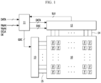
- FIG. 1 is a block diagram illustrating a touch sensing display apparatus according to an embodiment of the present disclosure.
- FIG. 2 is a diagram illustrating a connection configuration of a pixel array and a source driver integrated circuit according to an embodiment of the present disclosure.
- the touch sensing display apparatus may include a display panel 10, a timing controller 11, a data driving circuit 12, a gate driving circuit 13, and a sensing circuit SU.
- the sensing circuit SU may be embedded in the data driving circuit 12, but is not limited thereto.
- first signal lines 14 extending in a column direction may intersect with second signal lines 15 extending in a row direction (or a horizontal direction), and a plurality of pixels P may be respectively provided in a plurality of intersection areas and may be arranged as a matrix type to configure a pixel array.
- the first signal lines 14 may include a plurality of data lines 14A through which data voltages are supplied and a plurality of reference voltage lines 14B through which a reference voltage is supplied.
- the reference voltage lines 14B may connect the pixels P with the sensing circuit SU and may be referred to as a sensing line.
- the second signal lines 15 may be gate lines through which scan signals are supplied.
- the pixel array may include a plurality of pixel set lines PL.
- the pixel set line PL may not denote a physical signal line but may be defined as a pixel set of pixels of one line arranged adjacent to one another in a horizontal direction or defined as a pixel block of pixels of one line.
- the pixels P may be grouped into a plurality of groups and may implement various colors.
- a pixel group for implementing colors is defined as a unit pixel UPXL
- one unit pixel UPXI may include red (R), green (G), blue (B), and white (W) pixels.
- the R, G, B, and W pixels configuring the one-unit pixel UPXI may be arranged adjacent to one another in a horizontal direction and may be designed to share the same reference voltage line 14B, and thus, the pixel array may be simplified.
- the timing controller 11 may be configured to provide a signal that switches (converts) a non-touch driving mode of the touch sensing display apparatus, preferably the display panel of the touch sensing display apparatus into a touch driving mode of the touch sensing display apparatus, preferably the display panel of the touch sensing display apparatus and vice versa.
- the non-touch driving mode may be referred to as display driving mode.
- the touch driving mode may be referred to as display-and-touch driving mode.
- each of the non-touch driving mode and the touch driving mode may be switched based on whether there is a touch input, and/or a mode selection information about a user, and/or a distance information between a display apparatus and a user.
- the non-touch driving mode may be a driving mode for performing a display operation and an external compensation operation, preferably for displaying an image.
- the touch driving mode e.g. that may also be referred to as non-display driving mode, may be a driving mode for further performing a touch sensing operation in addition to a display operation and an external compensation operation.
- all frames may be display frames for display driving.
- a display frame for display driving and a touch frame for touch sensing driving may be alternately performed at a period of a certain time.
- a touch frame is after the display frame.
- the certain time may be a one-frame time, and in this case, one display frame may be arranged between two (adjacent) touch frames.
- the inventive concept is not limited thereto.
- the certain time may be a several-frames (frame times,) and in this case, a plurality of (adjacent) display frames may be arranged (on-block) between two (adjacent) touch frames.
- One frame may include a vertical active period where new image data DATA is scanned (or refreshed or updated) and a vertical blank period where scanning of the image data DATA is not performed.
- Display driving e.g. the displaying of the image in the non-touch driving mode and the touch-driving mode
- touch sensing driving e.g. the sensing of the touch in the touch driving mode
- External compensation driving may be performed in a vertical blank period of each of the display frame and the touch frame.
- the external compensation driving may be for sensing a device characteristic value (a threshold voltage and electron mobility of a driving transistor and a threshold voltage of a light emitting device) of a pixel P.
- the timing controller 11 may correct digital video data input from a host system by using a compensation value based on a pixel sensing value based on external compensation driving, and then, may supply corrected image data DATA to the data driving circuit 12.
- the timing controller 11 may receive a timing signal such as a vertical synchronization signal Vsync, a horizontal synchronization signal Hsync, a data enable signal DE, and a dot clock DCLK from the host system to generate a gate timing control signal GDC for controlling an operation timing of the gate driving circuit 13 and a data timing control signal DDC for controlling an operation timing of the data driving circuit 12.
- the timing controller 11 may compare a predetermined reference value with a touch sensing value based on a touch sensing operation to obtain coordinate information about a touch input position and may transfer the coordinate information to the host system.
- the host system may execute a touch application corresponding to the coordinate information.
- the data driving circuit 12 may include one or more source driving ICs SDIC.
- Each of the source driving Ics SDIC may include a latch array, a plurality of digital-to-analog converters DAC respectively connected to the data lines 14A, a plurality of sensing circuits SU respectively connected to the sensing lines 14B, a plurality of multiplex switches SS which selectively connect the sensing circuits SU to a plurality of analog-to-digital converters ADC, and a shift register SR which sequentially turns on the multiplex switches SS.
- the latch array may latch the corrected image data DATA input from the timing controller 11, based on the data control signal DDC, and may supply the latched image data DATA to the digital-to-analog converters DAC.
- the digital-to-analog converters DAC may convert the latched image data DATA into display data voltages and may supply the display data voltages to the data lines 14A.
- the digital-to-analog converters DAC may generate a predetermined external sensing data voltage and may supply the external sensing data voltage to the data lines 14A.
- touch sensing driving the digital-to-analog converters DAC may generate a predetermined touch driving data voltage and may supply the touch driving data voltage to the data lines 14A.
- the sensing circuit SU may be used in common in external compensation driving and touch sensing driving, and thus, a separate touch sensing circuit for touch sensing may be removed. Because touch sensing is possible without the separate touch sensing circuit, the source driving IC may be simplified, and thus, power consumption and the manufacturing cost may be reduced.
- the sensing circuit SU may supply a reference voltage Vpre to the sensing line 14B, based on the data control signal DDC, or may sample a touch sensing value or a device characteristic sensing value input through the sensing line 14B and may supply a sampled touch sensing value or device characteristic sensing value to the analog-to-digital converter ADC.
- the analog-to-digital converter ADC may receive a clock signal, convert the touch sensing value or the device characteristic sensing value, input from the sensing circuits SU, into a digital sensing signal SLV and may transfer the digital sensing signal SLV to the timing controller 11.
- the gate driving circuit 13 may generate a scan signal (e.g a scan signal SCAN of FIG. 3 ) suitable for display driving, external compensation driving, and touch sensing driving, based on the gate control signal GDC by using a stage circuit STG, and then, may supply the scan signal SCAN to the gate lines 15.
- the scan signal may include a display scan signal for display driving, an external sensing scan signal for external compensation driving, and a touch scan signal for touch sensing driving.
- An on pulse of the display scan signal may correspond to a supply timing of a display data voltage.
- An on pulse of the external sensing scan signal may correspond to a supply timing of an external sensing data voltage.
- An on pulse of the touch scan signal may correspond to a supply timing of a touch driving data voltage.
- the gate control signal GDC may include a plurality of scan clocks and a plurality of carry clocks.
- An on-pulse width of the carry clock e.g. a display carry clock or a touch carry clock, may be designed narrower in touch sensing driving than display driving, and thus, a transfer time of a carry signal may be shortened in a touch frame.
- a time capable of being allocated for an output of a touch scan signal in a touch frame may increase in proportion to a reduction in transfer time of the carry signal, and thus, touch performance may be enhanced.
- FIG. 3 is a diagram illustrating a connection configuration of a pixel P and a sensing circuit SU according to an embodiment of the present disclosure.
- the pixel P may be implemented in a structure capable of an external compensation operation and a touch sensing operation.
- the pixel P may include a light emitting device OLED, a driving transistor DT, a storage capacitor Cst, a first switch transistor ST1, and a second switch transistor ST2.
- the transistors DT, ST1, and ST2 may each be implemented as a thin film transistor (TFT).
- TFTs may be implemented as a P type, an N type, or a hybrid type where the P type and the N type are provided in common.
- a semiconductor layer of a TFT may include amorphous silicon, polysilicon, or oxide.
- the light emitting device OLED may include an anode electrode connected to a source node DTS, a cathode electrode connected to an input terminal of a low-level driving voltage EVSS, and an organic compound layer disposed between the anode electrode and the cathode electrode.
- the organic compound layer may include a hole injection layer (HIL), a hole transport layer (HTL), an emission layer (EML), an electron transport layer (ETL), and an electron injection layer (EIL).
- the driving transistor DT may control a level of a drain-source current (hereinafter referred to as Ids) of the driving transistor DT input to the light emitting device OLED, based on a gate-source voltage (hereinafter referred to as Vgs) thereof.
- the driving transistor DT may include a gate electrode connected with a gate node DTG, a drain electrode connected with an input terminal of a high-level driving voltage EVDD, and a source electrode connected with a source node DTS.
- the storage capacitor Cst may be connected between the gate node DTG and the source node DTS and may hold the gate-source voltage of the driving transistor DT during a predetermined period.
- the first switch transistor ST1 may electrically connect a data line 14A with the gate node DTG, based on a scan signal SCAN from a gate line 15, and may allow a data voltage Vdata to be charged into the gate node DTG.
- the first switch transistor ST1 may include a gate electrode connected with the gate line 15, a drain electrode connected with the data line 14A, and a source electrode connected with the gate node DTG.
- the second switch transistor ST2 may electrically connect the source node DTS with the sensing line 14B, based on the scan signal SCAN, and thus, may allow a reference voltage Vpre to be charged into the source node DTS. Also, the second switch transistor ST2 may allow a source node voltage, corresponding to the Ids of the driving transistor DT, to be charged into a line capacitor LCa of the sensing line 14B.
- the second switch transistor ST2 may include a gate electrode connected with the gate line 15, a drain electrode connected with the sensing line 14B, and a source electrode connected with the source node DTS.
- the sensing circuit SU may be implemented as a voltage sensing type.
- the sensing circuit SU may be for sensing a voltage stored in the line capacitor Lca of the sensing line 14B and may include a reference voltage control switch SW1, a sampling switch SW2, and a sample and hold unit S/H.
- the reference voltage control switch SW1 may be turned on and may connect an input terminal of the reference voltage Vpre with the sensing line 14B, based on the reference control voltage signal SPRE.
- the sampling switch SW2 may be turned on and may connect the sensing line 14B with the sample and hold unit S/H, based on the sampling control signal SAM.
- the Vgs of the driving transistor DT may vary, and thus, the Ids of the driving transistor DT may vary.
- a voltage of the source node DTS of the driving transistor DT may vary based on a level of the Ids of the driving transistor DT. While the second switch transistor ST2 is turned on, the voltage of the source node DTS of the driving transistor DT may be stored in the line capacitor Lca of the sensing line 14B.
- the sample and hold unit S/H may sample and hold the voltage of the source node DTS of the driving transistor DT stored in the line capacitor Lca of the sensing line 14B while the sampling switch SW2 is turned on, and then, may transfer a sampled voltage to the analog-to-digital converter ADC.
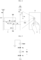
- FIGs. 4 and 5 are diagrams illustrating a concept for sensing a variation of a source node voltage of a pixel based on a touch input (e.g. in a touch driving mode) according to an embodiment of the present disclosure.
- the Vgs of the driving transistor may be reduced by a touch capacitor Ctouch between the touch input object and the driving transistor.
- the touch capacitor Ctouch may be a capacitive capacitor between the touch input object and a gate node DTG of the driving transistor.
- the Ids may be proportional to the square of Vgs. Accordingly, even when the amount of Vgs variation based on a touch input is small, the Ids may be amplified, and thus, the source node voltage Vs may be quickly shifted, thereby enhancing touch sensing performance.
- Vg may denote a gate node voltage of the driving transistor.
- FIG. 6 is a diagram illustrating a cross-sectional structure of a circuit unit of a representative pixel P capable of touch sensing according to an embodiment of the present disclosure.
- the touch sensing apparatus may sense a touch input with respect to only some pixels (hereinafter referred to as representative pixels), and thus, a touch sensing period may be shortened, thereby enhancing a touch report rate.
- the representative pixel P may include an emission portion EP which displays an image and a circuit unit CP which does not display an image.
- the emission portion EP of the representative pixel P may include the light emitting device OLED of FIG. 3 .
- the circuit unit CP of the representative pixel P may include the driving transistor DT, the storage capacitor Cst, the first switch transistor ST1, and the second switch transistor ST2 of FIG. 3 .
- the circuit unit CP of the representative pixel P may include insulation layers BUF, GI, and OC and conductive patterns M1, M2, and PXL stacked on a substrate GLS.
- touch sensing performance may increase.
- a gate node connected with the gate electrode of the driving transistor is disposed closer to the substrate GLS than a source node connected with the source electrode of the driving transistor. Therefore, reactivity on a touch input may be improved.
- the source node of the driving transistor is connected with an internal capacitor of the light emitting device, when the source node is disposed closer to the substrate GLS than the gate node, a variation of Vgs (i.e., reactivity on a touch input) corresponding to the touch input may be very small, and thus, may be unsuitable for touch sensing.
- the internal capacitor of the light emitting device may be a capacitor which is between an anode electrode PXL and a cathode electrode.
- a voltage of a source node DTS of the representative pixel P may be a target for touch sensing.
- the representative pixel P may include a gate node DTG which is electrically disconnected from the source node DTS.
- the gate node DTG may include a first conductive pattern M1, which faces the source node DTS with one or more insulation layers GI and BLTF therebetween and is one electrode of the storage capacitor Cst, and a second conductive pattern M2 which is connected with the first conductive pattern M1 through a first contact hole CH1 passing through the insulation layers GI and BUF.
- the source node DTS may be a third conductive pattern M3 which is disposed on the insulation layers GI and BUF and is the other electrode of the storage capacitor Cst.
- the first conductive pattern M1 among the first conductive pattern M1, the second conductive pattern M2, and the third conductive pattern M3 may be disposed closest to the substrate GLS.
- the first conductive pattern M1 formed close to the substrate GLS may function as a touch electrode, and moreover, may function as a light blocking pattern.
- the first conductive pattern M1 may block external light which is incident on a semiconductor layer ACT of the driving transistor, thereby preventing a characteristic value of the driving transistor from being degraded by the external light.
- the first conductive pattern M1 may be covered by a buffer insulation layer BLTF and a gate insulation layer GI and may be electrically connected with the second conductive pattern M2, disposed on the gate insulation layer GI, through the first contact hole CH1.
- the second conductive pattern M2 may configure the gate electrode of the driving transistor.
- the third conductive pattern M3 which is the other electrode of the storage capacitor Cst may be disposed on the first conductive pattern M1 with the buffer insulation layer BUF and the gate insulation layer GI therebetween.
- the third conductive pattern M3 may include the same material as that of the second conductive pattern M2 and may configure the same layer along with the second conductive pattern M2.
- the source electrode of the driving transistor may be formed by providing a conductivity of the semiconductor layer ACT or stacking a conductive layer on the semiconductor layer ACT and may be electrically connected with the third conductive pattern M3 through a contact hole.
- the second conductive pattern M2 and the third conductive pattern M3 may be covered by a planarization layer OC, and the anode electrode PXL of the light emitting device may be formed on the planarization layer OC.
- the source node DTS of the driving transistor and the anode electrode PXL of the light emitting device may be electrically connected with each other through a contact hole passing through the planarization layer OC.
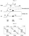
- FIG. 7 is a diagram illustrating a voltage variation of each of a gate node and a source node of a driving transistor, based on whether there is a touch input (e.g. in a touch driving mode) according to an embodiment of the present disclosure.
- a touch input corresponding to representative pixels may be sensed in an on-pulse period ON of a touch scan signal T-SCAN.
- OFF in FIG. 7 refers to an off-pulse period.
- a touch driving data voltage may be applied to a gate node DTG of a driving transistor and a reference voltage Vpre may be applied to a source node DTS of the driving transistor, and thus, the driving transistor may be turned on and Ids may flow in the driving transistor.
- Ids1 corresponding to Vgs1 may flow in the driving transistor.
- the Ids1 of the driving transistor may be less than Ids2 of when there is no touch input.
- Ids1 of a first representative pixel corresponding to a position at which there is a touch input may be less than Ids2 of a second representative pixel corresponding to a position at which there is no touch input.
- a voltage of the source node DTS of the driving transistor may be sensed as Vsen based on Ids1.
- the Vsen of the driving transistor may be less than Vsen' based on Ids2 of when there is no touch input.
- Vsen of the first representative pixel corresponding to a position at which there is a touch input may be less than Vsen' of the second representative pixel corresponding to a position at which there is no touch input.
- whether there is a touch input corresponding to representative pixels may be determined based on a difference between Vsen and Vsen' which are a voltage of the source node DTS of the driving transistor.
- FIGs. 8 and 9 are diagrams illustrating an example where display driving (display driving mode, e.g. in the non-touch driving mode) and touch sensing driving (touch driving mode) are implemented based on a time division scheme.
- a display frame D-Frame for display driving and a touch frame T-Frame for touch sensing driving may be alternated.
- the touch frame T-Frame may be arranged between two display frames D-Frame, the display frames D-Frame supposed to be adjacent.
- Display driving and touch sensing driving may be alternately implemented at a predetermined period of time in the display panel in the touch-driving mode.
- Display driving may be for writing image data in all pixels P of a display panel to update an image and may be performed in a vertical active period of the display frame D-Frame.
- Touch sensing driving may be performed in a vertical active period of the touch frame T-Frame, and because touch sensing driving is performed on the representative pixels P but not the remaining pixels P, a time allocated to touch sensing may be secured to be longer than if all of the pixels of the display panel are sensed. Because the time allocated to touch sensing is long, a touch sensing period may be shortened, and a touch report rate may be enhanced.
- external compensation driving may be performed in a vertical blank period of each of the display frame D-Frame and the touch frame T-Frame.
- a screen of a display panel may be divided into a plurality of touch screen blocks TBLK, and a touch input may be sensed by touch screen block TBLK units.
- Each of the touch screen blocks TBLK may include a plurality of pixel set lines PL1 to PLn, and one of the pixel set lines PL1 to PLn in each touch screen block TBLK may be configured with representative pixels. That is, each of the touch screen blocks TBLK includes a plurality of rows of pixels. The number of rows of pixel in each touch screen blocks TBLK may be equal. However, there may be implementations at which the number of rows of pixel in each touch screen blocks TBLK may be different.
- a gate driving circuit may apply a display scan signal D-SCAN to all pixels in display frames D-Frame and may apply a touch scan signal T-SCAN to representative pixels in touch frames T-Frame.
- An on-pulse width PW1 of the touch scan signal T-SCAN may be wider than an on pulse width PW2 of the display scan signal D-SCAN. Because the on-pulse width PW1 of the touch scan signal T-SCAN is wide compared to the width of the on-pulse of the display scan signal D-SCAN, touch sensing performance for the touch screen blocks TBLK may be enhanced.
- FIGs. 10 and 11 are diagrams schematically illustrating a stage configuration of a gate driving circuit 13.
- the gate driving circuit 13 may include first to k th stage circuits STG(1) to STG(k), a gate driving voltage line 131, and a clock signal line 132. Also, the gate driving circuit 13 may further include a dummy stage circuit (or dummy stage) DST1 which is disposed at a previous stage with respect to the first stage circuit STG(1).
- the gate driving voltage line 131 may transfer a high level voltage GVDD and a low level voltage GVSS, supplied from a power supply circuit (not shown), to the first to k th stage circuits STG(1) to STG(k) and the dummy stage circuit DST1.
- the gate driving voltage line 131 may include two high level voltage lines which respectively transfer a first high-level voltage GVDD1 and a second high level voltage GVDD2 having different voltage levels and three low level voltage lines which respectively transfer a first low-level voltage GVSS1, a second low level voltage GVSS2, and a third low level voltage GVSS3 having different voltage levels.
- this may be merely an embodiment, and the number of voltage lines included in the gate driving voltage line 131 may vary.
- the clock signal line 132 may transfer a plurality of clock signals (for example, carry clock signals CRCLK (being a touch carry clock in the touch driving mode and a display carry clock in the non-touch driving mode, see also Figs. 14 and 15 ) and scan clock signals SCLK), supplied from the timing controller 11, to the first to k th stage circuits STG(1) to STG(k) and the dummy stage circuit DST1.
- a plurality of clock signals for example, carry clock signals CRCLK (being a touch carry clock in the touch driving mode and a display carry clock in the non-touch driving mode, see also Figs. 14 and 15 ) and scan clock signals SCLK
- the carry clock signals CRCLK may be implemented as first to third carry clocks CRCLK1, CRCLK2, and CRCLK3 having different phases, but are not limited thereto.
- the first to third carry clocks CRCLK1, CRCLK2, and CRCLK3 may be shifted in phase while swinging between a gate on voltage and a gate off voltage.
- the first to third carry clocks CRCLK1, CRCLK2, and CRCLK3 may be respectively supplied to the first to k th stage circuits STG(1) to STG(k) through first to third carry clock lines 132-1, 132-2, and 132-3.
- Each of the first to k th stage circuits STG(1) to STG(k) may receive one of the first to third carry clocks CRCLK1, CRCLK2, and CRCLK3, based on a phase sequence scheme, and may output carry signals C(1) to C(k) corresponding to the received carry clock.
- Each of the first to k th stage circuits STG(1) to STG(k) may be activated in stage operation, based on a previous carry signal.
- the scan clock signals SCLK may be implemented as first to twelfth scan clocks SCLK1 to SCLK12 having different phases, but are not limited thereto.
- the first to twelfth scan clocks SCLK1 to SCLK12 may be shifted in phase while swinging between the gate on voltage and the gate off voltage.
- the first to twelfth scan clocks SCLK1 to SCLK12 may be respectively supplied to the first to k th stage circuits STG(1) to STG(k) through first to twelfth scan clock lines 232-1 to 232-12.
- Each of the first to k th stage circuits STG(1) to STG(k) may receive one of the first to twelfth scan clocks SCLK1 to SCLK12, based on the phase sequence scheme, and may output scan signals SCOUT(1) to SCOUT(n) corresponding to the received scan clock.
- Each of the first to k th stage circuits STG(1) to STG(k) may be activated in stage operation, based on a previous carry signal.
- the dummy stage circuit DST1 may be activated in operation based on a start signal VST.
- each stage circuit may output four gate signals SCOUT and one carry signal C.
- the first stage circuit STG(1) may output first to fourth gate signals SCOUT(1) to SCOUT(4) and a first carry signal C(1)
- the second stage circuit STG(2) may output fifth to eighth gate signals SCOUT(5) to SCOUT(8) and a second carry signal C(2).
- the number of gate signals output from the first to k th stage circuits STG(1) to STG(k) may match the number of gate lines which are provided in the display panel.
- a mount area of the gate driving circuit 13 may be reduced, and thus, a bezel size of the display panel may be reduced.
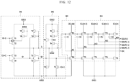
- FIG. 12 is a diagram illustrating a circuit configuration of a k th stage circuit (or k th stage) STG(k) included in a gate driving circuit 13 according to an embodiment of the present disclosure.
- the k th stage circuit STG(k) may include a Q node, a QH node, and a QB node.
- the k th stage circuit STG(k) may include a Q/QH node controller BK1, a QB node controller BK2, a carry output portion BK3, and a scan output portion BK4.
- the Q/QH node controller BK1 may charge the Q node at a first high-level voltage GVDD1 level in response to an input of a previous carry signal C(k-2) and may discharge the Q node at a third low level voltage GVSS3 level in response to an input of a next carry signal C(k+2).
- the Q/QH node controller BK1 may include first to eighth transistors T21 to T28.
- a first transistor T21 and a second transistor T22 may be connected between the Q node and a first high-level voltage line which transfers the first high level voltage GVDD1.
- the first transistor T21 and the second transistor T22 may be serially connected with each other.
- the first transistor T21 and the second transistor T22 may charge the Q node at the first high level voltage GVDD1 level in response to the input of the previous carry signal C(k-2).
- the first transistor T21 may be turned on based on the input of the previous carry signal C(k-2) and may transfer the first high level voltage GVDD1 to a connection node NC2.
- the second transistor T22 may be turned on based on the input of the previous carry signal C(k-2) and may electrically connect the connection node NC2 to the Q node. Accordingly, when the first transistor T21 and the second transistor T22 are simultaneously turned on, the first high level voltage GVDD1 may be supplied to the Q node.
- a fifth transistor T25 and a sixth transistor T26 may be connected with a third high level voltage line which transfers the third high level voltage GVDD3.
- the fifth transistor T25 and the sixth transistor T26 may transfer the third high level voltage GVDD3 to a connection node NC2 in response to the third high level voltage GVDD3.
- the fifth transistor T25 and the sixth transistor T26 may be simultaneously turned on by the third high level voltage GVDD3 and may transfer the third high level voltage GVDD3 to the connection node NC, and thus, may increase a voltage difference between a gate of the first transistor T21 and the connection node NC2.
- the first transistor T21 may be maintained in a completely turn-off state due to a voltage difference between a gate of the first transistor T21 and the connection node NC2. Accordingly, the current leakage of the first transistor T21 and the voltage drop of the Q node caused thereby may be prevented, and thus, a voltage of the Q node may be stably maintained.
- the third high level voltage GVDD3 may be set to a voltage level which is lower than the first high level voltage GVDD1.
- a third transistor T23 and a fourth transistor T24 may be connected between the Q node and a third low level voltage line which transfers the third low level voltage GVSS3.
- the third transistor T23 and the fourth transistor T24 may be serially connected with each other.
- the third transistor T23 and the fourth transistor T24 may discharge the Q node and the QH node at the third low level voltage GVSS3 level in response to an input of the next carry signal C(k+2).
- the fourth transistor T24 may be turned on based on the input of the next carry signal C(k+2) and may discharge the QH node at a third low level voltage GVSS3 level.
- the third transistor T23 may be turned on based on the input of the next carry signal C(k+2) and may electrically connect the Q node with the QH node. Accordingly, when the third transistor T23 and the fourth transistor T24 are simultaneously turned on, each of the Q node and the QH node may be discharged at the third low level voltage GVSS3 level.
- a seventh transistor T27 and an eighth transistor T28 may be connected between the Q node and a first high-level voltage line which transfers the first high level voltage GVDD1 and may be connected between the QH node and the first high level voltage line which transfers the first high level voltage GVDD1.
- the seventh transistor T27 and the eighth transistor T28 may be serially connected with each other.
- the seventh transistor T27 and the eighth transistor T28 may transfer the first high level voltage GVDD1 to the QH node in response to a voltage of the Q node.
- the seventh transistor T27 When the voltage of the Q node has an on level, the seventh transistor T27 may be turned on and may transfer the first high level voltage GVDD1 to a shared node between the seventh transistor T27 and the eighth transistor T28.
- the eighth transistor T28 When the voltage of the Q node has an on level, the eighth transistor T28 may be turned on and may electrically connect the shared node with the QH node. Therefore, when the voltage of the Q node has an on level, the seventh transistor T27 and the eighth transistor T28 may be simultaneously turned on and may transfer the first high level voltage GVDD1 to the QH node. When the first high level voltage GVDD1 is supplied to the QH node, a voltage difference between a gate of the third transistor T23 and the QH node may increase.
- the third transistor T23 may be maintained in a completely turn-off state due to a voltage difference between a gate of the third transistor T23 and the QH node. Accordingly, the current leakage of the third transistor T23 and the voltage drop of the Q node caused thereby may be prevented, and thus, a voltage of the Q node may be stably maintained.
- the Q/QH node controller BK1 may discharge the Q node and the QH node at the third low level voltage GVSS3 level.
- the Q/QH node controller BK1 may further include a first additional transistor T31 and a second additional transistor T32.
- the first additional transistor T31 and the second additional transistor T32 may be connected between the Q node and the third low level voltage line which transfers the third low level voltage GVSS3.
- the first additional transistor T31 and the second additional transistor T32 may be serially connected with each other.
- the first additional transistor T31 and the second additional transistor T32 may discharge the Q node and the QH node at the third low level voltage GVSS3 level.
- the second additional transistor T32 may be turned on and may transfer the third low level voltage GVSS3 to a shared node between the first additional transistor T31 and the second additional transistor T32.
- the first additional transistor T31 may be turned on and may electrically connect the Q node with the QH node. Therefore, in response to the voltage of the QB node, the first additional transistor T31 and the second additional transistor T32 may be simultaneously turned on and may discharge each of the Q node and the QH node at the third low level voltage GVSS3 level.
- the QB node controller BK2 may shift a voltage level of the QB node, based on a voltage level of the Q node.
- the QB node controller BK2 may include first to fifth transistors T41 to T45.
- the second transistor T42 and the third transistor T43 may be connected between a third connection node NC3 and a second high level voltage line which transfers the second high level voltage GVDD2.
- the second transistor T42 and the third transistor T43 may be serially connected with each other.
- the second transistor T42 and the third transistor T43 may transfer the second high level voltage GVDD2 to the third connection node NC3.
- the second transistor T42 may be turned on by the second high level voltage GVDD2 and may transfer the second high level voltage GVDD2 to a shared node between the second transistor T42 and the third transistor T43.
- the third transistor T43 may be turned on by the second high level voltage GVDD2 and may electrically connect the third connection node NC3 with the shared node between the second transistor T42 and the third transistor T43. Therefore, when the second transistor T42 and the third transistor T43 are simultaneously turned on by the second high level voltage GVDD2, the third connection node NC3 may be charged at the second high level voltage GVDD2 level.
- the fourth transistor T44 may be connected between the third connection node NC3 and a second low level voltage line which transfers a second low level voltage GVSS2. In response to a voltage of the Q node, the fourth transistor T44 may transfer the second low level voltage GVSS2 to the third connection node NC3. When the voltage of the Q node has an on level, the fourth transistor T44 may be discharged or reset the third connection node NC3 to the second low level voltage GVSS2.
- the first transistor T41 may be connected between the QB node and the second high level voltage line which transfers the second high level voltage GVDD2. In response to the voltage of the third connection node NC3, the first transistor T41 may transfer the second high level voltage GVDD2 to the QB node. When the voltage of the third connection node NC3 has an on level, the first transistor T41 may be turned on and may charge the QB node at the second high level voltage GVDD2 level.
- the fifth transistor T45 may be connected between the QB node and the third low level voltage line which transfers the third low level voltage GVSS3. In response to the voltage of the Q node, the fifth transistor T45 may transfer the third low level voltage GVSS3 to the QB node. When the voltage of the Q node has an on level, the fifth transistor T45 may be turned on and may discharge the QB node at the third low level voltage GVSS3 level.
- the QB node controller BK2 may discharge the QB node at the third low level voltage GVSS3 level in response to an input of the next carry signal C(k-2). To this end, the QB node controller BK2 may further include a first additional transistor T51.
- the first additional transistor T51 may be connected between the QB node and the third low level voltage line which transfers the third low level voltage GVSS3.
- the first additional transistor T51 may transfer the third low level voltage GVSS3 to the QB node in response to the input of the next carry signal C(k-2).
- the carry output portion BK3 may output a carry clock CRCLK(k) having a gate on voltage as a carry signal C(k) having an on voltage while the Q node is being charged at an on-voltage level, and while the QB node is being charged at an on voltage level, the carry output portion BK3 may output the third low level voltage GVSS3 as the carry signal C(k) having an off voltage.
- the carry output portion BK3 may include a first transistor T81, a second transistor T82, and a boosting capacitor CC.
- the first transistor T81 may be connected between a clock signal line corresponding to the carry clock CRCLK(k) and an output node NO.
- the boosting capacitor CC may be connected between a gate and a source of the first transistor T81.
- the boosting capacitor CC may bootstrap the voltage of the Q node up to a boosting voltage level which is higher than the first high level voltage GVDD1 level, in synchronization with the carry clock CRCLK(k) having the gate on voltage.
- the carry signal C(k) having an on voltage may be quickly charged into the output node NO without distortion. Therefore, the carry signal C(k) having an on voltage may be output from the output node NO.
- the second transistor T82 may transfer the third low level voltage GVSS3 to the output node NO. Accordingly, the carry signal C(k) having an off voltage may be output from the output node NO.
- the scan output portion BK4 may output first to fourth scan clocks SCLK(n-3) to SCLK(n) having the gate on voltage as first to fourth scan signals SCOUT(n-3) to SCOUT(n) having an on voltage while the Q node is being charged at an on voltage level, and while the QB node is being charged at an on voltage level, the scan output portion BK4 may output the first low level voltage GVSS1 as first to fourth scan signals SCOUT(n-3) to SCOUT(n) having an off voltage.
- the scan output portion BK4 may include first to eighth transistors T71 to T78 and first to fourth boosting capacitors CS1 to CS4.
- the first transistor T71 may be connected between a clock signal line corresponding to the first scan clock SCLK(n-3) and a first output node NO1.
- the first boosting capacitor CS1 may be connected between a gate and a source of the first transistor T71.
- the first boosting capacitor CS1 may bootstrap the voltage of the Q node up to a boosting voltage level which is higher than the first high level voltage GVDD1 level, in synchronization with the first scan clock SCLK(n-3) having the gate on voltage.
- the first scan signal SCOUT(n-3) having an on voltage may be quickly charged into the first output node NO1 without distortion.
- the first scan signal SCOUT(n-3) having an on voltage may be output from the first output node NO1.
- the second transistor T72 may transfer the first low level voltage GVSS1 to the first output node NO1. Accordingly, the first scan signal SCOUT(n-3) having an off voltage may be output from the first output node NO1.
- the third transistor T73 may be connected between a clock signal line corresponding to the second scan clock SCLK(n-2) and a second output node NO2.
- the second boosting capacitor CS2 may be connected between a gate and a source of the third transistor T73.
- the second boosting capacitor CS2 may bootstrap the voltage of the Q node up to a boosting voltage level which is higher than the first high level voltage GVDD1 level, in synchronization with the second scan clock SCLK(n-2) having the gate on voltage.
- the second scan signal SCOUT(n-2) having an on voltage may be quickly charged into the second output node NO2 without distortion.
- the second scan signal SCOUT(n-2) having an on voltage may be output from the second output node NO2.
- the fourth transistor T74 may transfer the first low level voltage GVSS1 to the second output node NO2. Accordingly, the second scan signal SCOUT(n-2) having an off voltage may be output from the second output node NO2.
- the fifth transistor T75 may be connected between a clock signal line corresponding to the third scan clock SCLK(n-1) and a third output node NO3.
- the third boosting capacitor CS3 may be connected between a gate and a source of the fifth transistor T75.
- the third boosting capacitor CS3 may bootstrap the voltage of the Q node up to a boosting voltage level which is higher than the first high level voltage GVDD1 level, in synchronization with the third scan clock SCLK(n-1) having the gate on voltage.
- the third scan signal SCOUT(n-1) having an on voltage may be quickly charged into the third output node NO3 without distortion.
- the third scan signal SCOUT(n-1) having an on voltage may be output from the third output node NO3.
- the sixth transistor T76 may transfer the first low level voltage GVSS1 to the third output node NO3. Accordingly, the third scan signal SCOUT(n-1) having an off voltage may be output from the third output node NO3.
- the seventh transistor T77 may be connected between a clock signal line corresponding to the fourth scan clock SCLK(n) and a fourth output node NO4.
- the fourth boosting capacitor CS4 may be connected between a gate and a source of the seventh transistor T77.
- the fourth boosting capacitor CS4 may bootstrap the voltage of the Q node up to a boosting voltage level which is higher than the first high level voltage GVDD1 level, in synchronization with the fourth scan clock SCLK(n) having the gate on voltage.
- the fourth scan signal SCOUT(n) having an on voltage may be quickly charged into the fourth output node NO4 without distortion.
- the fourth scan signal SCOUT(n) having an on voltage may be output from the fourth output node NO4.
- the eighth transistor T78 may transfer the first low level voltage GVSS1 to the fourth output node NO4. Accordingly, the fourth scan signal SCOUT(n) having an off voltage may be output from the fourth output node NO4.
- a high level voltage and a low level voltage may be respectively set to three different (or two) voltage levels. That is, each of the high level voltage and a low level voltage may be set to a plurality of different voltages levels.
- the first high level voltage GVDD1 may be set to 20 V
- the second high level voltage GVDD2 may be set to 16 V
- the third high level voltage GVDD3 may be set to 14 V
- the first low level voltage GVSS1 may be set to - 6 V
- the second low level voltage GVSS2 may be set to -10 V
- the third low level voltage GVSS3 may be set to -12 V
- the first low level voltage GVSS1 and the second low level voltage GVSS2 may be set to the same voltage (for example, -6 V).
- Such numerical values may be merely an embodiment, and levels of a high level voltage and a low level voltage may be differently set according to embodiments.
- FIG. 13 is a diagram illustrating a concept for reducing a time needed for the transfer of a carry signal for sufficiently securing an output time of a touch scan signal in a touch frame according to an embodiment of the present disclosure.
- FIG. 14 is a diagram illustrating driving waveforms of display carry clocks and display scan clocks for generating a display scan signal according to an embodiment of the present disclosure.
- FIG. 15 is a diagram illustrating driving waveforms of touch carry clocks and touch scan clocks for generating a touch scan signal according to an embodiment of the present disclosure.
- FIG. 16 is a diagram illustrating an example where a touch scan signal having an on pulse is applied to only some gate lines by using touch scan clocks, in each of touch screen blocks according to an embodiment of the present disclosure.
- a gate driving circuit 13 may output a display scan signal D-SCAN or a touch scan signal T-SCAN to a display panel by using the stages of FIGs. 9 to 12 described above.
- a plurality of stages may be sequentially activated in operation with respect to display carry clocks CRCLK1 to CRCLK3 (see FIG. 14 ) that changes between a gate on voltage Vgh and a gate off voltage Vgl in a display frame D-Frame and may output the display scan signal D-SCAN to the display panel.
- the plurality of stages may be sequentially activated in operation with respect to touch carry clocks CRCLK1 to CRCLK3 (see FIG. 15 ) swinging between the gate on voltage Vgh and the gate off voltage Vgl in a touch frame T-Frame and may output the touch scan signal T-SCAN to the display panel.
- a one-frame time may be about 8 ms. That is, each of the display frame D-Frame and the touch frame T-Frame may have a time length of about 8 ms.
- a time needed for transferring a carry signal between stages may be relatively more reduced in the touch frame T-Frame than the display frame D-Frame.
- an on-pulse width of each of the touch carry clocks CRCLK1 to CRCLK3 is narrower (it on-time duration being shorter) than an on pulse width of each of the display carry clocks CRCLK1 to CRCLK3.
- the on-pulse width of each of the display carry clocks CRCLK1 to CRCLK3 may be a two horizontal period 2H, and the on pulse width of each of the touch carry clocks CRCLK1 to CRCLK3 may be a one horizontal period 1H.
- one cycle of the display carry clocks CRCLK1 to CRCLK3 may be a 12 horizontal period 12H, and one cycle of the touch carry clocks CRCLK1 to CRCLK3 may be a 3 horizontal period 3H.
- the number of display scan signals D-SCAN having an on pulse should be equal to the number of gate lines, and on pulses of display scan clocks SCLK1 to SCLK12 should be designed to be equal to the number of on pulses of the display scan signals D-SCAN.
- An on-pulse width of each of the display scan clocks SCLK1 to SCLK12 may be equal to an on pulse width of each of the display carry clocks CRCLK1 to CRCLK3.
- the number of touch scan signals T-SCAN having an on pulse may be less than the number of gate lines.
- on pulses of touch scan clocks SCLK1 to SCLK12 may be designed to be synchronized with on-period positions of the touch scan signals T-SCAN. Accordingly, an on pulse of each of the touch scan signals T-SCAN and an on pulse width of each of the touch scan clocks SCLK1 to SCLK12 corresponding thereto may be widely designed to be a 100 horizontal period 100H.
- a first stage (STG(1) of FIG. 10 ) may output a first touch scan signal T-SCAN1 having a first on pulse 100H to a first touch screen block TBLK1 of the display panel according to a first touch scan clock SCLK1 having a gate on voltage Vgh
- a second stage (STG(53) of FIG. 10 ) may output a second touch scan signal T-SCAN53 having a second on pulse 100H to a second touch screen block TBLK2 of the display panel according to a second touch scan clock SCLK5 having the gate on voltage Vgh
- a third stage (STG(105) of FIG. 10 ) may output a third touch scan signal T-SCAN105 having a third on pulse 100H to a third touch screen block TBLK3 of the display panel according to a third touch scan clock SCLK9 having the gate on voltage Vgh.
- a phase of the first touch scan clock SCLK1 may be earlier than that of the second touch scan clock SCLK5, and a phase of the second touch scan clock SCLK5 may be earlier than that of the third touch scan clock SCLK9.
- each of the first to third on pulses may be a 100 horizontal period 100H.
- the first stage (STG(1) of FIG. 10 ) may output the first touch scan signal T-SCAN1 to one first gate line included in the first touch screen block TBLK1 without the first touch scan signal T-SCAN1 being supplied to remaining first gate lines included in the first touch screen block TBLK1
- the second stage (STG(53) of FIG. 10 ) may output the second touch scan signal T-SCAN53 to one second gate line included in the second touch screen block TBLK2 without the second touch scan signal T-SCAN53 being supplied to remaining second gate lines included in the second touch screen block TBLK2
- the third stage (STG(105) of FIG. 10 ) may output the third touch scan signal T-SCAN105 to one third gate line included in the third touch screen block TBLK3 without the third touch scan signal T-SCAN105 being supplied to remaining third gate lines included in the third touch screen block TBLK3.
- one or more stages (STG(2) to STG(52) of FIG. 10 ) arranged between the first stage (STG(1) of FIG. 10 ) and the second stage (STG(53) of FIG. 10 ) may supply one or more touch scan signals T-SCAN2 to T-SCAN52 having no on pulse to one or more gate lines arranged between the first and second gate lines, based on a touch scan clock having a gate off voltage Vgl.
- one or more stages (STG(54) to STG(104) of FIG. 10 ) arranged between the second stage (STG(53) of FIG. 10 ) and the third stage (STG(105) of FIG. 10 ) may supply one or more touch scan signals T-SCAN54 to T-SCAN104 having no on pulse to one or more gate lines arranged between the second and third gate lines, based on the touch scan clock having the gate off voltage Vgl.
Landscapes
- Engineering & Computer Science (AREA)
- General Engineering & Computer Science (AREA)
- Theoretical Computer Science (AREA)
- Human Computer Interaction (AREA)
- Physics & Mathematics (AREA)
- General Physics & Mathematics (AREA)
- Computer Networks & Wireless Communication (AREA)
- Control Of Indicators Other Than Cathode Ray Tubes (AREA)
- Liquid Crystal Display Device Control (AREA)
Abstract
Description
- The present disclosure relates to a touch sensing display apparatus.
- Touch sensors are simple in configuration and small in number of abnormal operations and provide the convenience of users, and thus, are being applied to various display apparatuses.
- Touch sensing display apparatuses may alternately drive a display frame and a touch frame, based on a time division scheme, and thus, may sense a touch input while an image is being displayed on a screen. In such touch sensing display apparatuses, because a conventional gate driving circuit is intactly used for time division driving, a scan output time for touch sensing is insufficient, and due to this, it is difficult to increase touch performance.
- To overcome the aforementioned problem of the related art, the present disclosure may provide a touch sensing display apparatus which may sufficiently secure a scan output time for touch sensing to enhance touch performance.
- To achieve these objects and other advantages and in accordance with the purpose of the disclosure, as embodied and broadly described herein, a touch sensing display apparatus includes a display panel where display driving of the display panel to display an image and touch sensing driving of the display panel to sense touch of the display panel are alternately implemented at a predetermined period of time. This means that the display panel is configured to be switched between a non-touch driving mode and a touch driving mode, wherein in the non-touch driving mode, the display panel is configured to display an image in all (time) frames, each frame being a display frame, wherein in the touch-driving mode, the display panel is configured to display an image in a display frame and to sense a touch of the display panel in a touch frame, wherein the display frame and the touch frame in the touch-driving mode are alternately performed at predetermined periods of time. The touch sensing display apparatus further comprises a gate driving circuit including a plurality of stages whose operations are sequentially activated (meaning configured to be sequentially activated during operations) to drive gate lines of the display panel, wherein each of the plurality of stages is activated in operation according to a display carry clock having a voltage level that changes between a gate on voltage and a gate off voltage in a display frame and output a display scan signal to the display panel during the display driving (displaying of the image), and wherein each of the plurality of stages is activated in operation according to a touch carry clock changing between the gate on voltage and the gate off voltage in a touch frame and output a touch scan signal to the display panel during the touch sensing driving (sensing of the touch), and an on pulse width of the touch carry clock while the touch carry clock is at the gate on voltage is narrower than an on pulse width of the display carry clock while the display carry clock is at the gate on voltage.
- An on pulse is referred to a first logic state of a digital signal that is opposite to an off pulse width being a second logic state of the digital signal. The sum of on pulse and off pulse may define a time period of the signal.
- An on pulse width is the time duration between two adjacent edges of the on pulse.
- A frame herein is referred to a time frame. One frame may include a vertical active period where new image data is scanned or refreshed or updated. One Frame may additionally include a vertical blank period where scanning of the image data is not performed.
- The displaying of the image, herein also referred to as display driving, that for instance is a not-touch driving mode, may be performed in a vertical active period of a display frame.
- The sensing of the touch, herein also referred to as touch sensing driving, that for instance is a touch driving mode, may be performed in a vertical active period of a touch frame.
- An external compensation operation, hereinafter also referred to as external compensation driving, may be performed in a vertical blank period of each of the display frame and the touch frame. The external compensation driving may be for sensing a device characteristic value (a threshold voltage and electron mobility of a driving transistor and a threshold voltage of a light emitting device) of a pixel.
- In the non-touch driving mode, all frames may be display frames for display driving (displaying the image that may include external compensation). On the other hand, in the touch driving mode, a display frame for display driving and a touch frame for touch sensing driving may be alternately performed (implemented) at a period of a certain time. The certain time may be a one-frame time (duration) or it may be a plurality of frame times, e.g. several frames.
- Preferably, a touch frame is after the display frame. Here, one display frame may be arranged between two touch frames. Alternatively, a plurality of adjacent display frames may be arranged (on-block) between two touch frames. Alternatively, a plurality of adjacent display frames may be arranged (on-block) between adjacent touch frames.
- The non-touch driving mode of the touch sensing display apparatus, preferably the display panel of the touch sensing display apparatus may be switched into a touch driving mode of the touch sensing display apparatus, preferably the display panel of the touch sensing display apparatus and vice versa. This switching may be performed based on a signal that is generated from the timing controller.
- In certain implementations, the non-touch driving mode may be referred to as display driving mode.
- In certain implementations, the touch driving mode may be referred to as display-and-touch driving mode.
- Each of the non-touch driving mode and the touch driving mode may be switched based on whether there is a touch input, and/or a mode selection information about a user, and/or a distance information between a display apparatus and a user.
- The non-touch driving mode, e.g. that may also be referred to as display driving mode, may be a driving mode for performing a display operation and an external compensation operation, preferably for displaying of the image.
- The touch driving mode, e.g. that may also be referred to as display-and-touch driving mode, may be a driving mode for performing a touch sensing operation in addition to a display operation and an external compensation operation.
- In the non-touch driving mode, all frames may be display frames for display driving. On the other hand, in the touch driving mode, a display frame for display driving and a touch frame for touch sensing driving may be alternately performed at a period of a certain time. For example, a touch frame is after the display frame. Here, the certain time may be a one-frame time, and in this case, one display frame may be arranged between adjacent touch frames. However, the inventive concept is not limited thereto. The certain time may be a several-frame times, and in this case, a plurality of display frames may be arranged between adjacent touch frames.
- An on pulse width of the touch scan signal that turns on pixels of the display panel during the touch frame may be wider than an on pulse width of the display scan signal that turns on the pixels of the display panel during the display frame.
- The display panel may comprise a plurality of touch screen blocks, each may be configured to be individually driven.
- The plurality of stages may comprise a first stage of the plurality stages that is configured to output a first touch scan signal having a first on pulse to a first touch screen block of the display panel during the touch frame based on a first touch scan clock having the gate on voltage, the first touch screen block including a first plurality of rows of pixels.
- The first stage may supply the first touch scan signal to one first gate line included in the first touch screen block without the first touch scan signal being supplied to remaining first gate lines included in the first touch screen block.
- The plurality of stages may comprise a second stage of the plurality stages that may output a second touch scan signal having a second on pulse to a second touch screen block of the display panel during the touch frame based on a second touch scan clock having the gate on voltage, the second touch screen block including a second plurality of rows of pixels.
- A phase of the first touch scan clock may be different from a phase of the second touch scan clock.
- A length of the first on pulse of the first touch scan signal may be equal to a length of the second on pulse of the second touch scan signal.
- The second stage may supply the second touch scan signal to one second gate line included in the second touch screen block without the second touch scan signal being supplied to remaining second gate lines included in the second touch screen block.
- The plurality of stages further comprises one or more third stages arranged between the first stage and the second stage, the one or more third stages configured to supply a third touch scan signal having an off period but no on pulse to one or more third gate lines arranged between the one first gate line and the one second gate line during the touch frame based on a touch scan clock having a gate off voltage.
- A sensing circuit may be configured to sense a voltage of a source node of a representative pixel that is on a substrate of the display panel according to the touch scan signal, the sensed voltage indicative of whether a touch input is applied to the display panel during the touch frame.
- The representative pixel may comprise a storage capacitor and a driving transistor, the driving transistor may include a source electrode connected with the source node and a gate electrode connected with a gate node,
- The gate node may comprise a first conductive pattern that faces the source node with one or more insulation layers between the gate node and the source node and may be a first electrode of the storage capacitor.
- The gate node may comprise a second conductive pattern that is connected with the first conductive pattern through a contact hole passing through the one or more insulation layers.
- The source node may comprise a third conductive pattern on the one or more insulation layers and may be a second electrode of the storage capacitor.
- The first conductive pattern may be closest to the substrate among the first conductive pattern, the second conductive pattern, and the third conductive pattern.
- The second conductive pattern may be on the one or more insulation layers and may comprise a same material as a material of the third conductive pattern.
- During the touch frame, a driving current of the representative pixel and the voltage of the source node may change according to the touch input.
- A first driving current of the representative pixel while there is a touch input at a position of the representative pixel may be less than a second driving current of the representative pixel while there is no touch input at the position of the representative pixel.
- A voltage of the source node of the representative pixel while there is a touch input at a position of the representative pixel may be less than a voltage of the source node of the representative pixel while there is no touch input at the position of the representative pixel.
- The gate driving circuit may further include a dummy stage that is disposed at a previous stage that is prior to a first stage of the plurality of stages.
- The gate driving circuit may further include a gate driving voltage line that may be configured to transfer a high-level voltage and a low-level voltage, supplied from a power supply circuit, to the plurality of stages and the dummy stage.
- The high-level voltage and the low-level voltage may each be respectively set to a plurality of different voltage levels.
- The representative pixel may comprise a driving transistor including a source electrode connected with the source node and a gate electrode connected with a gate node.
- The gate node may be closer to the substrate than the source node.
- The representative pixel may include a gate node that is electrically disconnected from the source node.
- A number of the plurality of stages may be a quarter of a number of the gate lines.
- The present embodiments may realize the following effects.
- According to the present embodiments, the number of additional elements for touch sensing may be reduced, and touch sensing performance may be enhanced.
- According to the present embodiments, an on-pulse width of a carry clock may be designed narrower in touch sensing driving than display driving, and thus, a transfer time of a carry signal may be shortened in a touch frame. In the present embodiments, a time capable of being allocated for an output of a touch scan signal in a touch frame may be long secured in proportion to a reduction in transfer time of the carry signal, and thus, touch performance may increase.
- The effects according to the present disclosure are not limited to the above examples, and other various effects may be included in the specification.
- The accompanying drawings, which are included to provide a further understanding of the disclosure and are incorporated in and constitute a part of this application, illustrate embodiment(s) of the disclosure and together with the description serve to explain the principle of the disclosure. In the drawings:
-
FIG. 1 is a block diagram illustrating a touch sensing display apparatus according to an embodiment of the present disclosure; -
FIG. 2 is a diagram illustrating a connection configuration of a pixel array and a source driver integrated circuit according to an embodiment of the present disclosure; -
FIG. 3 is a diagram illustrating a connection configuration of a pixel and a sensing circuit according to an embodiment of the present disclosure; -
FIGs. 4 and 5 are diagrams illustrating a concept for sensing a variation of a source node voltage of a pixel based on a touch input according to an embodiment of the present disclosure; -
FIG. 6 is a diagram illustrating a cross-sectional structure of a circuit unit of a representative pixel capable of touch sensing according to an embodiment of the present disclosure; -
FIG. 7 is a diagram illustrating a voltage variation of each of a gate node and a source node of a driving transistor, based on whether there is a touch input according to an embodiment of the present disclosure; -
FIGs. 8 and9 are diagrams illustrating an example where display driving and touch sensing driving are implemented based on a time division scheme according to an embodiment of the present disclosure; -
FIGs. 10 and11 are diagrams schematically illustrating a stage configuration of a gate driving circuit according to an embodiment of the present disclosure; -
FIG. 12 is a diagram illustrating a circuit configuration of a kth stage circuit included in a gate driving circuit according to an embodiment of the present disclosure; -
FIG. 13 is a diagram illustrating a concept for reducing a time needed for the transfer of a carry signal for sufficiently securing an output time of a touch scan signal in a touch frame according to an embodiment of the present disclosure; -
FIG. 14 is a diagram illustrating driving waveforms of display carry clocks and display scan clocks for generating a display scan signal according to an embodiment of the present disclosure; -
FIG. 15 is a diagram illustrating driving waveforms of touch carry clocks and touch scan clocks for generating a touch scan signal according to an embodiment of the present disclosure; and -
FIG. 16 is a diagram illustrating an example where a touch scan signal having an on pulse is applied to only some gate lines by using touch scan clocks, in each of touch screen blocks according to an embodiment of the present disclosure. - Hereinafter, exemplary embodiments of the present disclosure will be described in detail with reference to the accompanying drawings. In the specification, in adding reference numerals for elements in each drawing, it should be noted that like reference numerals already used to denote like elements in other drawings are used for elements wherever possible. In the following description, when the detailed description of the relevant known function or configuration is determined to unnecessarily obscure the important point of the present disclosure, the detailed description will be omitted.
- A scan signal (or a gate signal) applied to pixels may swing between a gate on voltage and a gate off voltage. The gate on voltage may be set to a voltage which is higher than a threshold voltage of a transistor, and the gate off voltage may be set to a voltage which is lower than the threshold voltage of the transistor. The transistor may be turned on in response to the gate on voltage and may be turned off in response to the gate off voltage. In N-channel transistors, the gate on voltage may be a gate high voltage (VGH), and the gate off voltage may be a gate low voltage (VGL). In P-channel transistors, the gate on voltage may be the gate low voltage (VGL), and the gate off voltage may be the gate high voltage (VGH).
-
FIG. 1 is a block diagram illustrating a touch sensing display apparatus according to an embodiment of the present disclosure.FIG. 2 is a diagram illustrating a connection configuration of a pixel array and a source driver integrated circuit according to an embodiment of the present disclosure. - Referring to
FIGs. 1 and2 , the touch sensing display apparatus according to the present embodiment may include adisplay panel 10, atiming controller 11, adata driving circuit 12, agate driving circuit 13, and a sensing circuit SU. The sensing circuit SU may be embedded in thedata driving circuit 12, but is not limited thereto. - In a screen displaying an input image in the
display panel 10,first signal lines 14 extending in a column direction (or a vertical direction) may intersect withsecond signal lines 15 extending in a row direction (or a horizontal direction), and a plurality of pixels P may be respectively provided in a plurality of intersection areas and may be arranged as a matrix type to configure a pixel array. Thefirst signal lines 14 may include a plurality ofdata lines 14A through which data voltages are supplied and a plurality ofreference voltage lines 14B through which a reference voltage is supplied. Thereference voltage lines 14B may connect the pixels P with the sensing circuit SU and may be referred to as a sensing line. Thesecond signal lines 15 may be gate lines through which scan signals are supplied. - The pixel array may include a plurality of pixel set lines PL. Here, the pixel set line PL may not denote a physical signal line but may be defined as a pixel set of pixels of one line arranged adjacent to one another in a horizontal direction or defined as a pixel block of pixels of one line. The pixels P may be grouped into a plurality of groups and may implement various colors. When a pixel group for implementing colors is defined as a unit pixel UPXL, one unit pixel UPXI, may include red (R), green (G), blue (B), and white (W) pixels. The R, G, B, and W pixels configuring the one-unit pixel UPXI, may be arranged adjacent to one another in a horizontal direction and may be designed to share the same
reference voltage line 14B, and thus, the pixel array may be simplified. - The
timing controller 11 may be configured to provide a signal that switches (converts) a non-touch driving mode of the touch sensing display apparatus, preferably the display panel of the touch sensing display apparatus into a touch driving mode of the touch sensing display apparatus, preferably the display panel of the touch sensing display apparatus and vice versa. In certain implementations, the non-touch driving mode may be referred to as display driving mode. In certain implementations, the touch driving mode may be referred to as display-and-touch driving mode. Alternatively, and/or additionally, each of the non-touch driving mode and the touch driving mode may be switched based on whether there is a touch input, and/or a mode selection information about a user, and/or a distance information between a display apparatus and a user. The non-touch driving mode, e.g. that may also be referred to as display driving mode, may be a driving mode for performing a display operation and an external compensation operation, preferably for displaying an image. The touch driving mode, e.g. that may also be referred to as non-display driving mode, may be a driving mode for further performing a touch sensing operation in addition to a display operation and an external compensation operation. - In the non-touch driving mode, all frames may be display frames for display driving. On the other hand, in the touch driving mode, a display frame for display driving and a touch frame for touch sensing driving may be alternately performed at a period of a certain time. For example, a touch frame is after the display frame. Here, the certain time may be a one-frame time, and in this case, one display frame may be arranged between two (adjacent) touch frames. However, the inventive concept is not limited thereto. The certain time may be a several-frames (frame times,) and in this case, a plurality of (adjacent) display frames may be arranged (on-block) between two (adjacent) touch frames.
- One frame may include a vertical active period where new image data DATA is scanned (or refreshed or updated) and a vertical blank period where scanning of the image data DATA is not performed. Display driving, e.g. the displaying of the image in the non-touch driving mode and the touch-driving mode, may be performed in a vertical active period of a display frame, and touch sensing driving, e.g. the sensing of the touch in the touch driving mode, may be performed in a vertical active period of a touch frame. External compensation driving, e.g. the external compensation operation, may be performed in a vertical blank period of each of the display frame and the touch frame. The external compensation driving may be for sensing a device characteristic value (a threshold voltage and electron mobility of a driving transistor and a threshold voltage of a light emitting device) of a pixel P.
- The
timing controller 11 may correct digital video data input from a host system by using a compensation value based on a pixel sensing value based on external compensation driving, and then, may supply corrected image data DATA to thedata driving circuit 12. Thetiming controller 11 may receive a timing signal such as a vertical synchronization signal Vsync, a horizontal synchronization signal Hsync, a data enable signal DE, and a dot clock DCLK from the host system to generate a gate timing control signal GDC for controlling an operation timing of thegate driving circuit 13 and a data timing control signal DDC for controlling an operation timing of thedata driving circuit 12. - The
timing controller 11 may compare a predetermined reference value with a touch sensing value based on a touch sensing operation to obtain coordinate information about a touch input position and may transfer the coordinate information to the host system. The host system may execute a touch application corresponding to the coordinate information. - The
data driving circuit 12 may include one or more source driving ICs SDIC. Each of the source driving Ics SDIC may include a latch array, a plurality of digital-to-analog converters DAC respectively connected to the data lines 14A, a plurality of sensing circuits SU respectively connected to the sensing lines 14B, a plurality of multiplex switches SS which selectively connect the sensing circuits SU to a plurality of analog-to-digital converters ADC, and a shift register SR which sequentially turns on the multiplex switches SS. - The latch array may latch the corrected image data DATA input from the
timing controller 11, based on the data control signal DDC, and may supply the latched image data DATA to the digital-to-analog converters DAC. The digital-to-analog converters DAC may convert the latched image data DATA into display data voltages and may supply the display data voltages to the data lines 14A. In external compensation driving, the digital-to-analog converters DAC may generate a predetermined external sensing data voltage and may supply the external sensing data voltage to the data lines 14A. In touch sensing driving, the digital-to-analog converters DAC may generate a predetermined touch driving data voltage and may supply the touch driving data voltage to the data lines 14A. - The sensing circuit SU may be used in common in external compensation driving and touch sensing driving, and thus, a separate touch sensing circuit for touch sensing may be removed. Because touch sensing is possible without the separate touch sensing circuit, the source driving IC may be simplified, and thus, power consumption and the manufacturing cost may be reduced.
- The sensing circuit SU may supply a reference voltage Vpre to the
sensing line 14B, based on the data control signal DDC, or may sample a touch sensing value or a device characteristic sensing value input through thesensing line 14B and may supply a sampled touch sensing value or device characteristic sensing value to the analog-to-digital converter ADC. - The analog-to-digital converter ADC may receive a clock signal, convert the touch sensing value or the device characteristic sensing value, input from the sensing circuits SU, into a digital sensing signal SLV and may transfer the digital sensing signal SLV to the
timing controller 11. - The
gate driving circuit 13 may generate a scan signal (e.g a scan signal SCAN ofFIG. 3 ) suitable for display driving, external compensation driving, and touch sensing driving, based on the gate control signal GDC by using a stage circuit STG, and then, may supply the scan signal SCAN to the gate lines 15. The scan signal may include a display scan signal for display driving, an external sensing scan signal for external compensation driving, and a touch scan signal for touch sensing driving. An on pulse of the display scan signal may correspond to a supply timing of a display data voltage. An on pulse of the external sensing scan signal may correspond to a supply timing of an external sensing data voltage. An on pulse of the touch scan signal may correspond to a supply timing of a touch driving data voltage. - The gate control signal GDC may include a plurality of scan clocks and a plurality of carry clocks. An on-pulse width of the carry clock, e.g. a display carry clock or a touch carry clock, may be designed narrower in touch sensing driving than display driving, and thus, a transfer time of a carry signal may be shortened in a touch frame. A time capable of being allocated for an output of a touch scan signal in a touch frame may increase in proportion to a reduction in transfer time of the carry signal, and thus, touch performance may be enhanced.
-
FIG. 3 is a diagram illustrating a connection configuration of a pixel P and a sensing circuit SU according to an embodiment of the present disclosure. - Referring to
FIG. 3 , the pixel P may be implemented in a structure capable of an external compensation operation and a touch sensing operation. The pixel P may include a light emitting device OLED, a driving transistor DT, a storage capacitor Cst, a first switch transistor ST1, and a second switch transistor ST2. The transistors DT, ST1, and ST2 may each be implemented as a thin film transistor (TFT). TFTs may be implemented as a P type, an N type, or a hybrid type where the P type and the N type are provided in common. Also, a semiconductor layer of a TFT may include amorphous silicon, polysilicon, or oxide. - The light emitting device OLED may include an anode electrode connected to a source node DTS, a cathode electrode connected to an input terminal of a low-level driving voltage EVSS, and an organic compound layer disposed between the anode electrode and the cathode electrode. The organic compound layer may include a hole injection layer (HIL), a hole transport layer (HTL), an emission layer (EML), an electron transport layer (ETL), and an electron injection layer (EIL).
- The driving transistor DT may control a level of a drain-source current (hereinafter referred to as Ids) of the driving transistor DT input to the light emitting device OLED, based on a gate-source voltage (hereinafter referred to as Vgs) thereof. The driving transistor DT may include a gate electrode connected with a gate node DTG, a drain electrode connected with an input terminal of a high-level driving voltage EVDD, and a source electrode connected with a source node DTS.
- The storage capacitor Cst may be connected between the gate node DTG and the source node DTS and may hold the gate-source voltage of the driving transistor DT during a predetermined period.
- The first switch transistor ST1 may electrically connect a
data line 14A with the gate node DTG, based on a scan signal SCAN from agate line 15, and may allow a data voltage Vdata to be charged into the gate node DTG. The first switch transistor ST1 may include a gate electrode connected with thegate line 15, a drain electrode connected with thedata line 14A, and a source electrode connected with the gate node DTG. - The second switch transistor ST2 may electrically connect the source node DTS with the
sensing line 14B, based on the scan signal SCAN, and thus, may allow a reference voltage Vpre to be charged into the source node DTS. Also, the second switch transistor ST2 may allow a source node voltage, corresponding to the Ids of the driving transistor DT, to be charged into a line capacitor LCa of thesensing line 14B. The second switch transistor ST2 may include a gate electrode connected with thegate line 15, a drain electrode connected with thesensing line 14B, and a source electrode connected with the source node DTS. - Referring to
FIG. 3 , the sensing circuit SU may be implemented as a voltage sensing type. - The sensing circuit SU may be for sensing a voltage stored in the line capacitor Lca of the
sensing line 14B and may include a reference voltage control switch SW1, a sampling switch SW2, and a sample and hold unit S/H. The reference voltage control switch SW1 may be turned on and may connect an input terminal of the reference voltage Vpre with thesensing line 14B, based on the reference control voltage signal SPRE. The sampling switch SW2 may be turned on and may connect thesensing line 14B with the sample and hold unit S/H, based on the sampling control signal SAM. - When the driving transistor DT is degraded or there is a touch input, the Vgs of the driving transistor DT may vary, and thus, the Ids of the driving transistor DT may vary. A voltage of the source node DTS of the driving transistor DT may vary based on a level of the Ids of the driving transistor DT. While the second switch transistor ST2 is turned on, the voltage of the source node DTS of the driving transistor DT may be stored in the line capacitor Lca of the
sensing line 14B. The sample and hold unit S/H may sample and hold the voltage of the source node DTS of the driving transistor DT stored in the line capacitor Lca of thesensing line 14B while the sampling switch SW2 is turned on, and then, may transfer a sampled voltage to the analog-to-digital converter ADC. -
FIGs. 4 and 5 are diagrams illustrating a concept for sensing a variation of a source node voltage of a pixel based on a touch input (e.g. in a touch driving mode) according to an embodiment of the present disclosure. - The principle that a touch input is sensed in the touch sensing display apparatus according to the present embodiment will be described below with reference to
FIGs. 4 and 5 . - When a touch input object such as a finger contacts a screen of a display panel in a state where a Vgs of a driving transistor is set to a difference voltage between a touch driving data voltage and a reference voltage, the Vgs of the driving transistor may be reduced by a touch capacitor Ctouch between the touch input object and the driving transistor. The touch capacitor Ctouch may be a capacitive capacitor between the touch input object and a gate node DTG of the driving transistor. When the Vgs of the driving transistor is reduced, an Ids of the driving transistor may decrease, and thus, whether there is a touch input may be determined based on that a source node voltage Vs of the driving transistor varies between a pixel touched by the touch input object and an untouched pixel. According to a TFT current formula, the Ids may be proportional to the square of Vgs. Accordingly, even when the amount of Vgs variation based on a touch input is small, the Ids may be amplified, and thus, the source node voltage Vs may be quickly shifted, thereby enhancing touch sensing performance. In
FIG. 5 , "Vg" may denote a gate node voltage of the driving transistor. -
FIG. 6 is a diagram illustrating a cross-sectional structure of a circuit unit of a representative pixel P capable of touch sensing according to an embodiment of the present disclosure. - Because an area contacting a touch input object is far greater than an area occupied by one pixel, the touch sensing apparatus according to the present embodiment may sense a touch input with respect to only some pixels (hereinafter referred to as representative pixels), and thus, a touch sensing period may be shortened, thereby enhancing a touch report rate.
- Referring to
FIG. 6 , the representative pixel P may include an emission portion EP which displays an image and a circuit unit CP which does not display an image. The emission portion EP of the representative pixel P may include the light emitting device OLED ofFIG. 3 . The circuit unit CP of the representative pixel P may include the driving transistor DT, the storage capacitor Cst, the first switch transistor ST1, and the second switch transistor ST2 ofFIG. 3 . - The circuit unit CP of the representative pixel P, as in
FIG. 6 , may include insulation layers BUF, GI, and OC and conductive patterns M1, M2, and PXL stacked on a substrate GLS. In inputting a touch, as Vgs of the driving transistor increases, touch sensing performance may increase. To this end, a gate node connected with the gate electrode of the driving transistor is disposed closer to the substrate GLS than a source node connected with the source electrode of the driving transistor. Therefore, reactivity on a touch input may be improved. Also, because the source node of the driving transistor is connected with an internal capacitor of the light emitting device, when the source node is disposed closer to the substrate GLS than the gate node, a variation of Vgs (i.e., reactivity on a touch input) corresponding to the touch input may be very small, and thus, may be unsuitable for touch sensing. The internal capacitor of the light emitting device may be a capacitor which is between an anode electrode PXL and a cathode electrode. - An array configuration of the representative pixel P will be described below in detail with reference to
FIG. 6 . - A voltage of a source node DTS of the representative pixel P may be a target for touch sensing. The representative pixel P may include a gate node DTG which is electrically disconnected from the source node DTS. The gate node DTG may include a first conductive pattern M1, which faces the source node DTS with one or more insulation layers GI and BLTF therebetween and is one electrode of the storage capacitor Cst, and a second conductive pattern M2 which is connected with the first conductive pattern M1 through a first contact hole CH1 passing through the insulation layers GI and BUF. Also, the source node DTS may be a third conductive pattern M3 which is disposed on the insulation layers GI and BUF and is the other electrode of the storage capacitor Cst. In this case, the first conductive pattern M1 among the first conductive pattern M1, the second conductive pattern M2, and the third conductive pattern M3 may be disposed closest to the substrate GLS.
- That is, the first conductive pattern M1 formed close to the substrate GLS may function as a touch electrode, and moreover, may function as a light blocking pattern. The first conductive pattern M1 may block external light which is incident on a semiconductor layer ACT of the driving transistor, thereby preventing a characteristic value of the driving transistor from being degraded by the external light.
- The first conductive pattern M1 may be covered by a buffer insulation layer BLTF and a gate insulation layer GI and may be electrically connected with the second conductive pattern M2, disposed on the gate insulation layer GI, through the first contact hole CH1. The second conductive pattern M2 may configure the gate electrode of the driving transistor.
- The third conductive pattern M3 which is the other electrode of the storage capacitor Cst may be disposed on the first conductive pattern M1 with the buffer insulation layer BUF and the gate insulation layer GI therebetween. The third conductive pattern M3 may include the same material as that of the second conductive pattern M2 and may configure the same layer along with the second conductive pattern M2. The source electrode of the driving transistor may be formed by providing a conductivity of the semiconductor layer ACT or stacking a conductive layer on the semiconductor layer ACT and may be electrically connected with the third conductive pattern M3 through a contact hole.
- The second conductive pattern M2 and the third conductive pattern M3 may be covered by a planarization layer OC, and the anode electrode PXL of the light emitting device may be formed on the planarization layer OC. Although not shown, the source node DTS of the driving transistor and the anode electrode PXL of the light emitting device may be electrically connected with each other through a contact hole passing through the planarization layer OC.
-
FIG. 7 is a diagram illustrating a voltage variation of each of a gate node and a source node of a driving transistor, based on whether there is a touch input (e.g. in a touch driving mode) according to an embodiment of the present disclosure. - Referring to
FIG. 7 , a touch input corresponding to representative pixels may be sensed in an on-pulse period ON of a touch scan signal T-SCAN. OFF inFIG. 7 refers to an off-pulse period. In response to the touch scan signal T-SCAN, a touch driving data voltage may be applied to a gate node DTG of a driving transistor and a reference voltage Vpre may be applied to a source node DTS of the driving transistor, and thus, the driving transistor may be turned on and Ids may flow in the driving transistor. - When a touch input is received at a first timing t1 of the on-pulse period, Ids1 corresponding to Vgs1 may flow in the driving transistor. The Ids1 of the driving transistor may be less than Ids2 of when there is no touch input. In other words, Ids1 of a first representative pixel corresponding to a position at which there is a touch input may be less than Ids2 of a second representative pixel corresponding to a position at which there is no touch input.
- When touch sensing is performed at a second timing t2 of the on-pulse period, a voltage of the source node DTS of the driving transistor may be sensed as Vsen based on Ids1. The Vsen of the driving transistor may be less than Vsen' based on Ids2 of when there is no touch input. In other words, Vsen of the first representative pixel corresponding to a position at which there is a touch input may be less than Vsen' of the second representative pixel corresponding to a position at which there is no touch input.
- Accordingly, whether there is a touch input corresponding to representative pixels may be determined based on a difference between Vsen and Vsen' which are a voltage of the source node DTS of the driving transistor.
-
FIGs. 8 and9 are diagrams illustrating an example where display driving (display driving mode, e.g. in the non-touch driving mode) and touch sensing driving (touch driving mode) are implemented based on a time division scheme. - Referring to
FIG. 8 , a display frame D-Frame for display driving and a touch frame T-Frame for touch sensing driving may be alternated. The touch frame T-Frame may be arranged between two display frames D-Frame, the display frames D-Frame supposed to be adjacent. Display driving and touch sensing driving may be alternately implemented at a predetermined period of time in the display panel in the touch-driving mode. - Display driving may be for writing image data in all pixels P of a display panel to update an image and may be performed in a vertical active period of the display frame D-Frame. Touch sensing driving may be performed in a vertical active period of the touch frame T-Frame, and because touch sensing driving is performed on the representative pixels P but not the remaining pixels P, a time allocated to touch sensing may be secured to be longer than if all of the pixels of the display panel are sensed. Because the time allocated to touch sensing is long, a touch sensing period may be shortened, and a touch report rate may be enhanced.
- Furthermore, external compensation driving may be performed in a vertical blank period of each of the display frame D-Frame and the touch frame T-Frame.
- Referring to
FIG. 9 , a screen of a display panel may be divided into a plurality of touch screen blocks TBLK, and a touch input may be sensed by touch screen block TBLK units. Each of the touch screen blocks TBLK may include a plurality of pixel set lines PL1 to PLn, and one of the pixel set lines PL1 to PLn in each touch screen block TBLK may be configured with representative pixels. That is, each of the touch screen blocks TBLK includes a plurality of rows of pixels. The number of rows of pixel in each touch screen blocks TBLK may be equal. However, there may be implementations at which the number of rows of pixel in each touch screen blocks TBLK may be different. - A gate driving circuit may apply a display scan signal D-SCAN to all pixels in display frames D-Frame and may apply a touch scan signal T-SCAN to representative pixels in touch frames T-Frame. An on-pulse width PW1 of the touch scan signal T-SCAN may be wider than an on pulse width PW2 of the display scan signal D-SCAN. Because the on-pulse width PW1 of the touch scan signal T-SCAN is wide compared to the width of the on-pulse of the display scan signal D-SCAN, touch sensing performance for the touch screen blocks TBLK may be enhanced.
-
FIGs. 10 and11 are diagrams schematically illustrating a stage configuration of agate driving circuit 13. - Referring to
FIGs. 10 and11 , thegate driving circuit 13 may include first to kth stage circuits STG(1) to STG(k), a gate drivingvoltage line 131, and aclock signal line 132. Also, thegate driving circuit 13 may further include a dummy stage circuit (or dummy stage) DST1 which is disposed at a previous stage with respect to the first stage circuit STG(1). - The gate driving
voltage line 131 may transfer a high level voltage GVDD and a low level voltage GVSS, supplied from a power supply circuit (not shown), to the first to kth stage circuits STG(1) to STG(k) and the dummy stage circuit DST1. In the present embodiment, the gate drivingvoltage line 131 may include two high level voltage lines which respectively transfer a first high-level voltage GVDD1 and a second high level voltage GVDD2 having different voltage levels and three low level voltage lines which respectively transfer a first low-level voltage GVSS1, a second low level voltage GVSS2, and a third low level voltage GVSS3 having different voltage levels. However, this may be merely an embodiment, and the number of voltage lines included in the gate drivingvoltage line 131 may vary. - The
clock signal line 132 may transfer a plurality of clock signals (for example, carry clock signals CRCLK (being a touch carry clock in the touch driving mode and a display carry clock in the non-touch driving mode, see alsoFigs. 14 and15 ) and scan clock signals SCLK), supplied from thetiming controller 11, to the first to kth stage circuits STG(1) to STG(k) and the dummy stage circuit DST1. - The carry clock signals CRCLK may be implemented as first to third carry clocks CRCLK1, CRCLK2, and CRCLK3 having different phases, but are not limited thereto. The first to third carry clocks CRCLK1, CRCLK2, and CRCLK3 may be shifted in phase while swinging between a gate on voltage and a gate off voltage. The first to third carry clocks CRCLK1, CRCLK2, and CRCLK3 may be respectively supplied to the first to kth stage circuits STG(1) to STG(k) through first to third carry clock lines 132-1, 132-2, and 132-3. Each of the first to kth stage circuits STG(1) to STG(k) may receive one of the first to third carry clocks CRCLK1, CRCLK2, and CRCLK3, based on a phase sequence scheme, and may output carry signals C(1) to C(k) corresponding to the received carry clock. Each of the first to kth stage circuits STG(1) to STG(k) may be activated in stage operation, based on a previous carry signal.
- The scan clock signals SCLK may be implemented as first to twelfth scan clocks SCLK1 to SCLK12 having different phases, but are not limited thereto. The first to twelfth scan clocks SCLK1 to SCLK12 may be shifted in phase while swinging between the gate on voltage and the gate off voltage. The first to twelfth scan clocks SCLK1 to SCLK12 may be respectively supplied to the first to kth stage circuits STG(1) to STG(k) through first to twelfth scan clock lines 232-1 to 232-12. Each of the first to kth stage circuits STG(1) to STG(k) may receive one of the first to twelfth scan clocks SCLK1 to SCLK12, based on the phase sequence scheme, and may output scan signals SCOUT(1) to SCOUT(n) corresponding to the received scan clock. Each of the first to kth stage circuits STG(1) to STG(k) may be activated in stage operation, based on a previous carry signal. The dummy stage circuit DST1 may be activated in operation based on a start signal VST.
- In the present embodiment, each stage circuit may output four gate signals SCOUT and one carry signal C. For example, the first stage circuit STG(1) may output first to fourth gate signals SCOUT(1) to SCOUT(4) and a first carry signal C(1), and the second stage circuit STG(2) may output fifth to eighth gate signals SCOUT(5) to SCOUT(8) and a second carry signal C(2).
- The number of gate signals output from the first to kth stage circuits STG(1) to STG(k) may match the number of gate lines which are provided in the display panel. In the present embodiment, the number of stage circuits "k" may be ¼ (a quarter) of the number of gate lines "n". That is, k may be n/4 (i.e., k=n/4).
- As described above, when the number of stage circuits "k" is designed to be ¼ of the number of gate lines "n", a mount area of the
gate driving circuit 13 may be reduced, and thus, a bezel size of the display panel may be reduced. -
FIG. 12 is a diagram illustrating a circuit configuration of a kth stage circuit (or kth stage) STG(k) included in agate driving circuit 13 according to an embodiment of the present disclosure. - Referring to
FIG. 12 , the kth stage circuit STG(k) may include a Q node, a QH node, and a QB node. The kth stage circuit STG(k) may include a Q/QH node controller BK1, a QB node controller BK2, a carry output portion BK3, and a scan output portion BK4. - The Q/QH node controller BK1 may charge the Q node at a first high-level voltage GVDD1 level in response to an input of a previous carry signal C(k-2) and may discharge the Q node at a third low level voltage GVSS3 level in response to an input of a next carry signal C(k+2). To this end, the Q/QH node controller BK1 may include first to eighth transistors T21 to T28.
- A first transistor T21 and a second transistor T22 may be connected between the Q node and a first high-level voltage line which transfers the first high level voltage GVDD1. The first transistor T21 and the second transistor T22 may be serially connected with each other. The first transistor T21 and the second transistor T22 may charge the Q node at the first high level voltage GVDD1 level in response to the input of the previous carry signal C(k-2). The first transistor T21 may be turned on based on the input of the previous carry signal C(k-2) and may transfer the first high level voltage GVDD1 to a connection node NC2. The second transistor T22 may be turned on based on the input of the previous carry signal C(k-2) and may electrically connect the connection node NC2 to the Q node. Accordingly, when the first transistor T21 and the second transistor T22 are simultaneously turned on, the first high level voltage GVDD1 may be supplied to the Q node.
- A fifth transistor T25 and a sixth transistor T26 may be connected with a third high level voltage line which transfers the third high level voltage GVDD3. The fifth transistor T25 and the sixth transistor T26 may transfer the third high level voltage GVDD3 to a connection node NC2 in response to the third high level voltage GVDD3. The fifth transistor T25 and the sixth transistor T26 may be simultaneously turned on by the third high level voltage GVDD3 and may transfer the third high level voltage GVDD3 to the connection node NC, and thus, may increase a voltage difference between a gate of the first transistor T21 and the connection node NC2. Therefore, responsive to the previous carry signal C(k-2) having an off level is input to a gate of the first transistor T21 and the first transistor T21 is turned off, the first transistor T21 may be maintained in a completely turn-off state due to a voltage difference between a gate of the first transistor T21 and the connection node NC2. Accordingly, the current leakage of the first transistor T21 and the voltage drop of the Q node caused thereby may be prevented, and thus, a voltage of the Q node may be stably maintained. To this end, the third high level voltage GVDD3 may be set to a voltage level which is lower than the first high level voltage GVDD1.
- A third transistor T23 and a fourth transistor T24 may be connected between the Q node and a third low level voltage line which transfers the third low level voltage GVSS3. The third transistor T23 and the fourth transistor T24 may be serially connected with each other. The third transistor T23 and the fourth transistor T24 may discharge the Q node and the QH node at the third low level voltage GVSS3 level in response to an input of the next carry signal C(k+2). The fourth transistor T24 may be turned on based on the input of the next carry signal C(k+2) and may discharge the QH node at a third low level voltage GVSS3 level. The third transistor T23 may be turned on based on the input of the next carry signal C(k+2) and may electrically connect the Q node with the QH node. Accordingly, when the third transistor T23 and the fourth transistor T24 are simultaneously turned on, each of the Q node and the QH node may be discharged at the third low level voltage GVSS3 level.
- A seventh transistor T27 and an eighth transistor T28 may be connected between the Q node and a first high-level voltage line which transfers the first high level voltage GVDD1 and may be connected between the QH node and the first high level voltage line which transfers the first high level voltage GVDD1. The seventh transistor T27 and the eighth transistor T28 may be serially connected with each other. The seventh transistor T27 and the eighth transistor T28 may transfer the first high level voltage GVDD1 to the QH node in response to a voltage of the Q node. When the voltage of the Q node has an on level, the seventh transistor T27 may be turned on and may transfer the first high level voltage GVDD1 to a shared node between the seventh transistor T27 and the eighth transistor T28. When the voltage of the Q node has an on level, the eighth transistor T28 may be turned on and may electrically connect the shared node with the QH node. Therefore, when the voltage of the Q node has an on level, the seventh transistor T27 and the eighth transistor T28 may be simultaneously turned on and may transfer the first high level voltage GVDD1 to the QH node. When the first high level voltage GVDD1 is supplied to the QH node, a voltage difference between a gate of the third transistor T23 and the QH node may increase. Therefore, when the next carry signal C(k+2) having an off level is input to the gate of the third transistor T23 and the third transistor T23 is turned off, the third transistor T23 may be maintained in a completely turn-off state due to a voltage difference between a gate of the third transistor T23 and the QH node. Accordingly, the current leakage of the third transistor T23 and the voltage drop of the Q node caused thereby may be prevented, and thus, a voltage of the Q node may be stably maintained.
- In response to a voltage of the QB node, the Q/QH node controller BK1 may discharge the Q node and the QH node at the third low level voltage GVSS3 level. To this end, the Q/QH node controller BK1 may further include a first additional transistor T31 and a second additional transistor T32. The first additional transistor T31 and the second additional transistor T32 may be connected between the Q node and the third low level voltage line which transfers the third low level voltage GVSS3. The first additional transistor T31 and the second additional transistor T32 may be serially connected with each other. In response to a voltage of the QB node, the first additional transistor T31 and the second additional transistor T32 may discharge the Q node and the QH node at the third low level voltage GVSS3 level. When the voltage of the QB node has an on level, the second additional transistor T32 may be turned on and may transfer the third low level voltage GVSS3 to a shared node between the first additional transistor T31 and the second additional transistor T32. When the voltage of the QB node has an on level, the first additional transistor T31 may be turned on and may electrically connect the Q node with the QH node. Therefore, in response to the voltage of the QB node, the first additional transistor T31 and the second additional transistor T32 may be simultaneously turned on and may discharge each of the Q node and the QH node at the third low level voltage GVSS3 level.
- The QB node controller BK2 may shift a voltage level of the QB node, based on a voltage level of the Q node. To this end, the QB node controller BK2 may include first to fifth transistors T41 to T45.
- The second transistor T42 and the third transistor T43 may be connected between a third connection node NC3 and a second high level voltage line which transfers the second high level voltage GVDD2. The second transistor T42 and the third transistor T43 may be serially connected with each other. In response to the second high level voltage GVDD2, the second transistor T42 and the third transistor T43 may transfer the second high level voltage GVDD2 to the third connection node NC3. The second transistor T42 may be turned on by the second high level voltage GVDD2 and may transfer the second high level voltage GVDD2 to a shared node between the second transistor T42 and the third transistor T43. The third transistor T43 may be turned on by the second high level voltage GVDD2 and may electrically connect the third connection node NC3 with the shared node between the second transistor T42 and the third transistor T43. Therefore, when the second transistor T42 and the third transistor T43 are simultaneously turned on by the second high level voltage GVDD2, the third connection node NC3 may be charged at the second high level voltage GVDD2 level. The fourth transistor T44 may be connected between the third connection node NC3 and a second low level voltage line which transfers a second low level voltage GVSS2. In response to a voltage of the Q node, the fourth transistor T44 may transfer the second low level voltage GVSS2 to the third connection node NC3. When the voltage of the Q node has an on level, the fourth transistor T44 may be discharged or reset the third connection node NC3 to the second low level voltage GVSS2.
- The first transistor T41 may be connected between the QB node and the second high level voltage line which transfers the second high level voltage GVDD2. In response to the voltage of the third connection node NC3, the first transistor T41 may transfer the second high level voltage GVDD2 to the QB node. When the voltage of the third connection node NC3 has an on level, the first transistor T41 may be turned on and may charge the QB node at the second high level voltage GVDD2 level. The fifth transistor T45 may be connected between the QB node and the third low level voltage line which transfers the third low level voltage GVSS3. In response to the voltage of the Q node, the fifth transistor T45 may transfer the third low level voltage GVSS3 to the QB node. When the voltage of the Q node has an on level, the fifth transistor T45 may be turned on and may discharge the QB node at the third low level voltage GVSS3 level.
- The QB node controller BK2 may discharge the QB node at the third low level voltage GVSS3 level in response to an input of the next carry signal C(k-2). To this end, the QB node controller BK2 may further include a first additional transistor T51.
- The first additional transistor T51 may be connected between the QB node and the third low level voltage line which transfers the third low level voltage GVSS3. The first additional transistor T51 may transfer the third low level voltage GVSS3 to the QB node in response to the input of the next carry signal C(k-2).
- The carry output portion BK3 may output a carry clock CRCLK(k) having a gate on voltage as a carry signal C(k) having an on voltage while the Q node is being charged at an on-voltage level, and while the QB node is being charged at an on voltage level, the carry output portion BK3 may output the third low level voltage GVSS3 as the carry signal C(k) having an off voltage.
- The carry output portion BK3 may include a first transistor T81, a second transistor T82, and a boosting capacitor CC. The first transistor T81 may be connected between a clock signal line corresponding to the carry clock CRCLK(k) and an output node NO. The boosting capacitor CC may be connected between a gate and a source of the first transistor T81. When the carry clock CRCLK(k) having the gate on voltage is output to the output node NO, the boosting capacitor CC may bootstrap the voltage of the Q node up to a boosting voltage level which is higher than the first high level voltage GVDD1 level, in synchronization with the carry clock CRCLK(k) having the gate on voltage. When the voltage of the Q node is bootstrapped, the carry signal C(k) having an on voltage may be quickly charged into the output node NO without distortion. Therefore, the carry signal C(k) having an on voltage may be output from the output node NO. In response to the voltage of the QB node, the second transistor T82 may transfer the third low level voltage GVSS3 to the output node NO. Accordingly, the carry signal C(k) having an off voltage may be output from the output node NO.
- The scan output portion BK4 may output first to fourth scan clocks SCLK(n-3) to SCLK(n) having the gate on voltage as first to fourth scan signals SCOUT(n-3) to SCOUT(n) having an on voltage while the Q node is being charged at an on voltage level, and while the QB node is being charged at an on voltage level, the scan output portion BK4 may output the first low level voltage GVSS1 as first to fourth scan signals SCOUT(n-3) to SCOUT(n) having an off voltage. To this end, the scan output portion BK4 may include first to eighth transistors T71 to T78 and first to fourth boosting capacitors CS1 to CS4.
- The first transistor T71 may be connected between a clock signal line corresponding to the first scan clock SCLK(n-3) and a first output node NO1. The first boosting capacitor CS1 may be connected between a gate and a source of the first transistor T71. When the first scan clock SCLK(n-3) having the gate on voltage is output to the first output node NO1, the first boosting capacitor CS1 may bootstrap the voltage of the Q node up to a boosting voltage level which is higher than the first high level voltage GVDD1 level, in synchronization with the first scan clock SCLK(n-3) having the gate on voltage. When the voltage of the Q node is bootstrapped, the first scan signal SCOUT(n-3) having an on voltage may be quickly charged into the first output node NO1 without distortion. Therefore, the first scan signal SCOUT(n-3) having an on voltage may be output from the first output node NO1. In response to the voltage of the QB node, the second transistor T72 may transfer the first low level voltage GVSS1 to the first output node NO1. Accordingly, the first scan signal SCOUT(n-3) having an off voltage may be output from the first output node NO1.
- The third transistor T73 may be connected between a clock signal line corresponding to the second scan clock SCLK(n-2) and a second output node NO2. The second boosting capacitor CS2 may be connected between a gate and a source of the third transistor T73. When the second scan clock SCLK(n-2) having the gate on voltage is output to the second output node NO2, the second boosting capacitor CS2 may bootstrap the voltage of the Q node up to a boosting voltage level which is higher than the first high level voltage GVDD1 level, in synchronization with the second scan clock SCLK(n-2) having the gate on voltage. When the voltage of the Q node is bootstrapped, the second scan signal SCOUT(n-2) having an on voltage may be quickly charged into the second output node NO2 without distortion. Therefore, the second scan signal SCOUT(n-2) having an on voltage may be output from the second output node NO2. In response to the voltage of the QB node, the fourth transistor T74 may transfer the first low level voltage GVSS1 to the second output node NO2. Accordingly, the second scan signal SCOUT(n-2) having an off voltage may be output from the second output node NO2.
- The fifth transistor T75 may be connected between a clock signal line corresponding to the third scan clock SCLK(n-1) and a third output node NO3. The third boosting capacitor CS3 may be connected between a gate and a source of the fifth transistor T75. When the third scan clock SCLK(n-1) having the gate on voltage is output to the third output node NO3, the third boosting capacitor CS3 may bootstrap the voltage of the Q node up to a boosting voltage level which is higher than the first high level voltage GVDD1 level, in synchronization with the third scan clock SCLK(n-1) having the gate on voltage. When the voltage of the Q node is bootstrapped, the third scan signal SCOUT(n-1) having an on voltage may be quickly charged into the third output node NO3 without distortion. Therefore, the third scan signal SCOUT(n-1) having an on voltage may be output from the third output node NO3. In response to the voltage of the QB node, the sixth transistor T76 may transfer the first low level voltage GVSS1 to the third output node NO3. Accordingly, the third scan signal SCOUT(n-1) having an off voltage may be output from the third output node NO3.
- The seventh transistor T77 may be connected between a clock signal line corresponding to the fourth scan clock SCLK(n) and a fourth output node NO4. The fourth boosting capacitor CS4 may be connected between a gate and a source of the seventh transistor T77. When the fourth scan clock SCLK(n) having the gate on voltage is output to the fourth output node NO4, the fourth boosting capacitor CS4 may bootstrap the voltage of the Q node up to a boosting voltage level which is higher than the first high level voltage GVDD1 level, in synchronization with the fourth scan clock SCLK(n) having the gate on voltage. When the voltage of the Q node is bootstrapped, the fourth scan signal SCOUT(n) having an on voltage may be quickly charged into the fourth output node NO4 without distortion. Therefore, the fourth scan signal SCOUT(n) having an on voltage may be output from the fourth output node NO4. In response to the voltage of the QB node, the eighth transistor T78 may transfer the first low level voltage GVSS1 to the fourth output node NO4. Accordingly, the fourth scan signal SCOUT(n) having an off voltage may be output from the fourth output node NO4.
- In the present embodiment, in order to minimize an off current flowing in transistors having an off state to stabilize voltages of the Q node, the QB node, and the QH node, a high level voltage and a low level voltage may be respectively set to three different (or two) voltage levels. That is, each of the high level voltage and a low level voltage may be set to a plurality of different voltages levels.
- For example, the first high level voltage GVDD1 may be set to 20 V, the second high level voltage GVDD2 may be set to 16 V, and the third high level voltage GVDD3 may be set to 14 V, and moreover, the first low level voltage GVSS1 may be set to - 6 V, the second low level voltage GVSS2 may be set to -10 V, and the third low level voltage GVSS3 may be set to -12 V. As another example, the first low level voltage GVSS1 and the second low level voltage GVSS2 may be set to the same voltage (for example, -6 V). Such numerical values may be merely an embodiment, and levels of a high level voltage and a low level voltage may be differently set according to embodiments.
-
FIG. 13 is a diagram illustrating a concept for reducing a time needed for the transfer of a carry signal for sufficiently securing an output time of a touch scan signal in a touch frame according to an embodiment of the present disclosure.FIG. 14 is a diagram illustrating driving waveforms of display carry clocks and display scan clocks for generating a display scan signal according to an embodiment of the present disclosure.FIG. 15 is a diagram illustrating driving waveforms of touch carry clocks and touch scan clocks for generating a touch scan signal according to an embodiment of the present disclosure.FIG. 16 is a diagram illustrating an example where a touch scan signal having an on pulse is applied to only some gate lines by using touch scan clocks, in each of touch screen blocks according to an embodiment of the present disclosure. - Referring to
FIGs. 13 to 16 , agate driving circuit 13 according to the present embodiment may output a display scan signal D-SCAN or a touch scan signal T-SCAN to a display panel by using the stages ofFIGs. 9 to 12 described above. - A plurality of stages may be sequentially activated in operation with respect to display carry clocks CRCLK1 to CRCLK3 (see
FIG. 14 ) that changes between a gate on voltage Vgh and a gate off voltage Vgl in a display frame D-Frame and may output the display scan signal D-SCAN to the display panel. - The plurality of stages may be sequentially activated in operation with respect to touch carry clocks CRCLK1 to CRCLK3 (see
FIG. 15 ) swinging between the gate on voltage Vgh and the gate off voltage Vgl in a touch frame T-Frame and may output the touch scan signal T-SCAN to the display panel. - In a case where a frame frequency is 120 Hz, a one-frame time may be about 8 ms. That is, each of the display frame D-Frame and the touch frame T-Frame may have a time length of about 8 ms. To sufficiently secure an output time of the touch scan signal T-SCAN in the touch frame T-Frame, a time needed for transferring a carry signal between stages may be relatively more reduced in the touch frame T-Frame than the display frame D-Frame.
- To this end, the present embodiment may be characterized in that an on-pulse width of each of the touch carry clocks CRCLK1 to CRCLK3 is narrower (it on-time duration being shorter) than an on pulse width of each of the display carry clocks CRCLK1 to CRCLK3. For example, the on-pulse width of each of the display carry clocks CRCLK1 to CRCLK3 may be a two
horizontal period 2H, and the on pulse width of each of the touch carry clocks CRCLK1 to CRCLK3 may be a onehorizontal period 1H. Also, one cycle of the display carry clocks CRCLK1 to CRCLK3 may be a 12horizontal period 12H, and one cycle of the touch carry clocks CRCLK1 to CRCLK3 may be a 3horizontal period 3H. - Referring to
FIG. 14 , because image data should be written in all pixels of the display panel in the display frame, the number of display scan signals D-SCAN having an on pulse should be equal to the number of gate lines, and on pulses of display scan clocks SCLK1 to SCLK12 should be designed to be equal to the number of on pulses of the display scan signals D-SCAN. An on-pulse width of each of the display scan clocks SCLK1 to SCLK12 may be equal to an on pulse width of each of the display carry clocks CRCLK1 to CRCLK3. - On the other hand, referring to
FIGs. 15 and16 , because touch sensing driving is performed on only representative pixels of the display panel in the touch frame, the number of touch scan signals T-SCAN having an on pulse may be less than the number of gate lines. Also, on pulses of touch scan clocks SCLK1 to SCLK12 may be designed to be synchronized with on-period positions of the touch scan signals T-SCAN. Accordingly, an on pulse of each of the touch scan signals T-SCAN and an on pulse width of each of the touch scan clocks SCLK1 to SCLK12 corresponding thereto may be widely designed to be a 100horizontal period 100H. - In detail, referring to
FIGs. 15 and16 , in the touch frame, a first stage (STG(1) ofFIG. 10 ) may output a first touch scan signal T-SCAN1 having a first onpulse 100H to a first touch screen block TBLK1 of the display panel according to a first touch scan clock SCLK1 having a gate on voltage Vgh, a second stage (STG(53) ofFIG. 10 ) may output a second touch scan signal T-SCAN53 having a second onpulse 100H to a second touch screen block TBLK2 of the display panel according to a second touch scan clock SCLK5 having the gate on voltage Vgh, and a third stage (STG(105) ofFIG. 10 ) may output a third touch scan signal T-SCAN105 having a third onpulse 100H to a third touch screen block TBLK3 of the display panel according to a third touch scan clock SCLK9 having the gate on voltage Vgh. - At this time, a phase of the first touch scan clock SCLK1 may be earlier than that of the second touch scan clock SCLK5, and a phase of the second touch scan clock SCLK5 may be earlier than that of the third touch scan clock SCLK9. Also, each of the first to third on pulses may be a 100
horizontal period 100H. - In the touch frame T-Frame, the first stage (STG(1) of
FIG. 10 ) may output the first touch scan signal T-SCAN1 to one first gate line included in the first touch screen block TBLK1 without the first touch scan signal T-SCAN1 being supplied to remaining first gate lines included in the first touch screen block TBLK1, the second stage (STG(53) ofFIG. 10 ) may output the second touch scan signal T-SCAN53 to one second gate line included in the second touch screen block TBLK2 without the second touch scan signal T-SCAN53 being supplied to remaining second gate lines included in the second touch screen block TBLK2, and the third stage (STG(105) ofFIG. 10 ) may output the third touch scan signal T-SCAN105 to one third gate line included in the third touch screen block TBLK3 without the third touch scan signal T-SCAN105 being supplied to remaining third gate lines included in the third touch screen block TBLK3. - In the touch frame T-Frame, one or more stages (STG(2) to STG(52) of
FIG. 10 ) arranged between the first stage (STG(1) ofFIG. 10 ) and the second stage (STG(53) ofFIG. 10 ) may supply one or more touch scan signals T-SCAN2 to T-SCAN52 having no on pulse to one or more gate lines arranged between the first and second gate lines, based on a touch scan clock having a gate off voltage Vgl. - In the touch frame T-Frame, one or more stages (STG(54) to STG(104) of
FIG. 10 ) arranged between the second stage (STG(53) ofFIG. 10 ) and the third stage (STG(105) ofFIG. 10 ) may supply one or more touch scan signals T-SCAN54 to T-SCAN104 having no on pulse to one or more gate lines arranged between the second and third gate lines, based on the touch scan clock having the gate off voltage Vgl. - While the present disclosure has been particularly shown and described with reference to exemplary embodiments thereof, it will be understood by those of ordinary skill in the art that various changes in form and details may be made therein without departing from the scope of the present disclosure as defined by the following claims.
Claims (15)
- A touch sensing display apparatus comprising:a display panel (10) configured to be switched between a non-touch driving mode and a touch driving mode, wherein in the non-touch driving mode, the display panel (10) is configured to display an image in all frames, each frame being a display frame (D-Frame), wherein in the touch-driving mode, the display panel (10) is configured to display an image in a display frame (D-Frame) and to sense a touch of the display panel (10) in a touch frame (T-Frame), wherein the display frame (D-Frame) and the touch frame (T-Frame) in the touch-driving mode are alternately performed at predetermined periods of time; anda gate driving circuit (13) including a plurality of stages (STG) configured to during operations be sequentially activated to drive gate lines (15) of the display panel (10),wherein each of the plurality of stages (STG) is activated in operation according to a display carry clock as carry clock (CRCLK) having a voltage level that changes between a gate on voltage (Vgh) and a gate off voltage (Vgl) in the display frame (D-Frame) and output a display scan signal (D-SCAN) to the display panel (10) during displaying of the image, andwherein each of the plurality of stages (STG) is activated in operation according to a touch carry clock as carry clock (CRCLK) changing between the gate on voltage (Vgh) and the gate off voltage (Vgl) in the touch frame (T-Frame) and output a touch scan signal (T-SCAN) to the display panel (10) during the sensing of the touch, andwherein an on pulse width of the touch carry clock while the touch carry clock is at the gate on voltage (Vgh) is narrower than an on pulse width of the display carry clock while the display carry clock is at the gate on voltage (Vgh).
- The touch sensing display apparatus of claim 1, wherein an on pulse width of the touch scan signal (T-SCAN) that is configured to turn on pixels (P) of the display panel (10) during the touch frame (T-Frame) is wider than an on pulse width of the display scan signal (D-SCAN) that is configured to turn on the pixels (P) of the display panel (10) during the display frame (D-Frame).
- The touch sensing display apparatus of claim 1 or 2, wherein the plurality of stages (STG) comprise:a first stage (STG(1)) of the plurality stages (STG) is configured to output a first touch scan signal (T-SCAN1) having a first on pulse to a first touch screen block (TBLK1) of the display panel (10) during the touch frame (T-Frame) based on a first touch scan clock (SCLK1) having the gate on voltage (Vgh), the first touch screen block (TBLK1) including a first plurality of rows of pixels;a second stage (STG(2)) of the plurality stages (STG) is configured to output a second touch scan signal (T-SCAN2) having a second on pulse to a second touch screen block (TBLK2) of the display panel (10) during the touch frame (T-Frame) based on a second touch scan clock (SCLK2) having the gate on voltage (Vgh), the second touch screen block (TBLK2) including a second plurality of rows of pixelswherein a phase of the first touch scan clock (SCLK1) is different from a phase of the second touch scan clock (SCLK2), and a length of the first on pulse of the first touch scan signal (T-SCAN1) is equal to a length of the second on pulse of the second touch scan signal (T-SCAN2).
- The touch sensing display apparatus of claim 3, wherein the first stage (STG(1)) is configured to supply the first touch scan signal (T-SCAN1) to one first gate line included in the first touch screen block (TBLK1) without the first touch scan signal (T-SCAN1) being supplied to remaining first gate lines (15) included in the first touch screen block (TBLK1), and the second stage (STG(2)) is configured to supply the second touch scan signal (T-SCAN2) to one second gate line included in the second touch screen block (TBLK2) without the second touch scan signal (T-SCAN2) being supplied to remaining second gate lines (15) included in the second touch screen block (TBLK2).
- The touch sensing display apparatus of claim 4, wherein the plurality of stages further comprises:
one or more third stages (STG(3), ..., STG(k)) arranged between the first stage (STG(1) and the second stage (STG(2), the one or more third stages (STG(3), ..., STG(k)) configured to supply a third touch scan signal (T-SCAN3) having an off period but no on pulse to one or more third gate lines arranged between the one first gate line and the one second gate line during the touch frame (T-Frame) based on a touch scan clock having a gate off voltage (Vgl). - The touch sensing display apparatus of any of the preceding claims, further comprising:
a sensing circuit (SU) configured to sense a voltage of a source node (DTS) of a representative pixel (P) that is on a substrate (GLS) of the display panel (10) according to the touch scan signal (T-SCAN), the sensed voltage indicative of whether a touch input is applied to the display panel (10) during the touch frame (T-Frame). - The touch sensing display apparatus of claim 6, wherein the representative pixel (P) comprises a storage capacitor (Cst) and a driving transistor (DT), the driving transistor (DT) including a source electrode connected with the source node (DTS) and a gate electrode connected with a gate node (DTG),wherein the gate node (DTG) comprises a first conductive pattern (M1) that faces the source node (DTS) with one or more insulation layers (GI, BUF) between the gate node (DTG) and the source node (DTS) and is a first electrode of the storage capacitor (Cst), and a second conductive pattern (M2) that is connected with the first conductive pattern (M1) through a contact hole passing through the one or more insulation layers (GI, BUF),the source node (DTS) comprises a third conductive pattern (M3) on the one or more insulation layers (GI, BUF) and is a second electrode of the storage capacitor (Cst), and the first conductive pattern (M1) is closest to the substrate (GLS) among the first conductive pattern (M1), the second conductive pattern (M2), and the third conductive pattern (M3).
- The touch sensing display apparatus of claim 7, wherein the second conductive pattern (M2) is on the one or more insulation layers (GI, BUF) and comprises a same material as a material of the third conductive pattern (M3).
- The touch sensing display apparatus of any of the claims 6 to 8, wherein, during the touch frame (T-Frame), a driving current (Ids) of the representative pixel (P) and the voltage of the source node (DTS) change according to the touch input.
- The touch sensing display apparatus of claim 9, wherein a first driving current of the representative pixel (P) while there is a touch input at a position of the representative pixel (P) is less than a second driving current of the representative pixel (P) while there is no touch input at the position of the representative pixel.
- The touch sensing display apparatus of claim 9, wherein a voltage of the source node (DTS) of the representative pixel (P) while there is a touch input at a position of the representative pixel (P) is less than a voltage of the source node (DTS) of the representative pixel (P) while there is no touch input at the position of the representative pixel (P).
- The touch sensing display apparatus of any of the preceding claims, wherein the gate driving circuit (13) further includes a dummy stage (DST1) that is disposed at a previous stage that is prior to a first stage (STG(1) of the plurality of stages (STG).
- The touch sensing display apparatus of claim 12, wherein the gate driving circuit (13) further includes a gate driving voltage line (131) that is configured to transfer a high-level voltage (GVDD) and a low-level voltage (GVSS), supplied from a power supply circuit, to the plurality of stages (STG) and the dummy stage (DST1), and
Wherein the high-level voltage (GVDD) and the low-level voltage (GVSS) are each respectively set to a plurality of different voltage levels. - The touch sensing display apparatus of any of the claims 6 to 13, wherein the representative pixel (P) comprises a driving transistor (DT) including a source electrode connected with the source node (DTS) and a gate electrode connected with a gate node (DTG), the gate node (DTG) closer to the substrate (GLS) than the source node (DTS) and/or, wherein the representative pixel (P) includes a gate node (DTG) that is electrically disconnected from the source node (DTS).
- The touch sensing display apparatus of any of the preceding claims, wherein a number of the plurality of stages (STG) is a quarter of a number of the gate lines (15).
Applications Claiming Priority (1)
| Application Number | Priority Date | Filing Date | Title |
|---|---|---|---|
| KR20230011833 | 2023-01-30 |
Publications (2)
| Publication Number | Publication Date |
|---|---|
| EP4407418A1 true EP4407418A1 (en) | 2024-07-31 |
| EP4407418B1 EP4407418B1 (en) | 2026-04-08 |
Family
ID=88833549
Family Applications (1)
| Application Number | Title | Priority Date | Filing Date |
|---|---|---|---|
| EP23209603.2A Active EP4407418B1 (en) | 2023-01-30 | 2023-11-14 | Touch sensing display apparatus |
Country Status (6)
| Country | Link |
|---|---|
| US (1) | US12436633B2 (en) |
| EP (1) | EP4407418B1 (en) |
| JP (1) | JP7706529B2 (en) |
| KR (1) | KR20240119830A (en) |
| CN (1) | CN118409670A (en) |
| TW (1) | TWI885652B (en) |
Citations (7)
| Publication number | Priority date | Publication date | Assignee | Title |
|---|---|---|---|---|
| US20110210939A1 (en) * | 2010-02-26 | 2011-09-01 | Joseph Kurth Reynolds | Varying demodulation to avoid interference |
| EP3125226A1 (en) * | 2015-07-31 | 2017-02-01 | LG Display Co., Ltd. | Touch sensor integrated display device and method for driving the same |
| EP3264417A1 (en) * | 2016-06-30 | 2018-01-03 | LG Display Co., Ltd. | Shift register for touch sensor integrated type display device |
| DE102018121976A1 (en) * | 2017-09-13 | 2019-03-14 | Lg Display Co., Ltd. | Display device with integrated touch sensor and method for its control |
| US20190155433A1 (en) * | 2017-11-22 | 2019-05-23 | Lg Display Co., Ltd. | Display apparatus |
| US20210200413A1 (en) * | 2019-12-26 | 2021-07-01 | Lg Display Co., Ltd. | Touch display device and touch driving method thereof |
| TWI790874B (en) * | 2020-12-24 | 2023-01-21 | 南韓商樂金顯示科技股份有限公司 | Gate driver circuit and display device including the same |
Family Cites Families (8)
| Publication number | Priority date | Publication date | Assignee | Title |
|---|---|---|---|---|
| KR101264728B1 (en) * | 2009-10-23 | 2013-05-15 | 엘지디스플레이 주식회사 | Liquid Crystal Display Device |
| KR102390982B1 (en) | 2015-01-30 | 2022-04-28 | 엘지디스플레이 주식회사 | Display device, and driving device and method thereof |
| CN105206218B (en) * | 2015-10-29 | 2018-01-02 | 上海天马微电子有限公司 | Gate drive circuit, cascade gate drive circuit and drive method of cascade gate drive circuit |
| KR102161709B1 (en) | 2017-05-08 | 2020-10-06 | 엘지디스플레이 주식회사 | Display device |
| KR102385632B1 (en) | 2017-10-31 | 2022-04-11 | 엘지디스플레이 주식회사 | Touch display device |
| KR102471313B1 (en) | 2017-12-29 | 2022-11-28 | 엘지디스플레이 주식회사 | Display device including touch sensor |
| KR102439147B1 (en) * | 2017-12-29 | 2022-08-31 | 엘지디스플레이 주식회사 | display device |
| US11327598B1 (en) | 2020-10-20 | 2022-05-10 | Audiowise Technology Inc. | Touch detection circuit chip with reduced power consumption |
-
2023
- 2023-11-06 CN CN202311462335.0A patent/CN118409670A/en active Pending
- 2023-11-14 EP EP23209603.2A patent/EP4407418B1/en active Active
- 2023-12-06 JP JP2023205869A patent/JP7706529B2/en active Active
- 2023-12-06 US US18/531,273 patent/US12436633B2/en active Active
- 2023-12-20 TW TW112149643A patent/TWI885652B/en active
- 2023-12-29 KR KR1020230196333A patent/KR20240119830A/en active Pending
Patent Citations (7)
| Publication number | Priority date | Publication date | Assignee | Title |
|---|---|---|---|---|
| US20110210939A1 (en) * | 2010-02-26 | 2011-09-01 | Joseph Kurth Reynolds | Varying demodulation to avoid interference |
| EP3125226A1 (en) * | 2015-07-31 | 2017-02-01 | LG Display Co., Ltd. | Touch sensor integrated display device and method for driving the same |
| EP3264417A1 (en) * | 2016-06-30 | 2018-01-03 | LG Display Co., Ltd. | Shift register for touch sensor integrated type display device |
| DE102018121976A1 (en) * | 2017-09-13 | 2019-03-14 | Lg Display Co., Ltd. | Display device with integrated touch sensor and method for its control |
| US20190155433A1 (en) * | 2017-11-22 | 2019-05-23 | Lg Display Co., Ltd. | Display apparatus |
| US20210200413A1 (en) * | 2019-12-26 | 2021-07-01 | Lg Display Co., Ltd. | Touch display device and touch driving method thereof |
| TWI790874B (en) * | 2020-12-24 | 2023-01-21 | 南韓商樂金顯示科技股份有限公司 | Gate driver circuit and display device including the same |
Also Published As
| Publication number | Publication date |
|---|---|
| US20240256064A1 (en) | 2024-08-01 |
| US12436633B2 (en) | 2025-10-07 |
| CN118409670A (en) | 2024-07-30 |
| KR20240119830A (en) | 2024-08-06 |
| TW202431081A (en) | 2024-08-01 |
| TWI885652B (en) | 2025-06-01 |
| JP2024108120A (en) | 2024-08-09 |
| EP4407418B1 (en) | 2026-04-08 |
| JP7706529B2 (en) | 2025-07-11 |
Similar Documents
| Publication | Publication Date | Title |
|---|---|---|
| CN109961741B (en) | Organic light emitting diode display device | |
| KR102732865B1 (en) | Gate driving circuit and display device including gate driving circuit | |
| KR102733296B1 (en) | Gate driving circuit and display device including gate driving circuit | |
| US10839754B2 (en) | Organic light emitting display having multiplexer for distributing data voltages | |
| KR102637299B1 (en) | Gate driving circuit and display device including gate driving circuit | |
| KR20210144402A (en) | Data driving circuit and display device using the same | |
| KR20200077197A (en) | Electroluminescence display device including gate driver | |
| US11798497B2 (en) | Gate driving circuit and display device using the same | |
| KR102760451B1 (en) | Gate driving circuit and display device including gate driving circuit | |
| US12217654B2 (en) | Electroluminescence display apparatus reducing number of gate lines in double rate driving | |
| US12307971B2 (en) | Pixel circuit and display device including the same | |
| KR102364098B1 (en) | Organic Light Emitting Diode Display Device | |
| TW202226209A (en) | Gate driver circuit and display device including the same | |
| KR20250039947A (en) | Gate driving circuit and display device including gate driving circuit | |
| US12008959B2 (en) | Pixel circuit and display device including the same | |
| US20250218390A1 (en) | Gate driver and display device including the same | |
| US12518709B2 (en) | Display device | |
| KR20170010223A (en) | Method For Sensing Threshold Voltage Of Driving TFT included in Organic Light Emitting Display | |
| EP4407418B1 (en) | Touch sensing display apparatus | |
| KR20240079627A (en) | Display device and display driving method | |
| US20250224838A1 (en) | Touch sensing display apparatus and driving method thereof | |
| US20260045225A1 (en) | Display Device and Driving Method Thereof | |
| KR20220096586A (en) | Gate driving circuit and display device including gate driving circuit |
Legal Events
| Date | Code | Title | Description |
|---|---|---|---|
| PUAI | Public reference made under article 153(3) epc to a published international application that has entered the european phase |
Free format text: ORIGINAL CODE: 0009012 |
|
| STAA | Information on the status of an ep patent application or granted ep patent |
Free format text: STATUS: REQUEST FOR EXAMINATION WAS MADE |
|
| 17P | Request for examination filed |
Effective date: 20231114 |
|
| AK | Designated contracting states |
Kind code of ref document: A1 Designated state(s): AL AT BE BG CH CY CZ DE DK EE ES FI FR GB GR HR HU IE IS IT LI LT LU LV MC ME MK MT NL NO PL PT RO RS SE SI SK SM TR |
|
| RBV | Designated contracting states (corrected) |
Designated state(s): AL AT BE BG CH CY CZ DE DK EE ES FI FR GB GR HR HU IE IS IT LI LT LU LV MC ME MK MT NL NO PL PT RO RS SE SI SK SM TR |
|
| STAA | Information on the status of an ep patent application or granted ep patent |
Free format text: STATUS: EXAMINATION IS IN PROGRESS |
|
| 17Q | First examination report despatched |
Effective date: 20250728 |
|
| GRAP | Despatch of communication of intention to grant a patent |
Free format text: ORIGINAL CODE: EPIDOSNIGR1 |
|
| STAA | Information on the status of an ep patent application or granted ep patent |
Free format text: STATUS: GRANT OF PATENT IS INTENDED |
|
| INTG | Intention to grant announced |
Effective date: 20251212 |
|
| GRAS | Grant fee paid |
Free format text: ORIGINAL CODE: EPIDOSNIGR3 |
|
| GRAA | (expected) grant |
Free format text: ORIGINAL CODE: 0009210 |
|
| STAA | Information on the status of an ep patent application or granted ep patent |
Free format text: STATUS: THE PATENT HAS BEEN GRANTED |
|
| AK | Designated contracting states |
Kind code of ref document: B1 Designated state(s): AL AT BE BG CH CY CZ DE DK EE ES FI FR GB GR HR HU IE IS IT LI LT LU LV MC ME MK MT NL NO PL PT RO RS SE SI SK SM TR |
|
| REG | Reference to a national code |
Ref country code: CH Ref legal event code: F10 Free format text: ST27 STATUS EVENT CODE: U-0-0-F10-F00 (AS PROVIDED BY THE NATIONAL OFFICE) Effective date: 20260408 Ref country code: GB Ref legal event code: FG4D |
|
| REG | Reference to a national code |
Ref country code: DE Ref legal event code: R096 Ref document number: 602023014825 Country of ref document: DE |