EP4407333A1 - Magnetsensor und elektronische vorrichtung - Google Patents
Magnetsensor und elektronische vorrichtung Download PDFInfo
- Publication number
- EP4407333A1 EP4407333A1 EP22894283.5A EP22894283A EP4407333A1 EP 4407333 A1 EP4407333 A1 EP 4407333A1 EP 22894283 A EP22894283 A EP 22894283A EP 4407333 A1 EP4407333 A1 EP 4407333A1
- Authority
- EP
- European Patent Office
- Prior art keywords
- target trace
- resistance element
- tunnel magneto
- trace
- magnetic sensor
- Prior art date
- Legal status (The legal status is an assumption and is not a legal conclusion. Google has not performed a legal analysis and makes no representation as to the accuracy of the status listed.)
- Withdrawn
Links
Images


Classifications
-
- G—PHYSICS
- G01—MEASURING; TESTING
- G01R—MEASURING ELECTRIC VARIABLES; MEASURING MAGNETIC VARIABLES
- G01R33/00—Arrangements or instruments for measuring magnetic variables
- G01R33/02—Measuring direction or magnitude of magnetic fields or magnetic flux
-
- G—PHYSICS
- G01—MEASURING; TESTING
- G01R—MEASURING ELECTRIC VARIABLES; MEASURING MAGNETIC VARIABLES
- G01R33/00—Arrangements or instruments for measuring magnetic variables
- G01R33/02—Measuring direction or magnitude of magnetic fields or magnetic flux
- G01R33/06—Measuring direction or magnitude of magnetic fields or magnetic flux using galvano-magnetic devices
- G01R33/09—Magnetoresistive devices
- G01R33/098—Magnetoresistive devices comprising tunnel junctions, e.g. tunnel magnetoresistance sensors
-
- G—PHYSICS
- G01—MEASURING; TESTING
- G01R—MEASURING ELECTRIC VARIABLES; MEASURING MAGNETIC VARIABLES
- G01R15/00—Details of measuring arrangements of the types provided for in groups G01R17/00 - G01R29/00, G01R33/00 - G01R33/26 or G01R35/00
- G01R15/14—Adaptations providing voltage or current isolation, e.g. for high-voltage or high-current networks
- G01R15/20—Adaptations providing voltage or current isolation, e.g. for high-voltage or high-current networks using galvano-magnetic devices, e.g. Hall-effect devices, i.e. measuring a magnetic field via the interaction between a current and a magnetic field, e.g. magneto resistive or Hall effect devices
- G01R15/205—Adaptations providing voltage or current isolation, e.g. for high-voltage or high-current networks using galvano-magnetic devices, e.g. Hall-effect devices, i.e. measuring a magnetic field via the interaction between a current and a magnetic field, e.g. magneto resistive or Hall effect devices using magneto-resistance devices, e.g. field plates
Definitions
- the present invention relates to the field of electronics and electrical technologies, and in particular, to a magnetic sensor and an electronic device.
- a current sensor may detect information about a current in a circuit, and convert, based on a specific rule, the information about the current into an electrical signal or information in another form that meets a requirement of a specific standard, to meet requirements such as information transmission, processing, storage, display, recording, and control.
- current sensors including common shunt resistors, current transformers, Hall current sensors, magnetoresistive effect current sensors, magnetostrictive current sensors, light current sensors, and the like.
- a printed circuit board (printed circuit board, PCB) is used as an example.
- PCB printed circuit board
- a large quantity of traces are arranged in the PCB, and various components are electrically connected to each other by using the traces.
- a current that flows through each trace in the PCB is low in general, and is about dozens of milliamperes, or even lower. As a result, it is difficult to detect the current in the trace. Therefore, it is important to select a current sensor with high detection accuracy for the traces in the PCB.
- a TMR element is disposed on an outer surface of a PCB.
- an embodiment of this application provides a magnetic sensor, including: a printed circuit board, including a target trace configured to electrically connect components to each other; and a tunnel magneto-resistance element, fastened to an outer surface of the printed circuit board and configured to detect a current value in the target trace.
- the tunnel magneto-resistance element is located on a normal line on a side surface of the target trace.
- a ratio of a distance D between a detection unit in the tunnel magneto-resistance element and an edge on a side that is of the target trace and that is closest to the tunnel magneto-resistance element to a width W of the target trace is between 3.0% and 20.0%.
- the detection unit is configured to detect magnetic induction intensity.
- the width of the target trace is a length in a direction perpendicular to a current flow direction on the target trace.
- the current value in the target trace detected by the tunnel magneto-resistance element changes as frequency of an electrical signal in the target trace changes.
- a distance between the tunnel magneto-resistance element and the target trace affects an amplitude in which the current value detected by the tunnel magneto-resistance element changes with the frequency of the electrical signal in the target trace.
- the tunnel magneto-resistance element when the tunnel magneto-resistance element is installed, the tunnel magneto-resistance element may be installed right above or right below the target trace, and the ratio of the distance D between the detection unit in the tunnel magneto-resistance element and the edge on the side that is of the target trace and that is closest to the tunnel magneto-resistance element to the width W of the target trace is between 3.0% and 20.0%. Therefore, the current value in the target trace detected by the tunnel magneto-resistance element does not change or changes slightly as the frequency of the electrical signal in the target trace changes, so that the tunnel magneto-resistance element can accurately detect the current value of the electrical signal in the target trace. This increases a range of a measurement bandwidth of the tunnel magneto-resistance element.
- the tunnel magneto-resistance element is located on the normal line on the side surface of the target trace.
- a width of the tunnel magneto-resistance element is less than the width of the target trace.
- the width of the tunnel magneto-resistance element is a length in the direction perpendicular to the current flow direction on the target trace.
- the width of the target trace detected by the tunnel magneto-resistance element is usually greater than the width of the tunnel magneto-resistance element. If a part of the tunnel magneto-resistance element protrudes from an edge of the target trace, another component and trace affect a detection result of the tunnel magneto-resistance element. This reduces accuracy of current detection.
- the width w of the tunnel magneto-resistance element satisfies w ⁇ W - 2D, where D and Ware in units of mm.
- the width of the target trace detected by the tunnel magneto-resistance element is not only greater than the width of the tunnel magneto-resistance element, but also greater than a sum of the width of the tunnel magneto-resistance element and a distance twice as long as the reserved distance. This ensures that no part of the tunnel magneto-resistance element protrudes from the edge of the target trace. This reduces the accuracy of the current detection.
- a distance between the tunnel magneto-resistance element and the target trace is greater than zero.
- a height h between the tunnel magneto-resistance element and the target trace is generally greater than 0. If the height h between the tunnel magneto-resistance element and the target trace is equal to 0, in other words, the tunnel magneto-resistance element is embedded into the target trace, this installation causes high costs of the electronic device.
- the target trace is made of a graphite material.
- the target trace on the printed circuit board may be made of graphite, to effectively prevent skin effect from being generated in the target trace. Therefore, the accuracy of measuring the current value in the target trace by the tunnel magneto-resistance element is further improved.
- the magnetic sensor further includes a shielding assembly, disposed on a surface of a side that is of the tunnel magneto-resistance element and that is away from the printed circuit board, and configured to shield magnetic fields generated by a trace other than the target trace and another component.
- the shielding assembly is generally disposed on the surface of the side that is of the tunnel magneto-resistance element and that is away from the printed circuit board. Therefore, an external magnetic field is shielded and does not affect the detection result of the tunnel magneto-resistance element.
- the shielding assembly is of a comb structure.
- the shielding assembly is generally of the comb structure.
- a gap exists between teeth of the comb structure.
- a path of an eddy current of a shielding body in a high-frequency magnetic field can be cut off, to suppress generation of eddy current effect in the shielding body.
- a surrounding magnetic field is not distorted or is distorted slightly, so that the shielding assembly can effectively shield the external magnetic field, and the detection result of the tunnel magneto-resistance element is not affected.
- a size of the shielding assembly is greater than a size of the tunnel magneto-resistance element.
- the size of the shielding assembly needs to be greater than the size of the tunnel magneto-resistance element, to prevent the external magnetic field on a side surface of the tunnel magneto-resistance element from affecting the detection result of the tunnel magneto-resistance element when the shielding assembly is arranged on the tunnel magneto-resistance element.
- an embodiment of this application provides an electronic device, including at least one magnetic sensor according to the possible implementations of the first aspect.
- mount should be understood in a broad sense, for example, may mean a fixed connection, may be a detachable connection, or may be a butt joint connection or an integrated connection. Persons of ordinary skill in the art can understand specific meanings of the foregoing terms in this application based on specific cases.
- a Hall current sensor is the most widely used magnetic sensor.
- the magnetic sensor generally detects physical parameters such as a current, a position, and a direction by using sensing magnetic field strength.
- a sensitive element of the magnetic sensor for receiving a magnetic field signal may be a Hall element, an anisotropic magneto-resistance (anisotropic magneto-resistance, AMR) element, a giant magneto-resistance (giant magneto-resistance, GMR) element, a tunnel magneto-resistance (tunnel magneto-resistance, TMR) element, or the like.
- a magnetic ring structure needs to be added to the magnetic sensor.
- a surrounding magnetic field is amplified by using the magnetic ring structure, to improve sensitivity of the Hall element to output an electrical signal.
- adding the magnetic ring structure to the magnetic sensor increases a volume and a weight of the magnetic sensor.
- the Hall element has defects such as high power consumption and poor linearity. This causes poor performance of the magnetic sensor.
- a set/reset coil needs to be disposed in the magnetic sensor to perform a preset/reset operation on the AMR element.
- sensitivity of the AMR element is much higher than that of the Hall element, a linear range of the AMR element is narrower.
- the set/reset coil is added, and this makes a manufacturing process of the magnetic sensor complex, and causes high costs of the magnetic sensor.
- the magnetic sensor For a magnetic sensor using the GMR element as the sensitive element, if the GMR element is selected as the sensitive element, when the magnetic sensor is compared with the magnetic sensor including the Hall element, the magnetic sensor has higher sensitivity, but a narrower linear range. This causes poor performance of the magnetic sensor.
- the TMR element is a new type of magnetoresistive effect sensor that has been used in the industry in recent years.
- the TMR element is initially used in a magnetic read/write head of a hard disk drive. Therefore, precision, accuracy, and service life reliability of the TMR element for magnetic field detection are high.
- the TMR element detects a magnetic field generated by a current on a copper bar or a conductive wire, and calculates the current by using a chip.
- the magnetic sensor including the TMR element has better temperature stability, higher sensitivity, lower power consumption, and better linearity, and does not need the additional magnetic ring structure.
- the magnetic sensor including the TMR element has better temperature stability, higher sensitivity and a wider linear range, and does not need the additional set/reset coil structure.
- the magnetic sensor including the GMR element has better temperature stability, higher sensitivity, lower power consumption, and a wider linear range.
- Table 1 shows comparisons between the magnetic sensors including the Hall element, the AMR element, the GMR element, and the TMR element.
- the comparisons are performed based on six technical parameters: power consumption, a size, sensitivity, a linear range, resolution, and a temperature feature. In this way, the advantages of the TMR element can be more intuitively seen.
- Table 1 Comparisons between technical parameters of various magnetic sensors
- TMR element 0.001 to 0.01 0.5 ⁇ 0.5 20 0.001 to 200 0.1 ⁇ 200
- the magnetic sensor including the TMR element has noticeable advantages in the six aspects: the power consumption, the size, the sensitivity, the linear range, the resolution, and the temperature feature.
- the TMR element is surface-mounted on the trace in the PCB.
- the surface-mount TMR magnetic sensor relates to an open magnetic circuit detection mode, and measurement precision is easily affected by an external factor.
- the current in the conductor is not evenly distributed.
- the current is concentrated in the "skin" of the conductor.
- the current is concentrated at a thin surface layer of the conductor.
- Current density is increasingly higher near the surface of the conductor, and the current is actually small inside the conductor. Therefore, resistance of the conductor increases and a power loss increases accordingly. This phenomenon is called skin effect (skin effect).
- the current is very small or zero at a central position of the trace in the PCB, and the current is large at two sides. This causes uneven distribution of the magnetic field generated around the trace.
- FIG. 3 and FIG. 4 are schematic diagrams of a structure of a magnetic sensor according to an embodiment of this application.
- the magnetic sensor 300 includes a PCB 310 and a TMR element 320.
- a large quantity of traces are arranged in the PCB 310 to electrically connect components to each other.
- the TMR element 320 is generally arranged on an outer surface of the PCB 310.
- a relationship between the TMR element 320 and a to-be-detected trace (referred to as a "target trace 311") is that the TMR element 320 and the target trace 311 are located in a direction of a normal line on the outer surface of the PCB 310.
- the PCB generally consists of connecting wires and an isolation material.
- the connecting wires When the PCB is manufactured, the connecting wires may be laid on a plane, and then an isolation material is sprayed on the connecting wires. In this way, the connecting wires are isolated from each other. Then, another layer of connecting wires is laid over the sprayed isolation material, and the isolation material is then sprayed on the connecting wires. The rest may be deduced by analogy, and the PCB having a plurality of layers of connecting wires may be manufactured.
- the connecting wires in the isolation material are generally referred to as "traces".
- Tunnel magnetoresistive effect is effect in which in a ferromagnetic material-insulator thin film-ferromagnetic material, a tunneling resistance value varies with a change of a relative direction of ferromagnetic materials on both sides. Tunnel magnetoresistive effect has unique advantages of large magnetoresistive effect and high magnetic field sensitivity. Therefore, a wide application prospect is achieved.
- the electrons at the majority-spin subbands enter the empty states of the minority-spin subbands at the another magnetic layer, and the electrons at the minority-spin subbands also enter the empty states of the majority-spin subbands at the another magnetic layer.
- the tunneling current is small, and the TMR element 320 is in a high-resistance state. It can be learned that both the tunneling current and the tunneling resistance depend on the relative orientation of magnetization intensity of the two ferromagnetic layers. When the magnetization direction changes, the tunneling resistance changes. Therefore, this is referred to as tunnel magnetoresistive effect.
- the TMR element 320 may calculate, by using a principle that a magnetic field change causes a change of magnetic resistance, a change of a magnetic field around the TMR element 320 by detecting a change of the magnetic resistance, to calculate a current value in the target trace 311.
- a magnetic field generated by the target trace 311 changes as the frequency of the input electrical signal changes.
- the TMR element 320 cannot accurately measure the current value in the target trace 311, and therefore, the range of the measurement bandwidth of the TMR element 320 is greatly reduced.
- FIG. 2 is a diagram of magnetic field distribution at the position points A and B when electrical signals at different frequency are input in the conventional technology. It can be learned from FIG. 2 that, if a detection point is at the position point A, as the frequency of the input electrical signal in the target trace 311 increases, a detected magnetic field first remains unchanged, then gradually decreases within a frequency band, and then remains unchanged again after the detected magnetic field decreases to a specific value. If a detection point is at the position point B, as the frequency of the input electrical signal in the target trace 311 increases, a detected magnetic field first remains unchanged, then gradually increases within a frequency band, and then remains unchanged again after the detected magnetic field increases to a specific value.
- the target trace 311 is located at a middle position of the PCB 310, and the TMR element 320 may be fastened to the outer surface of the PCB 310 through welding, bonding, or the like.
- the position at which the TMR element 320 is fastened to the PCB 310 is right above or right below the target trace 311 from a top view shown in FIG. 3 .
- a ratio of a distance D between a detection unit in the TMR element 320 and an edge on a side that is of the target trace 311 and that is closest to the TMR element 320 to a width W of the target trace 311 is between 3.0% and 20.0%.
- the current value in the target trace detected by the tunnel magneto-resistance element does not change or changes slightly as the frequency of the electrical signal in the target trace changes, so that the tunnel magneto-resistance element can accurately detect the current value of the electrical signal in the target trace. This increases the range of the measurement bandwidth of the tunnel magneto-resistance element.
- D represents the distance between the detection unit in the TMR element 320 and the edge on the side that is of the target trace 311 and that is closest to the TMR element 320
- W is the width of the target trace 3 11
- D and W are in units of mm.
- the width of the target trace 311 detected by the TMR element 320 is generally between 1 mm and 40 mm. If the width of the target trace 311 is less than 1 mm, the width of the target trace 311 may be less than the width of the TMR element 320. This causes reduced detection accuracy of the TMR element 320. If the width of the target trace 311 is greater than 40 mm, the target trace 311 occupies a large area of the PCB, and causes an integration level of the PCB to reduce. For example, if the width W of the target trace 311 is between 1 mm and 40 mm, the following may be calculated according to the formula (1).
- the width W of the target trace 311 is equal to 1 mm
- the distance D between the detection unit in the TMR element 320 and the edge on the side that is of the target trace 311 and that is closest to the TMR element 320 is equal to 0.038 mm
- the ratio of the distance D between the detection unit in the TMR element 320 and the edge on the side that is of the target trace 311 and that is closest to the TMR element 320 to the width W of the target trace 311 is 3.75%.
- the width W of the target trace 311 is equal to 40 mm, and the distance D between the detection unit in the TMR element 320 and the edge on the side that is of the target trace 311 and that is closest to the TMR element 320 is equal to 6.215 mm, the ratio of the distance D between the detection unit in the TMR element 320 and the edge on the side that is of the target trace 311 and that is closest to the TMR element 320 to the width W of the target trace 311 is 15.54%.
- the TMR element 320 When the TMR element 320 is arranged on the outer surface of the PCB 310, an installation error is inevitable. Therefore, a deviation caused by the installation error needs to be considered.
- the width W of the target trace 311 is equal to 1 mm
- the distance D between the detection unit in the TMR element 320 and the edge on the side that is of the target trace 311 and that is closest to the TMR element 320 is equal to 0.038 mm
- a shortest distance D between the detection unit in the TMR element 320 and the edge on the side that is of the target trace 311 and that is closest to the TMR element 320 is equal to 0.03 mm.
- a smallest value of the ratio of the distance D between the detection unit in the TMR element 320 and the edge on the side that is of the target trace 311 and that is closest to the TMR element 320 to the width W of the target trace 311 is 3.0%.
- the width W of the target trace 311 is equal to 40 mm, and the distance D between the detection unit in the TMR element 320 and the edge on the side that is of the target trace 311 and that is closest to the TMR element 320 is equal to 6.215 mm, if an error of the distance D is allowed to be within ⁇ 1.785 mm, a longest distance D between the detection unit in the TMR element 320 and the edge on the side that is of the target trace 311 and that is closest to the TMR element 320 is equal to 8.0 mm.
- a largest value of the ratio of the distance D between the detection unit in the TMR element 320 and the edge on the side that is of the target trace 311 and that is closest to the TMR element 320 to the width W of the target trace 311 is 20.0%.
- the traces are arranged in the selected PCB 310, and the width W of the target trace 311 is equal to 4 mm.
- the TMR element 320 is fastened to the outer surface of the PCB 310 in a surface mounting manner. From a top view, the TMR element 320 is located right above the target trace.
- the distance D between the detection unit in the TMR element 320 and the edge on the side that is of the target trace 311 and that is closest to the TMR element 320 is 0.1584 ⁇ 4 - 0.1209 ⁇ 0.5 mm.
- the ratio of the distance D between the detection unit in the TMR element 320 and the edge on the side that is of the target trace 311 and that is closest to the TMR element 320 to the width W of the target trace 311 is 12.82%.
- a height distance h between the detection unit in the TMR element 320 and the target trace 311 is equal to 1.2 mm.
- the magnetic field detected by the TMR element 320 is most stable, the frequency of the input electrical signal in the target trace 311 changes least, and the flatness is also the smallest in a case in which the distance D between the detection unit in the TMR element 320 and the edge on the side that is of the target trace 311 and that is closest to the TMR element 320 is equal to 0.5 mm.
- the ideal installation position determined according to the formula (1) for the TMR element 320 is at an mm level, a requirement on a product manufacturing process is high. Generally, to reduce the costs, a deviation within a specific range for the installation position of the TMR element 320 is acceptable.
- the flatness ⁇ is less than 5%, it may be considered that a magnetic field change range is very small. In this case, the installation position of the TMR element 320 is the ideal position. Refer to FIG. 7 . When the value of D is closer to 0.5 mm, the flatness ⁇ is smaller. When the value D is farther from 0.5 mm, the flatness ⁇ is larger.
- the ratio of the distance D between the detection unit in the TMR element 320 and the edge on the side that is of the target trace 311 and that is closest to the TMR element 320 to the width W of the target trace 311 is between 5.0% and 20.0%, and this falls within the range set according to this application.
- a thickness of the PCB 310 in this application may be any value. This is not limited in this application.
- the height h between the TMR element 320 and the target trace 311 is generally greater than 0. If the height h between the TMR element 320 and the target trace 311 is equal to 0, in other words, the TMR element 320 is embedded into the target trace 320, this installation causes high costs of the electronic device.
- the width of the TMR element 320 is less than the width of the target trace 311. From a top view, the TMR element 320 does not protrude from a region in which the target trace 311 is located. Generally, if the TMR element 320 is located right above or right below the target trace 311, the TMR element 320 is far away from another trace. A magnetic field generated by the another trace slightly affects a detection result of the TMR element 320.
- a relationship between the width of the TMR element 320 and the width of the target trace 311 needs to meet a relationship shown in a formula (2).
- the formula (2) is specifically as follows: w ⁇ W ⁇ 2D w represents the width of the TMR element 320, and W represents the width of the target trace 311.
- the TMR element of the magnetic sensor is disposed on the outer surface of the PCB.
- the target trace 311 on the PCB 310 may be made of graphite, to effectively prevent skin effect from being generated in the target trace 311. Therefore, the accuracy of measuring the current value in the target trace 311 by the TMR element 320 is further improved.
- Graphite is used as the material of the traces.
- the TMR element 320 is at different positions, in other words, when the value of D is equal to 0, 0.5 mm, 0.6 mm, 1 mm, 1.5 mm and 2 mm, a simulation diagram in which the magnetic field detected by the TMR element 320 changes as the frequency of the electrical signal in the trace changes is compared with the simulation result in FIG. 6 .
- the frequency of the electrical signal is within 10 MHz, flatness of a change of the magnetic field detected by the magnetic sensor in which graphite is used as the material of the traces is better.
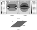
- the magnetic sensor 300 set forth in this application further includes a shielding assembly 330.
- the shielding assembly 330 is generally disposed on a surface of a side that is of the TMR element 320 and that is away from the PCB 310. Therefore, an external magnetic field is shielded and does not affect the detection result of the TMR element 320.
- the shielding assembly 330 is generally of a comb structure. An area of the comb structure is greater than an area of the surface of the side that is of the TMR element 320 and that is away from the PCB 310. In this way, the shielding assembly 330 can effectively shield the external magnetic field, and the external magnetic field does not affect the detection result of the TMR element 320.
- a shielding body with a complete structure eddy current effect is generated in the shielding body, and a surrounding magnetic field is severely distorted. This affects the detection result of the TMR element 320.
- a shielding body with the comb structure is used. In the comb structure, a gap exists between teeth that play a shielding function. Therefore, a path of the eddy current of the shielding body in a high-frequency magnetic field may be cut off. In this way, generation of eddy current effect in the shielding body is suppressed. In this way, a surrounding magnetic field is not distorted or is slightly distorted. This slightly affects the detection result of the TMR element 320.
- a shorter side length of the teeth and a shorter distance between the teeth indicate better suppression of the generation of eddy current effect in the shielding assembly 330, and small impact on the detection result of the TMR element 320.
- the shielding assembly 330 is not limited to the structure shown in FIG. 9 , and may be of another shape, for example, a semicircle shape.
- the shielding assembly 330 may cover the TMR element 320.
- the shielding assembly 330 may be of another shape. This is not limited in this application.
- An embodiment of this application further provides an electronic device.
- the electronic device includes at least one magnetic sensor recited in FIG. 3 to FIG. 9 and the corresponding claimed solutions. Because the electronic device includes the magnetic sensor, the electronic device has all or at least some advantages of the magnetic sensor.
- the electronic device may be an electric vehicle, a computer, or the like.
Landscapes
- Physics & Mathematics (AREA)
- General Physics & Mathematics (AREA)
- Condensed Matter Physics & Semiconductors (AREA)
- Measuring Magnetic Variables (AREA)
Applications Claiming Priority (2)
| Application Number | Priority Date | Filing Date | Title |
|---|---|---|---|
| CN202111360274.8A CN114252814A (zh) | 2021-11-17 | 2021-11-17 | 一种磁传感器和电子设备 |
| PCT/CN2022/103840 WO2023087740A1 (zh) | 2021-11-17 | 2022-07-05 | 一种磁传感器和电子设备 |
Publications (2)
| Publication Number | Publication Date |
|---|---|
| EP4407333A1 true EP4407333A1 (de) | 2024-07-31 |
| EP4407333A4 EP4407333A4 (de) | 2025-01-08 |
Family
ID=80790958
Family Applications (1)
| Application Number | Title | Priority Date | Filing Date |
|---|---|---|---|
| EP22894283.5A Withdrawn EP4407333A4 (de) | 2021-11-17 | 2022-07-05 | Magnetsensor und elektronische vorrichtung |
Country Status (4)
| Country | Link |
|---|---|
| US (1) | US20240295586A1 (de) |
| EP (1) | EP4407333A4 (de) |
| CN (1) | CN114252814A (de) |
| WO (1) | WO2023087740A1 (de) |
Families Citing this family (3)
| Publication number | Priority date | Publication date | Assignee | Title |
|---|---|---|---|---|
| CN114252814A (zh) * | 2021-11-17 | 2022-03-29 | 华为数字能源技术有限公司 | 一种磁传感器和电子设备 |
| US12510612B2 (en) * | 2023-11-29 | 2025-12-30 | Globalfoundries Singapore Pte. Ltd. | Current sensor for printed circuit board |
| CN120928028B (zh) * | 2025-10-11 | 2025-12-05 | 中国科学院合肥物质科学研究院 | 基于隧道磁电阻复合校正的霍尔电流传感器 |
Family Cites Families (11)
| Publication number | Priority date | Publication date | Assignee | Title |
|---|---|---|---|---|
| JP2002082136A (ja) * | 2000-06-23 | 2002-03-22 | Yazaki Corp | 電流センサ |
| TWI365989B (en) * | 2003-12-23 | 2012-06-11 | Eliposki Remote Ltd L L C | Semiconductor device and method for manufacturing the same |
| CN101788596A (zh) * | 2010-01-29 | 2010-07-28 | 王建国 | Tmr电流传感器 |
| JP6007479B2 (ja) * | 2011-11-14 | 2016-10-12 | 株式会社リコー | 電流センサ |
| JP5849654B2 (ja) * | 2011-11-30 | 2016-02-03 | 株式会社リコー | 電流センサ |
| US9417297B2 (en) * | 2012-02-16 | 2016-08-16 | Honeywell International Inc. | Tunneling magneto-resistive device with set/reset and offset straps |
| CN202903856U (zh) * | 2012-06-27 | 2013-04-24 | 浙江江森汽车零部件有限公司 | 一种tmr电流传感器 |
| JP6463560B2 (ja) * | 2017-01-25 | 2019-02-06 | 三菱電機株式会社 | 筐体及び磁気センサ装置 |
| EP3508863B1 (de) * | 2018-01-05 | 2023-06-07 | Melexis Technologies SA | Offsetstromsensorstruktur |
| CN112834805A (zh) * | 2021-01-04 | 2021-05-25 | 中国电力科学研究院有限公司 | 具有位置误差校准功能的隧穿磁阻电流传感器及校准方法 |
| CN114252814A (zh) * | 2021-11-17 | 2022-03-29 | 华为数字能源技术有限公司 | 一种磁传感器和电子设备 |
-
2021
- 2021-11-17 CN CN202111360274.8A patent/CN114252814A/zh active Pending
-
2022
- 2022-07-05 EP EP22894283.5A patent/EP4407333A4/de not_active Withdrawn
- 2022-07-05 WO PCT/CN2022/103840 patent/WO2023087740A1/zh not_active Ceased
-
2024
- 2024-05-13 US US18/662,985 patent/US20240295586A1/en not_active Abandoned
Also Published As
| Publication number | Publication date |
|---|---|
| US20240295586A1 (en) | 2024-09-05 |
| WO2023087740A1 (zh) | 2023-05-25 |
| EP4407333A4 (de) | 2025-01-08 |
| CN114252814A (zh) | 2022-03-29 |
Similar Documents
| Publication | Publication Date | Title |
|---|---|---|
| US20240295586A1 (en) | Magnetic sensor and electronic device | |
| EP2174152B1 (de) | Stromsensor mit zwischenangeordneter schicht für magnetische permeabilität | |
| US20230084942A1 (en) | Offset current sensor structure | |
| US8593134B2 (en) | Current sensor | |
| US7106046B2 (en) | Current measuring method and current measuring device | |
| US8754642B2 (en) | Magnetic balance type current sensor | |
| US7642768B1 (en) | Current sensor having field screening arrangement including electrical conductors sandwiching magnetic permeability layer | |
| JP5866583B2 (ja) | 電流センサ | |
| US20170307664A1 (en) | Sensors, systems and methods for residual current detection | |
| US20050140355A1 (en) | Eddy-current sensor for nondestructive testing | |
| US20100141251A1 (en) | Magnetic detection device | |
| JP2021135196A (ja) | 磁気センサ及び磁気検出方法 | |
| US20140015524A1 (en) | Integrated interconnect and magnetic-field detector for current sensing | |
| US8395383B2 (en) | Current sensor including magnetic detecting element | |
| US20240175948A1 (en) | Current Detection Apparatus and Electronic Device | |
| US12320869B2 (en) | Magnetic sensor and current sensor including magneto-resistance element | |
| CN223624299U (zh) | 分流器、新能源汽车及其储能设备 | |
| US20260072059A1 (en) | Sensor devices and associated production methods | |
| US20250180608A1 (en) | Magnetic sensor and current sensor | |
| JP2014098634A (ja) | 電流センサ | |
| JP2023179994A (ja) | 電子部品ユニット |
Legal Events
| Date | Code | Title | Description |
|---|---|---|---|
| STAA | Information on the status of an ep patent application or granted ep patent |
Free format text: STATUS: THE INTERNATIONAL PUBLICATION HAS BEEN MADE |
|
| PUAI | Public reference made under article 153(3) epc to a published international application that has entered the european phase |
Free format text: ORIGINAL CODE: 0009012 |
|
| STAA | Information on the status of an ep patent application or granted ep patent |
Free format text: STATUS: REQUEST FOR EXAMINATION WAS MADE |
|
| 17P | Request for examination filed |
Effective date: 20240418 |
|
| AK | Designated contracting states |
Kind code of ref document: A1 Designated state(s): AL AT BE BG CH CY CZ DE DK EE ES FI FR GB GR HR HU IE IS IT LI LT LU LV MC MK MT NL NO PL PT RO RS SE SI SK SM TR |
|
| REG | Reference to a national code |
Ref country code: DE Ref legal event code: R079 Free format text: PREVIOUS MAIN CLASS: G01R0033020000 Ipc: G01R0033090000 |
|
| A4 | Supplementary search report drawn up and despatched |
Effective date: 20241209 |
|
| RIC1 | Information provided on ipc code assigned before grant |
Ipc: G01R 15/20 20060101ALI20241203BHEP Ipc: G01R 33/09 20060101AFI20241203BHEP |
|
| DAV | Request for validation of the european patent (deleted) | ||
| DAX | Request for extension of the european patent (deleted) | ||
| STAA | Information on the status of an ep patent application or granted ep patent |
Free format text: STATUS: THE APPLICATION IS DEEMED TO BE WITHDRAWN |
|
| 18D | Application deemed to be withdrawn |
Effective date: 20250708 |