EP4403891A1 - Spektrometrievorrichtung - Google Patents
Spektrometrievorrichtung Download PDFInfo
- Publication number
- EP4403891A1 EP4403891A1 EP22869815.5A EP22869815A EP4403891A1 EP 4403891 A1 EP4403891 A1 EP 4403891A1 EP 22869815 A EP22869815 A EP 22869815A EP 4403891 A1 EP4403891 A1 EP 4403891A1
- Authority
- EP
- European Patent Office
- Prior art keywords
- light
- optical system
- spectrometry device
- object light
- face
- Prior art date
- Legal status (The legal status is an assumption and is not a legal conclusion. Google has not performed a legal analysis and makes no representation as to the accuracy of the status listed.)
- Pending
Links
- 238000004611 spectroscopical analysis Methods 0.000 title claims abstract description 79
- 230000003287 optical effect Effects 0.000 claims abstract description 85
- 229910052710 silicon Inorganic materials 0.000 claims abstract description 52
- 239000010703 silicon Substances 0.000 claims abstract description 52
- 238000003384 imaging method Methods 0.000 claims abstract description 46
- 239000000463 material Substances 0.000 claims abstract description 44
- 238000005259 measurement Methods 0.000 claims abstract description 29
- 238000001816 cooling Methods 0.000 claims description 47
- PCHJSUWPFVWCPO-UHFFFAOYSA-N gold Chemical compound [Au] PCHJSUWPFVWCPO-UHFFFAOYSA-N 0.000 claims description 20
- 229910052737 gold Inorganic materials 0.000 claims description 20
- 239000010931 gold Substances 0.000 claims description 20
- 238000012545 processing Methods 0.000 claims description 18
- 230000003014 reinforcing effect Effects 0.000 claims description 8
- 230000008878 coupling Effects 0.000 claims description 2
- 238000010168 coupling process Methods 0.000 claims description 2
- 238000005859 coupling reaction Methods 0.000 claims description 2
- XUIMIQQOPSSXEZ-UHFFFAOYSA-N Silicon Chemical compound [Si] XUIMIQQOPSSXEZ-UHFFFAOYSA-N 0.000 description 44
- 230000005855 radiation Effects 0.000 description 43
- 230000005540 biological transmission Effects 0.000 description 21
- 239000013078 crystal Substances 0.000 description 12
- 230000008859 change Effects 0.000 description 10
- 229910052751 metal Inorganic materials 0.000 description 9
- 239000002184 metal Substances 0.000 description 9
- 230000003595 spectral effect Effects 0.000 description 8
- 238000002474 experimental method Methods 0.000 description 7
- 230000007246 mechanism Effects 0.000 description 7
- 239000003507 refrigerant Substances 0.000 description 7
- 238000001228 spectrum Methods 0.000 description 7
- VYPSYNLAJGMNEJ-UHFFFAOYSA-N Silicium dioxide Chemical compound O=[Si]=O VYPSYNLAJGMNEJ-UHFFFAOYSA-N 0.000 description 6
- 238000000151 deposition Methods 0.000 description 6
- 230000001965 increasing effect Effects 0.000 description 6
- 239000012530 fluid Substances 0.000 description 5
- 230000002093 peripheral effect Effects 0.000 description 5
- 230000014509 gene expression Effects 0.000 description 4
- 238000000034 method Methods 0.000 description 4
- 230000008021 deposition Effects 0.000 description 3
- 238000001514 detection method Methods 0.000 description 3
- 230000000694 effects Effects 0.000 description 3
- 238000005530 etching Methods 0.000 description 3
- 229910001220 stainless steel Inorganic materials 0.000 description 3
- 239000010935 stainless steel Substances 0.000 description 3
- 238000012360 testing method Methods 0.000 description 3
- 229910052782 aluminium Inorganic materials 0.000 description 2
- XAGFODPZIPBFFR-UHFFFAOYSA-N aluminium Chemical compound [Al] XAGFODPZIPBFFR-UHFFFAOYSA-N 0.000 description 2
- HVYWMOMLDIMFJA-DPAQBDIFSA-N cholesterol Chemical compound C1C=C2C[C@@H](O)CC[C@]2(C)[C@@H]2[C@@H]1[C@@H]1CC[C@H]([C@H](C)CCCC(C)C)[C@@]1(C)CC2 HVYWMOMLDIMFJA-DPAQBDIFSA-N 0.000 description 2
- 230000007423 decrease Effects 0.000 description 2
- 239000003574 free electron Substances 0.000 description 2
- 238000010438 heat treatment Methods 0.000 description 2
- 150000002894 organic compounds Chemical class 0.000 description 2
- 230000002787 reinforcement Effects 0.000 description 2
- 239000000126 substance Substances 0.000 description 2
- WQZGKKKJIJFFOK-GASJEMHNSA-N Glucose Natural products OC[C@H]1OC(O)[C@H](O)[C@@H](O)[C@@H]1O WQZGKKKJIJFFOK-GASJEMHNSA-N 0.000 description 1
- WQZGKKKJIJFFOK-VFUOTHLCSA-N beta-D-glucose Chemical compound OC[C@H]1O[C@@H](O)[C@H](O)[C@@H](O)[C@@H]1O WQZGKKKJIJFFOK-VFUOTHLCSA-N 0.000 description 1
- 239000008280 blood Substances 0.000 description 1
- 210000004369 blood Anatomy 0.000 description 1
- 235000012000 cholesterol Nutrition 0.000 description 1
- 230000001419 dependent effect Effects 0.000 description 1
- 230000002542 deteriorative effect Effects 0.000 description 1
- 230000002708 enhancing effect Effects 0.000 description 1
- 239000008103 glucose Substances 0.000 description 1
- 238000012986 modification Methods 0.000 description 1
- 230000004048 modification Effects 0.000 description 1
- 230000035945 sensitivity Effects 0.000 description 1
Images


Classifications
-
- G—PHYSICS
- G01—MEASURING; TESTING
- G01N—INVESTIGATING OR ANALYSING MATERIALS BY DETERMINING THEIR CHEMICAL OR PHYSICAL PROPERTIES
- G01N21/00—Investigating or analysing materials by the use of optical means, i.e. using sub-millimetre waves, infrared, visible or ultraviolet light
- G01N21/17—Systems in which incident light is modified in accordance with the properties of the material investigated
- G01N21/25—Colour; Spectral properties, i.e. comparison of effect of material on the light at two or more different wavelengths or wavelength bands
- G01N21/31—Investigating relative effect of material at wavelengths characteristic of specific elements or molecules, e.g. atomic absorption spectrometry
- G01N21/35—Investigating relative effect of material at wavelengths characteristic of specific elements or molecules, e.g. atomic absorption spectrometry using infrared light
-
- G—PHYSICS
- G01—MEASURING; TESTING
- G01J—MEASUREMENT OF INTENSITY, VELOCITY, SPECTRAL CONTENT, POLARISATION, PHASE OR PULSE CHARACTERISTICS OF INFRARED, VISIBLE OR ULTRAVIOLET LIGHT; COLORIMETRY; RADIATION PYROMETRY
- G01J3/00—Spectrometry; Spectrophotometry; Monochromators; Measuring colours
- G01J3/28—Investigating the spectrum
- G01J3/45—Interferometric spectrometry
- G01J3/453—Interferometric spectrometry by correlation of the amplitudes
-
- G—PHYSICS
- G01—MEASURING; TESTING
- G01J—MEASUREMENT OF INTENSITY, VELOCITY, SPECTRAL CONTENT, POLARISATION, PHASE OR PULSE CHARACTERISTICS OF INFRARED, VISIBLE OR ULTRAVIOLET LIGHT; COLORIMETRY; RADIATION PYROMETRY
- G01J3/00—Spectrometry; Spectrophotometry; Monochromators; Measuring colours
- G01J3/02—Details
- G01J3/0205—Optical elements not provided otherwise, e.g. optical manifolds, diffusers, windows
- G01J3/0208—Optical elements not provided otherwise, e.g. optical manifolds, diffusers, windows using focussing or collimating elements, e.g. lenses or mirrors; performing aberration correction
-
- G—PHYSICS
- G01—MEASURING; TESTING
- G01J—MEASUREMENT OF INTENSITY, VELOCITY, SPECTRAL CONTENT, POLARISATION, PHASE OR PULSE CHARACTERISTICS OF INFRARED, VISIBLE OR ULTRAVIOLET LIGHT; COLORIMETRY; RADIATION PYROMETRY
- G01J3/00—Spectrometry; Spectrophotometry; Monochromators; Measuring colours
- G01J3/02—Details
- G01J3/0205—Optical elements not provided otherwise, e.g. optical manifolds, diffusers, windows
- G01J3/021—Optical elements not provided otherwise, e.g. optical manifolds, diffusers, windows using plane or convex mirrors, parallel phase plates, or particular reflectors
-
- G—PHYSICS
- G01—MEASURING; TESTING
- G01J—MEASUREMENT OF INTENSITY, VELOCITY, SPECTRAL CONTENT, POLARISATION, PHASE OR PULSE CHARACTERISTICS OF INFRARED, VISIBLE OR ULTRAVIOLET LIGHT; COLORIMETRY; RADIATION PYROMETRY
- G01J3/00—Spectrometry; Spectrophotometry; Monochromators; Measuring colours
- G01J3/02—Details
- G01J3/0205—Optical elements not provided otherwise, e.g. optical manifolds, diffusers, windows
- G01J3/0229—Optical elements not provided otherwise, e.g. optical manifolds, diffusers, windows using masks, aperture plates, spatial light modulators or spatial filters, e.g. reflective filters
-
- G—PHYSICS
- G01—MEASURING; TESTING
- G01J—MEASUREMENT OF INTENSITY, VELOCITY, SPECTRAL CONTENT, POLARISATION, PHASE OR PULSE CHARACTERISTICS OF INFRARED, VISIBLE OR ULTRAVIOLET LIGHT; COLORIMETRY; RADIATION PYROMETRY
- G01J3/00—Spectrometry; Spectrophotometry; Monochromators; Measuring colours
- G01J3/02—Details
- G01J3/0262—Constructional arrangements for removing stray light
-
- G—PHYSICS
- G01—MEASURING; TESTING
- G01J—MEASUREMENT OF INTENSITY, VELOCITY, SPECTRAL CONTENT, POLARISATION, PHASE OR PULSE CHARACTERISTICS OF INFRARED, VISIBLE OR ULTRAVIOLET LIGHT; COLORIMETRY; RADIATION PYROMETRY
- G01J3/00—Spectrometry; Spectrophotometry; Monochromators; Measuring colours
- G01J3/02—Details
- G01J3/0286—Constructional arrangements for compensating for fluctuations caused by temperature, humidity or pressure, or using cooling or temperature stabilization of parts of the device; Controlling the atmosphere inside a spectrometer, e.g. vacuum
-
- G—PHYSICS
- G01—MEASURING; TESTING
- G01J—MEASUREMENT OF INTENSITY, VELOCITY, SPECTRAL CONTENT, POLARISATION, PHASE OR PULSE CHARACTERISTICS OF INFRARED, VISIBLE OR ULTRAVIOLET LIGHT; COLORIMETRY; RADIATION PYROMETRY
- G01J3/00—Spectrometry; Spectrophotometry; Monochromators; Measuring colours
- G01J3/02—Details
- G01J3/0291—Housings; Spectrometer accessories; Spatial arrangement of elements, e.g. folded path arrangements
-
- G—PHYSICS
- G01—MEASURING; TESTING
- G01J—MEASUREMENT OF INTENSITY, VELOCITY, SPECTRAL CONTENT, POLARISATION, PHASE OR PULSE CHARACTERISTICS OF INFRARED, VISIBLE OR ULTRAVIOLET LIGHT; COLORIMETRY; RADIATION PYROMETRY
- G01J3/00—Spectrometry; Spectrophotometry; Monochromators; Measuring colours
- G01J3/12—Generating the spectrum; Monochromators
- G01J3/18—Generating the spectrum; Monochromators using diffraction elements, e.g. grating
-
- G—PHYSICS
- G01—MEASURING; TESTING
- G01J—MEASUREMENT OF INTENSITY, VELOCITY, SPECTRAL CONTENT, POLARISATION, PHASE OR PULSE CHARACTERISTICS OF INFRARED, VISIBLE OR ULTRAVIOLET LIGHT; COLORIMETRY; RADIATION PYROMETRY
- G01J3/00—Spectrometry; Spectrophotometry; Monochromators; Measuring colours
- G01J3/28—Investigating the spectrum
- G01J3/2803—Investigating the spectrum using photoelectric array detector
-
- G—PHYSICS
- G01—MEASURING; TESTING
- G01J—MEASUREMENT OF INTENSITY, VELOCITY, SPECTRAL CONTENT, POLARISATION, PHASE OR PULSE CHARACTERISTICS OF INFRARED, VISIBLE OR ULTRAVIOLET LIGHT; COLORIMETRY; RADIATION PYROMETRY
- G01J3/00—Spectrometry; Spectrophotometry; Monochromators; Measuring colours
- G01J3/28—Investigating the spectrum
- G01J3/44—Raman spectrometry; Scattering spectrometry ; Fluorescence spectrometry
-
- G—PHYSICS
- G01—MEASURING; TESTING
- G01J—MEASUREMENT OF INTENSITY, VELOCITY, SPECTRAL CONTENT, POLARISATION, PHASE OR PULSE CHARACTERISTICS OF INFRARED, VISIBLE OR ULTRAVIOLET LIGHT; COLORIMETRY; RADIATION PYROMETRY
- G01J3/00—Spectrometry; Spectrophotometry; Monochromators; Measuring colours
- G01J3/28—Investigating the spectrum
- G01J3/45—Interferometric spectrometry
- G01J3/453—Interferometric spectrometry by correlation of the amplitudes
- G01J3/4531—Devices without moving parts
-
- G—PHYSICS
- G01—MEASURING; TESTING
- G01N—INVESTIGATING OR ANALYSING MATERIALS BY DETERMINING THEIR CHEMICAL OR PHYSICAL PROPERTIES
- G01N2201/00—Features of devices classified in G01N21/00
- G01N2201/06—Illumination; Optics
- G01N2201/063—Illuminating optical parts
- G01N2201/0633—Directed, collimated illumination
-
- G—PHYSICS
- G01—MEASURING; TESTING
- G01N—INVESTIGATING OR ANALYSING MATERIALS BY DETERMINING THEIR CHEMICAL OR PHYSICAL PROPERTIES
- G01N2201/00—Features of devices classified in G01N21/00
- G01N2201/06—Illumination; Optics
- G01N2201/063—Illuminating optical parts
- G01N2201/0635—Structured illumination, e.g. with grating
Definitions
- the present invention relates to a spectrometry device.
- Methods for measuring spectral characteristics of object light include a method in which object light is converted into a parallel light beam by an objective lens, guided to an optical path length differentiating optical system, and divided into two light beams, then an optical path difference is provided between the two light beams, interference light is obtained by causing the two light beams to interfere with each other, and spectral characteristics are obtained from an intensity change of the interference light with respect to the optical path length difference between the two light beams.
- a system in which a fixed mirror and a movable mirror are disposed side by side is used as an optical path length differentiating optical system.
- Patent Literature 2 proposes a method for measuring a change in intensity of interference light at once without using a moving mechanism of a movable mirror.
- an optical path length differentiating optical system which includes two flat mirrors (a reference mirror and an inclined mirror) disposed side by side and having different inclinations of reflection faces.
- the reference mirror and the inclined mirror are disposed side by side along an axis perpendicular to a plane including the traveling direction of object light incident on the reference mirror and the traveling direction of the object light reflected by the reference mirror, and the reflection face of the inclined mirror is rotated about the axis.
- the object light is converted to parallel light beams, and the light beams are reflected by the respective reflection faces of the reference mirror and the inclined mirror.
- the light beams are each condensed in a direction of the axis by an imaging optical system, and focused on the same line segment perpendicular to the axis.
- an interference image is formed by the light (reference reflected light) reflected by the reference mirror and the light (inclined reflected light) reflected by the inclined mirror. Since the reflection face of the reference mirror and the reflection face of the inclined mirror make an angle, a continuous optical path length difference according to the angle formed by both reflection faces is generated between the reference reflected light and the inclined reflected light. Therefore, an interferogram representing the intensity change of the interference light with respect to the optical path length difference between the two light beams can be obtained by detecting the light intensity change of the interference image along the imaging straight line. By Fourier-transforming the interferogram, the spectral characteristics of the object light can be obtained
- Patent Literature 3 to 5 propose using an amplitude-type diffraction grating for enhancing the definition of an interference image.
- a plane optically conjugate with a surface (object face) of a sample is formed by using a conjugate plane imaging optical system, and an amplitude-type diffraction grating is disposed on this optically conjugate plane.
- the amplitude-type diffraction grating is formed by periodically providing openings in a light shielding plate made from, for example, a single crystal of silicon. Providing the plurality of openings in a direction parallel to the imaging line segment, it is expected to enhance the definition of the interference image.
- Patent Literature 4 discloses that providing a plurality of openings at a predetermined period in a direction perpendicular to the imaging line segment enhances the definition of the interference image. Furthermore, Patent Literature 5 describes that using an amplitude-type diffraction grating provided with openings as in Patent Literature 4 enhances the definition of the interference image in a spectrometry device using a fixed mirror and a movable mirror as described in Patent Literature 1.
- a problem to be solved by the present invention is to enhance the definition of an interference image of object light which is medium infrared rays emitted from a sample.
- a spectrometry device made to solve the above problems includes:
- the amplitude-type diffraction grating may be entirely made of a material having a light shielding rate higher than that of silicon in the wavelength band of the object light, or only a light incident face or a light emission face may be formed of a material having a light shielding rate higher than that of silicon in the wavelength band. In addition, both the light incident face and the light emission face may be formed of a material having a light shielding rate higher than that of silicon.
- the spectrometry device uses an amplitude-type diffraction grating in which a light incident face on which the object light is incident or a light emission face from which the object light is emitted is formed by a light-shielding member made of a material having an absorptivity or a reflectance higher than that of silicon in the wavelength band of the object light and provided with a plurality of openings, the amplitude-type diffraction grating being disposed on the conjugate surface.
- the material having an absorptivity higher than that of silicon include quartz glass and various organic compounds.
- Examples of the material having a reflectance higher than that of silicon include aluminum and gold.
- the material is not limited to pure metal, and it is also possible to use any kind of metal having free electrons such as stainless steel (SUS).
- the spectrometry device may have a configuration in which the light-shielding member includes a reflection member disposed on a side of the light incident face and made of the material having a reflectance higher than that of silicon in the wavelength band of the object light, and an absorbing member disposed on a side of the light emission face and made of a material having an absorptivity than that of silicon in a wavelength band of the object light.
- the object light incident on the light-shielding portion can be absorbed by using a light-shielding member (absorbing member) made from a quartz glass having a thickness of about 0.1 mm in general.
- a light-shielding member absorbing member
- the intensity of the object light is high, it may be difficult for the light-shielding member made only from a quartz glass to completely absorb the object light incident on the light-shielding portion.
- the reflection member is disposed on the side of the light incident face of the absorbing member, and the object light is reflected by the reflection member, so that the object light transmitted through the light-shielding portion of the light-shielding member can be further reduced.
- the spectrometry device may adopt a configuration that further includes a reinforcing member reinforcing the light-shielding member.
- the object light incident on the light-shielding portion can be absorbed by using a light-shielding member made from a quartz glass having a thickness of about 0.1 mm in general.
- a thin member has insufficient strength, so that the member is easily damaged and is difficult to handle.
- the spectrometry device described above includes the reinforcing member, and can thereby have sufficient strength.
- the reinforcing member can adopt any shape as long as the strength of the light-shielding member can be increased.
- the reinforcing member may be provided with a plurality of openings similarly to the light-shielding member, or may be a frame-shaped member reinforcing the peripheral portion of the light-shielding member.
- antireflection processing various types of antireflection processing can be used, for example, one with which a large number of structures each having a size equal to or less than the wavelength of the object light (subwavelength structure) are provided, one with which the light emission face is sandblasted to be a rough surface, one with which the light emission face is given an inclination to suppress direct reflection by the light emission face, and the like.
- Mid-infrared-ray measuring photodetectors include a thermal-type photodetector and a quantum-type photodetector.
- the thermal-type photodetector makes target mid-infrared rays enter a substance having a temperature-dependent electric resistance, measures the electric resistance value of the substance, and thereby measures the intensity of mid-infrared rays.
- the quantum-type photodetector photoelectrically converts incident mid-infrared rays to generate electric signals and detects the electric signals.
- the quantum-type photodetector has higher sensitivity than the thermal-type photodetector, but is generally expensive because the quantum-type photodetector is necessary to use a cooling mechanism for suppressing generation of thermal noise.
- a thermal-type photodetector is often used in order to suppress the cost of the device.
- incident mid-infrared rays are thermally coupled to a sensor to generate heat, and thus radiation light due to the heat is generated.
- the radiation light re-entering the photodetector after being reflected by the amplitude-type diffraction grating also becomes a factor of deteriorating the definition of an interference image.
- the light emission face is made of a material such as metal having a high reflectance as described above, the light emitted from the photodetector is directly reflected by the light emission face and enters the photodetector again.
- the spectrometry device described above uses an amplitude-type diffraction grating having the light emission face subjected to antireflection processing, so that the definition of interference light can be enhanced as compared with a conventional manner.
- the definition of an interference image of object light can be enhanced.
- Fig. 1 shows a schematic configuration of a spectrometry device 1 according to a first example.
- Fig. 2 is a plane view of the spectrometry device 1.
- the spectrometry device 1 includes an imaging lens 11, a multi-slit 13, an objective lens 15, a phase shifter 16, an imaging lens 17, and a two-dimensional detector 18 in the order closest to a sample S.
- a conjugate plane imaging optical system is configured between the sample S, the imaging lens 11, and the multi-slit 13.
- An imaging type two-dimensional Fourier spectroscopic optical system is configured between the multi-slit 13, the objective lens 15, the phase shifter 16, the imaging lens 17, and the two-dimensional detector 18.
- the spectrometry device 1 further includes an arithmetic operation unit configured to obtain an interferogram from a detection signal of the two-dimensional detector 18 and mathematically performs the Fourier-transform on the interferogram to obtain a spectral characteristic (spectrum) that is a relative intensity for each wavelength of the radiation light, and a control/processing unit 25 having functions of a processing unit, for example, imaging an arithmetic operation result of the arithmetic operation unit.
- an arithmetic operation unit configured to obtain an interferogram from a detection signal of the two-dimensional detector 18 and mathematically performs the Fourier-transform on the interferogram to obtain a spectral characteristic (spectrum) that is a relative intensity for each wavelength of the radiation light
- a control/processing unit 25 having functions of a processing unit, for example, imaging an arithmetic operation result of the arithmetic operation unit.
- the imaging lens 11 By the imaging lens 11, light (object light) emitted in various directions from each of a large number of measurement points disposed on the surface of the sample S is condensed on the position of the multi-slit 13.
- the imaging lens 11 forms a plane optically conjugate with the surface of the sample S at the position of the multi-slit 13.
- the imaging lens 11 corresponds to the conjugate plane imaging optical system in the present invention.
- Fig. 2 shows one of a large number of measurement points as a measurement point a1.
- the phase shifter 16 is installed to be inclined by about 45° with respect to the optical axis of the incident object light, and includes a fixed mirror unit 16a and a movable mirror unit 16b that are disposed vertically on an upper side and a lower side, respectively.
- the movable mirror unit 16b is moved in a direction indicated by an arrow by a driving mechanism (not shown).
- the fixed mirror unit 16a or the movable mirror unit 16b may be disposed on either the upper side or the lower side.
- the movable mirror unit 16b is disposed on the upper side
- the fixed mirror unit 16a is disposed on the lower side.
- the fixed mirror unit and the movable mirror unit can be disposed on the left and the right, respectively.
- the fixed mirror unit and the movable mirror unit are disposed in the vertical direction.
- the phase shifter 16 corresponds to the optical path length differentiating optical system in the present invention.
- the imaging lens 17 causes the object light reflected by the fixed mirror unit 16a and the object light reflected by the movable mirror unit 16b to interfere with each other and converges the interfered object light on a light-receiving face of the two-dimensional detector 18.
- the imaging lens 17 corresponds to the interference optical system in the present invention.
- the multi-slit 13 corresponds to the amplitude-type diffraction grating in the present invention.
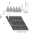
- the multi-slit 13 is formed by etching a single crystal of silicon to form openings 132, forming a subwavelength structure (SWC) in which convex portions 133 each having a quadrangular pyramidal shape are periodically disposed on the single crystal of silicon with a period equal to or less than the wavelength of object light emitted from the sample S, and depositing gold on the surface of the SWC.
- SWC subwavelength structure
- the plurality of openings 132 each having a belt shape are periodically disposed in one direction (first axis direction) on a base member 131 having a rectangular plate shape and a light shielding property with respect to mid-infrared light to be measured.
- a cooling member 14 for cooling the multi-slit 13 is disposed.
- the cooling member 14 for example, a Peltier element or a member having a flow path in which a refrigerant fluid flows can be used.
- a length Wi of the opening 132 in the first axis direction and a period L 1 of the openings 132 adjacent to each other in the first axis direction are designed to satisfy the following expressions (1) and (2), respectively.
- W 1 P 1 ⁇ 2 / m + 1
- L 1 P 1 ⁇ 2 / m
- P 1 is an interval between pixels 181 of the two-dimensional detector 18 in the first axis direction
- m is an optical magnification of an optical system including the multi-slit 13, the objective lens 15, the phase shifter 16, the imaging lens 17, and the two-dimensional detector 18.
- the fixed mirror unit 16a and the movable mirror unit 16b are irradiated with the object light, but in a cross section containing the horizontal axis, either one of the fixed mirror unit 16a and the movable mirror unit 16b is irradiated with the object light. That is, the optical path length difference changes and the interference intensity changes with the movement of movable mirror unit 16b in a cross section containing the vertical axis, but there is no optical path length difference and no interference intensity change occurs in a cross section containing the horizontal axis. Therefore, in the first example, the multi-slit 13 having a combination of openings and light-shielding portions configured to eliminate phase cancellation between bright spots (measurement points) is disposed in the vertical axis direction (first axis direction).
- the two-dimensional detector 18 is a thermal-type photodetector.
- the thermal-type photodetector converts heat generated by thermally coupling incident mid-infrared rays and a sensor into electric signals and detects the electric signals.
- Specific examples of the thermal-type detector include a microbolometer array sensor.
- the light-receiving face is cooled by a cooling member 19 (not shown in Figs. 1 and 4 ).
- a cooling member 19 for example, a Peltier element or a member having a flow path in which a refrigerant fluid flows can be used.
- the processing unit 25 obtains an interferogram from the light intensity distribution of the interference image obtained by the two-dimensional detector 18 and Fourier-transforms the interferogram to obtain a spectrum of the measurement point.
- the imaging lens 11 by the imaging lens 11, the object light emitted from each of a large number of the measurement points located on the surface of the sample S is condensed on the position of the multi-slit 13.
- the object light having passed through the openings 132 of the multi-slit 13 is collimated by the objective lens 15 and incident on the fixed mirror unit 16a and the movable mirror unit 16b of the phase shifter 16.
- an optical path length difference is imparted between the object light reflected by the fixed mirror unit 16a and the object light reflected by the movable mirror unit 16b, and then an image is formed on the light-receiving face of the two-dimensional detector 18 by the imaging lens 17.
- Fig. 2 only the optical path of the object light emitted from one measurement point a1 on the surface of the sample S is shown in order to clearly illustrate the optical path of the object light, but actually, interference light is formed from the object light emitted from each of the plurality of measurement points a that are two-dimensionally distributed on the surface of the sample S, and is incident on each light receiving element two-dimensionally arrayed on the light-receiving face of the two-dimensional detector 18.
- the spectrometry device 1 according to the first example is particularly characterized by the configuration of the multi-slit 13 (configuration having a subwavelength structure that is formed on the surface facing the detector and on which gold is deposited), the cooling member 14 configured to cool the multi-slit 13, and the cooling member 19 configured to cool the light-receiving face of the two-dimensional detector 18.
- the spectrometry device 1 according to the first example includes all of these three configurations as a preferred specific mode of the present invention, but can adopt a configuration including only some of these three features.
- the present inventor conducted an experiment of measuring radiation light emitted from a black body at each temperature by heating or cooling the black body to a plurality of different temperatures at room temperature to check a change in luminance amplitude of the interference image.
- the magnitude of the luminance amplitude corresponds to the height of the center burst in an interferogram.
- a conventional spectrometry device a device having a configuration obtained by removing the above three features from the spectrometry device 1 according to the above-described example was used.
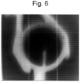
- Fig. 5 is a graph showing the result of the above experiment. As shown in this graph, in the conventional spectrometry device, the luminance amplitude of the interference light obtained when the black body was heated to about 35 °C close to room temperature was minimized. A gas cell filled with DME gas was disposed on the surface of a refrigerant, and a mid-infrared image of the surface of the refrigerant was captured. As shown in Fig. 6 , the luminance at the position of the light-shielding portion was higher than the luminance at the position of the opening. The results shown in Figs.
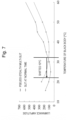
- Fig. 7 shows the result of the above experiment.
- the brightness is minimized when the temperature of the black body is raised to 35 °C
- the brightness is minimized when the temperature of the black body is 25 °C
- the temperature at which the luminance amplitude is minimized changes when the material constituting the surface of the slit facing the two-dimensional detector is changed.
- the configuration in which the gold deposition surface is disposed to face the two-dimensional detector should have less light incident on the two-dimensional detector, and the temperature at which the luminance amplitude is minimized should be lower.
- the temperature at which the luminance amplitude is minimized is actually higher when the gold deposited surface faces the two-dimensional detector side as described above.
- the reflectance of silicon is smaller than that of gold, and that a thermal-type detector is used as the two-dimensional detector, it is considered that another factor causing light to be emitted from the slit is that radiation light due to heat generated inside the two-dimensional detector is reflected by the light-shielding portion of the slit, and the radiation light is incident on the two-dimensional detector again.
- factors causing light to be emitted from the slit are the light radiated from the base member of the slit and the light emitted from the two-dimensional detector and reflected by the light-shielding portion of the slit.
- the spectrometry device 1 of the first example by using a material in which gold is deposited on the surface on the two-dimensional detector 18 side as the base member 131 of the multi-slit 13, the emissivity is reduced (the radiation light from the slit itself is suppressed) as compared with the base member made of a single crystal of silicon.
- the subwavelength structure (SWC) in which the convex portions 133 are disposed with a period equal to or less than the wavelength of the object light emitted from the sample S is produced by surface forming, so that the reflectance (reflection of the radiation light from the two-dimensional detector 18) is reduced.
- the cooling member 14 By cooling the multi-slit 13 by the cooling member 14, the radiation light of the multi-slit 13 itself is further suppressed. Furthermore, by cooling the light-receiving face of the two-dimensional detector 18 with the cooling member 19, radiation light due to heat generated inside the two-dimensional detector 18 is also suppressed.
- the above-described pseudo-stealth multi-slit it is possible to adopt a configuration in which the reflection of the radiation light from the two-dimensional detector 18 is reduced and the radiation light of the slit itself is suppressed by cooling the multi-slit 13 with the cooling member 14.
- a spectrometry device 100 of a second example is also used to obtain the optical spectrum of the mid-infrared light emitted from the sample to be analyzed.
- the interferogram of the object light emitted from each of the measurement points a1 distributed on the surface of the sample S in the first axis direction is obtained.
- Fig. 8 shows a schematic configuration of the spectrometry device 100 according to the second example.
- Figs. 9 and 10 are a plane view and a side view of the spectrometry device 100.
- the spectrometry device 100 includes an imaging lens 111, a two-dimensional slit 113, an objective lens 115, a phase shifter 116, a cylindrical lens 117, and a two-dimensional detector 118 in the order closest to the sample S.
- the spectrometry device 100 includes an arithmetic operation unit configured to obtain an interferogram from a detection signal of the two-dimensional detector 118 and mathematically performs the Fourier-transform on the interferogram to obtain a spectral characteristic (spectrum) that is a relative intensity for each wavelength of the radiation light, and a control/processing unit 125 having functions of a processing unit, for example, imaging an arithmetic operation result of the arithmetic operation unit.
- arithmetic operation unit configured to obtain an interferogram from a detection signal of the two-dimensional detector 118 and mathematically performs the Fourier-transform on the interferogram to obtain a spectral characteristic (spectrum) that is a relative intensity for each wavelength of the radiation light
- a control/processing unit 125 having functions of a processing unit, for example, imaging an arithmetic operation result of the arithmetic operation unit.
- the imaging lens 111 By the imaging lens 111, the object light emitted in various directions from each of the measurement points disposed on the surface of the sample S is condensed on the position of the two-dimensional slit 113.
- the imaging lens 111 forms a plane optically conjugate with the surface of the sample S at the position of the two-dimensional slit 113.
- the imaging lens 111 corresponds to the conjugate plane imaging optical system in the present invention.
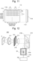
- the two-dimensional slit 113 corresponds to the amplitude-type diffraction grating in the present invention. As shown in the front view and the side view in Fig. 11 , in the two-dimensional slit 113, a plurality of openings 1132 are periodically disposed in two directions (first axis direction and second axis direction) orthogonal to each other on a base member 1131 having a rectangular plate shape and a light shielding property with respect to mid-infrared light to be measured.
- a length Wi of the opening 1132 in the first axis direction and a period L 1 of the openings 1132 adjacent to each other in the first axis direction are designed to satisfy the following expressions (1) and (2), respectively.
- W 1 P 1 ⁇ 2 / m + 1
- L 1 P 1 ⁇ 2 / m
- P 1 is an interval between pixels of the two-dimensional detector 118 in the first axis direction
- m is an optical magnification of an optical system including the two-dimensional slit 113, the objective lens 115, the phase shifter 116, the cylindrical lens 117, and the two-dimensional detector 118.
- a length W 2 of the opening 1132 in the second axis direction and a period L 2 of the openings 1132 adjacent to each other in the second axis direction are designed to satisfy the following expressions (3) and (4).
- W 2 ⁇ C ⁇ f / 2 ⁇ ⁇ ⁇ h ⁇ P 2
- L 2 2 ⁇ ⁇ C ⁇ f / 2 ⁇ ⁇ ⁇ h ⁇ P 2
- ⁇ C is a wavelength included in object light
- f is a focal length of the objective lens 115
- ⁇ is a difference between optical path lengths of a first light beam of the object light having passed through a first transmission portion 116a (described later) and a second light beam of the object light having passed through a second transmission portion 116b (described later), which are incident on pixels adjacent to each other in the second axis direction in the two-dimensional detector 118
- h is a distance from the phase shifter 116 to a light-receiving face of the two-dimensional detector 118.
- the two-dimensional slit 113 in the second example is also formed by etching a single crystal of silicon to form the openings 1132, forming a subwavelength structure (SWC) in which convex portions 1133 each having a quadrangular pyramidal shape are periodically disposed on the single crystal of silicon with a period equal to or less than the wavelength of object light emitted from the sample S as shown in Fig. 11 , and depositing gold on the surface of the SWC.
- the surface on the side on which the convex portions 1133 are formed is disposed on the two-dimensional detector 118 side.
- a cooling member 114 (not shown in Figs.
- cooling member 114 for example, a Peltier element similar to the first example or a member having a flow path in which a refrigerant fluid flows can be used.
- the phase shifter 116 includes the first transmission portion 116a and the second transmission portion 116b that are made of a material having transparency to mid-infrared light and are disposed side by side in the second axis direction.
- the first transmission portion 116a is a rectangular plate-like optical member having a constant thickness in which a light incident face and a light emission face are parallel.
- the second transmission portion 116b is a trapezoidal optical member in plane view the thickness of which continuously changes along the second axis.
- the second transmission portion 116b has: a light incident face inclined with respect to the light incident face of the first transmission portion 116a; and a light emission face on the same plane as the light emission face of the first transmission portion 116a.
- the phase shifter 116 corresponds to the optical path length differentiating optical system in the present invention.
- the cylindrical lens 117 is a semicircular columnar member made of a material having transparency to mid-infrared light.
- the cylindrical lens 117 is disposed so that the convex side faces the phase shifter 116 side, the flat surface faces the two-dimensional detector 118 side, and the semicircular cross section is disposed orthogonal to the second axis.
- the cylindrical lens 117 corresponds to the interference optical system in the present invention.
- a thermal photodetector is used as the two-dimensional detector 118.
- the light-receiving face is cooled by a cooling member 119 (not shown in Figs. 9 and 10 ).
- a cooling member 119 for example, a Peltier element similar to the first example or a member having a flow path in which a refrigerant fluid flows can be used.
- the control/processing unit 125 obtains an interferogram from the light intensity distribution of the interference image obtained by the two-dimensional detector 118 and Fourier-transforms the interferogram to obtain a spectrum of the measurement point.
- the imaging lens 111 by the imaging lens 111, the object light that is mid-infrared light emitted from one of the measurement points a1 located on the surface of the sample S is condensed on the position of the two-dimensional slit 113.
- the object light having passed through the openings 1132 of the two-dimensional slit 113 is collimated by the objective lens 115 and incident on the first transmission portion 116a and the second transmission portion 116b of the phase shifter 116.
- a continuous optical path length difference is provided along the second axis between the object light (first light beam) having passed through the first transmission portion 116a and the object light (second light beam) having passed through the second transmission portion 116b.
- the object light having passed through the first transmission portion 116a and the object light having passed through the second transmission portion 116b are condensed in the first axis direction by the cylindrical lens 117, and formed as a linear interference image along the second axis on the light-receiving face of the two-dimensional detector 118.
- Figs. 8 to 10 only the optical path of the object light emitted from one measurement point a1 on the surface of the sample S is shown in order to clearly illustrate the optical path of the object light, but actually, interference images are formed side by side along the first axis direction from the object light emitted from each of the plurality of measurement points adjacent to the measurement point a1 in the first axis direction, on the light-receiving face of the two-dimensional detector 118. Therefore, in the spectrometry device 100 according to the second example, the interference images formed by the object light emitted from each of the plurality of measurement points adjacent to each other along the first axis on the surface of the sample S can be simultaneously detected by the two-dimensional detector 118.
- the spectrometry device 100 of the second example is also characterized by the configuration of the two-dimensional slit 113, the cooling member 114 configured to cool the two-dimensional slit 113, and the cooling member 119 configured to cool the two-dimensional detector 118. Therefore, the definition of the interference image can be enhanced similarly to the first example.
- the spectrometry device 100 according to the second example includes all of these three configurations as another preferred specific mode of the present invention, but can adopt a configuration including only some of these three features.
- a spectrometry device 200 obtains the interferogram of the object light emitted from each of the measurement points a1 on the surface of the sample S.
- Fig. 12 shows a schematic configuration of the spectrometry device 200 according to the third example.
- the spectrometry device 200 includes an imaging lens 211, a two-dimensional slit 213, an objective lens 215, a phase shifter 216, and a two-dimensional detector 218 in the order closest to the sample S.
- the spectrometry device 200 includes an arithmetic operation unit configured to obtain an interferogram from a detection signal of the two-dimensional detector 218 and mathematically performs the Fourier-transform on the interferogram to obtain a spectral characteristic (spectrum) that is a relative intensity for each wavelength of the radiation light, and a control/processing unit 225 having functions of a processing unit, for example, imaging an arithmetic operation result of the arithmetic operation unit.
- arithmetic operation unit configured to obtain an interferogram from a detection signal of the two-dimensional detector 218 and mathematically performs the Fourier-transform on the interferogram to obtain a spectral characteristic (spectrum) that is a relative intensity for each wavelength of the radiation light
- a control/processing unit 225 having functions of a processing unit, for example, imaging an arithmetic operation result of the arithmetic operation unit.
- the imaging lens 211 By the imaging lens 211, the object light emitted in various directions from each of the measurement points disposed on the surface of the sample S is condensed on the position of the two-dimensional slit 213.
- the imaging lens 211 forms a plane optically conjugate with the surface of the sample S at the position of the two-dimensional slit 213.
- the imaging lens 211 corresponds to the conjugate plane imaging optical system in the present invention.
- the two-dimensional slit 213 corresponds to the amplitude-type diffraction grating in the present invention. Similarly to the two-dimensional slit 113 of the second example, the two-dimensional slit 213 is provided with opening portions two-dimensionally disposed, and a cooling member 214 is attached to a side peripheral portion of the two-dimensional slit 213.
- the objective lens 215 collimates the light passing through the openings 1132 of the two-dimensional slit 213.
- the objective lens 215 corresponds to the collimating optical system in the present invention.
- a phase shifter 29 corresponds to the optical path length differentiating optical system and the interference optical system in the present invention.
- the phase shifter 216 includes a reference mirror 216a and an inclined mirror 216b.
- the reference mirror 216a and the inclined mirror 216b are disposed side by side in the vertical direction (x-axis direction).
- the inclined mirror 216b is installed so that the reflection face of the inclined mirror 216b is made parallel with a virtual surface defined by rotating the reflection face of the reference mirror 216a by a predetermined angle ⁇ x about the x-axis and further rotating the reflection face by a predetermined angle ⁇ y about one axis (y-axis) in a horizontal direction.
- the reflection face of the inclined mirror 216b is inclined in the y-axis direction and the z-axis direction with respect to the reflection face of the reference mirror 216a.
- the traveling direction of the inclined reflected light deviates with respect to the traveling direction of the reference reflected light by 2 ⁇ ° in the y-axis direction by the inclination (rotation about the x-axis) in the y-axis direction, and this deviation angle causes an optical path length difference between the reference reflected light and the inclined reflected light.
- the traveling direction of the inclined reflected light is inclined in the z-axis direction, and the inclined reflected light and the reference reflected light intersect at a position away from a phase shifter 216 by a predetermined distance.
- a thermal photodetector is used as the two-dimensional detector 218.
- the light-receiving face is cooled by a cooling member.
- a cooling member 219 for example, a Peltier element similar to the first and the second examples or a member having a flow path in which a refrigerant fluid flows can be used.
- the processing unit 225 obtains an interferogram from the light intensity distribution of the interference image obtained by the two-dimensional detector 218 and Fourier-transforms the interferogram to obtain a spectrum of the measurement point.
- the imaging lens 211 by the imaging lens 211, the object light that is mid-infrared light emitted from one of the measurement points a1 located on the surface of the sample S is condensed on the position of the two-dimensional slit 213.
- the object light having passed through the openings of the two-dimensional slit 213 is collimated by the objective lens 215 and incident on the reference mirror 216a and the inclined mirror 216b of the phase shifter 216.
- the object light reflected by the reference mirror 216a and the object light reflected by the inclined mirror 216b are incident on the light-receiving face of the two-dimensional detector 218 in a planar shape, and respective incident regions partially overlap each other.
- an interference image is formed in a region (overlap region DA) on which the light reflected by the reference mirror 216a and the light reflected by the inclined mirror 216b overlapping each other are incident. Therefore, an interferogram of the measurement point a1 can be obtained by detecting the intensity distribution of light of this interference image, and the spectral characteristics of the measurement point a1 can be obtained by Fourier-transforming the interferogram.
- the spectrometry device 200 of the third example is also characterized by the configuration of the two-dimensional slit 213, the cooling member 214 configured to cool the two-dimensional slit 213, and the cooling member 219 configured to cool the two-dimensional detector 218. Therefore, the definition of the interference image can be enhanced similarly to the first and the second examples.
- the spectrometry device 200 according to the third example includes all of these three configurations as another preferred specific mode of the present invention, but can adopt a configuration including only some of these three features.
- the first to third examples described above each are merely a preferable example of the present invention and can be appropriately modified along the gist of the present invention.
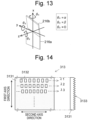
- the two-dimensional slits 113 and 213 in which the openings are disposed in a lattice pattern are used, but as shown in Fig. 14 , a two-dimensional slit 323 in which sets of openings 3232 having different lengths and periods in the second axis direction are disposed side by side in the first axis direction of a base member 3231 can also be used.
- the length and period in the second axis direction are determined for one wavelength ⁇ included in the object light.
- the rays of light of the wavelength ⁇ mainly intensify each other in all the linear interference images obtained from the plurality of measurement points disposed in the first axis direction.
- a slit in which openings are one-dimensionally disposed only in the second axis direction may be used.
- a line detector in which a plurality of pixels are disposed only in the second axis direction can be used.
- the amplitude-type diffraction grating may have any configuration as long as translucent portions and the light-shielding portions are alternately arrayed one-dimensionally or two-dimensionally, and need not be provided with physically opened portions.
- a multi-slit or a two-dimensional slit can be formed by applying, to a surface of a base member made of a material that transmits light in the wavelength band of the object light emitted from a measurement point on the surface of the sample, a mask made of a material that does not transmit light in the wavelength band of the object light and having openings arrayed one-dimensionally or two-dimensionally.
- a material including a single crystal of silicon having a surface on which gold is deposited is used, but a material on which metal other than gold (for example, aluminum) is deposited can also be used. Alternatively, a material made only of metal such as gold may be used.
- the material is not limited to pure metal, and it is also possible to use any kind of metal having free electrons such as stainless steel (SUS) is deposited or a material made of stainless steel or the like.
- SUS stainless steel
- a surface of the slit 13 or the two-dimensional slit 113 or 213 facing the two-dimensional detector 18, 118, or 218 may be sandblasted to form a rough surface, or the surface may be given an inclination to reflect light in a direction different from the direction to the two-dimensional detector 18, 118, or 218.
- an appropriate antireflection film may be formed on the surface instead of the subwavelength structure. In the case of forming the antireflection film, it is preferable to use a material having an emissivity smaller than that of silicon or to adopt a configuration of cooling the amplitude-type diffraction grating on which the antireflection film is formed.
- a thermal-type detector is used as the two-dimensional detector 18, 118, or 218, but a quantum-type two-dimensional detector may be used.
- the quantum-type two-dimensional detector for example, an MCT detector, an InSb-type detector, a CCD detector, or a CMOS detector can be used. Since these quantum-type detectors photoelectrically convert incident infrared rays to generate electric signals and detect the electric signals, it is unlikely that radiation light is generated from the detector.
- the quantum type detector it is necessary to use a cooling mechanism for suppressing generation of thermal noise, so that the device becomes expensive. Therefore, in order to suppress the cost of the device, it is preferable to use the two-dimensional detector 18, 118, or 218 that is a thermal-type detector, as in the above example.
- Amplitude-type diffraction gratings 41 to 47 of seven embodiments that can be adopted in the spectrometry device according to the present invention will be described with reference to Figs. 15A to 15H .
- the amplitude-type diffraction gratings described below may be a multi-slit (in which openings are disposed one-dimensionally) as used in the first example, or may be a two-dimensional slit (in which openings are disposed two-dimensionally) as used in the second example and the third example.
- a light-shielding member is constituted only by a member (absorbing member) 411 made of a material having an absorptivity larger than that of silicon in the wavelength band of the object light, and a plurality of openings are provided in the light-shielding member.
- a member for example, quartz glass or various organic compounds can be used.
- the amplitude-type diffraction grating 41 since an absorbing member 411 made of a material having an absorptivity higher than that of silicon is used, it is possible to absorb (block) more object light emitted from the sample and entering the light-shielding portion of the amplitude-type diffraction grating 41 than in the conventional case of using a light-shielding member made of a single crystal of silicon, so that the definition of the interference image can be increased as compared with the conventional case. Even when radiation light is emitted from the photodetector, the radiation light is absorbed by the absorbing member 411. Therefore, the radiation light from the photodetector does not re-enter the photodetector, so that the definition of the interference light does not deteriorate.
- the object light incident on the light-shielding portion can be absorbed sufficiently by using an absorbing member made from a quartz glass having a thickness of about 0.1 mm in general.
- an absorbing member made from a quartz glass having a thickness of about 0.1 mm in general.
- Many of the above-described materials having high light absorptivity have high emissivity.
- the intensity of the object light is high, it is necessary to increase the thickness of the absorbing member 411 in order to absorb the object light incident on the light-shielding portion of the amplitude-type diffraction grating 41.
- the amount of radiation light emitted from the absorbing member 411 increases, and there is a possibility that the definition of the interference image is reduced.
- a photodetector configured to selectively cool only a pixel on which light passing through the light-shielding portion is incident among a plurality of pixels included in the photodetector may be used.
- the configuration for cooling the photodetector has been described, but it is not realistic to cool the photodetector to absolute zero. That is, even if the photodetector is cooled, some radiation light is emitted.
- the intensity of the object light is weak, it is also conceivable to reverse this relationship.
- a member (reflection member) 422 made of a material (for example, metal such as gold; the same applies to the following embodiments) having a reflectance higher than that of silicon in the wavelength band of the object light is disposed on a side of a light incident face on which the object light is incident, and an absorbing member 421 is disposed on a side of a light emission face from which the object light is emitted.
- the amplitude-type diffraction grating 42 since most of the object light incident on the light-shielding portion of the amplitude-type diffraction grating 41 is reflected by the reflection member 422, it is not necessary to increase the thickness of the absorbing member 421 even when the intensity of the object light is large.
- the thin absorbing member 421 of about 0.1 mm can be used, the amount of radiation light emitted from the absorbing member 421 is sufficiently small, but the definition of interference light may be increased by further providing a diffraction grating cooling unit.
- the amplitude-type diffraction grating 43 of the third embodiment is obtained by combining an absorbing member 431 with a plate-like member (silicon member) 433 made of a single crystal of silicon.
- the absorbing member 431 having a thickness of about 0.1 mm can absorb the object light incident on the light-shielding portion, but is easily damaged because of the low strength, and is difficult to handle.
- the absorbing member 431 can be reinforced to have sufficient strength in combination with the silicon member 433.
- a silicon member used as a light-shielding member in a conventional amplitude-type diffraction grating is used as it is as a reinforcement member is illustrated, but a material and a shape of the reinforcement member can be appropriately changed.
- a frame-shaped member or the like that reinforces the peripheral portion of the absorbing member 431 can also be used.
- the amplitude-type diffraction grating 44 of the fourth embodiment is a combination of the second embodiment and the third embodiment, in which a silicon member 443, a reflection member 442, and an absorbing member 441 are disposed in order from a side on which the object light is incident.
- a silicon member 443, a reflection member 442, and an absorbing member 441 are disposed in order from a side on which the object light is incident.
- the amplitude-type diffraction grating 45 of the fifth embodiment is also a combination of the second embodiment and the third embodiment, in which a reflection member 452, a silicon member 453, and an absorbing member 451 are disposed in order from a side on which the object light is incident. Also in the amplitude-type diffraction grating 45, both of the effects obtained in the second embodiment and the third embodiment can be obtained.
- a reflection member 462 is disposed on a side on which the object light is incident, and a silicon member 463 is disposed on a side from which the object light is emitted.
- the object light is reflected at light-shielding portions of the reflection member 462 with a high reflectance, and the object light hardly reaches light-shielding portions of the silicon member 463. Therefore, the amplitude-type diffraction grating 46 can obtain an interference image having high definition as compared with the conventional amplitude-type diffraction grating formed only of the silicon member.
- the single crystal of silicon is exposed on the side of the face from which the object light is emitted. Since silicon is a material having high thermal radiation (high emissivity), more radiation light is emitted from the silicon member 463 as the temperature becomes higher. When this radiation light is incident on a photodetector, the definition of the interference image decreases. In addition, since silicon is a material having a high reflectance, when radiation light is emitted from the photodetector, there is a possibility that the radiation light is reflected by the amplitude-type diffraction grating 46 and enters the photodetector again. When this reflected light is incident on the photodetector, the definition of the interference image decreases.
- the amplitude-type diffraction grating 46 of this embodiment it is preferable to adopt a configuration including a cooling unit configured to cool the amplitude-type diffraction grating 46 and/or the photodetector.
- a silicon member 473 is disposed on a side on which the object light is incident, and a reflection member 472 is disposed on a side from which the object light is emitted.
- the amplitude-type diffraction grating 47 even if the object light passes through light-shielding portions (portions other than openings) of the silicon member 473, the object light is reflected by light-shielding portions of the reflection member 472. Therefore, the amplitude-type diffraction grating 47 can obtain an interference image having high definition as compared with the conventional amplitude-type diffraction grating formed only of the silicon member.
- the amplitude-type diffraction grating 47 when light in the same wavelength band (infrared region) as the object light is radiated (thermally radiated) from the photodetector as in a thermal-type photodetector, there is a possibility that the light is directly reflected by the reflection member and is incident on the photodetector again. Therefore, when the amplitude-type diffraction grating 47 is used in combination with the thermal-type photodetector or the like, it is preferable to adopt a configuration in which the photodetector is cooled to suppress thermal radiation.
- a silicon member 483 is disposed on a side on which the object light is incident, and a reflection member 482 is disposed on a side from which the object light is emitted, and an antireflection portion 484 is provided to a surface (light emission face) of the reflection member 482.
- the antireflection portion 484 only needs to suppress direct reflection of incident light, and various antireflection portions can be used.
- the light emission face side of the antireflection portion 484 is provided with the sub-wavelength structure (SWC) described in the above examples, the light emission face is sandblasted, or the light emission face is inclined, and thereby the antireflection portion 484 can be provided.
- SWC sub-wavelength structure
- the antireflection portion 484 can prevent the radiation light from entering the photodetector again.
- a metal such as gold that is, a material having a small emissivity is located on the light emission face side, the thermal radiation from the amplitude-type diffraction grating 48 is also small. Therefore, it is possible to obtain an interference image with sufficiently high definition without cooling the amplitude-type diffraction grating 48 and the photodetector.
Landscapes
- Physics & Mathematics (AREA)
- Spectroscopy & Molecular Physics (AREA)
- General Physics & Mathematics (AREA)
- Health & Medical Sciences (AREA)
- Life Sciences & Earth Sciences (AREA)
- Chemical & Material Sciences (AREA)
- Analytical Chemistry (AREA)
- Biochemistry (AREA)
- General Health & Medical Sciences (AREA)
- Immunology (AREA)
- Pathology (AREA)
- Investigating Or Analysing Materials By Optical Means (AREA)
Applications Claiming Priority (2)
| Application Number | Priority Date | Filing Date | Title |
|---|---|---|---|
| JP2021149236 | 2021-09-14 | ||
| PCT/JP2022/032916 WO2023042668A1 (ja) | 2021-09-14 | 2022-09-01 | 分光測定装置 |
Publications (2)
| Publication Number | Publication Date |
|---|---|
| EP4403891A1 true EP4403891A1 (de) | 2024-07-24 |
| EP4403891A4 EP4403891A4 (de) | 2025-03-26 |
Family
ID=85602800
Family Applications (1)
| Application Number | Title | Priority Date | Filing Date |
|---|---|---|---|
| EP22869815.5A Pending EP4403891A4 (de) | 2021-09-14 | 2022-09-01 | Spektrometrievorrichtung |
Country Status (5)
| Country | Link |
|---|---|
| US (1) | US12158417B1 (de) |
| EP (1) | EP4403891A4 (de) |
| JP (1) | JPWO2023042668A1 (de) |
| CN (1) | CN117957427B (de) |
| WO (1) | WO2023042668A1 (de) |
Family Cites Families (19)
| Publication number | Priority date | Publication date | Assignee | Title |
|---|---|---|---|---|
| US6687010B1 (en) * | 1999-09-09 | 2004-02-03 | Olympus Corporation | Rapid depth scanning optical imaging device |
| US6559952B1 (en) * | 2000-05-11 | 2003-05-06 | The Regents Of The University Of California | System for interferometric distortion measurements that define an optical path |
| JP4608679B2 (ja) | 2005-03-17 | 2011-01-12 | 財団法人新産業創造研究機構 | X線タルボ干渉計に用いられる位相型回折格子と振幅型回折格子の製造方法 |
| JP2007067123A (ja) * | 2005-08-31 | 2007-03-15 | National Institute Of Advanced Industrial & Technology | レーザーパルス圧縮装置 |
| CA2600900A1 (en) | 2006-09-21 | 2008-03-21 | Nippon Sheet Glass Company, Limited | Transmissive diffraction grating, and spectral separation element and spectroscope using the same |
| JP5280654B2 (ja) * | 2006-09-21 | 2013-09-04 | 日本板硝子株式会社 | 透過型回折格子、並びに、それを用いた分光素子及び分光器 |
| US8154732B2 (en) * | 2007-04-27 | 2012-04-10 | Bodkin Design And Engineering, Llc | Multiband spatial heterodyne spectrometer and associated methods |
| JP2008282322A (ja) | 2007-05-14 | 2008-11-20 | Sony Ericsson Mobilecommunications Japan Inc | 情報処理装置及び情報処理方法 |
| JP5120873B2 (ja) | 2007-06-15 | 2013-01-16 | 国立大学法人 香川大学 | 分光計測装置及び分光計測方法 |
| JP2009282322A (ja) * | 2008-05-22 | 2009-12-03 | Konica Minolta Medical & Graphic Inc | 振幅型回折格子の製造方法 |
| JP5317298B2 (ja) | 2010-09-08 | 2013-10-16 | 国立大学法人 香川大学 | 分光計測装置及び分光計測方法 |
| US20130188181A1 (en) * | 2011-10-18 | 2013-07-25 | Stanley Michael Angel | Systems and Methods for Spatial Heterodyne Raman Spectroscopy |
| EP2982949B1 (de) * | 2012-10-05 | 2020-04-15 | National University Corporation Kagawa University | Spektroskopische messvorrichtung |
| US9482576B2 (en) * | 2012-10-05 | 2016-11-01 | National University Corporation Kagawa University | Spectroscopic measurement device having transmissive optical member with a sloped face |
| JP2014142338A (ja) * | 2012-12-27 | 2014-08-07 | Canon Inc | 干渉計及び被検体情報取得システム |
| JP6385288B2 (ja) | 2015-01-29 | 2018-09-05 | 国立大学法人 香川大学 | 分光特性測定装置 |
| WO2017007024A1 (ja) | 2015-07-08 | 2017-01-12 | 国立大学法人香川大学 | 分光測定装置 |
| CN114341602B (zh) * | 2019-09-03 | 2024-04-02 | 国立大学法人香川大学 | 分光测定装置 |
| JP7453659B2 (ja) * | 2019-11-21 | 2024-03-21 | 国立大学法人 香川大学 | 輻射光検出装置 |
-
2022
- 2022-09-01 JP JP2023548400A patent/JPWO2023042668A1/ja active Pending
- 2022-09-01 WO PCT/JP2022/032916 patent/WO2023042668A1/ja not_active Ceased
- 2022-09-01 EP EP22869815.5A patent/EP4403891A4/de active Pending
- 2022-09-01 CN CN202280062448.9A patent/CN117957427B/zh active Active
- 2022-09-01 US US18/691,179 patent/US12158417B1/en active Active
Also Published As
| Publication number | Publication date |
|---|---|
| US20240385107A1 (en) | 2024-11-21 |
| EP4403891A4 (de) | 2025-03-26 |
| US12158417B1 (en) | 2024-12-03 |
| JPWO2023042668A1 (de) | 2023-03-23 |
| WO2023042668A1 (ja) | 2023-03-23 |
| CN117957427B (zh) | 2025-04-29 |
| CN117957427A (zh) | 2024-04-30 |
Similar Documents
| Publication | Publication Date | Title |
|---|---|---|
| US7420677B2 (en) | Sensing photon energies of optical signals | |
| JP5635624B2 (ja) | 小型干渉分光計 | |
| EP2908107B1 (de) | Vorrichtung zur messung spektraler eigenschaften | |
| US10908019B2 (en) | Spectrometer and spectrum measurement method utilizing same | |
| US11629996B2 (en) | Compact hyperspectral mid-infrared spectrometer | |
| JP2013513112A (ja) | ファブリーペローフーリエ変換分光計 | |
| US12055437B2 (en) | Spectrometer and imaging device | |
| TWI670483B (zh) | 光學干涉裝置、相移陣列及用以產生空間分佈干涉光圖樣之方法 | |
| US20210270736A1 (en) | Diffractive biosensor | |
| JP6732339B2 (ja) | 分光測定装置 | |
| JP2017156245A (ja) | 分光測定装置 | |
| EP4403891A1 (de) | Spektrometrievorrichtung | |
| JP7669039B2 (ja) | 分光測定装置 | |
| EP3809103B1 (de) | Spektrometer und spektroskopisches verfahren | |
| JP6036308B2 (ja) | 赤外線センサ及び温度補償方法 | |
| JPH07103824A (ja) | 分光器 | |
| JPWO2021044979A5 (de) | ||
| Workman | Optical spectrometers | |
| JPWO2023042668A5 (de) | ||
| US12044580B2 (en) | Method and system for measuring the temperature of a thermochromic liquid crystal | |
| JP2009128193A (ja) | 波長センサ |
Legal Events
| Date | Code | Title | Description |
|---|---|---|---|
| STAA | Information on the status of an ep patent application or granted ep patent |
Free format text: STATUS: THE INTERNATIONAL PUBLICATION HAS BEEN MADE |
|
| PUAI | Public reference made under article 153(3) epc to a published international application that has entered the european phase |
Free format text: ORIGINAL CODE: 0009012 |
|
| STAA | Information on the status of an ep patent application or granted ep patent |
Free format text: STATUS: REQUEST FOR EXAMINATION WAS MADE |
|
| 17P | Request for examination filed |
Effective date: 20240412 |
|
| AK | Designated contracting states |
Kind code of ref document: A1 Designated state(s): AL AT BE BG CH CY CZ DE DK EE ES FI FR GB GR HR HU IE IS IT LI LT LU LV MC MK MT NL NO PL PT RO RS SE SI SK SM TR |
|
| DAV | Request for validation of the european patent (deleted) | ||
| DAX | Request for extension of the european patent (deleted) | ||
| A4 | Supplementary search report drawn up and despatched |
Effective date: 20250226 |
|
| RIC1 | Information provided on ipc code assigned before grant |
Ipc: G01J 3/02 20060101ALI20250220BHEP Ipc: G01J 3/453 20060101AFI20250220BHEP |