EP4401078A1 - Chip packaging structure and manufacturing method therefor, and electronic device - Google Patents
Chip packaging structure and manufacturing method therefor, and electronic device Download PDFInfo
- Publication number
- EP4401078A1 EP4401078A1 EP22871070.3A EP22871070A EP4401078A1 EP 4401078 A1 EP4401078 A1 EP 4401078A1 EP 22871070 A EP22871070 A EP 22871070A EP 4401078 A1 EP4401078 A1 EP 4401078A1
- Authority
- EP
- European Patent Office
- Prior art keywords
- chip
- package
- package substrate
- layer
- electrically connected
- Prior art date
- Legal status (The legal status is an assumption and is not a legal conclusion. Google has not performed a legal analysis and makes no representation as to the accuracy of the status listed.)
- Granted
Links
Images





Classifications
-
- H—ELECTRICITY
- H10—SEMICONDUCTOR DEVICES; ELECTRIC SOLID-STATE DEVICES NOT OTHERWISE PROVIDED FOR
- H10W—GENERIC PACKAGES, INTERCONNECTIONS, CONNECTORS OR OTHER CONSTRUCTIONAL DETAILS OF DEVICES COVERED BY CLASS H10
- H10W20/00—Interconnections in chips, wafers or substrates
- H10W20/40—Interconnections external to wafers or substrates, e.g. back-end-of-line [BEOL] metallisations or vias connecting to gate electrodes
- H10W20/41—Interconnections external to wafers or substrates, e.g. back-end-of-line [BEOL] metallisations or vias connecting to gate electrodes characterised by their conductive parts
- H10W20/427—Power or ground buses
-
- H—ELECTRICITY
- H10—SEMICONDUCTOR DEVICES; ELECTRIC SOLID-STATE DEVICES NOT OTHERWISE PROVIDED FOR
- H10W—GENERIC PACKAGES, INTERCONNECTIONS, CONNECTORS OR OTHER CONSTRUCTIONAL DETAILS OF DEVICES COVERED BY CLASS H10
- H10W20/00—Interconnections in chips, wafers or substrates
- H10W20/01—Manufacture or treatment
- H10W20/021—Manufacture or treatment of interconnections within wafers or substrates
- H10W20/023—Manufacture or treatment of interconnections within wafers or substrates the interconnections being through-semiconductor vias
-
- H—ELECTRICITY
- H10—SEMICONDUCTOR DEVICES; ELECTRIC SOLID-STATE DEVICES NOT OTHERWISE PROVIDED FOR
- H10W—GENERIC PACKAGES, INTERCONNECTIONS, CONNECTORS OR OTHER CONSTRUCTIONAL DETAILS OF DEVICES COVERED BY CLASS H10
- H10W42/00—Arrangements for protection of devices
- H10W42/20—Arrangements for protection of devices protecting against electromagnetic or particle radiation, e.g. light, X-rays, gamma-rays or electrons
-
- H—ELECTRICITY
- H10—SEMICONDUCTOR DEVICES; ELECTRIC SOLID-STATE DEVICES NOT OTHERWISE PROVIDED FOR
- H10W—GENERIC PACKAGES, INTERCONNECTIONS, CONNECTORS OR OTHER CONSTRUCTIONAL DETAILS OF DEVICES COVERED BY CLASS H10
- H10W42/00—Arrangements for protection of devices
- H10W42/20—Arrangements for protection of devices protecting against electromagnetic or particle radiation, e.g. light, X-rays, gamma-rays or electrons
- H10W42/261—Arrangements for protection of devices protecting against electromagnetic or particle radiation, e.g. light, X-rays, gamma-rays or electrons characterised by their shapes or dispositions
- H10W42/276—Arrangements for protection of devices protecting against electromagnetic or particle radiation, e.g. light, X-rays, gamma-rays or electrons characterised by their shapes or dispositions the arrangements being on an external surface of the package, e.g. on the outer surface of an encapsulation
-
- H—ELECTRICITY
- H10—SEMICONDUCTOR DEVICES; ELECTRIC SOLID-STATE DEVICES NOT OTHERWISE PROVIDED FOR
- H10W—GENERIC PACKAGES, INTERCONNECTIONS, CONNECTORS OR OTHER CONSTRUCTIONAL DETAILS OF DEVICES COVERED BY CLASS H10
- H10W70/00—Package substrates; Interposers; Redistribution layers [RDL]
- H10W70/01—Manufacture or treatment
- H10W70/05—Manufacture or treatment of insulating or insulated package substrates, or of interposers, or of redistribution layers
-
- H—ELECTRICITY
- H10—SEMICONDUCTOR DEVICES; ELECTRIC SOLID-STATE DEVICES NOT OTHERWISE PROVIDED FOR
- H10W—GENERIC PACKAGES, INTERCONNECTIONS, CONNECTORS OR OTHER CONSTRUCTIONAL DETAILS OF DEVICES COVERED BY CLASS H10
- H10W70/00—Package substrates; Interposers; Redistribution layers [RDL]
- H10W70/60—Insulating or insulated package substrates; Interposers; Redistribution layers
- H10W70/611—Insulating or insulated package substrates; Interposers; Redistribution layers for connecting multiple chips together
-
- H—ELECTRICITY
- H10—SEMICONDUCTOR DEVICES; ELECTRIC SOLID-STATE DEVICES NOT OTHERWISE PROVIDED FOR
- H10W—GENERIC PACKAGES, INTERCONNECTIONS, CONNECTORS OR OTHER CONSTRUCTIONAL DETAILS OF DEVICES COVERED BY CLASS H10
- H10W70/00—Package substrates; Interposers; Redistribution layers [RDL]
- H10W70/60—Insulating or insulated package substrates; Interposers; Redistribution layers
- H10W70/67—Insulating or insulated package substrates; Interposers; Redistribution layers characterised by their insulating layers or insulating parts
- H10W70/68—Shapes or dispositions thereof
- H10W70/685—Shapes or dispositions thereof comprising multiple insulating layers
-
- H—ELECTRICITY
- H10—SEMICONDUCTOR DEVICES; ELECTRIC SOLID-STATE DEVICES NOT OTHERWISE PROVIDED FOR
- H10W—GENERIC PACKAGES, INTERCONNECTIONS, CONNECTORS OR OTHER CONSTRUCTIONAL DETAILS OF DEVICES COVERED BY CLASS H10
- H10W72/00—Interconnections or connectors in packages
- H10W72/20—Bump connectors, e.g. solder bumps or copper pillars; Dummy bumps; Thermal bumps
-
- H—ELECTRICITY
- H10—SEMICONDUCTOR DEVICES; ELECTRIC SOLID-STATE DEVICES NOT OTHERWISE PROVIDED FOR
- H10W—GENERIC PACKAGES, INTERCONNECTIONS, CONNECTORS OR OTHER CONSTRUCTIONAL DETAILS OF DEVICES COVERED BY CLASS H10
- H10W72/00—Interconnections or connectors in packages
- H10W72/851—Dispositions of multiple connectors or interconnections
-
- H—ELECTRICITY
- H10—SEMICONDUCTOR DEVICES; ELECTRIC SOLID-STATE DEVICES NOT OTHERWISE PROVIDED FOR
- H10W—GENERIC PACKAGES, INTERCONNECTIONS, CONNECTORS OR OTHER CONSTRUCTIONAL DETAILS OF DEVICES COVERED BY CLASS H10
- H10W74/00—Encapsulations, e.g. protective coatings
- H10W74/01—Manufacture or treatment
- H10W74/012—Manufacture or treatment of encapsulations on active surfaces of flip-chip devices, e.g. forming underfills
-
- H—ELECTRICITY
- H10—SEMICONDUCTOR DEVICES; ELECTRIC SOLID-STATE DEVICES NOT OTHERWISE PROVIDED FOR
- H10W—GENERIC PACKAGES, INTERCONNECTIONS, CONNECTORS OR OTHER CONSTRUCTIONAL DETAILS OF DEVICES COVERED BY CLASS H10
- H10W74/00—Encapsulations, e.g. protective coatings
- H10W74/01—Manufacture or treatment
- H10W74/016—Manufacture or treatment using moulds
-
- H—ELECTRICITY
- H10—SEMICONDUCTOR DEVICES; ELECTRIC SOLID-STATE DEVICES NOT OTHERWISE PROVIDED FOR
- H10W—GENERIC PACKAGES, INTERCONNECTIONS, CONNECTORS OR OTHER CONSTRUCTIONAL DETAILS OF DEVICES COVERED BY CLASS H10
- H10W74/00—Encapsulations, e.g. protective coatings
- H10W74/10—Encapsulations, e.g. protective coatings characterised by their shape or disposition
- H10W74/111—Encapsulations, e.g. protective coatings characterised by their shape or disposition the semiconductor body being completely enclosed
- H10W74/114—Encapsulations, e.g. protective coatings characterised by their shape or disposition the semiconductor body being completely enclosed by a substrate and the encapsulations
- H10W74/117—Encapsulations, e.g. protective coatings characterised by their shape or disposition the semiconductor body being completely enclosed by a substrate and the encapsulations the substrate having spherical bumps for external connection
-
- H—ELECTRICITY
- H10—SEMICONDUCTOR DEVICES; ELECTRIC SOLID-STATE DEVICES NOT OTHERWISE PROVIDED FOR
- H10W—GENERIC PACKAGES, INTERCONNECTIONS, CONNECTORS OR OTHER CONSTRUCTIONAL DETAILS OF DEVICES COVERED BY CLASS H10
- H10W74/00—Encapsulations, e.g. protective coatings
- H10W74/10—Encapsulations, e.g. protective coatings characterised by their shape or disposition
- H10W74/15—Encapsulations, e.g. protective coatings characterised by their shape or disposition on active surfaces of flip-chip devices, e.g. underfills
-
- H—ELECTRICITY
- H10—SEMICONDUCTOR DEVICES; ELECTRIC SOLID-STATE DEVICES NOT OTHERWISE PROVIDED FOR
- H10W—GENERIC PACKAGES, INTERCONNECTIONS, CONNECTORS OR OTHER CONSTRUCTIONAL DETAILS OF DEVICES COVERED BY CLASS H10
- H10W90/00—Package configurations
-
- H—ELECTRICITY
- H10—SEMICONDUCTOR DEVICES; ELECTRIC SOLID-STATE DEVICES NOT OTHERWISE PROVIDED FOR
- H10W—GENERIC PACKAGES, INTERCONNECTIONS, CONNECTORS OR OTHER CONSTRUCTIONAL DETAILS OF DEVICES COVERED BY CLASS H10
- H10W90/00—Package configurations
- H10W90/701—Package configurations characterised by the relative positions of pads or connectors relative to package parts
-
- G—PHYSICS
- G11—INFORMATION STORAGE
- G11C—STATIC STORES
- G11C5/00—Details of stores covered by group G11C11/00
- G11C5/02—Disposition of storage elements, e.g. in the form of a matrix array
- G11C5/04—Supports for storage elements, e.g. memory modules; Mounting or fixing of storage elements on such supports
-
- H—ELECTRICITY
- H10—SEMICONDUCTOR DEVICES; ELECTRIC SOLID-STATE DEVICES NOT OTHERWISE PROVIDED FOR
- H10W—GENERIC PACKAGES, INTERCONNECTIONS, CONNECTORS OR OTHER CONSTRUCTIONAL DETAILS OF DEVICES COVERED BY CLASS H10
- H10W70/00—Package substrates; Interposers; Redistribution layers [RDL]
- H10W70/60—Insulating or insulated package substrates; Interposers; Redistribution layers
-
- H—ELECTRICITY
- H10—SEMICONDUCTOR DEVICES; ELECTRIC SOLID-STATE DEVICES NOT OTHERWISE PROVIDED FOR
- H10W—GENERIC PACKAGES, INTERCONNECTIONS, CONNECTORS OR OTHER CONSTRUCTIONAL DETAILS OF DEVICES COVERED BY CLASS H10
- H10W72/00—Interconnections or connectors in packages
- H10W72/823—Interconnections through encapsulations, e.g. pillars through molded resin on a lateral side a chip
-
- H—ELECTRICITY
- H10—SEMICONDUCTOR DEVICES; ELECTRIC SOLID-STATE DEVICES NOT OTHERWISE PROVIDED FOR
- H10W—GENERIC PACKAGES, INTERCONNECTIONS, CONNECTORS OR OTHER CONSTRUCTIONAL DETAILS OF DEVICES COVERED BY CLASS H10
- H10W72/00—Interconnections or connectors in packages
- H10W72/851—Dispositions of multiple connectors or interconnections
- H10W72/853—On the same surface
- H10W72/856—Bump connectors and die-attach connectors
-
- H—ELECTRICITY
- H10—SEMICONDUCTOR DEVICES; ELECTRIC SOLID-STATE DEVICES NOT OTHERWISE PROVIDED FOR
- H10W—GENERIC PACKAGES, INTERCONNECTIONS, CONNECTORS OR OTHER CONSTRUCTIONAL DETAILS OF DEVICES COVERED BY CLASS H10
- H10W90/00—Package configurations
- H10W90/20—Configurations of stacked chips
- H10W90/24—Configurations of stacked chips at least one of the stacked chips being laterally offset from a neighbouring stacked chip, e.g. chip stacks having a staircase shape
-
- H—ELECTRICITY
- H10—SEMICONDUCTOR DEVICES; ELECTRIC SOLID-STATE DEVICES NOT OTHERWISE PROVIDED FOR
- H10W—GENERIC PACKAGES, INTERCONNECTIONS, CONNECTORS OR OTHER CONSTRUCTIONAL DETAILS OF DEVICES COVERED BY CLASS H10
- H10W90/00—Package configurations
- H10W90/20—Configurations of stacked chips
- H10W90/297—Configurations of stacked chips characterised by the through-semiconductor vias [TSVs] in the stacked chips
-
- H—ELECTRICITY
- H10—SEMICONDUCTOR DEVICES; ELECTRIC SOLID-STATE DEVICES NOT OTHERWISE PROVIDED FOR
- H10W—GENERIC PACKAGES, INTERCONNECTIONS, CONNECTORS OR OTHER CONSTRUCTIONAL DETAILS OF DEVICES COVERED BY CLASS H10
- H10W90/00—Package configurations
- H10W90/701—Package configurations characterised by the relative positions of pads or connectors relative to package parts
- H10W90/721—Package configurations characterised by the relative positions of pads or connectors relative to package parts of bump connectors
- H10W90/722—Package configurations characterised by the relative positions of pads or connectors relative to package parts of bump connectors between stacked chips
-
- H—ELECTRICITY
- H10—SEMICONDUCTOR DEVICES; ELECTRIC SOLID-STATE DEVICES NOT OTHERWISE PROVIDED FOR
- H10W—GENERIC PACKAGES, INTERCONNECTIONS, CONNECTORS OR OTHER CONSTRUCTIONAL DETAILS OF DEVICES COVERED BY CLASS H10
- H10W90/00—Package configurations
- H10W90/701—Package configurations characterised by the relative positions of pads or connectors relative to package parts
- H10W90/721—Package configurations characterised by the relative positions of pads or connectors relative to package parts of bump connectors
- H10W90/724—Package configurations characterised by the relative positions of pads or connectors relative to package parts of bump connectors between a chip and a stacked insulating package substrate, interposer or RDL
-
- H—ELECTRICITY
- H10—SEMICONDUCTOR DEVICES; ELECTRIC SOLID-STATE DEVICES NOT OTHERWISE PROVIDED FOR
- H10W—GENERIC PACKAGES, INTERCONNECTIONS, CONNECTORS OR OTHER CONSTRUCTIONAL DETAILS OF DEVICES COVERED BY CLASS H10
- H10W90/00—Package configurations
- H10W90/701—Package configurations characterised by the relative positions of pads or connectors relative to package parts
- H10W90/731—Package configurations characterised by the relative positions of pads or connectors relative to package parts of die-attach connectors
- H10W90/734—Package configurations characterised by the relative positions of pads or connectors relative to package parts of die-attach connectors between a chip and a stacked insulating package substrate, interposer or RDL
-
- H—ELECTRICITY
- H10—SEMICONDUCTOR DEVICES; ELECTRIC SOLID-STATE DEVICES NOT OTHERWISE PROVIDED FOR
- H10W—GENERIC PACKAGES, INTERCONNECTIONS, CONNECTORS OR OTHER CONSTRUCTIONAL DETAILS OF DEVICES COVERED BY CLASS H10
- H10W90/00—Package configurations
- H10W90/701—Package configurations characterised by the relative positions of pads or connectors relative to package parts
- H10W90/751—Package configurations characterised by the relative positions of pads or connectors relative to package parts of bond wires
- H10W90/754—Package configurations characterised by the relative positions of pads or connectors relative to package parts of bond wires between a chip and a stacked insulating package substrate, interposer or RDL
Definitions
- the present disclosure relates to the field of semiconductor technologies, and particularly relates to a chip package structure, a manufacturing method thereof, and an electronic device.
- Embodiments of the present disclosure provide a chip package structure, a manufacturing method thereof, and an electronic device, for the purposes of reducing the area of the chip package structure and improving the rate of signal transmission.
- a chip package structure in an aspect, includes a package substrate, a first chip, a conductive pillar and a second chip, wherein the package substrate has a first surface; the first chip is located on the first surface of the package substrate and electrically connected to the package substrate; the conductive pillar is located on the first surface of the package substrate and electrically connected to the package substrate; the second chip is located on a side of the first chip and the conductive pillar away from the package substrate and electrically connected to the conductive pillar; and an orthographic projection of the conductive pillar on the package substrate is located within a range of an orthographic projection of the first chip or the second chip on the package substrate.
- the second chip is placed above the first chip, such that the package substrate, the first chip, the conductive pillar and the second chip form a stacked structure, which improves the compactness of the chip package structure and helps to reduce the area of the chip package structure.
- the conductive pillar is provided to realize the electrical connection between the second chip and the package substrate, and the conductive pillar is disposed under the first chip 2 or the second chip such that the orthographic projection of the conductive pillar on the package substrate is located within the range of the orthographic projection of the first chip 2 or the second chip on the package substrate. In this way, the space around the first chip 2 or the second chip may not be occupied, which helps to further miniaturize the chip package structure and to further reduce the area of the chip package structure.
- an orthographic projection of the conductive pillar on the package substrate is also located within a range of an orthographic projection of the first chip on the package substrate.
- the chip package structure further includes a package layer, and the package layer is located between the package substrate and the second chip, covers the first chip and surrounds sides of the conductive pillar.
- an orthographic projection of the second chip on the package substrate is located within a range of an orthographic projection of the package layer on the package substrate.
- the chip package structure further includes a first filling portion, and at least part of the first filling portion is located between the package layer and the second chip and the first filling portion surrounds each pin of the second chip.
- the chip package structure further includes an electromagnetic shielding layer, and the electromagnetic shielding layer at least covers the second chip as well as sides of the package layer.
- the package substrate further includes at least one ground wire, and the electromagnetic shielding layer also covers sides of the package substrate and is electrically connected to the ground wire.
- the second chip comprises a plurality of sub-chips sequentially stacked in a direction perpendicular to and away from the package substrate.
- two adjacent sub-chips are electrically connected to each other.
- one of the plurality of sub-chips close to the package substrate is electrically connected to the conductive pillar, and others of the plurality of sub-chips are electrically connected to the package substrate by a wire.
- a surface on a side of the second chip close to the package substrate is higher than a surface on a side of the first chip away from the package substrate, with respect to the first surface of the package substrate.
- a distance between the surface on the side of the second chip close to the package substrate and the first surface of the package substrate is h1
- a distance between the surface on the side of the first chip away from the package substrate and the first surface of the package substrate is h2
- h1 and h2 meet the following condition: 5 8 ⁇ h 2 h 1 ⁇ 4 5 .
- a number of the conductive pillars is greater than one, and the plurality of conductive pillars are at least located on two opposite sides of the first chip.
- the chip package structure further includes a second filling portion, and at least part of the second filling portion is located between the package substrate and the first chip and the second filling portion surrounds each pin of the first chip.
- the package substrate has a second surface opposite to the first surface
- the chip package structure further comprises a solder ball located on the second surface of the package surface and electrically connected to the package substrate.
- the chip package structure includes: a package substrate having a first surface; a first chip disposed on the first surface of the package substrate and electrically connected to the package substrate; and a second chipset located on a side of the first chip away from the package substrate, electrically connected to the package substrate, and comprising a plurality of second chips sequentially stacked in a direction perpendicular to and away from the package substrate.
- two adjacent second chips are electrically connected to each other.
- each of the plurality of second chips is electrically connected to the package substrate by a wire.
- the chip package structure further includes a package layer, and the package layer is located between the package substrate and the second chipset and covers the first chip.
- an orthographic projection of the second chipset on the package substrate is located within a range of an orthographic projection of the package layer on the package substrate.
- the chip package structure further includes a first filling portion, and at least part of the first filling portion is located between the package layer and the second chipset and the first filling portion surrounds each pin of one second chip close to the package substrate.
- the chip package structure further includes an electromagnetic shielding layer, the electromagnetic shielding layer at least covers the second chipset as well as sides of the package layer.
- the package substrate includes at least one ground wire
- the electromagnetic shielding layer also covers sides of the package substrate and is electrically connected to the ground wire.
- a surface on a side of the second chipset close to the package substrate is higher than a surface on a side of the first chip away from the package substrate, with respect to the first surface of the package substrate.
- a distance between the surface on the side of the second chipset close to the package substrate and the first surface of the package substrate is h1
- a distance between the surface on the side of the first chip away from the package substrate and the first surface of the package substrate is h2
- h1 and h2 meet the following condition: 5 8 ⁇ h 2 h 1 ⁇ 4 5 .
- the chip package structure further includes a second filling portion, and at least part of the second filling portion is located between the package substrate and the first chip and the second filling portion surrounds each pin of the first chip.
- the package substrate has a second surface opposite to the first surface
- the chip package structure further comprises a solder ball located on the second surface of the package surface and electrically connected to the package substrate.
- an electronic device in yet another aspect, includes the chip package structure as described in some embodiments above.
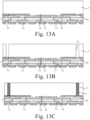
- a manufacturing method of a chip package structure includes: providing a package substrate having a first surface on which a first pad and a second pad are disposed at an interval; forming a conductive pillar on the first surface of the package structure, the conductive pillar being electrically connected to the second pad; disposing a first chip on the first surface of the package substrate, the first chip being electrically connected to the first pad; and disposing a second chip on a side of the conductive pillar and the first chip away from the package substrate, the second chip being electrically connected to the conductive pillar, an orthographic projection of the conductive pillar on the package substrate being located within a range of an orthographic projection of the second chip on the package substrate.
- the manufacturing method before the disposing the second chip on the side of the conductive pillar and the first chip away from the package substrate, the manufacturing method further comprises: forming a package film on the first chip and the conductive pillar, the package film covering the first chip and the conductive pillar; and thinning the package film to expose the conductive pillar and to obtain a package layer, the package layer covering the first chip.
- the forming the conductive pillar on the first surface of the package substrate comprises: forming a package layer on the first chip, the package layer covering the first chip; forming a via in the package layer, the via exposing a second pad; and filling the via with a conductive material to form the conductive pillar.
- the manufacturing method further includes: filling a first insulating material between the package layer and the second chip to form a first filling portion, the first filling portion surrounding each pin of the second chip.
- the manufacturing method further includes: forming an electromagnetic shielding layer, the electromagnetic shielding layer at least covering the second chip as well as sides of the package layer.
- the second chip comprises a plurality of sub-chips; and the disposing the second chip on the side of the conductive pillar and the first chip away from the package substrate comprises: sequentially stacking the plurality of sub-chips in a thickness direction of the sub-chips to form the second chip; and soldering the second chip with an end of the conductive pillar away from the package substrate, such that the second chip is electrically connected to the conductive pillar.
- the manufacturing method further includes: filling a second insulating material between the package substrate and the first chip to form a second filling portion, the second filling portion surrounding each pin of the first chip.
- a third pad is disposed on a second surface of the package substrate, and the first surface and the second surface are opposite to each other; and before or after forming the package layer, the manufacturing method further includes: forming a solder ball on the second surface of the package substrate, the solder ball being electrically connected to the third pad.
- the term “comprise” is interpreted as an open-ended inclusion, i.e., “comprising, but not limited to”.
- the terms “an embodiment”, “some embodiments”, “exemplary embodiments”, “exemplarily” or “some examples”, etc. are intended to indicate that a specific feature, structure, material or characteristic related to the embodiment or example is included in at least one embodiment or example of the present disclosure. Schematic representations of the above terms do not necessarily refer to the same embodiment or example.
- the specific feature, structure, material or characteristic described may be included in any one or more embodiments or examples in any appropriate manner.
- first and second are only intended for description and shall not be construed to indicate or imply relative importance, or imply the number of the indicated technical features. Therefore, the features defined by “first” and “second” can indicate or imply that one or more features are included. In the descriptions of the embodiments of the present disclosure, unless otherwise stated, "a plurality of" means two or more.
- connection In describing some embodiments, the expressions of "connect” and its extensions may be used. For example, some embodiments may be described by using the term “connect” to indicate that two or more components are in direct physical or electrical contact. For another example, some embodiments may be described by using the term “couple” to indicate that two or more components are in direct physical contact or electrical contact. However, the term “couple” may also mean that two or more components are not in direct contact but still cooperate or interact with each other. The embodiments disclosed herein are not necessarily limited to the content herein.
- At least one of A, B and C and “at least one of A, B or C” have the same meaning of including the following combinations of A, B and C: only A, only B, only C, a combination of A and B, a combination of A and C, a combination of B and C, and a combination of A, B and C.
- a and/or B includes the following three combinations: only A, only B, and a combination of A and B.
- a first chip 2' and a second chip 3' in a chip package structure 100' are typically disposed side by side on a package substrate 1' in a tiling manner.
- a plurality of gold fingers are disposed on a side of the package substrate 1' close to the first chip 2' and the second chip 3'.
- the first chip 2' and the second chip 3' are respectively connected to the gold fingers by gold wires 4' by using the WB (wire bonding) process, so that the first chip 2' and the second chip 3' may be electrically connected by the respectively connected gold wires 4' and the package substrate 1', thereby realizing communication between the first chip 2' and the second chip 3'.
- the first chip 2' and the second chip 3' are disposed side by side, which makes the area of the chip package structure 100' larger.
- the wire arcs of the gold wires 4' and the existence of the gold fingers it is necessary to reserve certain areas around the first chip 2' and the second chip 3', which further increases the area of the chip package structure 100'.
- the area of the chip package structure 100' obtained after the first chip 2' and the second chip 3' are packaged is increased by at least 30% compared with the sum of the areas of the first chip 2' and the second chip 3'.
- the rate of signal transmission may be low in the process of transmitting a signal between the first chip 2' and the second chip 3' through the different gold wires 4'.
- a chip package structure 100 is provided.
- chip package structures 100 such as an embedded multi-media card (EMMC), a universal flash storage (UFS) and a multi-chip package (MCP).
- EMMC embedded multi-media card
- UFS universal flash storage
- MCP multi-chip package
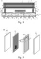
- the chip package structure 100 includes a first chip 2, a conductive pillar 6, and a second chip 4.
- the first chip 2 and the second chip 4 may have different functions.
- the first chip 2 may be a controller
- the second chip 4 may be a memory chip.
- the memory chip has a memory structure for providing a storage function.
- the memory chip includes but are not limited to a Nand chip, a resistive memory chip, and a dynamic random-access memory.
- the first chip 2 may also be a memory chip
- the second chip 4 may also be a controller, which is not limited in the embodiments of the present disclosure.
- the chip package structure 100 further includes a package substrate 1.
- the package substrate 1 is rigid and thus may provide support for the first chip 2, the conductive pillar 6, and the second chip 4. A reference may be made to the following descriptions for the conductive pillar 6, which is not explained herein.
- the package substrate 1 includes a plurality of dielectric layers 11 and a plurality of metal wiring layers 12, which are alternately disposed.
- One metal wiring layer 12 is disposed between two adjacent dielectric layers 11, and one dielectric layer 11 is disposed between two adjacent metal wiring layers 12.
- Each metal wiring layer 12 includes a metal line, and the metal lines in two adjacent metal wiring layers 12 may run through the dielectric layer 11 between the two metal wiring layers 12 and be connected as required.
- the dielectric layer 11 in the package substrate 1 is formed by a spin coating process
- the metal wiring layer 12 in the package substrate 1 is formed by a physical vapor deposition (PVD) process in combination with an electroplating process. Therefore, compared with a package substrate formed by a press-fit process, the package substrate 1 constituted by the dielectric layer 11 and the metal wiring layer 12, provided by the embodiments of the present disclosure, has a smaller thickness, a smaller spacing between the adjacent metal wiring layers 12, and thus a higher integration rate of the metal lines in the metal wiring layer 12.
- the number of metal wiring layers 12 may be 4 or 5.
- FIG. 4 illustrates 4 metal wiring layers 12.
- the dielectric layer 11 may be made from, for example, an insulating resin material, which for example, includes but is not limited to polybenzoxazole (PBO), polyimide (PI), and the like.
- PBO polybenzoxazole
- PI polyimide
- the metal wiring layer 12 may be made from, for example, a conductive material, which for example, includes but is not limited to gold, silver, copper, aluminum, and the like.
- the package substrate 1 may further include a solder resist layer 13.
- the number of solder resist layers 13 may be two.
- the plurality of dielectric layers 11 and the plurality of metal wiring layers 12 form a stacked structure, and the two solder resist layers 13 are located on the front side and the back side of the stacked structure respectively.
- the solder resist layer 13 may not only play the role of insulation, but also protect the package substrate 1 and prevents the metal lines in the package substrate 1 from being oxidized.
- the solder resist layer 13 may be made from an organic material, for example, a solder resist ink, as long as it can play the role of insulation, which is not limited in the embodiments of the present disclosure.
- the package substrate 1 has a first surface A and a second surface B that are opposite to each other.
- the first surface is an upper surface of the package substrate shown in FIG. 4 and the second surface is a lower surface of the package substrate shown in FIG. 4 .
- the first surface A of the package substrate 1 is provided with a first pad 14 and a second pad 15 disposed at an interval. There may be a plurality of first pads 14 and a plurality of second pads 15. FIG. 4 illustrates nine first pads 14 and two second pads 15.
- both of the first pads 14 and the second pads 15 are located in the uppermost metal wiring layer 12 of the package substrate 1.
- the solder resist layer 13 is also provided with a plurality of vias, each of which exposes one first pad 14 or one second pad 15.
- the first chip 2 is located on the first surface A of the package substrate 1 and electrically connected to the package substrate 1.
- the first chip 2 is electrically connected to the first pad 14 on the package substrate 1.
- the first chip 2 may be disposed in the middle of the package substrate 1, and accordingly, each first pad 14 may be located in the middle of the package substrate 1.
- the first chip 2 and the first pad 14 may be electrically connected by a soldering process.
- the soldering process may be a hot pressure soldering process, an ultrasonic pressure soldering process or a thermosonic soldering process.
- the first chip 2 and the first pad 14 may also be electrically connected by other means, which is not limited in the embodiments of the present disclosure.
- the chip package structure 100 further includes a conductive pillar 6.
- the conductive pillar 6 is located on the first surface A of the package substrate 1 and electrically connected to the package substrate 1.
- the conductive pillar 6 is electrically connected to the second pad 15 on the package substrate 1.
- the conductive pillar 6 may be made of at least one of metal copper, metal aluminum, metal silver, or tin.
- the conductive pillar 6 may be columnar, such as cylindrical and prismatic.
- the conductive pillar 6 may also be in other irregular shapes, which is not limited in the embodiments of the present disclosure.
- the second chip 4 is located on the side of the first chip 2 and the conductive pillar 6 away from the package substrate 1.
- the second chip 4 is electrically connected to the conductive pillar 6 and is not in direct electrical connection with the first chip 2.
- the electrical connection between the second chip 4 and the conductive pillar 6 may be realized in various ways.
- the second chip 4 may be electrically connected to the conductive pillar 6 by means of flip-chip bonding.
- flip-chip bonding refers to a process of forming bumps on a connect pad of a chip and directly connecting the bumps to a PCB substrate or a metal substrate.
- the second chip 4 and the conductive pillar 6 are electrically connected by means of flip-chip bonding, which means that bumps are formed on a connect pad of the second chip 4 and directly connected to the conductive pillar 6.
- the second chip 4 includes a body 40 and a pin 41 located below the body 40.
- the chip package structure 100 further includes a first pad 61 located between the pin 41 and the conductive pillar 6.
- the second chip 4 is electrically connected to the conductive pillar 6 by the first pad 61.
- the pin 41 refers to the connect pad
- the first pad 61 refers to the bump.
- the pin 41 may be made from at least one of copper, titanium, nickel, tungsten and silver for example.
- the first pad 61 may be made from tin for example.
- the second chip 4 may be electrically connected to the conductive pillar 6 by a soldering process.
- the soldering process may be a hot pressure soldering method, an ultrasonic pressure soldering method, a thermosonic soldering process, or the like.
- an orthographic projection of the conductive pillar 6 on the package substrate 1 is located within an orthographic projection of the first chip 2 or the second chip 4 on the package substrate 1.
- the second chip 4 may completely cover the conductive pillar 6, and the conductive pillar 6 is located within the boundary of the orthographic projection of the second chip 4 on the package substrate 1.
- the conductive pillar 6 may provide support for the second chip 4, so as to improve the stability of the second chip 4 and further improve the structure stability of the chip package structure 100.
- the conductive pillar 6 Since the conductive pillar 6 is located below the second chip 4 and electrically connected to a surface on a side of the second chip 4 close to the package substrate 1, the conductive pillar 6 may extend in a direction perpendicular to the first surface A of the package substrate 1 to be in a vertical state.
- the length of a path of signal transmission between the second chip 4 and the package substrate 1 substantially equals the height of the conductive pillar 6, or, substantially equals the distance between the first surface A and the surface on the side of the second chip 4 close to the package substrate 1. In this way, the path of signal transmission between the first chip 2 and the second chip 4 can be greatly shortened and the rate of signal transmission can be greatly improved.
- the cross-sectional area of the conductive pillar 6 is larger than that of the gold wire, and correspondingly, the resistance of the conductive pillar 6 is lower than that of the gold wire, which helps to further improve the rate of signal transmission.
- the orthographic projection of the conductive pillar 6 on the package substrate 1 may also be located within the orthographic projection of the first chip 2 on the package substrate 1.
- the area of the orthographic projection of the first chip 2 on the package substrate 1 may be greater than the area of the orthographic projection of the second chip 4 on the package substrate 1, and the conductive pillar 6 may be electrically connected to the second chip 4 after running through the first chip 2.
- the second chip 4 is placed above the first chip 2, such that the package substrate 1, the first chip 2, the conductive pillar 6 and the second chip 4 form a stacked structure, which improves the compactness of the chip package structure 100 and helps to reduce the area of the chip package structure 100.
- the orthographic projection of the conductive pillar 6 on the package substrate 1 is located within the range of the orthographic projection of the first chip 2 or the second chip 4 on the package substrate 1. In this way, the space around the first chip 2 or the second chip 4 may not be occupied, which helps to further miniaturize the chip package structure 100 and to further reduce the area of the chip package structure 100.
- the effective length of the conductive pillar 6 substantially equals the distance between the first surface A and the surface on the side of the second chip 4 close to the package substrate 1.
- the path of signal transmission between the first chip 2 and the second chip 4 in the embodiment of the present application is shortened, which helps to improve the rate of signal transmission.
- the conductive pillar 6 is larger in size and lower in resistance, which helps to further improve the rate of signal transmission between the first chip 2 and the second chip 4. Accordingly, the chip package structure 100 can be improved in response speed and reduced in power consumption, and electricity can be saved.
- the size of the package plane is approximate to the size of the area of the second chip, for example.
- a surface on a side of the second chip 4 close to the package substrate 1 is higher than a surface on a side of the first chip 2 away from the package substrate 1, with respect to the first surface A of the package substrate 1. That is, there is a certain distance between the surface on the side of the second chip 4 close to the package substrate 1 and the surface on the side of the first chip 2 away from the package substrate 1. That is, the first chip 2 and the second chip 4 are disposed at intervals in a direction perpendicular to the first surface A.
- the distance between the surface on the side of the second chip 4 close to the package substrate 1 and the surface on the side of the first chip 2 away from the package substrate 1 is greater than or equal to 20 ⁇ m.
- the distance may be 20 ⁇ m, 30 ⁇ m, 40 ⁇ m, 50 ⁇ m, 60 ⁇ m, 70 ⁇ m, etc.
- the “distance” herein refers to a distance in a direction perpendicular to the first surface.
- ends of the conductive pillars 6 away from the package substrate 1 are higher than the surface on the side of the first chip 2 away from the package substrate 1.
- the distance between the surface on the side of the second chip 4 close to the package substrate 1 and the first surface A of the package substrate 1 is h1
- the distance between the surface on the side of the first chip 2 away from the package substrate 1 and the first surface A of the package substrate 1 is h2
- h1 and h2 meet: 5 8 ⁇ h 2 h 1 ⁇ 4 5 .
- a value of h 2 h 1 may be, for example, 5 8 , 5 7 , 7 10 , 3 4 , 4 5 , etc.
- the distance between the surface on the side of the first chip 2 away from the package substrate 1 and the first surface A of the package substrate 1 ranges from 50 ⁇ m to 80 ⁇ m.
- the distance between the surface on the side of the second chip 4 close to the package substrate 1 and the first surface A of the package substrate 1 may be 70 ⁇ m to 110 ⁇ m.
- the distance between the surface on the side of the second chip 4 close to the package substrate 1 and the first surface A of the package substrate 1 may be 70 ⁇ m.
- the distance between the surface on the side of the first chip 2 away from the package substrate 1 and the first surface A of the package substrate 1 is 80 ⁇ m
- the distance between the surface on the side of the second chip 4 close to the package substrate 1 and the first surface A of the package substrate 1 may be 110 ⁇ m.
- the distance between the first chip 2 and the second chip 4 can also be prevented from being too large, which ensures a thin and light structure of the chip package structure 100.
- a number of conductive pillars 6 is greater than one.
- the plurality of conductive pillars 6 are at least located on two opposite sides of the first chip 2.
- the plurality of conductive pillars 6 are located on two opposite sides of the first chip 2 (as shown in Fig. 2 ); or the plurality of conductive pillars 6 are located on three or four sides of the first chip 2 (as shown in Fig. 3 ).
- the number of the conductive pillars 6 located on different sides of the first chip 2 may be the same or different.
- the plurality of conductive pillars 6 located on the same side of the first chip 2 may be regularly arranged in at least one column; of course, the plurality of conductive pillars 6 located on the same side of the first chip 2 may also be disposed in a staggered way, which is not limited by the embodiment of the present disclosure.
- the plurality of conductive pillars 6 are at least disposed on two opposite sides of the first chip 2, which can not only ensure electrical connection between the second chip 4 and the package substrate 1, but also provide a relatively balanced supporting force for the second chip 4 and ensure structure stability of the second chip 4.
- the chip package structure 100 further includes a package layer 7.
- the package layer 7 is located between the package substrate 1 and the second chip 4, covers the first chip 2, and surrounds sides of the conductive pillars 6.
- the package layer 7 is a whole layer structure, a surface on a side of the package layer 7 away from the package substrate 1 is, for example, a flat surface, this surface is, for example, flush with the surfaces on the side of the conductive pillars away from the package substrate 1, and the package layer 7 exposes the surfaces on the side of the conductive pillars 6 away from the package substrate 1.
- the area of an orthographic projection of the package layer 7 on the package substrate 1 is basically coincident with the area of the first surface A of the package substrate 1; and a boundary of the orthographic projection of the package layer 7 on the package substrate 1 is basically coincident with a boundary of the first surface A of the package substrate 1.
- a material of the package layer 7 may be a molding compand material. At this point, the package layer 7 may be formed by a molding process. The material of the package layer 7 may also be other materials, which is not limited by the embodiment of the present disclosure.
- the package layer 7 is in contact with the sides of the conductive pillars 6 to provide physical protection for the first chip 2 and the conductive pillars 6, and to fix the positions of the first chip 2 and the conductive pillars 6 on the package substrate, which ensures structure integrity and stability of the chip package structure 100.
- the orthographic projection of the second chip 4 on the package substrate 1 is located within the range of the orthographic projection of the package layer 7 on the package substrate 1.
- an area of the orthographic projection of the second chip 4 on the package substrate 1 is less than an area of the orthographic projection of the package layer 7 on the package substrate 1.
- a boundary of the orthographic projection of the package layer 7 on the package substrate 1 surrounds a boundary of the orthographic projection of the second chip 4 on the package substrate 1, and there is a certain distance between the two boundaries.
- the package layer 7 can provide certain support for the second chip 4.
- the chip package structure 100 further includes a first filling portion 8. At least part of the first filling portion 8 is located between the package layer 7 and the second chip 4, and the first filling portion 8 surrounds each pin of the second chip 4.
- the first filling portion 8 is located between the package layer 7 and the second chip 4, and the second chip 4 covers the first filling portion 8.
- the first filling portion 8 is located not only between the package layer 7 and the second chip 4, but also on both sides of the second chip 4, and the orthographic projection of the second chip 4 on the package substrate 1 is located within the range of an orthographic projection of the first filling portion 8 on the package substrate 1.
- the first filling portion 8 is filled between any two adjacent pins of the second chip 4, so as to avoid short circuit between the two adjacent pins.
- a material of the first filling portion 8 may be an epoxy resin material or the like.
- the epoxy resin material or the like is filled between the package layer 7 and the second chip 4 to form the first filling portion 8, a hole may be formed, and an area of the hole is, for example, less than or equal to 15%.
- the first filling portion 8 between the package layer 7 and the second chip 4 not only can the support be provided for the second chip 4, but also the bonding force between the second chip 4 and the package layer 7 is enhanced, and the structure stability of the second chip 4 is ensured, thereby improving the reliability of the chip package structure 100.
- the short circuit between any two adjacent pins of the second chip 4 can also be avoided, which ensures a yield of the chip package structure 100.
- the chip package structure 100 further includes an electromagnetic shielding layer 9.
- the electromagnetic shielding layer 9 at least covers the second chip 4 as well as the sides of the package layer 7.
- the electromagnetic shielding layer 9 covers the second chip 4 as well as the sides of the package layer 7.
- the electromagnetic shielding layer 9 covers not only the second chip 4 as well as the sides of the package layer 7, but also other components, for example, the electromagnetic shielding layer 9 also covers the sides of the first filling portion 8, etc., which is not limited by the embodiment of the present disclosure.
- the electromagnetic shielding layer 9 is made of a ferromagnetic material (such as steel) with a very high magnetic permeability, and the electromagnetic shielding layer 9 may electromagnetically shield a covered region thereof.
- the electromagnetic shielding layer 9 By disposing the electromagnetic shielding layer 9, the first chip 2 and the second chip 4 can be effectively prevented from being subjected to electromagnetic interference, thereby improving an anti-electromagnetic interference capability of the chip package structure 100.
- the package substrate 1 further includes at least one ground wire 16.
- the ground wire 16 is located on the metal wiring layer 12.
- the electromagnetic shielding layer 9 also covers the sides of the package substrate 1, and is electrically connected to the ground wire 16.
- the electromagnetic shielding layer 9 covers the second chip 4 as well as the sides of the package layer 7 and the sides of the package substrate 1 to electromagnetically shield the chip package structure 100 and effectively prevent the electromagnetic interference. Furthermore, the electromagnetic shielding layer 9 is further electrically connected to the ground wire 16, and can lead electromagnetic radiation out through grounding, which realizes double anti-electromagnetic interference and further ensures efficient operation of the chip package structure 100. At this point, the anti-electromagnetic interference capability of the chip package structure 100 is realized by the electromagnetic shielding layer 9, which is low in process cost, simple and convenient to implement and suitable for mass production.
- the second chip 4 includes a plurality of sub-chips 42.
- the plurality of sub-chips 42 are sequentially stacked in a direction perpendicular to the package substrate 1 and away from the package substrate 1.
- types of the plurality of sub-chips are the same, and optionally, the sub-chips are all memory chips.
- an isolation structure 43 is disposed between two adjacent sub-chips 42.
- a material of the isolation structure 43 may be an adhesive material. Two adjacent sub-chips 42 are connected by the adhesive material.
- one sub-chip 42 close to the package substrate 1 in the plurality of sub-chips 42 is electrically connected to the conductive pillar 6, thereby realizing electrical connection with the package substrate 1 through the conductive pillar.
- Other sub-chips 42 are electrically connected to the package substrate 1 through a wire by a wire bonding process.
- each sub-chip 42 is respectively electrically connected to the package substrate 1, so that each sub-chip 42 respectively communicates with the first chip 2. At this point, each sub-chip 42 can store different information under control of the first chip 2, which ensures storage diversity of the chip package structure 100.
- two adjacent sub-chips 42 are electrically connected.
- two adjacent sub-chips 42 may be connected to each other by a gold wire.
- the sub-chip 42 includes a sub-pin 401, and the chip package structure 100 further includes a second pad 402 located between two adjacent sub-chips 42. As shown in Fig. 6 , two adjacent sub-chips 42 are electrically connected through the pin and the second pad 402.
- a material of the sub-pin 401 includes at least one of metal copper, titanium, nickel, tungsten and silver.
- a material of the second pad 402 may include tin.
- two adjacent sub-chips 42 may be electrically connected by a soldering process.
- the soldering process may be a hot-press soldering method, an ultrasonic pressure soldering method, a thermal ultrasonic soldering method or the like.
- an integration degree of the chip package structure 100 can be improved and product performances of the chip package structure 100 can be improved on the basis of ensuring a smaller package area.
- the first chip 2 may also include a plurality of sub-chips.
- the plurality of sub-chips may be sequentially stacked in a direction away from the package substrate 1.
- the chip package structure 100 further includes a second filling portion 10. At least part of the second filling portion 10 is located between the package substrate 1 and the first chip 2, and the second filling portion 10 surrounds each pin of the first chip 2.
- the second filling portion 10 is located between the package substrate 1 and the first chip 2, and the first chip 2 covers the second filling portion 10.
- the second filling portion 10 is located not only between the package substrate 1 and the first chip 2, but also on both sides of the first chip 2, and the orthographic projection of the first chip 2 on the package substrate 1 is located within the range of an orthographic projection of the second filling portion 10 on the package substrate 1.
- the second filling portion 10 is filled between any two adjacent pins of the first chip 2, so as to avoid short circuit between the two adjacent pins.
- a material of the second filling portion 10 is an epoxy resin material or the like.
- a hole may be formed, and an area of the hole is , for example, less than or equal to 15%.
- the second filling portion 10 between the package substrate 1 and the first chip 2 not only can the support be provided for the first chip 2, but also the bonding force between the first chip 2 and the package substrate 1 is enhanced, and structure stability of the first chip 2 is ensured, thereby improving the reliability of the chip package structure 100.
- the short circuit between any two adjacent pins of the first chip 2 can also be avoided, which ensures the yield of the chip package structure 100.
- the second surface B of the package substrate 1 is provided with third pads 17.
- the third pads 17 are located on the metal wiring layers 12. For example, a number of third pads 17 is greater than one.
- solder resist layers 13 are provided with a plurality of vias, and each via exposes one third pad 17.
- the chip package structure 100 further includes solder balls 20.
- a number of solder balls 20 is greater than one, and the plurality of solder balls 20 are located on the second surface B of the package substrate 1 and electrically connected to the package substrate 1.
- solder balls 20 are electrically connected to the third pads 17 on the package substrate 1.
- the plurality of solder balls 20 and the plurality of third pads 17 may be disposed in one-to-one correspondence.
- solder balls 20 may be soldered on the third pads 17 by a ball planting process.
- solder balls 20 are electrically connected to the metal wires in the package substrate 1 through the third pads 17. At this point, the solder ball 20 may serve as an interface between the package substrate 1 and outside world, which realizes electrical connection between the chip package structure 100 and an external module, and further realizes communication between the chip package structure 100 and the external module.
- the pins (i.e., input/output (I/O) terminals) of the first chip 2 are redistributed through the package substrate 1 and the plurality of solder balls 20 located on the second surface B of the package substrate 1.
- the chip package structure 100 is a fan-out chip package structure, and the fan-out chip package structure is connected to the external module (such as a motherboard or a printed circuit board) through the solder balls 20.
- the embodiment of the present disclosure also provides another chip package structure 100.
- the chip package structure 100 includes the first chip 2 and a second chipset 44.
- the second chipset 44 includes a plurality of second chips 4.
- the plurality of second chips 4 are, for example, sequentially stacked in the direction perpendicular to the package substrate 1 and away from the package substrate 1.
- the first chip 2 and the second chip 4 may have different functions.
- the first chip 2 may be a controller and the second chip 4 may be a memory chip.
- the memory chip has a memory structure for providing a memory function.
- the memory chip includes but not limited to a Nand chip, a resistive memory chip, a dynamic random-access memory and the like.
- the first chip 2 may also be the memory chip, and the second chip 4 may be the controller, which are not limited by the embodiment of the present disclosure.
- the chip package structure 100 further includes the package substrate 1.
- the package substrate 1 is rigid, and thus can provide support for the first chip 2 and the second chip 4.
- the package substrate 1 includes a plurality of dielectric layers 11 and a plurality of metal wiring layers 12, which are alternately disposed.
- One metal wiring layer 12 is disposed between two adjacent dielectric layers 11, and one dielectric layer 11 is disposed between two adjacent metal wiring layers 12.
- Each metal wiring layer 12 includes a metal line, and the metal lines in two adjacent metal wiring layers 12 may run through the dielectric layer 11 between the two metal wiring layers 12 and be connected as required.
- the dielectric layer 11 in the package substrate 1 is formed by a spin coating process
- the metal wiring layer 12 in the package substrate 1 is formed by a physical vapor deposition (PVD) process in combination with an electroplating process. Therefore, compared with a package substrate formed by a press-fit process, the package substrate 1 constituted by the dielectric layer 11 and the metal wiring layer 12, provided by the embodiments of the present disclosure, has a smaller thickness, a smaller spacing between the adjacent metal wiring layers 12, and thus a higher integration rate of the metal lines in the metal wiring layer 12.
- the number of metal wiring layers 12 may be 4 or 5.
- FIG. 7 illustrates 4 metal wiring layers 12.
- the dielectric layer 11 may be made from, for example, an insulating resin material, which for example, includes but is not limited to polybenzoxazole (PBO), polyimide (PI), and the like.
- PBO polybenzoxazole
- PI polyimide
- the metal wiring layer 12 may be made from, for example, a conductive material, which for example, includes but is not limited to gold, silver, copper, aluminum, and the like.
- the package substrate 1 may further include a solder resist layer 13.
- the number of solder resist layers 13 may be two.
- the plurality of dielectric layers 11 and the plurality of metal wiring layers 12 form a stacked structure, and the two solder resist layers 13 are located on the front side and the back side of the stacked structure respectively.
- the solder resist layer 13 may not only play the role of insulation, but also protect the package substrate 1 and prevents the metal lines in the package substrate 1 from being oxidized.
- the solder resist layer 13 may be made from an organic material, for example, a solder resist ink, as long as it can play the role of insulation, which is not limited in the embodiments of the present disclosure.
- the package substrate 1 has a first surface A and a second surface B that are opposite to each other.
- the first surface is an upper surface of the package substrate shown in FIG. 7 and 8 and the second surface is a lower surface of the package substrate shown in FIG. 7 and 8 .
- the first surface A of the package substrate 1 is provided with a first pad 14 and a second pad 15 disposed at an interval. There may be a plurality of first pads 14 and a plurality of second pads 15. FIG. 8 illustrates nine first pads 14 and two second pads 15.
- both of the first pads 14 and the second pads 15 are located in the uppermost metal wiring layer 12 of the package substrate 1.
- the solder resist layer 13 is also provided with a plurality of vias, each of which exposes one first pad 14 or one second pad 15.
- the first chip 2 is located on the first surface A of the package substrate 1 and electrically connected to the package substrate 1.
- the first chip 2 is electrically connected to the first pad 14 on the package substrate 1.
- the first chip 2 and the first pad 14 may be electrically connected by a soldering process.
- the soldering process may be a hot pressure soldering process, an ultrasonic pressure soldering process or a thermosonic soldering process.
- the first chip 2 and the first pad 14 may also be electrically connected by other means, which is not limited in the embodiments of the present disclosure.
- the second chipset 44 is located on a side of the first chip 2 away from the package substrate 1.
- the second chipset 44 is electrically connected to the package substrate 1, and has no direct electrical connection with the first chip 2.
- the second chipset 44 and the package substrate 1 may be electrically connected in various ways.
- the second chipset 44 and the package substrate 1 may be electrically connected through conductive structures 30.
- the conductive structures 30 are electrically connected to the package substrate 1 and the second chipset 44.
- the conductive structures 30 may include wires 31. Ends of the wires 31 are electrically connected to the second chipset 44, and the other ends of the wires 31 are electrically connected to the exposed metal wiring layers 12 on the package substrate 1, so that the second chipset 44 is electrically connected to the package substrate 1 by bonding leads to the wires 31.
- a material of the wires may include at least one of metal gold, metal aluminum, metal silver or metal copper.
- the shape of the conductive structure 30 may be columnar, for example, cylindrical, prismatic, etc.
- the shape of the conductive pillar 6 may also be other irregular shapes, which is not limited by the embodiment of the present disclosure.
- the material of the conductive structure 30 may include at least one of metal copper, metal aluminum, metal silver or tin.
- the second chipset 44 is placed above the first chip 2, so that the package substrate 1, the first chip 2 and the second chipset 44 form a stacked structure, which improves the compactness of the chip package structure 100 and helps to reducing the area of the chip package structure 100. Furthermore, by stacking the plurality of second chips 4 to form the second chipset 44, the integration degree of the chip package structure 100 can be improved and the product performances of the chip package structure 100 can be improved on the basis of ensuring a smaller package area.
- the isolation structure 43 is disposed between two adjacent second chips 4.
- the material of the isolation structures 43 may be an adhesive material. Two adjacent second chips 4 are connected by the adhesive material.
- two adjacent second chips 4 are electrically connected. Two adjacent second chips 4 may be electrically connected in various ways.
- two adjacent second chips 4 may be connected to each other by a wire.
- the material of the wire may include at least one of metal gold, metal aluminum, metal silver or metal copper.
- the second chip 4 has a through silicon via (TSV), and the TSV is filled with a conductive material.
- the chip package structure 100 further includes a third pad 431 located between two adjacent second chips 4. As shown in Fig. 8 , the conductive metal at the TSV and the third pad 431 may be electrically connected by a soldering process, thereby realizing electrical connection between two connected second chips 4.
- the second chip 4 may include a body and pins located below the body.
- the chip package structure 100 further includes pads located on the pins and another second chip 4.
- the second chip 4 is electrically connected to another second chip 4 through the pads.
- the plurality of second chips 4 can be directly connected to each other, which shortens the signal transmission path between adjacent second chips 4 and improving the signal transmission speed.
- each second chip 4 is electrically connected to the package substrate 1 through the wire 31.
- each second chip 4 is respectively electrically connected to the package substrate 1, so that each second chip 4 respectively communicates with the first chip 2. At this point, each second chip 4 can store different information under control of the first chip 2, which ensures storage diversity of the chip package structure 100.
- the plurality of first chips 2 may be sequentially stacked in the direction away from the package substrate 1.
- a surface on a side of the second chipset 44 close to the package substrate 1 is higher than a surface on a side of the first chip 2 away from the package substrate 1. That is, there is a certain distance between the surface on the side of the second chipset 44 close to the package substrate 1 and the surface on the side of the first chip 2 away from the package substrate 1. That is, in the direction perpendicular to the first surface A, the first chip 2 and the second chipset 44 are disposed at intervals.
- the distance between the surface on the side of the second chipset 44 close to the package substrate 1 and the surface on the side of the first chip 2 away from the package substrate 1 is greater than or equal to 20 ⁇ m.
- the distance may be 20 ⁇ m, 30 ⁇ m, 40 ⁇ m, 50 ⁇ m, 60 ⁇ m, 70 ⁇ m, etc.
- the “distance” here refers to the distance in the direction perpendicular to the first surface.
- the distance between the surface on the side of the second chipset 44 close to the package substrate 1 and the first surface A of the package substrate 1 is h1
- the distance between the surface on the side of the first chip 2 away from the package substrate 1 and the first surface A of the package substrate 1 is h2
- h1 and h2 meet: 5 8 ⁇ h 2 h 1 ⁇ 4 5 .
- a value of h 2 h 1 may be, for example, 5 8 , 5 7 , 7 10 , 3 4 , 4 5 , etc.
- the distance between the surface on the side of the first chip 2 away from the package substrate 1 and the first surface A of the package substrate 1 ranges from 50 ⁇ m to 80 ⁇ m.
- the distance between the surface on the side of the second chipset 44 close to the package substrate 1 and the first surface A of the package substrate 1 may be 70 ⁇ m to 110 ⁇ m.
- the distance between the surface on the side of the second chipset 44 close to the package substrate 1 and the first surface A of the package substrate 1 may be 70 ⁇ m.
- the distance between the surface on the side of the first chip 2 away from the package substrate 1 and the first surface A of the package substrate 1 is 80 ⁇ m
- the distance between the surface on the side of the second chipset 44 close to the package substrate 1 and the first surface A of the package substrate 1 may be 110 ⁇ m.
- the distance between the first chip 2 and the second chipset 44 can be prevented from being too large, which ensures the thin and light structure of the chip package structure 100.
- the chip package structure 100 further includes the package layer 7.
- the package layer 7 is located between the package substrate 1 and the second chipset 44, and the package layer 7 covers the first chip 2.
- the package layer 7 is a whole layer structure, and the surface on the side of the package layer 7 away from the package substrate 1 is, for example, a flat surface.
- the surface on the side of the package layer 7 away from the package substrate 1 is, for example, flush with the surface on the side of the conductive structure 30 away from the package substrate 1, and the package layer 7 exposes the surface on the side of the conductive structure 30 away from the package substrate 1.
- the area of the orthographic projection of the package layer 7 on the package substrate 1 is basically consistent with the area of the first surface A of the package substrate 1; and the boundary of the orthographic projection of the package layer 7 on the package substrate 1 is basically coincident with the boundary of the first surface A of the package substrate 1.
- the material of the package layer 7 may be a molding compand material. At this point, the package layer 7 may be formed by a molding process. The material of the package layer 7 may also be other materials, which is not limited by the embodiment of the present disclosure.
- the first chip 2 can be packaged by the package layer 7, but also the first chip 2 can be physically protected by the package layer 7, and the position of the first chip 2 on the package substrate can be fixed to ensure the structure integrity and stability of the chip package structure 100.
- an orthographic projection of the second chipset 44 on the package substrate 1 is located within the range of the orthographic projection of the package layer 7 on the package substrate 1.
- the area of the orthographic projection of the second chipset 44 on the package substrate 1 is less than the area of the orthographic projection of the package layer 7 on the package substrate 1.
- the boundary of the orthographic projection of the package layer 7 on the package substrate 1 surrounds a boundary of the orthographic projection of the second chipset 44 on the package substrate 1, and there is a certain distance between the two boundaries.
- the package layer 7 can provide certain support for the second chipset 44.
- the chip package structure 100 further includes the first filling portion 8. At least part of the first filling portion 8 is located between the package layer 7 and the second chipset 44, and the first filling portion 8 surrounds each pin of one second chip 4 close to the package substrate 1.
- the first filling portion 8 is located between the package layer 7 and the second chipset 44, and the second chipset 44 covers the first filling portion 8.
- the first filling portion 8 is located not only between the package layer 7 and the second chipset 44, but also on both sides of one second chip 4 close to the package substrate 1, and an orthographic projection of one second chip 4 close to the package substrate 1 on the package substrate 1 is located within the range of an orthographic projection of the first filling portion 8 on the package substrate 1.
- the first filling portion 8 is filled between any two adjacent pins of one second chip 4 close to the package substrate 1 to avoid short circuit between the two adjacent pins.
- a material of the first filling portion 8 may be an epoxy resin material or the like.
- the epoxy resin material or the like is filled between the package layer 7 and the second chipset 44 to form the first filling portion 8, a hole may be formed, and the area of the hole is, for example, less than or equal to 15%.
- the first filling portion 8 between the package layer 7 and the second chipset 44, not only can the support be provided for the second chipset 44, but also the bonding force between the second chipset 44 and the package layer 7 is enhanced, and structure stability of the second chipset 44 is ensured, thereby improving the reliability of the chip package structure 100.
- the short circuit between any two adjacent pins of one second chip 4 close to the package substrate 1 can also be avoided, thereby ensuring the yield of the chip package structure 100.
- the chip package structure 100 further includes the electromagnetic shielding layer 9.
- the electromagnetic shielding layer 9 at least covers the second chipset 44 as well as sides of the package layer 7.
- the electromagnetic shielding layer 9 covers the second chipset 44 as well as sides of the package layer 7.
- the electromagnetic shielding layer 9 covers not only the second chipset 44 as well as sides of the package layer 7, but also other components, for example, the electromagnetic shielding layer 9 also covers sides of the first filling portion 8, etc., which is not limited by the embodiment of the present disclosure.
- the electromagnetic shielding layer 9 is made of a ferromagnetic material (such as steel) with a very high magnetic permeability, and the electromagnetic shielding layer 9 may electromagnetically shield a covered region thereof.
- the electromagnetic shielding layer 9 By disposing the electromagnetic shielding layer 9, the first chip 2 and the second chipset 44 can be effectively prevented from being subjected to electromagnetic interference, thereby improving the anti-electromagnetic interference capability of the chip package structure 100.
- the package substrate 1 further includes at least one ground wire 16.
- the ground wire 16 is located on the metal wiring layer 12.
- the electromagnetic shielding layer 9 also covers the sides of the package substrate 1, and is electrically connected to the ground wire 16.
- the electromagnetic shielding layer 9 covers the second chipset 44 and the sides of the package layer 7 as well as the sides of the package substrate 1 to electromagnetically shield the chip package structure 100 and effectively prevent electromagnetic interference. Furthermore, the electromagnetic shielding layer 9 is electrically connected to the ground wire 16, and can lead electromagnetic radiation out through grounding, which realizes double anti-electromagnetic interference and ensures the efficient operation of the chip package structure 100. At this point, the anti-electromagnetic interference capability of the chip package structure 100 is realized by the electromagnetic shielding layer 9, which is low in process cost, simple and convenient to implement and suitable for mass production.
- the chip package structure 100 further includes the second filling portion 10. At least part of the second filling portion 10 is located between the package substrate 1 and the first chip 2, and the second filling portion 10 surrounds each pin of the first chip 2.
- the second filling portion 10 is located between the package substrate 1 and the first chip 2, and the first chip 2 covers the second filling portion 10.
- the second filling portion 10 is located not only between the package substrate 1 and the first chip 2, but also on both sides of the first chip 2, and an orthographic projection of the first chip 2 on the package substrate 1 is located within the range of an orthographic projection of the second filling portion 10 on the package substrate 1.
- the second filling portion 10 is filled between any two adjacent pins of the first chip 2, so as to avoid short circuit between the two adjacent pins.
- the material of the second filling portion 10 is an epoxy resin material or the like.
- a hole may be formed, and the area of the hole is, for example, less than or equal to 15%.
- the second filling portion 10 between the package substrate 1 and the first chip 2 not only can the support be provided for the first chip 2, but also the bonding force between the first chip 2 and the package substrate 1 is enhanced, and the structure stability of the first chip 2 is ensured, thereby improving the reliability of the chip package structure 100.
- the short circuit between any two adjacent pins of the first chip 2 can also be avoided, which ensures the yield of the chip package structure 100.
- third pads 17 are disposed on the second surface B of the package substrate 1.
- the third pads 17 are located on the metal wiring layers 12. For example, a number of third pads 17 is greater than one.
- the solder resist layer 13 is provided with a plurality of vias, and each via exposes one third pad 17.
- the chip package structure 100 further includes the solder balls 20.
- a number of solder balls 20 is greater than one, and the plurality of solder balls 20 are located on the second surface B of the package substrate 1 and electrically connected to the package substrate 1.
- solder balls 20 are electrically connected to the third pads 17 on the package substrate 1.
- the plurality of solder balls 20 and the plurality of third pads 17 may be disposed in one-to-one correspondence.
- solder balls 20 may be soldered on the third pads 17 by a ball planting process.
- solder balls 20 are electrically connected to the metal wires in the package substrate 1 through the third pads 17. At this point, the solder balls 20 may serve as an interface between the package substrate 1 and the outside world, which realizes the electrical connection between the chip package structure 100 and the external module, and further realizes the communication between the chip package structure 100 and the external module.
- the signal transmission path between the solder balls 20 and the metal wires in the package substrate 1 is shortened, and the signal transmission speed is improved.
- the pins (i.e., input/output (I/O) terminals) of the first chip 2 are redistributed through the package substrate 1 and the plurality of solder balls 20 located on the second surface B of the package substrate 1.
- the chip package structure 100 is a fan-out chip package structure, and the fan-out chip package structure is connected to the external module (such as a motherboard or a printed circuit board) through the solder balls 20.
- the embodiment of the present disclosure also provides an electronic device 1000.
- the electronic device 1000 includes the chip package structure 100 according to some above embodiments.
- the electronic device may further include a cover plate 200, a display screen 300, a middle frame 400, and a back shell 500.
- the display screen 300 may be a liquid crystal display (LCD) screen, and may also be an organic light emitting diode (OLED) display screen, a quantum dot light emitting diode (QLED) display screen, a mini light emitting diode (Mini LED) display screen or a micro light emitting diode (Micro LED) display screen, etc.
- OLED organic light emitting diode
- QLED quantum dot light emitting diode
- Mini LED mini light emitting diode
- Micro LED micro light emitting diode
- the OLED display screen, QLED display screen, Mini LED display screen and Micro LED display screen are all self-luminous display screens.
- the middle frame 400 may include a carrier plate 410 and a frame 420.
- the electronic device 1000 may further include a circuit board 600 disposed on the carrier plate 410.
- the chip package structure 100 is disposed on the circuit board 600 and electrically connected to the circuit board 600.
- the beneficial effects that can be achieved by the electronic device according to the present disclosure can refer to the above beneficial effects of the semiconductor structure, which will not be repeated here.
- the above electronic device may be any one of a mobile phone, a desktop computer, a tablet computer, a notebook computer, a server, a vehicle-mounted device, a wearable device (such as a smart watch, a smart bracelet and smart glasses), a mobile power supply, a game machine, a digital multimedia player, etc.
- Fig. 10 is a flowchart of a manufacturing method of a chip package structure according to some embodiments of the present disclosure.
- Figs. 11A to 11E , 12A to 12C , 13A to 13C , and 14A to 14C are respectively structure cross-sectional diagrams corresponding to steps in the manufacturing method of a chip package structure according to some embodiments. It should be understood that the steps shown in Fig. 10 are not exclusive, and other steps may be executed before, after or between any shown steps. In addition, some of these steps may be executed simultaneously, or may be executed in an order different from that shown in Fig. 10 .
- the above manufacturing method includes the following steps S1 to S4.
- the structure of the package substrate 1 may refer to the illustrations in some above embodiments, which will not be repeated here.
- the conductive pillars 6 are formed on the first surface A of the package substrate 1, and the conductive pillars 6 are electrically connected to the package substrate 1.
- the conductive pillars 6 may be formed by a sputtering process or an electroplating process.
- the material of the conductive pillars 6 may include at least one of copper, aluminum, silver or tin.
- the first chip 2 is disposed on the first surface A of the package substrate 1.
- the first chip 2 is electrically connected to the package substrate 1.
- connection way of the first chip 2 and the package substrate 1 may refer to the illustrations in some above embodiments, which will not be repeated here.
- the second chip 4 is disposed on a side of the conductive pillars 6 and the first chip 2 away from the package substrate 1.
- the second chip 4 is electrically connected to the conductive pillars 6.
- the orthographic projections of the conductive pillars 6 on the package substrate 1 are located within the orthographic projection of the first chip 2 or the second chip 4 on the package substrate 1.
- the manufacturing method disclosed in the above embodiment of the present disclosure has the same structure and beneficial effects as the chip package structure 100 according to some above embodiments, which will not be repeated here.
- steps of the above manufacturing method may be executed simultaneously, or may be executed in an order different from that shown in Fig. 10 .
- the above steps S2 and S3 may be reversed, that is, the first chip 2 is firstly disposed on the first surface A of the package substrate 1, and then the conductive pillars 6 are formed on the first surface A of the package substrate 1.
- the above manufacturing method further includes: S10 to S20.
- a package film 07 is formed on the first chip 2 and the conductive pillars 6, and the package film 07 covers the first chip 2 and the conductive pillars 6.
- the embodiment of the present disclosure may use chemical vapor deposition (CVD) or physical vapor deposition (PVD) to form the package film 07.
- a thickness of the package film is greater than the height of the conductive pillar and the thickness of the first chip, that is, relative to the package substrate, the surface on the side of the package film away from the package substrate is higher than the surface on the side of the conductive pillar away from the package substrate and higher than the surface on the side of the first chip away from the package substrate.
- the package film 07 is thinned to expose the conductive pillars 6, and the remaining package film 07 forms the package layer 7; the package layer 7 covers the first chip 2.
- the package film 07 may be thinned by mechanical polishing, chemical mechanical planarization, wet etching and other thinning processes.
- the height of the conductive pillars 6 may also be lowered to ensure that the conductive pillars 6 are exposed, thereby improving an electrical connection yield between the conductive pillars 6 and the second chip 4.
- the package film 07 covering the first chip 2 and the conductive pillars 6 may be formed by a molding material through a molding process.
- the above step S2 includes: S21 to S23.
- the package layer 7 is formed on the first chip 2, and the package layer 7 covers the first chip 2.
- the covering package layer 7 may be formed by the molding material through the molding process.
- vias 71 are formed in the package layer 7, and the vias 71 expose the second pads 15.
- the vias 71 may be formed through an etching process.
- the shape of the vias 71 may be columnar, for example, cylindrical and the like.
- the shape of the vias 71 may also be other irregular shapes, which is not limited by the embodiment of the present disclosure.
- the material of the conductive pillars 6 may be tin or the like.
- solder balls may be filled in the vias and reflowed to form solder pillars, which are the above conductive pillars 6.
- the above manufacturing method further includes: filling a first insulating material between the package layer 7 and the second chip 4 to form the first filling portion 8, and the first filling portion 8 surrounds each pin of the second chip 4.
- the first filling portion 8 is located between the package layer 7 and the second chip 4, and the second chip 4 covers the first filling portion 8.
- the first filling portion 8 is located not only between the package layer 7 and the second chip 4, but also on both sides of the second chip 4, and the orthographic projection of the second chip 4 on the package substrate 1 is located within the range of the orthographic projection of the first filling portion 8 on the package substrate 1.
- the first filling portion 8 is filled between any two adjacent pins of the second chip 4, so as to avoid short circuit between the two adjacent pins.
- the first insulating material may be an epoxy resin material or the like.
- the first filling portion 8 between the package layer 7 and the second chip 4 not only can the support be provided for the second chip 4, but also the bonding force between the second chip 4 and the package layer 7 is enhanced, which ensures the structure stability of the second chip 4, and also avoids short circuit between any two adjacent pins of the second chip 4, thereby further ensuring the yield of the chip package structure 100.
- the above manufacturing method further includes: forming the electromagnetic shielding layer 9, and the electromagnetic shielding layer 9 at least covers the second chip 4 as well as the sides of the package layer 7, as shown in Fig. 11E .
- the electromagnetic shielding layer 9 is made of a ferromagnetic material (such as steel) with a very high magnetic permeability, and the electromagnetic shielding layer 9 may electromagnetically shield a covered region thereof.
- the electromagnetic shielding layer 9 may be formed on the second chip 4 as well as the sides of the package layer 7 by means of spraying, electroplating, vacuum sputtering or the like.
- the ferromagnetic material may be sprayed on the second chip 4 as well as the sides of the package layer 7 to form the electromagnetic shielding layer 9.
- the second chip 4 includes a plurality of sub-chips 42.
- the above step S4 includes: S41 to S42.
- the plurality of sub-chips 42 are stacked in sequence along the direction perpendicular to the package substrate 1 and away from the package substrate 1.
- the types of the plurality of sub-chips are the same, and optionally, the plurality of sub-chips are all memory chips.
- an isolation structure 43 is disposed between two adjacent sub-chips 42.
- the material of the isolation structure 43 may be an adhesive material. Two adjacent sub-chips 42 are stacked by the adhesive material.
- connection relationships of the plurality of sub-chips 42 there may be a plurality of connection relationships of the plurality of sub-chips 42, and the details may refer to the illustrations in some above embodiments, and will not be repeated here.
- the electromagnetic shielding layer 9 may be formed, and the electromagnetic shielding layer 9 at least covers the plurality of sub-chips 42 and the sides of the package layer 7.
- the integration degree of the chip package structure 100 can be improved and the product performances of the chip package structure 100 can be improved on the basis of ensuring a small package volume.
- the above manufacturing method further includes: filling a second insulating material between the package substrate 1 and the first chip 2 to form the second filling portion 10, and the second filling portion 10 surrounds each pin of the first chip 2, as shown in Fig. 11C .
- the second filling portion 10 is filled between any two adjacent pins of the first chip 2, so as to avoid short circuit between the two adjacent pins.
- the second insulating material may be an epoxy resin material or the like.
- the second filling portion 10 between the package substrate 1 and the first chip 2 not only can the support be provided for the first chip 2, but also the bonding force between the first chip 2 and the package substrate 1 is improved, and the structure stability of the first chip 2 is ensured.
- the short circuit between any two adjacent pins of the first chip 2 can also be avoided, which ensures the yield of the chip package structure 100.
- third pads 17 are disposed on the second surface B of the package substrate 1.
- the first surface A and the second surface B are opposite to each other.
- the above manufacturing method further includes: forming the solder balls 20 on the second surface B of the package substrate 1, and the solder balls 20 are electrically connected to the third pads 17, as shown in Fig. 11D .
- solder balls 20 may be soldered on the third pads 17 by a ball planting process.
- a number of solder balls 20 is greater than one, the plurality of solder balls 20 may form a ball grid array (BGA), and the ball grid array may serve as an interface between the chip package structure 100 and the outside world.
- BGA ball grid array
Landscapes
- Structures Or Materials For Encapsulating Or Coating Semiconductor Devices Or Solid State Devices (AREA)
- Semiconductor Integrated Circuits (AREA)
- Engineering & Computer Science (AREA)
- Manufacturing & Machinery (AREA)
- Physics & Mathematics (AREA)
- Health & Medical Sciences (AREA)
- Electromagnetism (AREA)
- Toxicology (AREA)
- Wire Bonding (AREA)
- Internal Circuitry In Semiconductor Integrated Circuit Devices (AREA)
Abstract
Description
- The present disclosure relates to the field of semiconductor technologies, and particularly relates to a chip package structure, a manufacturing method thereof, and an electronic device.
- With the rapid development of wireless communication, automotive electronics and other consumer electronics, electronic devices have a trend of development towards multi-functionality. Therefore, in manufacturing these electronic devices, chips with different functions are usually packaged separately and then integrated, and the integrated components are disposed inside the electronic devices.
- Package is an important step in the manufacturing process of the electronic devices. However, the chips in the prior art are prone to the problems of large size and relatively low rate of signal transmission after being packaged.
- Embodiments of the present disclosure provide a chip package structure, a manufacturing method thereof, and an electronic device, for the purposes of reducing the area of the chip package structure and improving the rate of signal transmission.
- To fulfill the above objects, the embodiments of the present disclosure have the following technical solutions.
- In an aspect, a chip package structure is provided. The chip package structure includes a package substrate, a first chip, a conductive pillar and a second chip, wherein the package substrate has a first surface; the first chip is located on the first surface of the package substrate and electrically connected to the package substrate; the conductive pillar is located on the first surface of the package substrate and electrically connected to the package substrate; the second chip is located on a side of the first chip and the conductive pillar away from the package substrate and electrically connected to the conductive pillar; and an orthographic projection of the conductive pillar on the package substrate is located within a range of an orthographic projection of the first chip or the second chip on the package substrate.
- In the chip package structure according to the foregoing embodiment of the present disclosure, the second chip is placed above the first chip, such that the package substrate, the first chip, the conductive pillar and the second chip form a stacked structure, which improves the compactness of the chip package structure and helps to reduce the area of the chip package structure. Moreover, the conductive pillar is provided to realize the electrical connection between the second chip and the package substrate, and the conductive pillar is disposed under the
first chip 2 or the second chip such that the orthographic projection of the conductive pillar on the package substrate is located within the range of the orthographic projection of thefirst chip 2 or the second chip on the package substrate. In this way, the space around thefirst chip 2 or the second chip may not be occupied, which helps to further miniaturize the chip package structure and to further reduce the area of the chip package structure. - In some embodiments, an orthographic projection of the conductive pillar on the package substrate is also located within a range of an orthographic projection of the first chip on the package substrate.
- In some embodiments, the chip package structure further includes a package layer, and the package layer is located between the package substrate and the second chip, covers the first chip and surrounds sides of the conductive pillar.
- In some embodiments, an orthographic projection of the second chip on the package substrate is located within a range of an orthographic projection of the package layer on the package substrate.
- In some embodiments, the chip package structure further includes a first filling portion, and at least part of the first filling portion is located between the package layer and the second chip and the first filling portion surrounds each pin of the second chip.
- In some embodiments, the chip package structure further includes an electromagnetic shielding layer, and the electromagnetic shielding layer at least covers the second chip as well as sides of the package layer.
- In some embodiments, the package substrate further includes at least one ground wire, and the electromagnetic shielding layer also covers sides of the package substrate and is electrically connected to the ground wire.
- In some embodiments, the second chip comprises a plurality of sub-chips sequentially stacked in a direction perpendicular to and away from the package substrate.
- In some embodiments, two adjacent sub-chips are electrically connected to each other.
- In some embodiments, one of the plurality of sub-chips close to the package substrate is electrically connected to the conductive pillar, and others of the plurality of sub-chips are electrically connected to the package substrate by a wire.
- In some embodiments, a surface on a side of the second chip close to the package substrate is higher than a surface on a side of the first chip away from the package substrate, with respect to the first surface of the package substrate.
- In some embodiments, a distance between the surface on the side of the second chip close to the package substrate and the first surface of the package substrate is h1, a distance between the surface on the side of the first chip away from the package substrate and the first surface of the package substrate is h2, and h1 and h2 meet the following condition:

- In some embodiments, a number of the conductive pillars is greater than one, and the plurality of conductive pillars are at least located on two opposite sides of the first chip.
- In some embodiments, the chip package structure further includes a second filling portion, and at least part of the second filling portion is located between the package substrate and the first chip and the second filling portion surrounds each pin of the first chip.
- In some embodiments, the package substrate has a second surface opposite to the first surface, and the chip package structure further comprises a solder ball located on the second surface of the package surface and electrically connected to the package substrate.
- In another aspect, another chip package structure is provided. The chip package structure includes: a package substrate having a first surface; a first chip disposed on the first surface of the package substrate and electrically connected to the package substrate; and a second chipset located on a side of the first chip away from the package substrate, electrically connected to the package substrate, and comprising a plurality of second chips sequentially stacked in a direction perpendicular to and away from the package substrate.
- In some embodiments, two adjacent second chips are electrically connected to each other.
- In some embodiments, each of the plurality of second chips is electrically connected to the package substrate by a wire.
- In some embodiments, the chip package structure further includes a package layer, and the package layer is located between the package substrate and the second chipset and covers the first chip.
- In some embodiments, an orthographic projection of the second chipset on the package substrate is located within a range of an orthographic projection of the package layer on the package substrate.
- In some embodiments, the chip package structure further includes a first filling portion, and at least part of the first filling portion is located between the package layer and the second chipset and the first filling portion surrounds each pin of one second chip close to the package substrate.
- In some embodiments, the chip package structure further includes an electromagnetic shielding layer, the electromagnetic shielding layer at least covers the second chipset as well as sides of the package layer.
- In some embodiments, the package substrate includes at least one ground wire, and the electromagnetic shielding layer also covers sides of the package substrate and is electrically connected to the ground wire.
- In some embodiments, a surface on a side of the second chipset close to the package substrate is higher than a surface on a side of the first chip away from the package substrate, with respect to the first surface of the package substrate.
- In some embodiments, a distance between the surface on the side of the second chipset close to the package substrate and the first surface of the package substrate is h1, a distance between the surface on the side of the first chip away from the package substrate and the first surface of the package substrate is h2, and h1 and h2 meet the following condition:

- In some embodiments, the chip package structure further includes a second filling portion, and at least part of the second filling portion is located between the package substrate and the first chip and the second filling portion surrounds each pin of the first chip.
- In some embodiments, the package substrate has a second surface opposite to the first surface, and the chip package structure further comprises a solder ball located on the second surface of the package surface and electrically connected to the package substrate.
- In yet another aspect, an electronic device is provided. The electronic device includes the chip package structure as described in some embodiments above.
- In still another aspect, a manufacturing method of a chip package structure is provided. The manufacturing method includes: providing a package substrate having a first surface on which a first pad and a second pad are disposed at an interval; forming a conductive pillar on the first surface of the package structure, the conductive pillar being electrically connected to the second pad; disposing a first chip on the first surface of the package substrate, the first chip being electrically connected to the first pad; and disposing a second chip on a side of the conductive pillar and the first chip away from the package substrate, the second chip being electrically connected to the conductive pillar, an orthographic projection of the conductive pillar on the package substrate being located within a range of an orthographic projection of the second chip on the package substrate.
- In some embodiments, before the disposing the second chip on the side of the conductive pillar and the first chip away from the package substrate, the manufacturing method further comprises: forming a package film on the first chip and the conductive pillar, the package film covering the first chip and the conductive pillar; and thinning the package film to expose the conductive pillar and to obtain a package layer, the package layer covering the first chip.
- In some embodiments, the forming the conductive pillar on the first surface of the package substrate comprises: forming a package layer on the first chip, the package layer covering the first chip; forming a via in the package layer, the via exposing a second pad; and filling the via with a conductive material to form the conductive pillar.
- In some embodiments, the manufacturing method further includes: filling a first insulating material between the package layer and the second chip to form a first filling portion, the first filling portion surrounding each pin of the second chip.
- In some embodiments, the manufacturing method further includes: forming an electromagnetic shielding layer, the electromagnetic shielding layer at least covering the second chip as well as sides of the package layer.
- In some embodiments, the second chip comprises a plurality of sub-chips; and the disposing the second chip on the side of the conductive pillar and the first chip away from the package substrate comprises: sequentially stacking the plurality of sub-chips in a thickness direction of the sub-chips to form the second chip; and soldering the second chip with an end of the conductive pillar away from the package substrate, such that the second chip is electrically connected to the conductive pillar.
- In some embodiments, after disposing the first chip and before disposing the second chip, the manufacturing method further includes: filling a second insulating material between the package substrate and the first chip to form a second filling portion, the second filling portion surrounding each pin of the first chip.
- In some embodiments, a third pad is disposed on a second surface of the package substrate, and the first surface and the second surface are opposite to each other; and before or after forming the package layer, the manufacturing method further includes: forming a solder ball on the second surface of the package substrate, the solder ball being electrically connected to the third pad.
- It can be understood that for the beneficial effects of the electronic device and the manufacturing method of the chip package structure provided by the foregoing embodiments of the present disclosure, a reference may be made to the beneficial effects of the chip package structure described above, which will not be repeated herein.
- For clearer descriptions of the technical solutions in the present disclosure, a brief introduction may be given hereinafter to the accompany drawings that may be used in some embodiments of the present disclosure. Apparently, the drawings in the following descriptions are merely for illustrating some embodiments of the present disclosure, and other drawings may be obtained by those of ordinary skill in the art according to these drawings. In addition, the drawings in the following descriptions may be considered as schematic diagrams but not a limitation to the product actual size, the method actual flow, etc. related to the embodiments of the present disclosure.
-
FIG. 1 is a schematic structure diagram of a chip package structure according to some embodiments; -
FIG. 2 is a top view of a chip package structure according to some embodiments; -
FIG. 3 is a top view of another chip package structure according to some embodiments; -
FIG. 4 is a sectional structure diagram of the chip package structure shown inFIG. 2 in a B-B' direction; -
FIG. 5 is a sectional structure diagram of the chip package structure shown inFIG. 2 in a D-D' direction; -
FIG. 6 is another sectional structure diagram of the chip package structure shown inFIG. 2 in the B-B' direction; -
FIG. 7 is a schematic structure diagram of yet another chip package structure according to some embodiments; -
FIG. 8 is a schematic structure diagram of still another chip package structure according to some embodiments; -
FIG. 9 is a schematic structure diagram of an electronic device according to some embodiments; -
FIG. 10 is a flow chart of a manufacturing method of a chip package structure according to some embodiments; -
FIGS. 11A to 11E are structure diagrams corresponding to steps in a manufacturing method of a chip package structure according to some embodiments; -
FIGS. 12A to 12C are structure diagrams corresponding to steps of a manufacturing method of a conductive pillar according to some embodiments; -
FIGS. 13A to 13C are structure diagrams corresponding to steps of another manufacturing method of a conductive pillar according to some embodiments; and -
FIGS. 14A to 14C are structure diagrams corresponding to steps of a manufacturing method of a second chip according to some embodiments. - The technical solutions in some embodiments of the present disclosure will be described clearly and completely below with reference to the accompanying drawings. Apparently, the described embodiments are only a part of embodiments of the present disclosure, rather than all of the embodiments. All other embodiments obtained by those of ordinary skill in the art based on the embodiments provided by the present disclosure shall fall within the scope of protection of the present disclosure.
- In the descriptions of the present disclosure, it should be understood that directional or positional relationships indicated by the terms such as "center", "upper", "lower", "front", "back ", "left", "right", "vertical", "horizontal", "top", "bottom", "inner", and "outer" are directional or positional relationships as shown in the drawings, only for the purposes of the ease in describing the present disclosure and simplification of its descriptions, but not indicating or implying that the specified apparatus or element has to be located in a specific direction, and structured and operated in a specific direction, and therefore, should not be understood as limitations to the present disclosure.
- Unless the context otherwise requires, throughout the description and claims, the term "comprise" is interpreted as an open-ended inclusion, i.e., "comprising, but not limited to". In the descriptions, the terms "an embodiment", "some embodiments", "exemplary embodiments", "exemplarily" or "some examples", etc. are intended to indicate that a specific feature, structure, material or characteristic related to the embodiment or example is included in at least one embodiment or example of the present disclosure. Schematic representations of the above terms do not necessarily refer to the same embodiment or example. In addition, the specific feature, structure, material or characteristic described may be included in any one or more embodiments or examples in any appropriate manner.
- Hereinafter, the terms "first" and "second" are only intended for description and shall not be construed to indicate or imply relative importance, or imply the number of the indicated technical features. Therefore, the features defined by "first" and "second" can indicate or imply that one or more features are included. In the descriptions of the embodiments of the present disclosure, unless otherwise stated, "a plurality of" means two or more.
- In describing some embodiments, the expressions of "connect" and its extensions may be used. For example, some embodiments may be described by using the term "connect" to indicate that two or more components are in direct physical or electrical contact. For another example, some embodiments may be described by using the term "couple" to indicate that two or more components are in direct physical contact or electrical contact. However, the term "couple" may also mean that two or more components are not in direct contact but still cooperate or interact with each other. The embodiments disclosed herein are not necessarily limited to the content herein.
- "At least one of A, B and C" and "at least one of A, B or C" have the same meaning of including the following combinations of A, B and C: only A, only B, only C, a combination of A and B, a combination of A and C, a combination of B and C, and a combination of A, B and C.
- "A and/or B" includes the following three combinations: only A, only B, and a combination of A and B.
- In addition, the use of "based on" means openness and inclusiveness, because the process, step, calculation or other actions "based on" one or more conditions or values can be based on additional conditions or beyond the values in practice.
- In the present disclosure, the meaning of "on," "above," and "over" should be interpreted in the broadest manner such that "on" not only means "directly on" something but also includes the meaning of "on" something with an intermediate feature or a layer therebetween, and that "above" or "over" not only means the meaning of "above" or " over" something but can also include the meaning it is "above" or "over" something with no intermediate feature or layer therebetween (i.e., directly on something).
- The disclosure describes exemplary embodiments with reference to sectional views and/or planar views as idealized illustrative drawings. In the drawings, the thicknesses of layers and areas are enlarged for clarity. It is thus conceivable of the change in shape with respect to the drawings due to, for example, manufacturing techniques and/or tolerances. Therefore, the exemplary embodiments should not be interpreted to be limited to the shape of the area shown herein, but to include the shape deviation due to, for example, manufacturing. For example, an etched area shown as a rectangle will generally have a curved feature. Therefore, the areas shown in the drawings are schematic in nature, and their shapes are neither intended to show the actual shape of the area of the device, nor intended to limit the scope of the exemplary embodiments.
- In an implementation , as shown in
FIG. 1 , a first chip 2' and a second chip 3' in a chip package structure 100' are typically disposed side by side on a package substrate 1' in a tiling manner. - A plurality of gold fingers are disposed on a side of the package substrate 1' close to the first chip 2' and the second chip 3'. The first chip 2' and the second chip 3' are respectively connected to the gold fingers by gold wires 4' by using the WB (wire bonding) process, so that the first chip 2' and the second chip 3' may be electrically connected by the respectively connected gold wires 4' and the package substrate 1', thereby realizing communication between the first chip 2' and the second chip 3'.
- However, the first chip 2' and the second chip 3' are disposed side by side, which makes the area of the chip package structure 100' larger. Moreover, due to the wire arcs of the gold wires 4' and the existence of the gold fingers, it is necessary to reserve certain areas around the first chip 2' and the second chip 3', which further increases the area of the chip package structure 100'. Generally, the area of the chip package structure 100' obtained after the first chip 2' and the second chip 3' are packaged is increased by at least 30% compared with the sum of the areas of the first chip 2' and the second chip 3'. In addition, due to large lengths and high resistance of the gold wires 4', the rate of signal transmission may be low in the process of transmitting a signal between the first chip 2' and the second chip 3' through the different gold wires 4'.
- Accordingly, in some embodiments of the present disclosure, a
chip package structure 100 is provided. There may be various types ofchip package structures 100, such as an embedded multi-media card (EMMC), a universal flash storage (UFS) and a multi-chip package (MCP). As shown inFIGS. 2, 3 , and4 , thechip package structure 100 includes afirst chip 2, aconductive pillar 6, and asecond chip 4. - The
first chip 2 and thesecond chip 4 may have different functions. For example, thefirst chip 2 may be a controller, and thesecond chip 4 may be a memory chip. The memory chip has a memory structure for providing a storage function. There may be various types of memory chips. For example, the memory chip includes but are not limited to a Nand chip, a resistive memory chip, and a dynamic random-access memory. Of course, thefirst chip 2 may also be a memory chip, and thesecond chip 4 may also be a controller, which is not limited in the embodiments of the present disclosure. - In some examples, the
chip package structure 100 further includes apackage substrate 1. Thepackage substrate 1 is rigid and thus may provide support for thefirst chip 2, theconductive pillar 6, and thesecond chip 4. A reference may be made to the following descriptions for theconductive pillar 6, which is not explained herein. - Exemplarily, as shown in
FIG. 4 , thepackage substrate 1 includes a plurality ofdielectric layers 11 and a plurality of metal wiring layers 12, which are alternately disposed. Onemetal wiring layer 12 is disposed between two adjacent dielectric layers 11, and onedielectric layer 11 is disposed between two adjacent metal wiring layers 12. Eachmetal wiring layer 12 includes a metal line, and the metal lines in two adjacent metal wiring layers 12 may run through thedielectric layer 11 between the two metal wiring layers 12 and be connected as required. - In some examples, the
dielectric layer 11 in thepackage substrate 1 is formed by a spin coating process, and themetal wiring layer 12 in thepackage substrate 1 is formed by a physical vapor deposition (PVD) process in combination with an electroplating process. Therefore, compared with a package substrate formed by a press-fit process, thepackage substrate 1 constituted by thedielectric layer 11 and themetal wiring layer 12, provided by the embodiments of the present disclosure, has a smaller thickness, a smaller spacing between the adjacent metal wiring layers 12, and thus a higher integration rate of the metal lines in themetal wiring layer 12. - Optionally, The number of metal wiring layers 12 may be 4 or 5.
FIG. 4 illustrates 4 metal wiring layers 12. - The
dielectric layer 11 may be made from, for example, an insulating resin material, which for example, includes but is not limited to polybenzoxazole (PBO), polyimide (PI), and the like. - The
metal wiring layer 12 may be made from, for example, a conductive material, which for example, includes but is not limited to gold, silver, copper, aluminum, and the like. - Exemplarily, as shown in
FIG. 4 , thepackage substrate 1 may further include a solder resistlayer 13. For example, the number of solder resistlayers 13 may be two. The plurality ofdielectric layers 11 and the plurality of metal wiring layers 12 form a stacked structure, and the two solder resistlayers 13 are located on the front side and the back side of the stacked structure respectively. - The solder resist
layer 13 may not only play the role of insulation, but also protect thepackage substrate 1 and prevents the metal lines in thepackage substrate 1 from being oxidized. - Optionally, the solder resist
layer 13 may be made from an organic material, for example, a solder resist ink, as long as it can play the role of insulation, which is not limited in the embodiments of the present disclosure. - In some examples, as shown in
FIG. 4 , thepackage substrate 1 has a first surface A and a second surface B that are opposite to each other. The first surface is an upper surface of the package substrate shown inFIG. 4 and the second surface is a lower surface of the package substrate shown inFIG. 4 . - As shown in
FIG. 4 , the first surface A of thepackage substrate 1 is provided with afirst pad 14 and asecond pad 15 disposed at an interval. There may be a plurality offirst pads 14 and a plurality ofsecond pads 15.FIG. 4 illustrates ninefirst pads 14 and twosecond pads 15. - Exemplarily, both of the
first pads 14 and thesecond pads 15 are located in the uppermostmetal wiring layer 12 of thepackage substrate 1. The solder resistlayer 13 is also provided with a plurality of vias, each of which exposes onefirst pad 14 or onesecond pad 15. - In some examples, as shown in
FIG. 4 , thefirst chip 2 is located on the first surface A of thepackage substrate 1 and electrically connected to thepackage substrate 1. - Optionally, the
first chip 2 is electrically connected to thefirst pad 14 on thepackage substrate 1. - Exemplarily, in the top views shown in
FIGS. 2 and 3 , thefirst chip 2 may be disposed in the middle of thepackage substrate 1, and accordingly, eachfirst pad 14 may be located in the middle of thepackage substrate 1. Thefirst chip 2 and thefirst pad 14 may be electrically connected by a soldering process. For example, the soldering process may be a hot pressure soldering process, an ultrasonic pressure soldering process or a thermosonic soldering process. Of course, thefirst chip 2 and thefirst pad 14 may also be electrically connected by other means, which is not limited in the embodiments of the present disclosure. - In some examples, as shown in
FIG. 4 , thechip package structure 100 further includes aconductive pillar 6. Theconductive pillar 6 is located on the first surface A of thepackage substrate 1 and electrically connected to thepackage substrate 1. - Optionally, the
conductive pillar 6 is electrically connected to thesecond pad 15 on thepackage substrate 1. - Exemplarily, the
conductive pillar 6 may be made of at least one of metal copper, metal aluminum, metal silver, or tin. - Exemplarily, the
conductive pillar 6 may be columnar, such as cylindrical and prismatic. Of course, theconductive pillar 6 may also be in other irregular shapes, which is not limited in the embodiments of the present disclosure. - In some examples, as shown in
FIG. 4 , thesecond chip 4 is located on the side of thefirst chip 2 and theconductive pillar 6 away from thepackage substrate 1. Thesecond chip 4 is electrically connected to theconductive pillar 6 and is not in direct electrical connection with thefirst chip 2. - The electrical connection between the
second chip 4 and theconductive pillar 6 may be realized in various ways. For example, in an embodiment of the present disclosure, thesecond chip 4 may be electrically connected to theconductive pillar 6 by means of flip-chip bonding. - It can be understood that flip-chip bonding refers to a process of forming bumps on a connect pad of a chip and directly connecting the bumps to a PCB substrate or a metal substrate. Specifically, in an embodiment of the present disclosure, the
second chip 4 and theconductive pillar 6 are electrically connected by means of flip-chip bonding, which means that bumps are formed on a connect pad of thesecond chip 4 and directly connected to theconductive pillar 6. - Exemplarily, as shown in
FIG. 4 , thesecond chip 4 includes abody 40 and a pin 41 located below thebody 40. At this time, thechip package structure 100 further includes afirst pad 61 located between the pin 41 and theconductive pillar 6. Thesecond chip 4 is electrically connected to theconductive pillar 6 by thefirst pad 61. For example, the pin 41 refers to the connect pad, and thefirst pad 61 refers to the bump. - The pin 41 may be made from at least one of copper, titanium, nickel, tungsten and silver for example. The
first pad 61 may be made from tin for example. Thesecond chip 4 may be electrically connected to theconductive pillar 6 by a soldering process. Exemplarily, the soldering process may be a hot pressure soldering method, an ultrasonic pressure soldering method, a thermosonic soldering process, or the like. - Exemplarily, an orthographic projection of the
conductive pillar 6 on thepackage substrate 1 is located within an orthographic projection of thefirst chip 2 or thesecond chip 4 on thepackage substrate 1. For example, it can be seen fromFIGS 2 and 3 that thesecond chip 4 may completely cover theconductive pillar 6, and theconductive pillar 6 is located within the boundary of the orthographic projection of thesecond chip 4 on thepackage substrate 1. - In the case that the orthographic projection of the
conductive pillar 6 on thepackage substrate 1 is located within the orthographic projection of thesecond chip 4 on thepackage substrate 1, theconductive pillar 6 may provide support for thesecond chip 4, so as to improve the stability of thesecond chip 4 and further improve the structure stability of thechip package structure 100. - Since the
conductive pillar 6 is located below thesecond chip 4 and electrically connected to a surface on a side of thesecond chip 4 close to thepackage substrate 1, theconductive pillar 6 may extend in a direction perpendicular to the first surface A of thepackage substrate 1 to be in a vertical state. The length of a path of signal transmission between thesecond chip 4 and thepackage substrate 1 substantially equals the height of theconductive pillar 6, or, substantially equals the distance between the first surface A and the surface on the side of thesecond chip 4 close to thepackage substrate 1. In this way, the path of signal transmission between thefirst chip 2 and thesecond chip 4 can be greatly shortened and the rate of signal transmission can be greatly improved. - In addition, the cross-sectional area of the
conductive pillar 6 is larger than that of the gold wire, and correspondingly, the resistance of theconductive pillar 6 is lower than that of the gold wire, which helps to further improve the rate of signal transmission. - In the case that the orthographic projection of the
conductive pillar 6 on thepackage substrate 1 is located within the orthographic projection of thefirst chip 2 on thepackage substrate 1, the orthographic projection of theconductive pillar 6 on thepackage substrate 1 may also be located within the orthographic projection of thefirst chip 2 on thepackage substrate 1. At this time, the area of the orthographic projection of thefirst chip 2 on thepackage substrate 1 may be greater than the area of the orthographic projection of thesecond chip 4 on thepackage substrate 1, and theconductive pillar 6 may be electrically connected to thesecond chip 4 after running through thefirst chip 2. - Therefore, in the
chip package structure 100 according to some embodiments of the present disclosure, thesecond chip 4 is placed above thefirst chip 2, such that thepackage substrate 1, thefirst chip 2, theconductive pillar 6 and thesecond chip 4 form a stacked structure, which improves the compactness of thechip package structure 100 and helps to reduce the area of thechip package structure 100. Moreover, by providing theconductive pillar 6 to realize the electrical connection between thesecond chip 4 and thepackage substrate 1, and by disposing theconductive pillar 6 below thefirst chip 2 or thesecond chip 4, the orthographic projection of theconductive pillar 6 on thepackage substrate 1 is located within the range of the orthographic projection of thefirst chip 2 or thesecond chip 4 on thepackage substrate 1. In this way, the space around thefirst chip 2 or thesecond chip 4 may not be occupied, which helps to further miniaturize thechip package structure 100 and to further reduce the area of thechip package structure 100. - In addition, the effective length of the
conductive pillar 6 substantially equals the distance between the first surface A and the surface on the side of thesecond chip 4 close to thepackage substrate 1. Compared with the electrical connection between thesecond chip 4 and thepackage substrate 1 realized by the gold wires, the path of signal transmission between thefirst chip 2 and thesecond chip 4 in the embodiment of the present application is shortened, which helps to improve the rate of signal transmission. Moreover, compared with the gold wire, theconductive pillar 6 is larger in size and lower in resistance, which helps to further improve the rate of signal transmission between thefirst chip 2 and thesecond chip 4. Accordingly, thechip package structure 100 can be improved in response speed and reduced in power consumption, and electricity can be saved. - It should be noted that in the case the area of the second chip is larger than that of the first chip, in the chip package structure, the size of the package plane is approximate to the size of the area of the second chip, for example.
- In some embodiments, as shown in
FIG. 4 , a surface on a side of thesecond chip 4 close to thepackage substrate 1 is higher than a surface on a side of thefirst chip 2 away from thepackage substrate 1, with respect to the first surface A of thepackage substrate 1. That is, there is a certain distance between the surface on the side of thesecond chip 4 close to thepackage substrate 1 and the surface on the side of thefirst chip 2 away from thepackage substrate 1. That is, thefirst chip 2 and thesecond chip 4 are disposed at intervals in a direction perpendicular to the first surface A. - Exemplarily, the distance between the surface on the side of the
second chip 4 close to thepackage substrate 1 and the surface on the side of thefirst chip 2 away from thepackage substrate 1 is greater than or equal to 20 µm. For example, the distance may be 20 µm, 30 µm, 40 µm, 50 µm, 60 µm, 70 µm, etc. The "distance" herein refers to a distance in a direction perpendicular to the first surface. - With the above arrangement, signal interference between the
second chip 4 and thefirst chip 2 can be avoided, which helps to improve the reliability and reliability of thechip package structure 100. - Optionally, relative to the first surface A of the
package substrate 1, ends of theconductive pillars 6 away from thepackage substrate 1 are higher than the surface on the side of thefirst chip 2 away from thepackage substrate 1. - In some embodiments, as shown in
Fig. 4 , the distance between the surface on the side of thesecond chip 4 close to thepackage substrate 1 and the first surface A of thepackage substrate 1 is h1, the distance between the surface on the side of thefirst chip 2 away from thepackage substrate 1 and the first surface A of thepackage substrate 1 is h2, and h1 and h2 meet:

- Exemplarily, a value of


- In some examples, the distance between the surface on the side of the
first chip 2 away from thepackage substrate 1 and the first surface A of thepackage substrate 1 ranges from 50 µm to 80 µm. At this point, the distance between the surface on the side of thesecond chip 4 close to thepackage substrate 1 and the first surface A of thepackage substrate 1 may be 70 µm to 110 µm. For example, when the distance between the surface on the side of thefirst chip 2 away from thepackage substrate 1 and the first surface A of thepackage substrate 1 is 50 µm, the distance between the surface on the side of thesecond chip 4 close to thepackage substrate 1 and the first surface A of thepackage substrate 1 may be 70 µm. For another example, when the distance between the surface on the side of thefirst chip 2 away from thepackage substrate 1 and the first surface A of thepackage substrate 1 is 80 µm, the distance between the surface on the side of thesecond chip 4 close to thepackage substrate 1 and the first surface A of thepackage substrate 1 may be 110 µm. - With the above arrangement, a certain distance can be ensured between the
first chip 2 and thesecond chip 4, thereby avoiding signal interference between thefirst chip 2 and thesecond chip 4. On this basis, the distance between thefirst chip 2 and thesecond chip 4 can also be prevented from being too large, which ensures a thin and light structure of thechip package structure 100. - In some embodiments, as shown in
Fig. 2 and Fig. 3 , a number ofconductive pillars 6 is greater than one. The plurality ofconductive pillars 6 are at least located on two opposite sides of thefirst chip 2. Exemplarily, the plurality ofconductive pillars 6 are located on two opposite sides of the first chip 2 (as shown inFig. 2 ); or the plurality ofconductive pillars 6 are located on three or four sides of the first chip 2 (as shown inFig. 3 ). - Exemplarily, the number of the
conductive pillars 6 located on different sides of thefirst chip 2 may be the same or different. The plurality ofconductive pillars 6 located on the same side of thefirst chip 2 may be regularly arranged in at least one column; of course, the plurality ofconductive pillars 6 located on the same side of thefirst chip 2 may also be disposed in a staggered way, which is not limited by the embodiment of the present disclosure. - In the present embodiment, the plurality of
conductive pillars 6 are at least disposed on two opposite sides of thefirst chip 2, which can not only ensure electrical connection between thesecond chip 4 and thepackage substrate 1, but also provide a relatively balanced supporting force for thesecond chip 4 and ensure structure stability of thesecond chip 4. - In some embodiments, as shown in
Fig. 5 andFig. 6 , thechip package structure 100 further includes apackage layer 7. Thepackage layer 7 is located between thepackage substrate 1 and thesecond chip 4, covers thefirst chip 2, and surrounds sides of theconductive pillars 6. - Exemplarily, the
package layer 7 is a whole layer structure, a surface on a side of thepackage layer 7 away from thepackage substrate 1 is, for example, a flat surface, this surface is, for example, flush with the surfaces on the side of the conductive pillars away from thepackage substrate 1, and thepackage layer 7 exposes the surfaces on the side of theconductive pillars 6 away from thepackage substrate 1. - Exemplarily, the area of an orthographic projection of the
package layer 7 on thepackage substrate 1 is basically coincident with the area of the first surface A of thepackage substrate 1; and a boundary of the orthographic projection of thepackage layer 7 on thepackage substrate 1 is basically coincident with a boundary of the first surface A of thepackage substrate 1. - Exemplarily, a material of the
package layer 7 may be a molding compand material. At this point, thepackage layer 7 may be formed by a molding process. The material of thepackage layer 7 may also be other materials, which is not limited by the embodiment of the present disclosure. - With the above arrangement, not only may the
first chip 2 be packaged by thepackage layer 7, but also thepackage layer 7 is in contact with the sides of theconductive pillars 6 to provide physical protection for thefirst chip 2 and theconductive pillars 6, and to fix the positions of thefirst chip 2 and theconductive pillars 6 on the package substrate, which ensures structure integrity and stability of thechip package structure 100. - In some embodiments, as shown in
Fig. 5 andFig. 6 , the orthographic projection of thesecond chip 4 on thepackage substrate 1 is located within the range of the orthographic projection of thepackage layer 7 on thepackage substrate 1. - Exemplarily, an area of the orthographic projection of the
second chip 4 on thepackage substrate 1 is less than an area of the orthographic projection of thepackage layer 7 on thepackage substrate 1. A boundary of the orthographic projection of thepackage layer 7 on thepackage substrate 1 surrounds a boundary of the orthographic projection of thesecond chip 4 on thepackage substrate 1, and there is a certain distance between the two boundaries. - With the above arrangement, the
package layer 7 can provide certain support for thesecond chip 4. - In some embodiments, as shown in
Fig. 5 andFig. 6 , thechip package structure 100 further includes afirst filling portion 8. At least part of thefirst filling portion 8 is located between thepackage layer 7 and thesecond chip 4, and thefirst filling portion 8 surrounds each pin of thesecond chip 4. - Exemplarily, the
first filling portion 8 is located between thepackage layer 7 and thesecond chip 4, and thesecond chip 4 covers thefirst filling portion 8. Alternatively, thefirst filling portion 8 is located not only between thepackage layer 7 and thesecond chip 4, but also on both sides of thesecond chip 4, and the orthographic projection of thesecond chip 4 on thepackage substrate 1 is located within the range of an orthographic projection of thefirst filling portion 8 on thepackage substrate 1. - The
first filling portion 8 is filled between any two adjacent pins of thesecond chip 4, so as to avoid short circuit between the two adjacent pins. - Exemplarily, a material of the
first filling portion 8 may be an epoxy resin material or the like. When the epoxy resin material or the like is filled between thepackage layer 7 and thesecond chip 4 to form thefirst filling portion 8, a hole may be formed, and an area of the hole is, for example, less than or equal to 15%. - In the present embodiment, by disposing the
first filling portion 8 between thepackage layer 7 and thesecond chip 4, not only can the support be provided for thesecond chip 4, but also the bonding force between thesecond chip 4 and thepackage layer 7 is enhanced, and the structure stability of thesecond chip 4 is ensured, thereby improving the reliability of thechip package structure 100. The short circuit between any two adjacent pins of thesecond chip 4 can also be avoided, which ensures a yield of thechip package structure 100. - In some embodiments, as shown in
Fig. 5 andFig. 6 , thechip package structure 100 further includes anelectromagnetic shielding layer 9. Theelectromagnetic shielding layer 9 at least covers thesecond chip 4 as well as the sides of thepackage layer 7. - Exemplarily, the
electromagnetic shielding layer 9 covers thesecond chip 4 as well as the sides of thepackage layer 7. Alternatively, theelectromagnetic shielding layer 9 covers not only thesecond chip 4 as well as the sides of thepackage layer 7, but also other components, for example, theelectromagnetic shielding layer 9 also covers the sides of thefirst filling portion 8, etc., which is not limited by the embodiment of the present disclosure. - Exemplarily, the
electromagnetic shielding layer 9 is made of a ferromagnetic material (such as steel) with a very high magnetic permeability, and theelectromagnetic shielding layer 9 may electromagnetically shield a covered region thereof. - By disposing the
electromagnetic shielding layer 9, thefirst chip 2 and thesecond chip 4 can be effectively prevented from being subjected to electromagnetic interference, thereby improving an anti-electromagnetic interference capability of thechip package structure 100. - In some embodiments, as shown in
Fig. 5 andFig. 6 , thepackage substrate 1 further includes at least oneground wire 16. Theground wire 16 is located on themetal wiring layer 12. - In some examples, as shown in
Fig. 5 andFig. 6 , theelectromagnetic shielding layer 9 also covers the sides of thepackage substrate 1, and is electrically connected to theground wire 16. - In the present embodiment, the
electromagnetic shielding layer 9 covers thesecond chip 4 as well as the sides of thepackage layer 7 and the sides of thepackage substrate 1 to electromagnetically shield thechip package structure 100 and effectively prevent the electromagnetic interference. Furthermore, theelectromagnetic shielding layer 9 is further electrically connected to theground wire 16, and can lead electromagnetic radiation out through grounding, which realizes double anti-electromagnetic interference and further ensures efficient operation of thechip package structure 100. At this point, the anti-electromagnetic interference capability of thechip package structure 100 is realized by theelectromagnetic shielding layer 9, which is low in process cost, simple and convenient to implement and suitable for mass production. - In some embodiments, as shown in
Fig. 6 , thesecond chip 4 includes a plurality ofsub-chips 42. For example, the plurality ofsub-chips 42 are sequentially stacked in a direction perpendicular to thepackage substrate 1 and away from thepackage substrate 1. For example, types of the plurality of sub-chips are the same, and optionally, the sub-chips are all memory chips. - In some examples, an
isolation structure 43 is disposed between twoadjacent sub-chips 42. A material of theisolation structure 43 may be an adhesive material. Twoadjacent sub-chips 42 are connected by the adhesive material. - In some other examples, one
sub-chip 42 close to thepackage substrate 1 in the plurality ofsub-chips 42 is electrically connected to theconductive pillar 6, thereby realizing electrical connection with thepackage substrate 1 through the conductive pillar. Other sub-chips 42 are electrically connected to thepackage substrate 1 through a wire by a wire bonding process. - Exemplarily, each sub-chip 42 is respectively electrically connected to the
package substrate 1, so that each sub-chip 42 respectively communicates with thefirst chip 2. At this point, each sub-chip 42 can store different information under control of thefirst chip 2, which ensures storage diversity of thechip package structure 100. - In some other examples, as shown in
Fig. 6 , twoadjacent sub-chips 42 are electrically connected. For example, twoadjacent sub-chips 42 may be connected to each other by a gold wire. For another example, thesub-chip 42 includes a sub-pin 401, and thechip package structure 100 further includes asecond pad 402 located between twoadjacent sub-chips 42. As shown inFig. 6 , twoadjacent sub-chips 42 are electrically connected through the pin and thesecond pad 402. - Exemplarily, a material of the sub-pin 401 includes at least one of metal copper, titanium, nickel, tungsten and silver. A material of the
second pad 402 may include tin. At this point, twoadjacent sub-chips 42 may be electrically connected by a soldering process. - Exemplarily, the soldering process may be a hot-press soldering method, an ultrasonic pressure soldering method, a thermal ultrasonic soldering method or the like.
- In the present embodiment, by stacking the plurality of
sub-chips 42 to form thesecond chip 4, an integration degree of thechip package structure 100 can be improved and product performances of thechip package structure 100 can be improved on the basis of ensuring a smaller package area. - It should be noted that the
first chip 2 may also include a plurality of sub-chips. When thefirst chip 2 includes the plurality of sub-chips, the plurality of sub-chips may be sequentially stacked in a direction away from thepackage substrate 1. - In some embodiments, as shown in
Fig. 5 andFig. 6 , thechip package structure 100 further includes asecond filling portion 10. At least part of thesecond filling portion 10 is located between thepackage substrate 1 and thefirst chip 2, and thesecond filling portion 10 surrounds each pin of thefirst chip 2. - Exemplarily, the
second filling portion 10 is located between thepackage substrate 1 and thefirst chip 2, and thefirst chip 2 covers thesecond filling portion 10. Alternatively, thesecond filling portion 10 is located not only between thepackage substrate 1 and thefirst chip 2, but also on both sides of thefirst chip 2, and the orthographic projection of thefirst chip 2 on thepackage substrate 1 is located within the range of an orthographic projection of thesecond filling portion 10 on thepackage substrate 1. - The
second filling portion 10 is filled between any two adjacent pins of thefirst chip 2, so as to avoid short circuit between the two adjacent pins. - Exemplarily, a material of the
second filling portion 10 is an epoxy resin material or the like. - When the epoxy resin material or the like is filled between the
package substrate 1 and thefirst chip 2 to form thesecond filling portion 10, a hole may be formed, and an area of the hole is , for example, less than or equal to 15%. - In the present embodiment, by disposing the
second filling portion 10 between thepackage substrate 1 and thefirst chip 2, not only can the support be provided for thefirst chip 2, but also the bonding force between thefirst chip 2 and thepackage substrate 1 is enhanced, and structure stability of thefirst chip 2 is ensured, thereby improving the reliability of thechip package structure 100. The short circuit between any two adjacent pins of thefirst chip 2 can also be avoided, which ensures the yield of thechip package structure 100. - In some embodiments, as shown in
Fig. 4, Fig. 5 andFig. 6 , the second surface B of thepackage substrate 1 is provided withthird pads 17. Thethird pads 17 are located on the metal wiring layers 12. For example, a number ofthird pads 17 is greater than one. - Exemplarily, the solder resist
layers 13 are provided with a plurality of vias, and each via exposes onethird pad 17. - In some examples, as shown in
Fig. 4, Fig. 5 andFig. 6 , thechip package structure 100 further includessolder balls 20. A number ofsolder balls 20 is greater than one, and the plurality ofsolder balls 20 are located on the second surface B of thepackage substrate 1 and electrically connected to thepackage substrate 1. - Optionally, the
solder balls 20 are electrically connected to thethird pads 17 on thepackage substrate 1. The plurality ofsolder balls 20 and the plurality ofthird pads 17 may be disposed in one-to-one correspondence. - Exemplarily, the
solder balls 20 may be soldered on thethird pads 17 by a ball planting process. - The
solder balls 20 are electrically connected to the metal wires in thepackage substrate 1 through thethird pads 17. At this point, thesolder ball 20 may serve as an interface between thepackage substrate 1 and outside world, which realizes electrical connection between thechip package structure 100 and an external module, and further realizes communication between thechip package structure 100 and the external module. - Exemplarily, when the integration rate of the metal wires in the
package substrate 1 is very high, a signal transmission path between thesolder balls 20 and the metal wires in thepackage substrate 1 is shortened, which improves the signal transmission speed. - Exemplarily, the pins (i.e., input/output (I/O) terminals) of the
first chip 2 are redistributed through thepackage substrate 1 and the plurality ofsolder balls 20 located on the second surface B of thepackage substrate 1. At this point, thechip package structure 100 is a fan-out chip package structure, and the fan-out chip package structure is connected to the external module (such as a motherboard or a printed circuit board) through thesolder balls 20. - The embodiment of the present disclosure also provides another
chip package structure 100. As shown inFig. 7 andFig. 8 , thechip package structure 100 includes thefirst chip 2 and asecond chipset 44. Thesecond chipset 44 includes a plurality ofsecond chips 4. The plurality ofsecond chips 4 are, for example, sequentially stacked in the direction perpendicular to thepackage substrate 1 and away from thepackage substrate 1. - The
first chip 2 and thesecond chip 4 may have different functions. For example, thefirst chip 2 may be a controller and thesecond chip 4 may be a memory chip. The memory chip has a memory structure for providing a memory function. There are many types of memory chips. For example, the memory chip includes but not limited to a Nand chip, a resistive memory chip, a dynamic random-access memory and the like. Of course, thefirst chip 2 may also be the memory chip, and thesecond chip 4 may be the controller, which are not limited by the embodiment of the present disclosure. - In some examples, the
chip package structure 100 further includes thepackage substrate 1. Thepackage substrate 1 is rigid, and thus can provide support for thefirst chip 2 and thesecond chip 4. - Exemplarily, as shown in
FIG. 7 and8 , thepackage substrate 1 includes a plurality ofdielectric layers 11 and a plurality of metal wiring layers 12, which are alternately disposed. Onemetal wiring layer 12 is disposed between two adjacent dielectric layers 11, and onedielectric layer 11 is disposed between two adjacent metal wiring layers 12. Eachmetal wiring layer 12 includes a metal line, and the metal lines in two adjacent metal wiring layers 12 may run through thedielectric layer 11 between the two metal wiring layers 12 and be connected as required. - In some examples, the
dielectric layer 11 in thepackage substrate 1 is formed by a spin coating process, and themetal wiring layer 12 in thepackage substrate 1 is formed by a physical vapor deposition (PVD) process in combination with an electroplating process. Therefore, compared with a package substrate formed by a press-fit process, thepackage substrate 1 constituted by thedielectric layer 11 and themetal wiring layer 12, provided by the embodiments of the present disclosure, has a smaller thickness, a smaller spacing between the adjacent metal wiring layers 12, and thus a higher integration rate of the metal lines in themetal wiring layer 12. - Optionally, the number of metal wiring layers 12 may be 4 or 5.
FIG. 7 illustrates 4 metal wiring layers 12. - The
dielectric layer 11 may be made from, for example, an insulating resin material, which for example, includes but is not limited to polybenzoxazole (PBO), polyimide (PI), and the like. - The
metal wiring layer 12 may be made from, for example, a conductive material, which for example, includes but is not limited to gold, silver, copper, aluminum, and the like. - Exemplarily, as shown in
FIG. 7 , thepackage substrate 1 may further include a solder resistlayer 13. For example, the number of solder resistlayers 13 may be two. The plurality ofdielectric layers 11 and the plurality of metal wiring layers 12 form a stacked structure, and the two solder resistlayers 13 are located on the front side and the back side of the stacked structure respectively. - The solder resist
layer 13 may not only play the role of insulation, but also protect thepackage substrate 1 and prevents the metal lines in thepackage substrate 1 from being oxidized. - Optionally, the solder resist
layer 13 may be made from an organic material, for example, a solder resist ink, as long as it can play the role of insulation, which is not limited in the embodiments of the present disclosure. - In some examples, as shown in
FIG. 7 and8 , thepackage substrate 1 has a first surface A and a second surface B that are opposite to each other. The first surface is an upper surface of the package substrate shown inFIG. 7 and8 and the second surface is a lower surface of the package substrate shown inFIG. 7 and8 . - As shown in
FIG. 7 and8 , the first surface A of thepackage substrate 1 is provided with afirst pad 14 and asecond pad 15 disposed at an interval. There may be a plurality offirst pads 14 and a plurality ofsecond pads 15.FIG. 8 illustrates ninefirst pads 14 and twosecond pads 15. - Exemplarily, both of the
first pads 14 and thesecond pads 15 are located in the uppermostmetal wiring layer 12 of thepackage substrate 1. The solder resistlayer 13 is also provided with a plurality of vias, each of which exposes onefirst pad 14 or onesecond pad 15. - In some examples, as shown in
FIG. 7 and8 , thefirst chip 2 is located on the first surface A of thepackage substrate 1 and electrically connected to thepackage substrate 1. - Optionally, the
first chip 2 is electrically connected to thefirst pad 14 on thepackage substrate 1. - Exemplarily, the
first chip 2 and thefirst pad 14 may be electrically connected by a soldering process. For example, the soldering process may be a hot pressure soldering process, an ultrasonic pressure soldering process or a thermosonic soldering process. Of course, thefirst chip 2 and thefirst pad 14 may also be electrically connected by other means, which is not limited in the embodiments of the present disclosure. - In some examples, as shown in
Fig. 7 andFig. 8 , thesecond chipset 44 is located on a side of thefirst chip 2 away from thepackage substrate 1. Thesecond chipset 44 is electrically connected to thepackage substrate 1, and has no direct electrical connection with thefirst chip 2. - The
second chipset 44 and thepackage substrate 1 may be electrically connected in various ways. For example, thesecond chipset 44 and thepackage substrate 1 may be electrically connected throughconductive structures 30. - The
conductive structures 30 are electrically connected to thepackage substrate 1 and thesecond chipset 44. - Exemplarily, as shown in
Fig. 7 , theconductive structures 30 may includewires 31. Ends of thewires 31 are electrically connected to thesecond chipset 44, and the other ends of thewires 31 are electrically connected to the exposed metal wiring layers 12 on thepackage substrate 1, so that thesecond chipset 44 is electrically connected to thepackage substrate 1 by bonding leads to thewires 31. At this point, a material of the wires may include at least one of metal gold, metal aluminum, metal silver or metal copper. - Further exemplarily, as shown in
Fig. 8 , the shape of theconductive structure 30 may be columnar, for example, cylindrical, prismatic, etc. Of course, the shape of theconductive pillar 6 may also be other irregular shapes, which is not limited by the embodiment of the present disclosure. At this point, the material of theconductive structure 30 may include at least one of metal copper, metal aluminum, metal silver or tin. - Therefore, in the
chip package structure 100 according to some embodiments of the present disclosure, thesecond chipset 44 is placed above thefirst chip 2, so that thepackage substrate 1, thefirst chip 2 and thesecond chipset 44 form a stacked structure, which improves the compactness of thechip package structure 100 and helps to reducing the area of thechip package structure 100. Furthermore, by stacking the plurality ofsecond chips 4 to form thesecond chipset 44, the integration degree of thechip package structure 100 can be improved and the product performances of thechip package structure 100 can be improved on the basis of ensuring a smaller package area. - Exemplarily, the
isolation structure 43 is disposed between two adjacentsecond chips 4. The material of theisolation structures 43 may be an adhesive material. Two adjacentsecond chips 4 are connected by the adhesive material. - In some embodiments, two adjacent
second chips 4 are electrically connected. Two adjacentsecond chips 4 may be electrically connected in various ways. - For example, two adjacent
second chips 4 may be connected to each other by a wire. The material of the wire may include at least one of metal gold, metal aluminum, metal silver or metal copper. - For another example, the
second chip 4 has a through silicon via (TSV), and the TSV is filled with a conductive material. Thechip package structure 100 further includes athird pad 431 located between two adjacentsecond chips 4. As shown inFig. 8 , the conductive metal at the TSV and thethird pad 431 may be electrically connected by a soldering process, thereby realizing electrical connection between two connectedsecond chips 4. - For another example, the
second chip 4 may include a body and pins located below the body. At this point, thechip package structure 100 further includes pads located on the pins and anothersecond chip 4. Thesecond chip 4 is electrically connected to anothersecond chip 4 through the pads. - With the above arrangement, on the basis of ensuring a smaller package area, the plurality of
second chips 4 can be directly connected to each other, which shortens the signal transmission path between adjacentsecond chips 4 and improving the signal transmission speed. - In some other embodiments, as shown in
Fig. 7 , in the plurality ofsecond chips 4, eachsecond chip 4 is electrically connected to thepackage substrate 1 through thewire 31. - Exemplarily, each
second chip 4 is respectively electrically connected to thepackage substrate 1, so that eachsecond chip 4 respectively communicates with thefirst chip 2. At this point, eachsecond chip 4 can store different information under control of thefirst chip 2, which ensures storage diversity of thechip package structure 100. - It should be noted that there may also be a plurality of the
first chips 2. When there are a plurality offirst chips 2, the plurality offirst chips 2 may be sequentially stacked in the direction away from thepackage substrate 1. - In some embodiments, as shown in
Fig. 7 andFig. 8 , relative to the first surface A of thepackage substrate 1, a surface on a side of thesecond chipset 44 close to thepackage substrate 1 is higher than a surface on a side of thefirst chip 2 away from thepackage substrate 1. That is, there is a certain distance between the surface on the side of thesecond chipset 44 close to thepackage substrate 1 and the surface on the side of thefirst chip 2 away from thepackage substrate 1. That is, in the direction perpendicular to the first surface A, thefirst chip 2 and thesecond chipset 44 are disposed at intervals. - Exemplarily, the distance between the surface on the side of the
second chipset 44 close to thepackage substrate 1 and the surface on the side of thefirst chip 2 away from thepackage substrate 1 is greater than or equal to 20 µm. For example, the distance may be 20 µm, 30 µm, 40 µm, 50 µm, 60 µm, 70 µm, etc. The "distance" here refers to the distance in the direction perpendicular to the first surface. - With the above arrangement, signal interference between the
second chipset 44 and thefirst chip 2 can be avoided, which is beneficial to improving the credibility and reliability of thechip package structure 100. - In some embodiments, as shown in
Fig. 8 , the distance between the surface on the side of thesecond chipset 44 close to thepackage substrate 1 and the first surface A of thepackage substrate 1 is h1, the distance between the surface on the side of thefirst chip 2 away from thepackage substrate 1 and the first surface A of thepackage substrate 1 is h2, and h1 and h2 meet:

- Exemplarily, a value of


- In some examples, the distance between the surface on the side of the
first chip 2 away from thepackage substrate 1 and the first surface A of thepackage substrate 1 ranges from 50 µm to 80 µm. At this point, the distance between the surface on the side of thesecond chipset 44 close to thepackage substrate 1 and the first surface A of thepackage substrate 1 may be 70 µm to 110 µm. For example, when the distance between the surface on the side of thefirst chip 2 away from thepackage substrate 1 and the first surface A of thepackage substrate 1 is 50 µm, the distance between the surface on the side of thesecond chipset 44 close to thepackage substrate 1 and the first surface A of thepackage substrate 1 may be 70 µm. For another example, when the distance between the surface on the side of thefirst chip 2 away from thepackage substrate 1 and the first surface A of thepackage substrate 1 is 80 µm, the distance between the surface on the side of thesecond chipset 44 close to thepackage substrate 1 and the first surface A of thepackage substrate 1 may be 110 µm. - With the above arrangement, a certain distance can be ensured between the
first chip 2 and thesecond chipset 44, and then the signal interference between thefirst chip 2 and thesecond chipset 44 can be avoided. On this basis, the distance between thefirst chip 2 and thesecond chipset 44 can be prevented from being too large, which ensures the thin and light structure of thechip package structure 100. - In some embodiments, as shown in
Fig. 7 andFig. 8 , thechip package structure 100 further includes thepackage layer 7. Thepackage layer 7 is located between thepackage substrate 1 and thesecond chipset 44, and thepackage layer 7 covers thefirst chip 2. - Exemplarily, the
package layer 7 is a whole layer structure, and the surface on the side of thepackage layer 7 away from thepackage substrate 1 is, for example, a flat surface. When the shape of theconductive structure 30 is columnar, the surface on the side of thepackage layer 7 away from thepackage substrate 1 is, for example, flush with the surface on the side of theconductive structure 30 away from thepackage substrate 1, and thepackage layer 7 exposes the surface on the side of theconductive structure 30 away from thepackage substrate 1. - Exemplarily, the area of the orthographic projection of the
package layer 7 on thepackage substrate 1 is basically consistent with the area of the first surface A of thepackage substrate 1; and the boundary of the orthographic projection of thepackage layer 7 on thepackage substrate 1 is basically coincident with the boundary of the first surface A of thepackage substrate 1. - Exemplarily, the material of the
package layer 7 may be a molding compand material. At this point, thepackage layer 7 may be formed by a molding process. The material of thepackage layer 7 may also be other materials, which is not limited by the embodiment of the present disclosure. - With the above arrangement, not only can the
first chip 2 be packaged by thepackage layer 7, but also thefirst chip 2 can be physically protected by thepackage layer 7, and the position of thefirst chip 2 on the package substrate can be fixed to ensure the structure integrity and stability of thechip package structure 100. - In some embodiments, as shown in
Fig. 7 andFig. 8 , an orthographic projection of thesecond chipset 44 on thepackage substrate 1 is located within the range of the orthographic projection of thepackage layer 7 on thepackage substrate 1. - Exemplarily, the area of the orthographic projection of the
second chipset 44 on thepackage substrate 1 is less than the area of the orthographic projection of thepackage layer 7 on thepackage substrate 1. The boundary of the orthographic projection of thepackage layer 7 on thepackage substrate 1 surrounds a boundary of the orthographic projection of thesecond chipset 44 on thepackage substrate 1, and there is a certain distance between the two boundaries. - With the above arrangement, the
package layer 7 can provide certain support for thesecond chipset 44. - In some embodiments, as shown in
Fig. 7 andFig. 8 , thechip package structure 100 further includes thefirst filling portion 8. At least part of thefirst filling portion 8 is located between thepackage layer 7 and thesecond chipset 44, and thefirst filling portion 8 surrounds each pin of onesecond chip 4 close to thepackage substrate 1. - Exemplarily, the
first filling portion 8 is located between thepackage layer 7 and thesecond chipset 44, and thesecond chipset 44 covers thefirst filling portion 8. Alternatively, thefirst filling portion 8 is located not only between thepackage layer 7 and thesecond chipset 44, but also on both sides of onesecond chip 4 close to thepackage substrate 1, and an orthographic projection of onesecond chip 4 close to thepackage substrate 1 on thepackage substrate 1 is located within the range of an orthographic projection of thefirst filling portion 8 on thepackage substrate 1. - The
first filling portion 8 is filled between any two adjacent pins of onesecond chip 4 close to thepackage substrate 1 to avoid short circuit between the two adjacent pins. - Exemplarily, a material of the
first filling portion 8 may be an epoxy resin material or the like. When the epoxy resin material or the like is filled between thepackage layer 7 and thesecond chipset 44 to form thefirst filling portion 8, a hole may be formed, and the area of the hole is, for example, less than or equal to 15%. - In the present embodiment, by disposing the
first filling portion 8 between thepackage layer 7 and thesecond chipset 44, not only can the support be provided for thesecond chipset 44, but also the bonding force between thesecond chipset 44 and thepackage layer 7 is enhanced, and structure stability of thesecond chipset 44 is ensured, thereby improving the reliability of thechip package structure 100. The short circuit between any two adjacent pins of onesecond chip 4 close to thepackage substrate 1 can also be avoided, thereby ensuring the yield of thechip package structure 100. - In some embodiments, as shown in
Fig. 8 , thechip package structure 100 further includes theelectromagnetic shielding layer 9. Theelectromagnetic shielding layer 9 at least covers thesecond chipset 44 as well as sides of thepackage layer 7. - Exemplarily, the
electromagnetic shielding layer 9 covers thesecond chipset 44 as well as sides of thepackage layer 7. Alternatively, theelectromagnetic shielding layer 9 covers not only thesecond chipset 44 as well as sides of thepackage layer 7, but also other components, for example, theelectromagnetic shielding layer 9 also covers sides of thefirst filling portion 8, etc., which is not limited by the embodiment of the present disclosure. - Exemplarily, the
electromagnetic shielding layer 9 is made of a ferromagnetic material (such as steel) with a very high magnetic permeability, and theelectromagnetic shielding layer 9 may electromagnetically shield a covered region thereof. - By disposing the
electromagnetic shielding layer 9, thefirst chip 2 and thesecond chipset 44 can be effectively prevented from being subjected to electromagnetic interference, thereby improving the anti-electromagnetic interference capability of thechip package structure 100. - In some embodiments, as shown in
Fig. 8 , thepackage substrate 1 further includes at least oneground wire 16. Theground wire 16 is located on themetal wiring layer 12. - In some examples, as shown in
Fig. 8 , theelectromagnetic shielding layer 9 also covers the sides of thepackage substrate 1, and is electrically connected to theground wire 16. - In the present embodiment, the
electromagnetic shielding layer 9 covers thesecond chipset 44 and the sides of thepackage layer 7 as well as the sides of thepackage substrate 1 to electromagnetically shield thechip package structure 100 and effectively prevent electromagnetic interference. Furthermore, theelectromagnetic shielding layer 9 is electrically connected to theground wire 16, and can lead electromagnetic radiation out through grounding, which realizes double anti-electromagnetic interference and ensures the efficient operation of thechip package structure 100. At this point, the anti-electromagnetic interference capability of thechip package structure 100 is realized by theelectromagnetic shielding layer 9, which is low in process cost, simple and convenient to implement and suitable for mass production. - In some embodiments, as shown in
Fig. 7 andFig. 8 , thechip package structure 100 further includes thesecond filling portion 10. At least part of thesecond filling portion 10 is located between thepackage substrate 1 and thefirst chip 2, and thesecond filling portion 10 surrounds each pin of thefirst chip 2. - Exemplarily, the
second filling portion 10 is located between thepackage substrate 1 and thefirst chip 2, and thefirst chip 2 covers thesecond filling portion 10. Alternatively, thesecond filling portion 10 is located not only between thepackage substrate 1 and thefirst chip 2, but also on both sides of thefirst chip 2, and an orthographic projection of thefirst chip 2 on thepackage substrate 1 is located within the range of an orthographic projection of thesecond filling portion 10 on thepackage substrate 1. - The
second filling portion 10 is filled between any two adjacent pins of thefirst chip 2, so as to avoid short circuit between the two adjacent pins. - Exemplarily, the material of the
second filling portion 10 is an epoxy resin material or the like. - When the epoxy resin material or the like is filled between the
package substrate 1 and thefirst chip 2 to form thesecond filling portion 10, a hole may be formed, and the area of the hole is, for example, less than or equal to 15%. - In the present embodiment, by disposing the
second filling portion 10 between thepackage substrate 1 and thefirst chip 2, not only can the support be provided for thefirst chip 2, but also the bonding force between thefirst chip 2 and thepackage substrate 1 is enhanced, and the structure stability of thefirst chip 2 is ensured, thereby improving the reliability of thechip package structure 100. The short circuit between any two adjacent pins of thefirst chip 2 can also be avoided, which ensures the yield of thechip package structure 100. - In some embodiments, as shown in
Fig. 7 andFig. 8 ,third pads 17 are disposed on the second surface B of thepackage substrate 1. Thethird pads 17 are located on the metal wiring layers 12. For example, a number ofthird pads 17 is greater than one. - Exemplarily, the solder resist
layer 13 is provided with a plurality of vias, and each via exposes onethird pad 17. - In some examples, as shown in
Fig. 7 andFig. 8 , thechip package structure 100 further includes thesolder balls 20. A number ofsolder balls 20 is greater than one, and the plurality ofsolder balls 20 are located on the second surface B of thepackage substrate 1 and electrically connected to thepackage substrate 1. - Optionally, the
solder balls 20 are electrically connected to thethird pads 17 on thepackage substrate 1. The plurality ofsolder balls 20 and the plurality ofthird pads 17 may be disposed in one-to-one correspondence. - Exemplarily, the
solder balls 20 may be soldered on thethird pads 17 by a ball planting process. - The
solder balls 20 are electrically connected to the metal wires in thepackage substrate 1 through thethird pads 17. At this point, thesolder balls 20 may serve as an interface between thepackage substrate 1 and the outside world, which realizes the electrical connection between thechip package structure 100 and the external module, and further realizes the communication between thechip package structure 100 and the external module. - Exemplarily, when the integration rate of the metal wires in the
package substrate 1 is very high, the signal transmission path between thesolder balls 20 and the metal wires in thepackage substrate 1 is shortened, and the signal transmission speed is improved. - Exemplarily, the pins (i.e., input/output (I/O) terminals) of the
first chip 2 are redistributed through thepackage substrate 1 and the plurality ofsolder balls 20 located on the second surface B of thepackage substrate 1. At this point, thechip package structure 100 is a fan-out chip package structure, and the fan-out chip package structure is connected to the external module (such as a motherboard or a printed circuit board) through thesolder balls 20. - The embodiment of the present disclosure also provides an
electronic device 1000. As shown inFig. 9 , theelectronic device 1000 includes thechip package structure 100 according to some above embodiments. - Exemplarily, as shown in
Fig. 9 , the electronic device may further include acover plate 200, adisplay screen 300, amiddle frame 400, and aback shell 500. - The
display screen 300 may be a liquid crystal display (LCD) screen, and may also be an organic light emitting diode (OLED) display screen, a quantum dot light emitting diode (QLED) display screen, a mini light emitting diode (Mini LED) display screen or a micro light emitting diode (Micro LED) display screen, etc. The OLED display screen, QLED display screen, Mini LED display screen and Micro LED display screen are all self-luminous display screens. - The
middle frame 400 may include a carrier plate 410 and aframe 420. Theelectronic device 1000 may further include acircuit board 600 disposed on the carrier plate 410. Thechip package structure 100 is disposed on thecircuit board 600 and electrically connected to thecircuit board 600. - The beneficial effects that can be achieved by the electronic device according to the present disclosure can refer to the above beneficial effects of the semiconductor structure, which will not be repeated here.
- The above electronic device may be any one of a mobile phone, a desktop computer, a tablet computer, a notebook computer, a server, a vehicle-mounted device, a wearable device (such as a smart watch, a smart bracelet and smart glasses), a mobile power supply, a game machine, a digital multimedia player, etc.
- The embodiment of the present disclosure provides a manufacturing method of a chip package structure, and the manufacturing method is, for example, used for preparing the
chip package structure 100 according to some above embodiments.Fig. 10 is a flowchart of a manufacturing method of a chip package structure according to some embodiments of the present disclosure.Figs. 11A to 11E ,12A to 12C ,13A to 13C , and14A to 14C are respectively structure cross-sectional diagrams corresponding to steps in the manufacturing method of a chip package structure according to some embodiments. It should be understood that the steps shown inFig. 10 are not exclusive, and other steps may be executed before, after or between any shown steps. In addition, some of these steps may be executed simultaneously, or may be executed in an order different from that shown inFig. 10 . - As shown in
Fig. 10 , the above manufacturing method includes the following steps S1 to S4. - S1: as shown in
Fig. 11A , thepackage substrate 1 is provided. - Exemplarily, the structure of the
package substrate 1 may refer to the illustrations in some above embodiments, which will not be repeated here. - S2: as shown in
Fig. 11B andFig. 12A , theconductive pillars 6 are formed on the first surface A of thepackage substrate 1, and theconductive pillars 6 are electrically connected to thepackage substrate 1. - Exemplarily, the
conductive pillars 6 may be formed by a sputtering process or an electroplating process. The material of theconductive pillars 6 may include at least one of copper, aluminum, silver or tin. - S3: as shown in
Fig. 11C , thefirst chip 2 is disposed on the first surface A of thepackage substrate 1. Thefirst chip 2 is electrically connected to thepackage substrate 1. - Exemplarily, a connection way of the
first chip 2 and thepackage substrate 1 may refer to the illustrations in some above embodiments, which will not be repeated here. - S4: as shown in
Fig. 11D , thesecond chip 4 is disposed on a side of theconductive pillars 6 and thefirst chip 2 away from thepackage substrate 1. Thesecond chip 4 is electrically connected to theconductive pillars 6. - Exemplarily, the orthographic projections of the
conductive pillars 6 on thepackage substrate 1 are located within the orthographic projection of thefirst chip 2 or thesecond chip 4 on thepackage substrate 1. - The manufacturing method disclosed in the above embodiment of the present disclosure has the same structure and beneficial effects as the
chip package structure 100 according to some above embodiments, which will not be repeated here. - It should be noted that some steps of the above manufacturing method may be executed simultaneously, or may be executed in an order different from that shown in
Fig. 10 . For example, the above steps S2 and S3 may be reversed, that is, thefirst chip 2 is firstly disposed on the first surface A of thepackage substrate 1, and then theconductive pillars 6 are formed on the first surface A of thepackage substrate 1. - In some embodiments, after the above step S2, the above manufacturing method further includes: S10 to S20.
- S10: as shown in
Fig. 12B , apackage film 07 is formed on thefirst chip 2 and theconductive pillars 6, and thepackage film 07 covers thefirst chip 2 and theconductive pillars 6. - Exemplarily, the embodiment of the present disclosure may use chemical vapor deposition (CVD) or physical vapor deposition (PVD) to form the
package film 07. A thickness of the package film is greater than the height of the conductive pillar and the thickness of the first chip, that is, relative to the package substrate, the surface on the side of the package film away from the package substrate is higher than the surface on the side of the conductive pillar away from the package substrate and higher than the surface on the side of the first chip away from the package substrate. - S20: as shown in
Fig. 12C , thepackage film 07 is thinned to expose theconductive pillars 6, and the remainingpackage film 07 forms thepackage layer 7; thepackage layer 7 covers thefirst chip 2. - Exemplarily, the
package film 07 may be thinned by mechanical polishing, chemical mechanical planarization, wet etching and other thinning processes. In the above step S20, in the process of thinning the package film, the height of theconductive pillars 6 may also be lowered to ensure that theconductive pillars 6 are exposed, thereby improving an electrical connection yield between theconductive pillars 6 and thesecond chip 4. - Specifically, the
package film 07 covering thefirst chip 2 and theconductive pillars 6 may be formed by a molding material through a molding process. - In some embodiments, the above step S2 includes: S21 to S23.
- S21: as shown in
Fig. 13A , thepackage layer 7 is formed on thefirst chip 2, and thepackage layer 7 covers thefirst chip 2. - Specifically, the
covering package layer 7 may be formed by the molding material through the molding process. - S22: as shown in
Fig. 13B , vias 71 are formed in thepackage layer 7, and thevias 71 expose thesecond pads 15. - Exemplarily, in the embodiment of the present disclosure, the
vias 71 may be formed through an etching process. The shape of thevias 71 may be columnar, for example, cylindrical and the like. The shape of thevias 71 may also be other irregular shapes, which is not limited by the embodiment of the present disclosure. - S23: as shown in
Fig. 13C , a conductive material is filled in the vias to form theconductive pillars 6. - Exemplarily, the material of the
conductive pillars 6 may be tin or the like. At this point, solder balls may be filled in the vias and reflowed to form solder pillars, which are the aboveconductive pillars 6. - In some embodiments, as shown in
Fig. 11D , the above manufacturing method further includes: filling a first insulating material between thepackage layer 7 and thesecond chip 4 to form thefirst filling portion 8, and thefirst filling portion 8 surrounds each pin of thesecond chip 4. - Exemplarily, the
first filling portion 8 is located between thepackage layer 7 and thesecond chip 4, and thesecond chip 4 covers thefirst filling portion 8. Alternatively, thefirst filling portion 8 is located not only between thepackage layer 7 and thesecond chip 4, but also on both sides of thesecond chip 4, and the orthographic projection of thesecond chip 4 on thepackage substrate 1 is located within the range of the orthographic projection of thefirst filling portion 8 on thepackage substrate 1. - The
first filling portion 8 is filled between any two adjacent pins of thesecond chip 4, so as to avoid short circuit between the two adjacent pins. - Exemplarily, the first insulating material may be an epoxy resin material or the like.
- In the present embodiment, by disposing the
first filling portion 8 between thepackage layer 7 and thesecond chip 4, not only can the support be provided for thesecond chip 4, but also the bonding force between thesecond chip 4 and thepackage layer 7 is enhanced, which ensures the structure stability of thesecond chip 4, and also avoids short circuit between any two adjacent pins of thesecond chip 4, thereby further ensuring the yield of thechip package structure 100. - In some embodiments, the above manufacturing method further includes: forming the
electromagnetic shielding layer 9, and theelectromagnetic shielding layer 9 at least covers thesecond chip 4 as well as the sides of thepackage layer 7, as shown inFig. 11E . - Exemplarily, the
electromagnetic shielding layer 9 is made of a ferromagnetic material (such as steel) with a very high magnetic permeability, and theelectromagnetic shielding layer 9 may electromagnetically shield a covered region thereof. - Exemplarily, in the embodiment of the present disclosure, the
electromagnetic shielding layer 9 may be formed on thesecond chip 4 as well as the sides of thepackage layer 7 by means of spraying, electroplating, vacuum sputtering or the like. For example, the ferromagnetic material may be sprayed on thesecond chip 4 as well as the sides of thepackage layer 7 to form theelectromagnetic shielding layer 9. - By disposing the
electromagnetic shielding layer 9, thefirst chip 2 and thesecond chip 4 can be effectively prevented from being subjected to electromagnetic interference, thereby improving the anti-electromagnetic interference capability of thechip package structure 100. - In some embodiments, the
second chip 4 includes a plurality ofsub-chips 42. At this point, the above step S4 includes: S41 to S42. - S41: as shown in
Fig. 14A , the plurality ofsub-chips 42 are sequentially stacked along a thickness direction of the sub-chips 42 to form thesecond chip 4. - For example, the plurality of
sub-chips 42 are stacked in sequence along the direction perpendicular to thepackage substrate 1 and away from thepackage substrate 1. For example, the types of the plurality of sub-chips are the same, and optionally, the plurality of sub-chips are all memory chips. - In some examples, an
isolation structure 43 is disposed between twoadjacent sub-chips 42. The material of theisolation structure 43 may be an adhesive material. Twoadjacent sub-chips 42 are stacked by the adhesive material. - Exemplarily, there may be a plurality of connection relationships of the plurality of
sub-chips 42, and the details may refer to the illustrations in some above embodiments, and will not be repeated here. - S42: as shown in
Fig. 14B , thesecond chip 4 is soldered to ends of theconductive pillars 6 away from thepackage substrate 1, so that thesecond chip 4 is electrically connected to theconductive pillars 6. - Exemplarily, as shown in
Fig. 14C , after the above step S42, theelectromagnetic shielding layer 9 may be formed, and theelectromagnetic shielding layer 9 at least covers the plurality ofsub-chips 42 and the sides of thepackage layer 7. - In the present embodiment, by stacking the plurality of
sub-chips 42 to form thesecond chip 4, the integration degree of thechip package structure 100 can be improved and the product performances of thechip package structure 100 can be improved on the basis of ensuring a small package volume. - In some embodiments, after the
first chip 2 is disposed and before thesecond chip 4 is disposed, the above manufacturing method further includes: filling a second insulating material between thepackage substrate 1 and thefirst chip 2 to form thesecond filling portion 10, and thesecond filling portion 10 surrounds each pin of thefirst chip 2, as shown inFig. 11C . - The
second filling portion 10 is filled between any two adjacent pins of thefirst chip 2, so as to avoid short circuit between the two adjacent pins. - Exemplarily, the second insulating material may be an epoxy resin material or the like. At this point, in the present embodiment, by disposing the
second filling portion 10 between thepackage substrate 1 and thefirst chip 2, not only can the support be provided for thefirst chip 2, but also the bonding force between thefirst chip 2 and thepackage substrate 1 is improved, and the structure stability of thefirst chip 2 is ensured. The short circuit between any two adjacent pins of thefirst chip 2 can also be avoided, which ensures the yield of thechip package structure 100. - In some embodiments,
third pads 17 are disposed on the second surface B of thepackage substrate 1. The first surface A and the second surface B are opposite to each other. Before or after forming thepackage layer 7, the above manufacturing method further includes: forming thesolder balls 20 on the second surface B of thepackage substrate 1, and thesolder balls 20 are electrically connected to thethird pads 17, as shown inFig. 11D . - Exemplarily, the
solder balls 20 may be soldered on thethird pads 17 by a ball planting process. - Exemplarily, a number of
solder balls 20 is greater than one, the plurality ofsolder balls 20 may form a ball grid array (BGA), and the ball grid array may serve as an interface between thechip package structure 100 and the outside world. - The foregoing is only specific implementations of the present disclosure, but the scope of protection of the present disclosure is not limited thereto. Changes or substitutions easily conceivable for any skilled familiar with the technical field within the technical scope disclosed in the present disclosure should be covered within the scope of protection of the present disclosure. Therefore, the scope of protection of the present disclosure should be based on the scope of protection of the claims.
Claims (35)
- A chip package structure, characterized by comprising:a package substrate having a first surface;a first chip located on the first surface of the package substrate and electrically connected to the package substrate;a conductive pillar located on the first surface of the package substrate and electrically connected to the package substrate; anda second chip located on a side of the first chip and the conductive pillar away from the package substrate and electrically connected to the conductive pillar, an orthographic projection of the conductive pillar on the package substrate being located within a range of an orthographic projection of the first chip or the second chip on the package substrate.
- The chip package structure according to claim 1, characterized in that the chip package structure further comprises a package layer, wherein
the package layer is located between the package substrate and the second chip, covers the first chip and surrounds sides of the conductive pillar. - The chip package structure according to claim 2, characterized in that an orthographic projection of the second chip on the package substrate is located within a range of an orthographic projection of the package layer on the package substrate.
- The chip package structure according to claim 2, characterized in that the chip package structure further comprises a first filling portion, wherein
at least part of the first filling portion is located between the package layer and the second chip and the first filling portion surrounds each pin of the second chip. - The chip package structure according to claim 2, characterized in that the chip package structure further comprises an electromagnetic shielding layer, wherein
the electromagnetic shielding layer at least covers the second chip as well as sides of the package layer. - The chip package structure according to claim 5, characterized in that the package substrate comprises at least one ground wire; and
the electromagnetic shielding layer also covers sides of the package substrate and is electrically connected to the ground wire. - The chip package structure according to claim 1, characterized in that the second chip comprises a plurality of sub-chips sequentially stacked in a direction perpendicular to and away from the package substrate.
- The chip package structure according to claim 7, characterized in that two adjacent sub-chips are electrically connected to each other.
- The chip package structure according to claim 7, characterized in that one of the plurality of sub-chips close to the package substrate is electrically connected to the conductive pillar, and others of the plurality of sub-chips are electrically connected to the package substrate by a wire.
- The chip package structure according to claim 1, characterized in that a surface on a side of the second chip close to the package substrate is higher than a surface on a side of the first chip away from the package substrate, with respect to the first surface of the package substrate.
- The chip package structure according to claim 10, characterized in that a distance between the surface on the side of the second chip close to the package substrate and the first surface of the package substrate is h1, a distance between the surface on the side of the first chip away from the package substrate and the first surface of the package substrate is h2, and h1 and h2 meet the following condition:

- The chip package structure according to claim 1, characterized in that a number of the conductive pillars is greater than one, and the plurality of conductive pillars are at least located on two opposite sides of the first chip.
- The chip package structure according to claim 1, characterized in that the chip package structure further comprises a second filling portion, wherein
at least part of the second filling portion is located between the package substrate and the first chip and the second filling portion surrounds each pin of the first chip. - The chip package structure according to claim 1, characterized in that the package substrate has a second surface opposite to the first surface; and
the chip package structure further comprises a solder ball located on the second surface of the package surface and electrically connected to the package substrate. - A chip package structure, characterized by comprising:a package substrate having a first surface;a first chip disposed on the first surface of the package substrate and electrically connected to the package substrate; anda second chipset located on a side of the first chip away from the package substrate, electrically connected to the package substrate, and comprising a plurality of second chips sequentially stacked in a direction perpendicular to and away from the package substrate.
- The chip package structure according to claim 15, characterized in that two adjacent second chips are electrically connected to each other.
- The chip package structure according to claim 15, characterized in that each of the plurality of second chips is electrically connected to the package substrate by a wire.
- The chip package structure according to claim 15, characterized in that the chip package structure further comprises a package layer, wherein
the package layer is located between the package substrate and the second chipset and covers the first chip. - The chip package structure according to claim 18, characterized in that an orthographic projection of the second chipset on the package substrate is located within a range of an orthographic projection of the package layer on the package substrate.
- The chip package structure according to claim 18, characterized in that the chip package structure further comprises a first filling portion, wherein
at least part of the first filling portion is located between the package layer and the second chipset and the first filling portion surrounds each pin of one second chip close to the package substrate. - The chip package structure according to claim 18, characterized in that the chip package structure further comprises an electromagnetic shielding layer, wherein
the electromagnetic shielding layer at least covers the second chipset as well as sides of the package layer. - The chip package structure according to claim 21, characterized in that the package substrate comprises at least one ground wire; and
the electromagnetic shielding layer also covers sides of the package substrate and is electrically connected to the ground wire. - The chip package structure according to claim 15, characterized in that a surface on a side of the second chipset close to the package substrate is higher than a surface on a side of the first chip away from the package substrate, with respect to the first surface of the package substrate.
- The chip package structure according to claim 23, characterized in that a distance between the surface on the side of the second chipset close to the package substrate and the first surface of the package substrate is h1, a distance between the surface on the side of the first chip away from the package substrate and the first surface of the package substrate is h2, and h1 and h2 meet the following condition:

- The chip package structure according to claim 15, characterized in that the chip package structure further comprises a second filling portion, wherein
at least part of the second filling portion is located between the package substrate and the first chip and the second filling portion surrounds each pin of the first chip. - The chip package structure according to claim 15, characterized in that the package substrate has a second surface opposite to the first surface; and
the chip package structure further comprises a solder ball located on the second surface of the package surface and electrically connected to the package substrate. - An electronic device, characterized by comprising the chip package structure according to any one of claims 1 to 14 and 15 to 26.
- A manufacturing method of a chip package structure, characterized by comprising:providing a package substrate having a first surface;forming a conductive pillar on the first surface of the package substrate, the conductive pillar being electrically connected to the package substrate;disposing a first chip on the first surface of the package substrate, the first chip being electrically connected to the package substrate; anddisposing a second chip on a side of the conductive pillar and the first chip away from the package substrate, the second chip being electrically connected to the conductive pillar, an orthographic projection of the conductive pillar on the package substrate being located within a range of an orthographic projection of the first chip or the second chip on the package substrate.
- The manufacturing method according to claim 28, characterized in that before the disposing the second chip on the side of the conductive pillar and the first chip away from the package substrate, the manufacturing method further comprises:forming a package film on the first chip and the conductive pillar, the package film covering the first chip and the conductive pillar; andthinning the package film to expose the conductive pillar and to obtain a package layer, the package layer covering the first chip.
- The manufacturing method according to claim 28, characterized in that the forming the conductive pillar on the first surface of the package substrate comprises:forming a package layer on the first chip, the package layer covering the first chip;forming a via in the package layer, the via exposing a second pad; andfilling the via with a conductive material to form the conductive pillar.
- The manufacturing method according to claim 29 or 30, characterized in that the manufacturing method further comprises:
at least filling a first insulating material between the package layer and the second chip to form a first filling portion, the first filling portion surrounding each pin of the second chip. - The manufacturing method according to claim 31, characterized in that the manufacturing method further comprises:
forming an electromagnetic shielding layer, the electromagnetic shielding layer at least covering the second chip as well as sides of the package layer. - The manufacturing method according to claim 28, characterized in that the second chip comprises a plurality of sub-chips; and
the disposing the second chip on the side of the conductive pillar and the first chip away from the package substrate comprises:sequentially stacking the plurality of sub-chips in a thickness direction of the sub-chips to form the second chip; andsoldering the second chip with an end of the conductive pillar away from the package substrate, such that the second chip is electrically connected to the conductive pillar. - The manufacturing method according to claim 28, characterized in that after disposing the first chip and before disposing the second chip, the manufacturing method further comprises:
at least filling a second insulating material between the package substrate and the first chip to form a second filling portion, the second filling portion surrounding each pin of the first chip. - The manufacturing method according to claim 29 or 30, characterized in that the package substrate has a second surface opposite to the first surface; and
before or after forming the package layer, the manufacturing method further comprises:
forming a solder ball on the second surface of the package substrate, the solder ball being electrically connected to the package substrate.
Applications Claiming Priority (1)
| Application Number | Priority Date | Filing Date | Title |
|---|---|---|---|
| PCT/CN2022/134479 WO2024108590A1 (en) | 2022-11-25 | 2022-11-25 | Chip packaging structure and manufacturing method therefor, and electronic device |
Publications (3)
| Publication Number | Publication Date |
|---|---|
| EP4401078A1 true EP4401078A1 (en) | 2024-07-17 |
| EP4401078A4 EP4401078A4 (en) | 2024-07-17 |
| EP4401078B1 EP4401078B1 (en) | 2025-01-15 |
Family
ID=91191046
Family Applications (1)
| Application Number | Title | Priority Date | Filing Date |
|---|---|---|---|
| EP22871070.3A Active EP4401078B1 (en) | 2022-11-25 | 2022-11-25 | Chip packaging structure and manufacturing method therefor, and electronic device |
Country Status (7)
| Country | Link |
|---|---|
| US (1) | US20240178190A1 (en) |
| EP (1) | EP4401078B1 (en) |
| JP (1) | JP7849370B2 (en) |
| KR (1) | KR102804971B1 (en) |
| CN (1) | CN118402062A (en) |
| TW (1) | TWI903177B (en) |
| WO (1) | WO2024108590A1 (en) |
Family Cites Families (24)
| Publication number | Priority date | Publication date | Assignee | Title |
|---|---|---|---|---|
| TW200830520A (en) * | 2007-01-12 | 2008-07-16 | United Microelectronics Corp | Multi-chip package |
| CN101232004A (en) * | 2007-01-23 | 2008-07-30 | 联华电子股份有限公司 | Chip stacking and packaging structure |
| KR101711045B1 (en) * | 2010-12-02 | 2017-03-02 | 삼성전자 주식회사 | Stacked Package Structure |
| CN102593110B (en) * | 2012-01-05 | 2015-07-15 | 三星半导体(中国)研究开发有限公司 | Laminated inverted chip packaging structure of ultra-fine spacing welding plates and bottom filling material preparation method |
| JP5912616B2 (en) * | 2012-02-08 | 2016-04-27 | 株式会社ジェイデバイス | Semiconductor device and manufacturing method thereof |
| US8922005B2 (en) * | 2012-04-11 | 2014-12-30 | Taiwan Semiconductor Manufacturing Company, Ltd. | Methods and apparatus for package on package devices with reversed stud bump through via interconnections |
| US9478485B2 (en) * | 2013-06-28 | 2016-10-25 | STATS ChipPAC Pte. Ltd. | Semiconductor device and method of stacking semiconductor die on a fan-out WLCSP |
| JP6273362B2 (en) * | 2013-12-23 | 2018-01-31 | インテル コーポレイション | Package on package structure and method for manufacturing the same |
| US9659815B2 (en) | 2014-01-23 | 2017-05-23 | Nvidia Corporation | System, method, and computer program product for a cavity package-on-package structure |
| US10153175B2 (en) * | 2015-02-13 | 2018-12-11 | Taiwan Semiconductor Manufacturing Company, Ltd. | Metal oxide layered structure and methods of forming the same |
| TW201806104A (en) * | 2016-08-10 | 2018-02-16 | 南茂科技股份有限公司 | Semiconductor package |
| US10535632B2 (en) * | 2016-09-02 | 2020-01-14 | Taiwan Semiconductor Manufacturing Company Ltd. | Semiconductor package structure and method of manufacturing the same |
| US10103125B2 (en) * | 2016-11-28 | 2018-10-16 | Taiwan Semiconductor Manufacturing Co., Ltd. | Chip package structure and method for forming the same |
| KR101942733B1 (en) * | 2017-03-08 | 2019-01-29 | 삼성전기 주식회사 | Fan-out semiconductor package and package on package device comprising the same |
| JP6865340B2 (en) | 2017-03-31 | 2021-04-28 | ナガセケムテックス株式会社 | Manufacturing method of mounting structure and laminated sheet used for this |
| US10177011B2 (en) * | 2017-04-13 | 2019-01-08 | Powertech Technology Inc. | Chip packaging method by using a temporary carrier for flattening a multi-layer structure |
| CN107946282B (en) * | 2017-11-27 | 2020-09-01 | 上海先方半导体有限公司 | Three-dimensional fan-out type packaging structure and manufacturing method thereof |
| TWI671861B (en) * | 2018-03-08 | 2019-09-11 | 恆勁科技股份有限公司 | Semiconductor package structure and method of making the same |
| US10818651B2 (en) * | 2019-01-29 | 2020-10-27 | Taiwan Semiconductor Manufacturing Company, Ltd. | Package structure |
| US11296051B2 (en) * | 2019-08-22 | 2022-04-05 | Taiwan Semiconductor Manufacturing Company, Ltd. | Semiconductor packages and forming method thereof |
| CN111613589A (en) * | 2020-04-30 | 2020-09-01 | 上海赛米德半导体科技有限公司 | Fan-out based package structure, chip and fabrication method thereof |
| CN111933591B (en) * | 2020-09-22 | 2021-01-01 | 甬矽电子(宁波)股份有限公司 | Fan-out type electromagnetic shielding packaging structure and packaging method |
| US12230560B2 (en) * | 2021-01-08 | 2025-02-18 | Mediatek Inc. | Semiconductor package structure |
| CN115132709B (en) * | 2022-06-27 | 2023-07-11 | 深圳宏芯宇电子股份有限公司 | Chip stacking and packaging structure |
-
2022
- 2022-11-25 KR KR1020237020641A patent/KR102804971B1/en active Active
- 2022-11-25 JP JP2023539179A patent/JP7849370B2/en active Active
- 2022-11-25 EP EP22871070.3A patent/EP4401078B1/en active Active
- 2022-11-25 WO PCT/CN2022/134479 patent/WO2024108590A1/en not_active Ceased
- 2022-11-25 CN CN202280004652.5A patent/CN118402062A/en active Pending
- 2022-12-30 US US18/092,081 patent/US20240178190A1/en active Pending
-
2023
- 2023-06-21 TW TW112123544A patent/TWI903177B/en active
Also Published As
| Publication number | Publication date |
|---|---|
| WO2024108590A1 (en) | 2024-05-30 |
| TW202422715A (en) | 2024-06-01 |
| US20240178190A1 (en) | 2024-05-30 |
| KR20240092625A (en) | 2024-06-24 |
| JP2024546538A (en) | 2024-12-26 |
| CN118402062A (en) | 2024-07-26 |
| KR102804971B1 (en) | 2025-05-09 |
| TWI903177B (en) | 2025-11-01 |
| JP7849370B2 (en) | 2026-04-21 |
| EP4401078B1 (en) | 2025-01-15 |
Similar Documents
| Publication | Publication Date | Title |
|---|---|---|
| US20220130767A1 (en) | Semiconductor package | |
| US12205939B2 (en) | Semiconductor package | |
| US10825776B2 (en) | Semiconductor packages having semiconductor chips disposed in opening in shielding core plate | |
| US10847435B2 (en) | Semiconductor package structure and fabrication method thereof | |
| US20150201497A1 (en) | High-density inter-package connections for ultra-thin package-on-package structures, and processes of forming same | |
| TW202114119A (en) | High-density interconnects for integrated circuit packages | |
| KR20210032892A (en) | Organic interposers for integrated circuit packages | |
| US20090134528A1 (en) | Semiconductor package, electronic device including the semiconductor package, and method of manufacturing the semiconductor package | |
| TWI506707B (en) | Integrated circuit package system with lead frame insert and manufacturing method thereof | |
| KR20120088013A (en) | Semiconductor Package having decoupling semiconductor capacitor | |
| US12136581B2 (en) | Semiconductor package structure and fabrication method thereof | |
| CN113555348A (en) | semiconductor equipment | |
| KR20020061812A (en) | Ball grid array type multi chip package and stack package | |
| CN115295540A (en) | Semiconductor package | |
| US20240339418A1 (en) | 3d-interconnect with electromagnetic interference ("emi") shield and/or antenna | |
| KR20240074215A (en) | Semiconductor package | |
| KR20140071561A (en) | Circuit board and semiconductor package including the same | |
| TWI732517B (en) | Electronic package and manufacturing method thereof | |
| EP4401078B1 (en) | Chip packaging structure and manufacturing method therefor, and electronic device | |
| KR20240005357A (en) | Semiconductor package | |
| KR20220000362A (en) | Semiconductor package including antenna | |
| KR20210062130A (en) | Semiconductor package | |
| EP4362086A1 (en) | Chip package structure and electronic apparatus | |
| CN120184153A (en) | Chip packaging structure and packaging method thereof, circuit board assembly, terminal | |
| KR20260025231A (en) | semiconductor package |
Legal Events
| Date | Code | Title | Description |
|---|---|---|---|
| STAA | Information on the status of an ep patent application or granted ep patent |
Free format text: STATUS: UNKNOWN |
|
| STAA | Information on the status of an ep patent application or granted ep patent |
Free format text: STATUS: THE INTERNATIONAL PUBLICATION HAS BEEN MADE |
|
| PUAI | Public reference made under article 153(3) epc to a published international application that has entered the european phase |
Free format text: ORIGINAL CODE: 0009012 |
|
| STAA | Information on the status of an ep patent application or granted ep patent |
Free format text: STATUS: REQUEST FOR EXAMINATION WAS MADE |
|
| 17P | Request for examination filed |
Effective date: 20230329 |
|
| A4 | Supplementary search report drawn up and despatched |
Effective date: 20240617 |
|
| AK | Designated contracting states |
Kind code of ref document: A1 Designated state(s): AL AT BE BG CH CY CZ DE DK EE ES FI FR GB GR HR HU IE IS IT LI LT LU LV MC ME MK MT NL NO PL PT RO RS SE SI SK SM TR |
|
| REG | Reference to a national code |
Ref country code: DE Ref legal event code: R079 Free format text: PREVIOUS MAIN CLASS: G11C0005040000 Ipc: H01L0025065000 Ref country code: DE Ref legal event code: R079 Ref document number: 602022009670 Country of ref document: DE Free format text: PREVIOUS MAIN CLASS: G11C0005040000 Ipc: H01L0025065000 |
|
| GRAP | Despatch of communication of intention to grant a patent |
Free format text: ORIGINAL CODE: EPIDOSNIGR1 |
|
| STAA | Information on the status of an ep patent application or granted ep patent |
Free format text: STATUS: GRANT OF PATENT IS INTENDED |
|
| RIC1 | Information provided on ipc code assigned before grant |
Ipc: G11C 5/04 20060101ALN20240809BHEP Ipc: H01L 25/10 20060101ALI20240809BHEP Ipc: H01L 25/00 20060101ALI20240809BHEP Ipc: H01L 23/552 20060101ALI20240809BHEP Ipc: H01L 23/538 20060101ALI20240809BHEP Ipc: H01L 23/498 20060101ALI20240809BHEP Ipc: H01L 23/31 20060101ALI20240809BHEP Ipc: H01L 23/00 20060101ALI20240809BHEP Ipc: H01L 21/56 20060101ALI20240809BHEP Ipc: H01L 21/48 20060101ALI20240809BHEP Ipc: H01L 25/065 20230101AFI20240809BHEP |
|
| INTG | Intention to grant announced |
Effective date: 20240917 |
|
| GRAS | Grant fee paid |
Free format text: ORIGINAL CODE: EPIDOSNIGR3 |
|
| GRAA | (expected) grant |
Free format text: ORIGINAL CODE: 0009210 |
|
| STAA | Information on the status of an ep patent application or granted ep patent |
Free format text: STATUS: THE PATENT HAS BEEN GRANTED |
|
| P01 | Opt-out of the competence of the unified patent court (upc) registered |
Free format text: CASE NUMBER: APP_61760/2024 Effective date: 20241119 |
|
| DAV | Request for validation of the european patent (deleted) | ||
| DAX | Request for extension of the european patent (deleted) | ||
| AK | Designated contracting states |
Kind code of ref document: B1 Designated state(s): AL AT BE BG CH CY CZ DE DK EE ES FI FR GB GR HR HU IE IS IT LI LT LU LV MC ME MK MT NL NO PL PT RO RS SE SI SK SM TR |
|
| REG | Reference to a national code |
Ref country code: CH Ref legal event code: EP Ref country code: GB Ref legal event code: FG4D |
|
| REG | Reference to a national code |
Ref country code: DE Ref legal event code: R096 Ref document number: 602022009670 Country of ref document: DE |
|
| REG | Reference to a national code |
Ref country code: IE Ref legal event code: FG4D |
|
| REG | Reference to a national code |
Ref country code: NL Ref legal event code: MP Effective date: 20250115 |
|
| PG25 | Lapsed in a contracting state [announced via postgrant information from national office to epo] |
Ref country code: NL Free format text: LAPSE BECAUSE OF FAILURE TO SUBMIT A TRANSLATION OF THE DESCRIPTION OR TO PAY THE FEE WITHIN THE PRESCRIBED TIME-LIMIT Effective date: 20250115 |
|
| PG25 | Lapsed in a contracting state [announced via postgrant information from national office to epo] |
Ref country code: RS Free format text: LAPSE BECAUSE OF FAILURE TO SUBMIT A TRANSLATION OF THE DESCRIPTION OR TO PAY THE FEE WITHIN THE PRESCRIBED TIME-LIMIT Effective date: 20250415 |
|
| PG25 | Lapsed in a contracting state [announced via postgrant information from national office to epo] |
Ref country code: FI Free format text: LAPSE BECAUSE OF FAILURE TO SUBMIT A TRANSLATION OF THE DESCRIPTION OR TO PAY THE FEE WITHIN THE PRESCRIBED TIME-LIMIT Effective date: 20250115 |
|
| PG25 | Lapsed in a contracting state [announced via postgrant information from national office to epo] |
Ref country code: PL Free format text: LAPSE BECAUSE OF FAILURE TO SUBMIT A TRANSLATION OF THE DESCRIPTION OR TO PAY THE FEE WITHIN THE PRESCRIBED TIME-LIMIT Effective date: 20250115 |
|
| PG25 | Lapsed in a contracting state [announced via postgrant information from national office to epo] |
Ref country code: ES Free format text: LAPSE BECAUSE OF FAILURE TO SUBMIT A TRANSLATION OF THE DESCRIPTION OR TO PAY THE FEE WITHIN THE PRESCRIBED TIME-LIMIT Effective date: 20250115 |
|
| REG | Reference to a national code |
Ref country code: LT Ref legal event code: MG9D |
|
| PG25 | Lapsed in a contracting state [announced via postgrant information from national office to epo] |
Ref country code: IS Free format text: LAPSE BECAUSE OF FAILURE TO SUBMIT A TRANSLATION OF THE DESCRIPTION OR TO PAY THE FEE WITHIN THE PRESCRIBED TIME-LIMIT Effective date: 20250515 Ref country code: NO Free format text: LAPSE BECAUSE OF FAILURE TO SUBMIT A TRANSLATION OF THE DESCRIPTION OR TO PAY THE FEE WITHIN THE PRESCRIBED TIME-LIMIT Effective date: 20250415 |
|
| REG | Reference to a national code |
Ref country code: AT Ref legal event code: MK05 Ref document number: 1760415 Country of ref document: AT Kind code of ref document: T Effective date: 20250115 |
|
| PG25 | Lapsed in a contracting state [announced via postgrant information from national office to epo] |
Ref country code: HR Free format text: LAPSE BECAUSE OF FAILURE TO SUBMIT A TRANSLATION OF THE DESCRIPTION OR TO PAY THE FEE WITHIN THE PRESCRIBED TIME-LIMIT Effective date: 20250115 |
|
| PG25 | Lapsed in a contracting state [announced via postgrant information from national office to epo] |
Ref country code: LV Free format text: LAPSE BECAUSE OF FAILURE TO SUBMIT A TRANSLATION OF THE DESCRIPTION OR TO PAY THE FEE WITHIN THE PRESCRIBED TIME-LIMIT Effective date: 20250115 Ref country code: PT Free format text: LAPSE BECAUSE OF FAILURE TO SUBMIT A TRANSLATION OF THE DESCRIPTION OR TO PAY THE FEE WITHIN THE PRESCRIBED TIME-LIMIT Effective date: 20250515 |
|
| PG25 | Lapsed in a contracting state [announced via postgrant information from national office to epo] |
Ref country code: BG Free format text: LAPSE BECAUSE OF FAILURE TO SUBMIT A TRANSLATION OF THE DESCRIPTION OR TO PAY THE FEE WITHIN THE PRESCRIBED TIME-LIMIT Effective date: 20250115 Ref country code: GR Free format text: LAPSE BECAUSE OF FAILURE TO SUBMIT A TRANSLATION OF THE DESCRIPTION OR TO PAY THE FEE WITHIN THE PRESCRIBED TIME-LIMIT Effective date: 20250416 |
|
| PG25 | Lapsed in a contracting state [announced via postgrant information from national office to epo] |
Ref country code: AT Free format text: LAPSE BECAUSE OF FAILURE TO SUBMIT A TRANSLATION OF THE DESCRIPTION OR TO PAY THE FEE WITHIN THE PRESCRIBED TIME-LIMIT Effective date: 20250115 |
|
| PG25 | Lapsed in a contracting state [announced via postgrant information from national office to epo] |
Ref country code: SE Free format text: LAPSE BECAUSE OF FAILURE TO SUBMIT A TRANSLATION OF THE DESCRIPTION OR TO PAY THE FEE WITHIN THE PRESCRIBED TIME-LIMIT Effective date: 20250115 |
|
| PG25 | Lapsed in a contracting state [announced via postgrant information from national office to epo] |
Ref country code: SM Free format text: LAPSE BECAUSE OF FAILURE TO SUBMIT A TRANSLATION OF THE DESCRIPTION OR TO PAY THE FEE WITHIN THE PRESCRIBED TIME-LIMIT Effective date: 20250115 |
|
| PG25 | Lapsed in a contracting state [announced via postgrant information from national office to epo] |
Ref country code: DK Free format text: LAPSE BECAUSE OF FAILURE TO SUBMIT A TRANSLATION OF THE DESCRIPTION OR TO PAY THE FEE WITHIN THE PRESCRIBED TIME-LIMIT Effective date: 20250115 |
|
| PG25 | Lapsed in a contracting state [announced via postgrant information from national office to epo] |
Ref country code: IT Free format text: LAPSE BECAUSE OF FAILURE TO SUBMIT A TRANSLATION OF THE DESCRIPTION OR TO PAY THE FEE WITHIN THE PRESCRIBED TIME-LIMIT Effective date: 20250115 |
|
| REG | Reference to a national code |
Ref country code: DE Ref legal event code: R097 Ref document number: 602022009670 Country of ref document: DE |
|
| PG25 | Lapsed in a contracting state [announced via postgrant information from national office to epo] |
Ref country code: EE Free format text: LAPSE BECAUSE OF FAILURE TO SUBMIT A TRANSLATION OF THE DESCRIPTION OR TO PAY THE FEE WITHIN THE PRESCRIBED TIME-LIMIT Effective date: 20250115 Ref country code: CZ Free format text: LAPSE BECAUSE OF FAILURE TO SUBMIT A TRANSLATION OF THE DESCRIPTION OR TO PAY THE FEE WITHIN THE PRESCRIBED TIME-LIMIT Effective date: 20250115 |
|
| PG25 | Lapsed in a contracting state [announced via postgrant information from national office to epo] |
Ref country code: RO Free format text: LAPSE BECAUSE OF FAILURE TO SUBMIT A TRANSLATION OF THE DESCRIPTION OR TO PAY THE FEE WITHIN THE PRESCRIBED TIME-LIMIT Effective date: 20250115 |
|
| PG25 | Lapsed in a contracting state [announced via postgrant information from national office to epo] |
Ref country code: SK Free format text: LAPSE BECAUSE OF FAILURE TO SUBMIT A TRANSLATION OF THE DESCRIPTION OR TO PAY THE FEE WITHIN THE PRESCRIBED TIME-LIMIT Effective date: 20250115 |
|
| PLBE | No opposition filed within time limit |
Free format text: ORIGINAL CODE: 0009261 |
|
| STAA | Information on the status of an ep patent application or granted ep patent |
Free format text: STATUS: NO OPPOSITION FILED WITHIN TIME LIMIT |
|
| REG | Reference to a national code |
Ref country code: DE Ref legal event code: R079 Ref document number: 602022009670 Country of ref document: DE Free format text: PREVIOUS MAIN CLASS: H01L0025065000 Ipc: H10D0080300000 |
|
| 26N | No opposition filed |
Effective date: 20251016 |
|
| PGFP | Annual fee paid to national office [announced via postgrant information from national office to epo] |
Ref country code: DE Payment date: 20251118 Year of fee payment: 4 |
|
| PGFP | Annual fee paid to national office [announced via postgrant information from national office to epo] |
Ref country code: FR Payment date: 20251020 Year of fee payment: 4 |