EP4400902A1 - Modulateur électro-optique - Google Patents
Modulateur électro-optique Download PDFInfo
- Publication number
- EP4400902A1 EP4400902A1 EP22866084.1A EP22866084A EP4400902A1 EP 4400902 A1 EP4400902 A1 EP 4400902A1 EP 22866084 A EP22866084 A EP 22866084A EP 4400902 A1 EP4400902 A1 EP 4400902A1
- Authority
- EP
- European Patent Office
- Prior art keywords
- waveguide
- electro
- dielectric layer
- electrode
- layer
- Prior art date
- Legal status (The legal status is an assumption and is not a legal conclusion. Google has not performed a legal analysis and makes no representation as to the accuracy of the status listed.)
- Pending
Links
Images


Classifications
-
- G—PHYSICS
- G02—OPTICS
- G02F—OPTICAL DEVICES OR ARRANGEMENTS FOR THE CONTROL OF LIGHT BY MODIFICATION OF THE OPTICAL PROPERTIES OF THE MEDIA OF THE ELEMENTS INVOLVED THEREIN; NON-LINEAR OPTICS; FREQUENCY-CHANGING OF LIGHT; OPTICAL LOGIC ELEMENTS; OPTICAL ANALOGUE/DIGITAL CONVERTERS
- G02F1/00—Devices or arrangements for the control of the intensity, colour, phase, polarisation or direction of light arriving from an independent light source, e.g. switching, gating or modulating; Non-linear optics
- G02F1/01—Devices or arrangements for the control of the intensity, colour, phase, polarisation or direction of light arriving from an independent light source, e.g. switching, gating or modulating; Non-linear optics for the control of the intensity, phase, polarisation or colour
- G02F1/061—Devices or arrangements for the control of the intensity, colour, phase, polarisation or direction of light arriving from an independent light source, e.g. switching, gating or modulating; Non-linear optics for the control of the intensity, phase, polarisation or colour based on electro-optical organic material
- G02F1/065—Devices or arrangements for the control of the intensity, colour, phase, polarisation or direction of light arriving from an independent light source, e.g. switching, gating or modulating; Non-linear optics for the control of the intensity, phase, polarisation or colour based on electro-optical organic material in an optical waveguide structure
-
- G—PHYSICS
- G02—OPTICS
- G02F—OPTICAL DEVICES OR ARRANGEMENTS FOR THE CONTROL OF LIGHT BY MODIFICATION OF THE OPTICAL PROPERTIES OF THE MEDIA OF THE ELEMENTS INVOLVED THEREIN; NON-LINEAR OPTICS; FREQUENCY-CHANGING OF LIGHT; OPTICAL LOGIC ELEMENTS; OPTICAL ANALOGUE/DIGITAL CONVERTERS
- G02F1/00—Devices or arrangements for the control of the intensity, colour, phase, polarisation or direction of light arriving from an independent light source, e.g. switching, gating or modulating; Non-linear optics
- G02F1/01—Devices or arrangements for the control of the intensity, colour, phase, polarisation or direction of light arriving from an independent light source, e.g. switching, gating or modulating; Non-linear optics for the control of the intensity, phase, polarisation or colour
- G02F1/015—Devices or arrangements for the control of the intensity, colour, phase, polarisation or direction of light arriving from an independent light source, e.g. switching, gating or modulating; Non-linear optics for the control of the intensity, phase, polarisation or colour based on semiconductor elements having potential barriers, e.g. having a PN or PIN junction
- G02F1/0155—Devices or arrangements for the control of the intensity, colour, phase, polarisation or direction of light arriving from an independent light source, e.g. switching, gating or modulating; Non-linear optics for the control of the intensity, phase, polarisation or colour based on semiconductor elements having potential barriers, e.g. having a PN or PIN junction modulating the optical absorption
-
- G—PHYSICS
- G02—OPTICS
- G02F—OPTICAL DEVICES OR ARRANGEMENTS FOR THE CONTROL OF LIGHT BY MODIFICATION OF THE OPTICAL PROPERTIES OF THE MEDIA OF THE ELEMENTS INVOLVED THEREIN; NON-LINEAR OPTICS; FREQUENCY-CHANGING OF LIGHT; OPTICAL LOGIC ELEMENTS; OPTICAL ANALOGUE/DIGITAL CONVERTERS
- G02F1/00—Devices or arrangements for the control of the intensity, colour, phase, polarisation or direction of light arriving from an independent light source, e.g. switching, gating or modulating; Non-linear optics
- G02F1/01—Devices or arrangements for the control of the intensity, colour, phase, polarisation or direction of light arriving from an independent light source, e.g. switching, gating or modulating; Non-linear optics for the control of the intensity, phase, polarisation or colour
- G02F1/015—Devices or arrangements for the control of the intensity, colour, phase, polarisation or direction of light arriving from an independent light source, e.g. switching, gating or modulating; Non-linear optics for the control of the intensity, phase, polarisation or colour based on semiconductor elements having potential barriers, e.g. having a PN or PIN junction
- G02F1/025—Devices or arrangements for the control of the intensity, colour, phase, polarisation or direction of light arriving from an independent light source, e.g. switching, gating or modulating; Non-linear optics for the control of the intensity, phase, polarisation or colour based on semiconductor elements having potential barriers, e.g. having a PN or PIN junction in an optical waveguide structure
-
- G—PHYSICS
- G02—OPTICS
- G02F—OPTICAL DEVICES OR ARRANGEMENTS FOR THE CONTROL OF LIGHT BY MODIFICATION OF THE OPTICAL PROPERTIES OF THE MEDIA OF THE ELEMENTS INVOLVED THEREIN; NON-LINEAR OPTICS; FREQUENCY-CHANGING OF LIGHT; OPTICAL LOGIC ELEMENTS; OPTICAL ANALOGUE/DIGITAL CONVERTERS
- G02F1/00—Devices or arrangements for the control of the intensity, colour, phase, polarisation or direction of light arriving from an independent light source, e.g. switching, gating or modulating; Non-linear optics
- G02F1/01—Devices or arrangements for the control of the intensity, colour, phase, polarisation or direction of light arriving from an independent light source, e.g. switching, gating or modulating; Non-linear optics for the control of the intensity, phase, polarisation or colour
- G02F1/03—Devices or arrangements for the control of the intensity, colour, phase, polarisation or direction of light arriving from an independent light source, e.g. switching, gating or modulating; Non-linear optics for the control of the intensity, phase, polarisation or colour based on ceramics or electro-optical crystals, e.g. exhibiting Pockels effect or Kerr effect
- G02F1/0305—Constructional arrangements
- G02F1/0316—Electrodes
Definitions
- the present application belongs to the field of optoelectronic technology, and specifically, relates to an electro-optic modulator.
- the electro-optic modulation coefficient of organic electro-optic materials (e.g., SEO 100) is several times or even dozens of times higher than that of lithium niobate materials. Combining this type of organic electro-optic materials having large electro-optic modulation coefficients with the large-scale integration advantages of silicon optical platforms, the bandwidth bottleneck of conventional silicon-based electro-optic modulators can be broken through.
- a common method is to fill silicon slot waveguides with organic electro-optic materials to implement high-rate electro-optic modulators.
- This type of electro-optic modulators has the advantages of highly concentrated electric field and excessively high electro-optic modulation efficiency.
- following problems can still be found: 1. The manufacturing of slot waveguides requires high process requirements. 2. The optical loss is high.
- an electro-optic modulator including:
- a common waveguide different from a slot waveguide is used, and the manufacturing process requirements are low; the organic electro-optic material layer is covered on the waveguide, so that a light field can be leaked into the organic electro-optic material to the maximum extent, thereby effectively reducing optical loss and having high electro-optic modulation efficiency.
- each of the first electrode and the second electrode includes:
- the bottom electrode is a doped silicon electrode.
- the gap between the bottom electrode and the waveguide is 500nm to 5000nm.
- the electric field generated by the doped silicon electrode can achieve electro-optic modulation.
- the gap between the bottom electrode and the waveguide cannot be excessively far or excessively close. If the gap between the bottom electrode and the waveguide is excessively close, the bottom electrode may absorb the light field, resulting in higher optical loss. However, if the gap between the bottom electrode and the waveguide is excessively far, the electro-optic modulation effect of the electric field generated by the bottom electrode may be relatively poor.
- the gap between the bottom electrode and the waveguide to 500nm to 5000nm, better electro-optic modulation efficiency can be achieved while ensuring lower optical loss.
- the first dielectric layer also fills the gap between the bottom electrode and the waveguide.
- the organic electro-optic material layer also fills the gap between the bottom electrode and the waveguide.
- the waveguide is a silicon waveguide.
- the substrate includes:
- the base is a silicon base, and both the first dielectric layer and the second dielectric layer are oxide layers.
- a width of the waveguide is 300nm to 1000nm, and/or a height of the waveguide is 150nm to 300nm.
- the light field can be leaked into the organic electro-optic material to the maximum extent, thereby effectively reducing optical loss and having high electro-optic modulation efficiency.
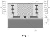
- FIG. 1 is a schematic cross-sectional structural view of an electro-optic modulator provided in Embodiment One of the present application.
- FIG. 2 to FIG. 7 are schematic cross-sectional structural views of structures obtained in each step of a method for preparing an electro-optic modulator provided in Embodiment One of the present application.
- FIG. 8 is a schematic cross-sectional structural view of the electro-optic modulator provided in Embodiment Two of the present application.
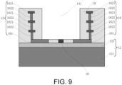
- FIG. 9 is a schematic cross-sectional structural view of a structure obtained after an opening is obtained in the method for preparing the electro-optic modulator provided in Embodiment Two of the present application.
- 10 waveguide
- 11 organic electro-optic material layer
- 12 substrate
- 121 base
- 122 second dielectric layer
- 13 silicon layer
- 14 first dielectric layer
- 141 opening
- 15 first electrode
- 16 second electrode
- 161 bottom electrode
- 1621 metal layer
- 1622 interconnecting plug
- first, second, third, “fourth”, etc. used in the present application may be used in the text to describe various elements, but these elements are not limited by these terms. These terms are only used to distinguish one element from another element.
- a first control device may be referred to as a second control device, and similarly, a second control device may be referred to as a first control device.
- the first control device and the second control device are both control devices, but they are not the same control device.
- connection in the following embodiments should be understood as “electrical connection”, “communication connection”, etc. if the connected circuits, modules, units, etc. have the transmission of electrical signals or data between each other.
- the electro-optic modulator includes: a substrate 12; a first dielectric layer 14 located on the substrate 12, an opening 141 being formed in the first dielectric layer 14, and the opening 141 exposing a portion of the substrate 12; a waveguide 10 located on the substrate 12 and located at the bottom of the opening 141; a first electrode 15 located in the first dielectric layer 14, located on one side of the waveguide 10, and spaced apart from the waveguide 10; a second electrode 16 located in the first dielectric layer 14, located on one side of the waveguide 10 distant from the first electrode 15, and spaced apart from the waveguide 10; and an organic electro-optic material layer 11 at least located in the opening 14 and at least covering the waveguide 10.
- the organic electro-optic material layer 11 covers the waveguide 10 in FIG. 1 .
- the waveguide 10 in the present application may be any non-slot waveguide. Since the waveguide 10 is a non-slot waveguide different from the current slot waveguide, the manufacturing process requirements are lower and the optical loss is lower.
- the organic electro-optic material layer is covered on the waveguide, so that a light field can be leaked into the organic electro-optic material to the maximum extent, thereby effectively reducing optical loss and having high electro-optic modulation efficiency.
- a working mode of the waveguide 10 is a TM mode, and herein, a width of the waveguide 10 may be set according to actual needs and may not be limited herein.
- a height of the waveguide 10 may be 150nm to 300nm, and specifically, the height of the waveguide 10 may be 150nm, 200nm, 250nm, or 300nm, etc.
- the working mode of the waveguide 10 is a TE mode, and herein, the height of the waveguide 10 may be set according to actual needs and may not be limited herein.
- the width of the waveguide 10 may be 300nm to 1000nm, and specifically, the width of the waveguide 10 may be 300nm, 400nm, 500nm, 600nm, 700nm, 800nm, 900nm, or 1000nm, etc.
- the working mode of the waveguide 10 is the TE mode, by limiting the width of the waveguide 10 within the above range, the light field can be leaked into the organic electro-optic material to the maximum extent, thereby effectively reducing optical loss and having high electro-optic modulation efficiency.
- the height of the waveguide 10 may be 150nm to 300nm, and the width of the waveguide 10 may be 300nm to 1000nm.
- the height of the waveguide 10 may be 150nm, 200nm, 250nm, or 300nm, etc.
- the width of the waveguide 10 may be 300nm, 400nm, 500nm, 600nm, 700nm, 800nm, 900nm, or 1000nm, etc.
- the working mode of the waveguide 10 is the TE mode or the TM mode
- the light field can be leaked into the organic electro-optic material to the maximum extent, thereby effectively reducing optical loss and having high electro-optic modulation efficiency.
- the substrate 12 may include a base 121 and a second dielectric layer 122 located on the base 121.
- both the first dielectric layer 14 and the waveguide 10 are located on the second dielectric layer 122.
- the base 121 may be but not limited to a silicon base.
- the second dielectric layer 122 may be but not limited to an oxide layer, such as a silicon oxide layer.
- a thickness of the base 121 may be greater than a thickness of the second dielectric layer 122.
- each of the first electrode 15 and the second electrode 16 may include: a bottom electrode 161 extending from the first dielectric layer 14 to the bottom of the opening 141, where a gap is provided between the bottom electrode 161 and the waveguide 10; a metal stack structure located in the first dielectric layer 14 and located on the bottom electrode 161.
- the metal stack structure includes a plurality of metal layers 1621 arranged at intervals and a plurality of interconnecting plugs 1622. The connection between the metal layer 1621 located on a top layer and the bottom electrode 161 and the connection between adjacent metal layers 1621 are made through the interconnecting plugs 1622, as shown in FIG. 1 .
- the bottom electrode 161 extends from the inside of the first dielectric layer 14 to the bottom of the opening 141.
- the gap between the bottom electrode 161 and the waveguide 10 may be adjusted to the required optimal range, thereby ensuring better electro-optic modulation efficiency with lower optical loss.
- the gap between the bottom electrode 161 and the waveguide 10 may be set according to actual needs.
- the gap between the bottom electrode 161 and the waveguide 10 may be but not limited to 500nm to 5000nm and to be specific, the gap between the bottom electrode 161 and the waveguide 10 may be 500nm, 1000nm, 2000nm, 3000nm, 4000nm, or 5000nm, etc.
- the bottom electrode 161 may be a doped silicon electrode.
- the electric field generated by the doped silicon electrode may achieve electro-optic modulation.
- the gap between the bottom electrode 161 and the waveguide 10 cannot be excessively far or excessively close. If the gap between the bottom electrode 161 and the waveguide 10 is excessively close (e.g., less than 500nm), the bottom electrode 161 may absorb the light field, resulting in higher optical loss. However, if the gap between the bottom electrode 161 and the waveguide 10 is excessively far (e.g., greater than 5000 nm), the electro-optic modulation effect of the electric field generated by the bottom electrode 161 may be relatively poor. By limiting the gap between the bottom electrode 161 and the waveguide 10 to 500nm to 5000nm, better electro-optic modulation efficiency may be achieved while ensuring lower optical loss.
- the waveguide 10 may be a silicon waveguide.
- the base 121, the second dielectric layer 122, the waveguide 10, and the bottom electrode 161 may be obtained based on a same silicon-on-insulator (SOI) substrate.
- the base 121 may be a back substrate of the SOI substrate
- the second dielectric layer 122 may be a buried oxide layer of the SOI substrate
- the waveguide 10 and the bottom electrode 161 may be obtained by patterning top silicon of the SOI substrate.
- the waveguide 10 is obtained by directly etching the top silicon of the SOI substrate
- the bottom electrode 161 is obtained by etching the top silicon of the SOI substrate and then performing ion implantation and doping.
- the bottom electrode 161 may specifically be a heavily doped silicon electrode.
- the first dielectric layer 14 is not provided between the bottom electrode 161 and the waveguide 10.
- the organic electro-optic material layer 11 fills the gap. That is, the organic electro-optic material layer 11 is filled between the bottom electrode layer 161 and the waveguide 10 herein, and the organic electro-optic material layer 11 fills the opening 141 and extends to fill the gap between the bottom electrode layer 161 and the waveguide 10 herein.
- the metal stack structure in the first electrode 15 and the metal stack structure in the second electrode 16 are located on opposite sides of the organic electro-optic material layer 11.
- the interconnecting plugs 1622 may be metal plugs.
- the interconnecting plugs 1622 may include but not limited to aluminum plugs, copper plugs, nickel plugs, titanium plugs, etc.
- the metal layers 1621 may include copper layers, nickel layers, aluminum layers, titanium layers, etc.
- an upper surface of the first dielectric layer 14 may be higher than an upper surface of the metal stack structure, and the first dielectric layer 14 may cover and protect the metal stack structure.
- the first dielectric layer 14 may include but not limited to an oxide layer.
- the first dielectric layer 14 may include but not limited to a silicon oxide layer.
- the organic electro-optic material layer 11 may be but not limited to a polyphenylene vinylene layer, a polyacetylene layer, a polyparaphenylene layer, a polythiophene layer, a polythiophene derivative layer, or a polyalkyl fluorene layer, etc.
- the present application further provides a method for preparing an electro-optic modulator, and the electro-optic modulator is used to prepare the electro-optic modulator in the above embodiment.
- the method for preparing the electro-optic modulator includes the following steps.
- a waveguide and a bottom electrode are formed on the substrate, and the bottom electrode is located on two opposite sides of the waveguide and is spaced apart from the waveguide.
- a first dielectric layer and a metal stack structure are formed, and the first dielectric layer covers the waveguide and the bottom electrode.
- the metal stack structure is located in the first dielectric layer and located on the bottom electrode.
- the metal stack structure includes a plurality of metal layers arranged at intervals and a plurality of interconnecting plugs. The connection between the metal layer located on a top layer and the bottom electrode and the connection between adjacent metal layers are made through the interconnecting plugs.
- an opening is formed in the first dielectric layer, and the opening exposes the waveguide and a portion of the substrate.
- an organic electro-optic material layer is formed in the opening, and the organic electro-optic material layer covers the waveguide 10 and a portion of the bottom electrode 161.
- the substrate 12 may include a base 121 and a second dielectric layer 122, and the second dielectric layer 122 is located on the base 121.
- the substrate 12 may be a silicon on insulator (SOI) substrate.
- the base 121 can be a back substrate of the SOI substrate
- the second dielectric layer 122 may be a buried oxide layer of the SOI substrate
- a top layer of silicon is formed on the second dielectric layer 122 as a silicon layer 13.
- step S20 as shown in FIGS. 3 to 4 , the formation of the waveguide 10 and the bottom electrode 161 on the substrate 12 may include the following steps:
- the silicon layer 13 is patterned to obtain a patterned silicon layer, as shown in FIG. 3 .
- a photolithography and etching process may be used to pattern the silicon layer 13, and the patterned silicon layer includes the waveguide 10 and defines a position and a shape of the bottom electrode 161.
- the bottom electrode 161 is a doped silicon electrode, and a doping concentration of the bottom electrode 161 may be set according to actual needs.
- the bottom electrode 161 may include but not limited to a heavily doped silicon electrode.
- step S30 the formation of the first dielectric layer 14 and the metal stack structure may include the following steps:
- a bottom dielectric layer is formed, and the bottom dielectric layer covers the waveguide 10 and the bottom electrode 161.
- an interconnecting via is formed in the bottom dielectric layer, the interconnecting via exposes the bottom electrode 161, and the interconnecting plug 1622 located on a bottom layer is formed in the interconnecting via.
- the metal layer 1621 located on the bottom layer is formed on an upper surface of the bottom dielectric layer, and the metal layer 1621 located on the bottom layer is in contact with the interconnecting plug 1622 located on the bottom layer.
- an interlayer dielectric layer is formed on the upper surface of the formed dielectric layer, and the interlayer dielectric layer covers the formed metal layer 1621.
- an interconnecting via is formed in the interlayer dielectric layer, the interconnecting via exposes the metal layer 1621 covered by the interlayer dielectric layer, and the interconnecting plug 1622 between layers is formed in the interconnecting via.
- the metal layer 1621 between layers is formed on an upper surface of the interlayer dielectric layer, and the metal layer 1621 between layers is in contact with the interconnecting plug 1622 between layers.
- the metal layer 1621 located on the top layer is formed on the upper surface of the interlayer dielectric layer that is formed last.
- a top dielectric layer is formed, and the top dielectric layer covers the metal layer 1621 located on the top layer.
- the dielectric layers in steps S301 to S309 together constitute the first dielectric layer 14, that is, the bottom dielectric layer, the interlayer dielectric layer, and the top dielectric layer together constitute the first dielectric layer 14.
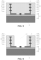
- the structure obtained in step S30 is shown in FIG. 5 .
- step S40 a photolithography process may be used to form the opening 141, and the structure obtained in step S40 is shown in FIG. 6 .
- the opening 141 in this embodiment completely exposes an upper surface and side surfaces of the waveguide 10, the opening 141 extends between the waveguide 10 and the bottom electrode 161, and the bottom of the opening 141 is flush with the bottom of the waveguide 10.
- the organic electro-optic material layer 11 may be formed using but not limited to a physical vapor deposition process, a chemical vapor deposition process, or an atomic layer deposition process.
- the organic electro-optic material layer 11 fills the opening 141 and extends to fill the gap between the bottom electrode layer 161 and the waveguide 10, and the structure obtained in step S50 is shown in FIG. 7 .
- the present application further provides an electro-optic modulator.
- the structure of the electro-optic modulator in this embodiment is substantially the same as that of the electro-optic modulator in Embodiment One, and the differences therebetween are as follows:
- the waveguide 10 is located at the bottom of the opening, the first dielectric layer 14 is not provided between the bottom electrode 161 and the waveguide 10, and herein, the organic electro-optic material layer 11 fills the gap.
- the organic electro-optic material layer 11 is filled between the bottom electrode layer 161 and the waveguide 10 herein, and the organic electro-optic material layer 11 fills the opening 141 and extends to fill the gap between the bottom electrode layer 161 and the waveguide 10 herein.
- the waveguide 10 is located below the opening 141, and the first dielectric layer 14 also fills the gap, that is, the first dielectric layer 14 is provided between the bottom electrode 161 and the waveguide 10 herein.
- the organic electro-optic material layer 11 is completely located above the waveguide 10 and covers the upper surface of the waveguide 10.
- the upper surface of bottom electrode 161 may be flush with the upper surface of waveguide 10.
- the upper surface of the first dielectric layer 14 located between the bottom electrode 161 and the waveguide 10 is flush with the upper surface of the bottom electrode 161 and the upper surface of the waveguide 10.
- the present application further provides a method for preparing an electro-optic modulator.
- the method for preparing the electro-optic modulator in this embodiment is substantially the same as the method for preparing the electro-optic modulator in Embodiment One, and the differences therebetween are as follows:
- step S40 and step S50 the opening formed in step S40 in the Embodiment One completely exposes the upper surface and the side surfaces of the waveguide 10, the opening 141 extends between the waveguide 10 and the bottom electrode 161, and the bottom of the opening 141 is flush with the bottom of the waveguide 10.
- the organic electro-optic material layer 11 formed in step S50 fills the opening 141 and extends to fill the gap between the bottom electrode layer 161 and the waveguide 10.
- the opening in the present application only exposes the upper surface of the waveguide 10, the opening 141 does not extend between the waveguide 10 and the bottom electrode 161, and the bottom of the opening 141 is flush with the top of the waveguide 10, as shown in FIG. 9 .
- the organic electro-optic material layer 11 in step S50 is completely located above the waveguide 10 and covers the upper surface of the waveguide 10.
Landscapes
- Physics & Mathematics (AREA)
- Nonlinear Science (AREA)
- General Physics & Mathematics (AREA)
- Optics & Photonics (AREA)
- Chemical & Material Sciences (AREA)
- Engineering & Computer Science (AREA)
- Ceramic Engineering (AREA)
- Crystallography & Structural Chemistry (AREA)
- Optical Modulation, Optical Deflection, Nonlinear Optics, Optical Demodulation, Optical Logic Elements (AREA)
Applications Claiming Priority (2)
| Application Number | Priority Date | Filing Date | Title |
|---|---|---|---|
| CN202122193530.0U CN215813606U (zh) | 2021-09-10 | 2021-09-10 | 电光调制器 |
| PCT/CN2022/085508 WO2023035606A1 (fr) | 2021-09-10 | 2022-04-07 | Modulateur électro-optique |
Publications (2)
| Publication Number | Publication Date |
|---|---|
| EP4400902A1 true EP4400902A1 (fr) | 2024-07-17 |
| EP4400902A4 EP4400902A4 (fr) | 2025-09-10 |
Family
ID=80158748
Family Applications (1)
| Application Number | Title | Priority Date | Filing Date |
|---|---|---|---|
| EP22866084.1A Pending EP4400902A4 (fr) | 2021-09-10 | 2022-04-07 | Modulateur électro-optique |
Country Status (4)
| Country | Link |
|---|---|
| US (1) | US20240210742A1 (fr) |
| EP (1) | EP4400902A4 (fr) |
| CN (1) | CN215813606U (fr) |
| WO (1) | WO2023035606A1 (fr) |
Families Citing this family (4)
| Publication number | Priority date | Publication date | Assignee | Title |
|---|---|---|---|---|
| CN215813606U (zh) * | 2021-09-10 | 2022-02-11 | 苏州湃矽科技有限公司 | 电光调制器 |
| CN117687230A (zh) * | 2022-09-05 | 2024-03-12 | 华为技术有限公司 | 一种移相器、调制器和相关设备 |
| US20240393654A1 (en) * | 2023-05-28 | 2024-11-28 | Quantum Transistors Technology Ltd. | Silicon photonics phase modulators and their applications |
| CN220829639U (zh) * | 2023-09-18 | 2024-04-23 | 苏州旭创科技有限公司 | 光调制器 |
Family Cites Families (7)
| Publication number | Priority date | Publication date | Assignee | Title |
|---|---|---|---|---|
| US7218799B2 (en) * | 2005-03-29 | 2007-05-15 | Analog Devices, Inc. | External optical modulator |
| WO2015171125A1 (fr) * | 2014-05-07 | 2015-11-12 | Hewlett-Packard Development Company, L.P. | Modulateurs optiques à gaine polymère |
| CN205942163U (zh) * | 2016-07-11 | 2017-02-08 | 派尼尔科技(天津)有限公司 | 一种采用脊形波导的马赫曾德光调制器晶片结构 |
| CN112415786A (zh) * | 2019-08-22 | 2021-02-26 | 苏州旭创科技有限公司 | 一种硅基电光调制器 |
| CN112485931B (zh) * | 2019-09-12 | 2023-04-21 | 苏州旭创科技有限公司 | 一种电光调制器 |
| CN111175999B (zh) * | 2020-02-24 | 2021-05-04 | 上海交通大学 | 基于铌酸锂-硅晶圆的高速低电压电光调制器 |
| CN215813606U (zh) * | 2021-09-10 | 2022-02-11 | 苏州湃矽科技有限公司 | 电光调制器 |
-
2021
- 2021-09-10 CN CN202122193530.0U patent/CN215813606U/zh active Active
-
2022
- 2022-04-07 EP EP22866084.1A patent/EP4400902A4/fr active Pending
- 2022-04-07 WO PCT/CN2022/085508 patent/WO2023035606A1/fr not_active Ceased
-
2024
- 2024-03-07 US US18/599,130 patent/US20240210742A1/en active Pending
Also Published As
| Publication number | Publication date |
|---|---|
| CN215813606U (zh) | 2022-02-11 |
| US20240210742A1 (en) | 2024-06-27 |
| WO2023035606A1 (fr) | 2023-03-16 |
| EP4400902A4 (fr) | 2025-09-10 |
Similar Documents
| Publication | Publication Date | Title |
|---|---|---|
| EP4400902A1 (fr) | Modulateur électro-optique | |
| US10969547B2 (en) | Optoelectronic device and method of manufacturing thereof | |
| US20200313021A1 (en) | Photodetector | |
| CN102763264B (zh) | 一种移相器和耦合器及其制造方法 | |
| CN111051969B (zh) | 相位调制器及其制作方法、硅基电光调制器 | |
| KR20110112126A (ko) | 실리콘 기반 광변조기 | |
| US20240210743A1 (en) | Electro-optic modulator and preparation method therefor | |
| US20230003943A1 (en) | Manufacture of semiconductor device with optical transmission channel between optical coupler and outside of the semiconductor device | |
| JP6386039B2 (ja) | 欠陥の少ないエピタキシャルフォトニックデバイスを提供する方法およびその結果生じる構造 | |
| KR20160087960A (ko) | 전계흡수 광변조 소자 및 그 제조 방법 | |
| EP3462232B1 (fr) | Modulateur d'électro-absorption | |
| CN111562687A (zh) | 制作半导体器件的方法、半导体器件和半导体集成电路 | |
| US9206526B2 (en) | Method for the formation of nano-scale on-chip optical waveguide structures | |
| CN107037534B (zh) | 可集成光电器件及其制作方法、多个光电器件的集成方法 | |
| KR101278611B1 (ko) | 반도체 장치 및 그 형성 방법 | |
| CN111580289A (zh) | 制作半导体器件的方法、半导体器件和半导体集成电路 | |
| CN105185787B (zh) | 制作阵列基板的方法、阵列基板以及液晶显示面板 | |
| CN120255077A (zh) | 光子集成电路芯片及光子集成电路芯片的制造方法 | |
| CN120522915A (zh) | 集成光学结构及其制备方法 | |
| KR100320437B1 (ko) | 반도체 소자의 제조방법 | |
| CN118938519A (zh) | 半导体结构及其形成方法 | |
| CN117393620A (zh) | 光电探测器及其形成方法 | |
| CN120233486A (zh) | 光子集成电路芯片的制造方法及光子集成电路芯片 | |
| CN120730834A (zh) | 阵列基板及其制备方法、显示面板 | |
| WO2021048018A1 (fr) | Dispositif optoélectronique et procédé de fabrication d'un dispositif optoélectronique |
Legal Events
| Date | Code | Title | Description |
|---|---|---|---|
| STAA | Information on the status of an ep patent application or granted ep patent |
Free format text: STATUS: THE INTERNATIONAL PUBLICATION HAS BEEN MADE |
|
| PUAI | Public reference made under article 153(3) epc to a published international application that has entered the european phase |
Free format text: ORIGINAL CODE: 0009012 |
|
| STAA | Information on the status of an ep patent application or granted ep patent |
Free format text: STATUS: REQUEST FOR EXAMINATION WAS MADE |
|
| 17P | Request for examination filed |
Effective date: 20240327 |
|
| AK | Designated contracting states |
Kind code of ref document: A1 Designated state(s): AL AT BE BG CH CY CZ DE DK EE ES FI FR GB GR HR HU IE IS IT LI LT LU LV MC MK MT NL NO PL PT RO RS SE SI SK SM TR |
|
| DAV | Request for validation of the european patent (deleted) | ||
| DAX | Request for extension of the european patent (deleted) | ||
| A4 | Supplementary search report drawn up and despatched |
Effective date: 20250807 |
|
| RIC1 | Information provided on ipc code assigned before grant |
Ipc: G02F 1/065 20060101AFI20250801BHEP Ipc: G02F 1/061 20060101ALI20250801BHEP Ipc: G02F 1/025 20060101ALI20250801BHEP |