EP4400876A2 - Induced transmission filter - Google Patents
Induced transmission filter Download PDFInfo
- Publication number
- EP4400876A2 EP4400876A2 EP24177928.9A EP24177928A EP4400876A2 EP 4400876 A2 EP4400876 A2 EP 4400876A2 EP 24177928 A EP24177928 A EP 24177928A EP 4400876 A2 EP4400876 A2 EP 4400876A2
- Authority
- EP
- European Patent Office
- Prior art keywords
- filter
- approximately
- degrees
- dielectric
- optical
- Prior art date
- Legal status (The legal status is an assumption and is not a legal conclusion. Google has not performed a legal analysis and makes no representation as to the accuracy of the status listed.)
- Pending
Links
- 230000005540 biological transmission Effects 0.000 title description 14
- 230000003287 optical effect Effects 0.000 claims abstract description 140
- 229910052751 metal Inorganic materials 0.000 claims abstract description 36
- 239000002184 metal Substances 0.000 claims abstract description 36
- 230000003595 spectral effect Effects 0.000 claims abstract description 29
- 238000001914 filtration Methods 0.000 claims abstract description 4
- 238000000034 method Methods 0.000 claims abstract 9
- 239000000463 material Substances 0.000 claims description 27
- 229910052709 silver Inorganic materials 0.000 claims description 18
- 239000004332 silver Substances 0.000 claims description 18
- 238000001429 visible spectrum Methods 0.000 claims description 4
- VYPSYNLAJGMNEJ-UHFFFAOYSA-N Silicium dioxide Chemical compound O=[Si]=O VYPSYNLAJGMNEJ-UHFFFAOYSA-N 0.000 description 54
- OBOYOXRQUWVUFU-UHFFFAOYSA-N [O-2].[Ti+4].[Nb+5] Chemical compound [O-2].[Ti+4].[Nb+5] OBOYOXRQUWVUFU-UHFFFAOYSA-N 0.000 description 36
- XLOMVQKBTHCTTD-UHFFFAOYSA-N Zinc monoxide Chemical compound [Zn]=O XLOMVQKBTHCTTD-UHFFFAOYSA-N 0.000 description 29
- 239000003989 dielectric material Substances 0.000 description 29
- 239000000758 substrate Substances 0.000 description 28
- 239000000377 silicon dioxide Substances 0.000 description 27
- 235000012239 silicon dioxide Nutrition 0.000 description 22
- BQCADISMDOOEFD-UHFFFAOYSA-N Silver Chemical compound [Ag] BQCADISMDOOEFD-UHFFFAOYSA-N 0.000 description 16
- 229910052581 Si3N4 Inorganic materials 0.000 description 15
- HQVNEWCFYHHQES-UHFFFAOYSA-N silicon nitride Chemical compound N12[Si]34N5[Si]62N3[Si]51N64 HQVNEWCFYHHQES-UHFFFAOYSA-N 0.000 description 15
- 238000010586 diagram Methods 0.000 description 14
- 239000011787 zinc oxide Substances 0.000 description 13
- 230000000903 blocking effect Effects 0.000 description 6
- 239000011521 glass Substances 0.000 description 5
- 239000007769 metal material Substances 0.000 description 4
- ZKATWMILCYLAPD-UHFFFAOYSA-N niobium pentoxide Inorganic materials O=[Nb](=O)O[Nb](=O)=O ZKATWMILCYLAPD-UHFFFAOYSA-N 0.000 description 4
- URLJKFSTXLNXLG-UHFFFAOYSA-N niobium(5+);oxygen(2-) Chemical compound [O-2].[O-2].[O-2].[O-2].[O-2].[Nb+5].[Nb+5] URLJKFSTXLNXLG-UHFFFAOYSA-N 0.000 description 4
- TWNQGVIAIRXVLR-UHFFFAOYSA-N oxo(oxoalumanyloxy)alumane Chemical compound O=[Al]O[Al]=O TWNQGVIAIRXVLR-UHFFFAOYSA-N 0.000 description 4
- SIWVEOZUMHYXCS-UHFFFAOYSA-N oxo(oxoyttriooxy)yttrium Chemical compound O=[Y]O[Y]=O SIWVEOZUMHYXCS-UHFFFAOYSA-N 0.000 description 4
- BPUBBGLMJRNUCC-UHFFFAOYSA-N oxygen(2-);tantalum(5+) Chemical compound [O-2].[O-2].[O-2].[O-2].[O-2].[Ta+5].[Ta+5] BPUBBGLMJRNUCC-UHFFFAOYSA-N 0.000 description 4
- RVTZCBVAJQQJTK-UHFFFAOYSA-N oxygen(2-);zirconium(4+) Chemical compound [O-2].[O-2].[Zr+4] RVTZCBVAJQQJTK-UHFFFAOYSA-N 0.000 description 4
- PBCFLUZVCVVTBY-UHFFFAOYSA-N tantalum pentoxide Inorganic materials O=[Ta](=O)O[Ta](=O)=O PBCFLUZVCVVTBY-UHFFFAOYSA-N 0.000 description 4
- 229910001928 zirconium oxide Inorganic materials 0.000 description 4
- 239000004593 Epoxy Substances 0.000 description 3
- 101000863856 Homo sapiens Shiftless antiviral inhibitor of ribosomal frameshifting protein Proteins 0.000 description 3
- 238000005516 engineering process Methods 0.000 description 3
- PFNQVRZLDWYSCW-UHFFFAOYSA-N (fluoren-9-ylideneamino) n-naphthalen-1-ylcarbamate Chemical compound C12=CC=CC=C2C2=CC=CC=C2C1=NOC(=O)NC1=CC=CC2=CC=CC=C12 PFNQVRZLDWYSCW-UHFFFAOYSA-N 0.000 description 2
- KRHYYFGTRYWZRS-UHFFFAOYSA-M Fluoride anion Chemical compound [F-] KRHYYFGTRYWZRS-UHFFFAOYSA-M 0.000 description 2
- UCKMPCXJQFINFW-UHFFFAOYSA-N Sulphide Chemical compound [S-2] UCKMPCXJQFINFW-UHFFFAOYSA-N 0.000 description 2
- GWEVSGVZZGPLCZ-UHFFFAOYSA-N Titan oxide Chemical compound O=[Ti]=O GWEVSGVZZGPLCZ-UHFFFAOYSA-N 0.000 description 2
- 239000005083 Zinc sulfide Substances 0.000 description 2
- 238000004891 communication Methods 0.000 description 2
- 230000000295 complement effect Effects 0.000 description 2
- 230000001419 dependent effect Effects 0.000 description 2
- 230000008021 deposition Effects 0.000 description 2
- CJNBYAVZURUTKZ-UHFFFAOYSA-N hafnium(iv) oxide Chemical compound O=[Hf]=O CJNBYAVZURUTKZ-UHFFFAOYSA-N 0.000 description 2
- ORUIBWPALBXDOA-UHFFFAOYSA-L magnesium fluoride Chemical compound [F-].[F-].[Mg+2] ORUIBWPALBXDOA-UHFFFAOYSA-L 0.000 description 2
- 229910001635 magnesium fluoride Inorganic materials 0.000 description 2
- 238000005259 measurement Methods 0.000 description 2
- 150000004767 nitrides Chemical class 0.000 description 2
- 150000003346 selenoethers Chemical class 0.000 description 2
- 239000004065 semiconductor Substances 0.000 description 2
- 229910052984 zinc sulfide Inorganic materials 0.000 description 2
- XUIMIQQOPSSXEZ-UHFFFAOYSA-N Silicon Chemical compound [Si] XUIMIQQOPSSXEZ-UHFFFAOYSA-N 0.000 description 1
- 150000002290 germanium Chemical class 0.000 description 1
- 229910052732 germanium Inorganic materials 0.000 description 1
- GNPVGFCGXDBREM-UHFFFAOYSA-N germanium atom Chemical compound [Ge] GNPVGFCGXDBREM-UHFFFAOYSA-N 0.000 description 1
- 239000003292 glue Substances 0.000 description 1
- 238000005286 illumination Methods 0.000 description 1
- 238000003384 imaging method Methods 0.000 description 1
- 230000000977 initiatory effect Effects 0.000 description 1
- 238000012986 modification Methods 0.000 description 1
- 230000004048 modification Effects 0.000 description 1
- 239000002861 polymer material Substances 0.000 description 1
- 229920000307 polymer substrate Polymers 0.000 description 1
- 150000003376 silicon Chemical class 0.000 description 1
- 229910052710 silicon Inorganic materials 0.000 description 1
- 239000010703 silicon Substances 0.000 description 1
- DRDVZXDWVBGGMH-UHFFFAOYSA-N zinc;sulfide Chemical compound [S-2].[Zn+2] DRDVZXDWVBGGMH-UHFFFAOYSA-N 0.000 description 1
Images


Classifications
-
- H—ELECTRICITY
- H01—ELECTRIC ELEMENTS
- H01L—SEMICONDUCTOR DEVICES NOT COVERED BY CLASS H10
- H01L27/00—Devices consisting of a plurality of semiconductor or other solid-state components formed in or on a common substrate
- H01L27/14—Devices consisting of a plurality of semiconductor or other solid-state components formed in or on a common substrate including semiconductor components sensitive to infrared radiation, light, electromagnetic radiation of shorter wavelength or corpuscular radiation and specially adapted either for the conversion of the energy of such radiation into electrical energy or for the control of electrical energy by such radiation
- H01L27/144—Devices controlled by radiation
- H01L27/146—Imager structures
- H01L27/14601—Structural or functional details thereof
- H01L27/1462—Coatings
- H01L27/14621—Colour filter arrangements
-
- C—CHEMISTRY; METALLURGY
- C23—COATING METALLIC MATERIAL; COATING MATERIAL WITH METALLIC MATERIAL; CHEMICAL SURFACE TREATMENT; DIFFUSION TREATMENT OF METALLIC MATERIAL; COATING BY VACUUM EVAPORATION, BY SPUTTERING, BY ION IMPLANTATION OR BY CHEMICAL VAPOUR DEPOSITION, IN GENERAL; INHIBITING CORROSION OF METALLIC MATERIAL OR INCRUSTATION IN GENERAL
- C23C—COATING METALLIC MATERIAL; COATING MATERIAL WITH METALLIC MATERIAL; SURFACE TREATMENT OF METALLIC MATERIAL BY DIFFUSION INTO THE SURFACE, BY CHEMICAL CONVERSION OR SUBSTITUTION; COATING BY VACUUM EVAPORATION, BY SPUTTERING, BY ION IMPLANTATION OR BY CHEMICAL VAPOUR DEPOSITION, IN GENERAL
- C23C28/00—Coating for obtaining at least two superposed coatings either by methods not provided for in a single one of groups C23C2/00 - C23C26/00 or by combinations of methods provided for in subclasses C23C and C25C or C25D
-
- G—PHYSICS
- G02—OPTICS
- G02B—OPTICAL ELEMENTS, SYSTEMS OR APPARATUS
- G02B5/00—Optical elements other than lenses
- G02B5/20—Filters
-
- G—PHYSICS
- G02—OPTICS
- G02B—OPTICAL ELEMENTS, SYSTEMS OR APPARATUS
- G02B5/00—Optical elements other than lenses
- G02B5/20—Filters
- G02B5/201—Filters in the form of arrays
-
- G—PHYSICS
- G02—OPTICS
- G02B—OPTICAL ELEMENTS, SYSTEMS OR APPARATUS
- G02B5/00—Optical elements other than lenses
- G02B5/20—Filters
- G02B5/26—Reflecting filters
-
- G—PHYSICS
- G02—OPTICS
- G02B—OPTICAL ELEMENTS, SYSTEMS OR APPARATUS
- G02B5/00—Optical elements other than lenses
- G02B5/20—Filters
- G02B5/28—Interference filters
-
- G—PHYSICS
- G02—OPTICS
- G02B—OPTICAL ELEMENTS, SYSTEMS OR APPARATUS
- G02B5/00—Optical elements other than lenses
- G02B5/20—Filters
- G02B5/28—Interference filters
- G02B5/285—Interference filters comprising deposited thin solid films
-
- H—ELECTRICITY
- H01—ELECTRIC ELEMENTS
- H01B—CABLES; CONDUCTORS; INSULATORS; SELECTION OF MATERIALS FOR THEIR CONDUCTIVE, INSULATING OR DIELECTRIC PROPERTIES
- H01B3/00—Insulators or insulating bodies characterised by the insulating materials; Selection of materials for their insulating or dielectric properties
- H01B3/02—Insulators or insulating bodies characterised by the insulating materials; Selection of materials for their insulating or dielectric properties mainly consisting of inorganic substances
- H01B3/025—Other inorganic material
-
- H—ELECTRICITY
- H01—ELECTRIC ELEMENTS
- H01B—CABLES; CONDUCTORS; INSULATORS; SELECTION OF MATERIALS FOR THEIR CONDUCTIVE, INSULATING OR DIELECTRIC PROPERTIES
- H01B3/00—Insulators or insulating bodies characterised by the insulating materials; Selection of materials for their insulating or dielectric properties
- H01B3/02—Insulators or insulating bodies characterised by the insulating materials; Selection of materials for their insulating or dielectric properties mainly consisting of inorganic substances
- H01B3/10—Insulators or insulating bodies characterised by the insulating materials; Selection of materials for their insulating or dielectric properties mainly consisting of inorganic substances metallic oxides
-
- H—ELECTRICITY
- H01—ELECTRIC ELEMENTS
- H01L—SEMICONDUCTOR DEVICES NOT COVERED BY CLASS H10
- H01L27/00—Devices consisting of a plurality of semiconductor or other solid-state components formed in or on a common substrate
- H01L27/14—Devices consisting of a plurality of semiconductor or other solid-state components formed in or on a common substrate including semiconductor components sensitive to infrared radiation, light, electromagnetic radiation of shorter wavelength or corpuscular radiation and specially adapted either for the conversion of the energy of such radiation into electrical energy or for the control of electrical energy by such radiation
- H01L27/144—Devices controlled by radiation
- H01L27/146—Imager structures
- H01L27/148—Charge coupled imagers
- H01L27/14806—Structural or functional details thereof
-
- G—PHYSICS
- G02—OPTICS
- G02B—OPTICAL ELEMENTS, SYSTEMS OR APPARATUS
- G02B5/00—Optical elements other than lenses
- G02B5/20—Filters
- G02B5/28—Interference filters
- G02B5/281—Interference filters designed for the infrared light
- G02B5/282—Interference filters designed for the infrared light reflecting for infrared and transparent for visible light, e.g. heat reflectors, laser protection
-
- Y—GENERAL TAGGING OF NEW TECHNOLOGICAL DEVELOPMENTS; GENERAL TAGGING OF CROSS-SECTIONAL TECHNOLOGIES SPANNING OVER SEVERAL SECTIONS OF THE IPC; TECHNICAL SUBJECTS COVERED BY FORMER USPC CROSS-REFERENCE ART COLLECTIONS [XRACs] AND DIGESTS
- Y02—TECHNOLOGIES OR APPLICATIONS FOR MITIGATION OR ADAPTATION AGAINST CLIMATE CHANGE
- Y02E—REDUCTION OF GREENHOUSE GAS [GHG] EMISSIONS, RELATED TO ENERGY GENERATION, TRANSMISSION OR DISTRIBUTION
- Y02E10/00—Energy generation through renewable energy sources
- Y02E10/50—Photovoltaic [PV] energy
- Y02E10/52—PV systems with concentrators
Definitions
- An optical sensor device may be utilized to capture information.
- the optical sensor device may capture information relating to a set of electromagnetic frequencies.
- the optical sensor device may include a set of sensor elements (e.g., optical sensors, spectral sensors, and/or image sensors) that capture the information.
- an array of sensor elements may be utilized to capture information relating to multiple frequencies.
- an array of sensor elements may be utilized to capture information regarding a set of color bands of light, such as a first sensor element, of the sensor element array, capturing information regarding a red band of light; a second sensor element, of the sensor element array, capturing information regarding a green band of light; a third sensor element, of the sensor element array, capturing information regarding a blue band of light, or the like.
- a sensor element, of the sensor element array may be associated with a filter.
- the filter may include a passband associated with a first spectral range of light that is passed to the sensor element.
- the filter may be associated with blocking a second spectral range of light from being passed to the sensor element.
- a sensor element array may be associated with a filter including different color passbands, such as a red passband, a blue passband, a green passband, or the like (e.g., a red-green-blue (RGB) filter).
- RGB red-green-blue
- a sensor element array be associated with a near infrared (NIR) blocking filter, an infrared (IR) blocking filter, a long wave pass (LWP) filter, a short wave pass (SWP) filter, a photopic filter, a tristimulus filter, or the like.
- NIR near infrared
- IR infrared
- LWP long wave pass
- SWP short wave pass
- photopic filter a tristimulus filter
- an optical filter may include a first group of layers.
- the first group of layers may include alternating layers of a first dielectric material, of a group of dielectric materials, and a second dielectric material of the group of dielectric materials.
- the optical filter may include a second group of layers.
- the second group of layers may include alternating layers of a third dielectric material, of the group of dielectric materials, and a fourth dielectric material of the group of dielectric materials.
- the optical filter may include a third group of layers.
- the third group of layers may include alternating layers of a fifth dielectric material, of the group of dielectric materials, a sixth dielectric material, of the group of dielectric materials, and a metal material.
- the third group of layers may be disposed between the first group of layers and the second group of layers.
- the group of dielectric materials may consist of two materials.
- the group of dielectric materials may consist of three materials.
- the group of dielectric materials may include at least one of: niobium titanium oxide (NbTiO x ), silicon dioxide (SiO2), aluminum oxide (Al 2 O 3 ), titanium dioxide (TiO 2 ), niobium pentoxide (Nb 2 O 5 ), tantalum pentoxide (Ta 2 O 5 ), zirconium oxide (ZrO 2 ), yttrium oxide (Y 2 O 3 ), hafnium dioxide (HfO 2 ), or a combination thereof.
- the group of dielectric materials may include at least one of: a nitride material, a fluoride material, a sulfide material, a selenide material, or a combination thereof.
- the metal material may be a silver material.
- the optical filter may further comprise a glass substrate, the first group of layers being deposited onto the glass substrate, the third group of layers being deposited onto the first group of layers, the second group of layers being deposited onto the third group of layers.
- the optical filter may further comprise: a detector including a detector substrate, the first group of layers being deposited onto the detector substrate, the third group of layers being deposited onto the first group of layers, the second group of layers being deposited onto the third group of layers.
- the detector may be at least one of: a complementary metal-oxide-semiconductor (CMOS) detector, a charge-coupled device detector, a front illuminated detector, or a back illuminated detector.
- CMOS complementary metal-oxide-semiconductor
- the first group of layers and the second group of layers may not include a metal layer.
- At least one dielectric material, of the group of dielectric materials may be associated with a refractive index greater than approximately 2.0.
- At least one dielectric material, of the group of dielectric materials may be associated with a refractive index less than approximately 3.0.
- An angle shift of a cut-off wavelength may be less than approximately 30 nm at a range of angles of incidence from 0 degrees to 50 degrees.
- An average transmissivity in a passband of a spectral range of between approximately 420 nm and approximately 620 nm may be greater than approximately 70% at a range of angles of incidence from 0 degrees to 50 degrees.
- an induced transmission filter may include a first all-dielectric portion including a first set of dielectric layers.
- the induced transmission filter may include a second all-dielectric portion including a second set of dielectric layers.
- the induced transmission filter may include a metal/dielectric portion including a third set of dielectric layers and one or more metal layers. The metal/dielectric portion may be disposed between the first all-dielectric portion and the second all-dielectric portion.
- the first set of dielectric layers and the second set of dielectric layers may each include alternating layers of a first dielectric material with a first refractive index and a second dielectric material with a second refractive index, the first refractive index may be higher than the second refractive index.
- the first set of dielectric layers, the second set of dielectric layers, and the third set of dielectric layers may each include at least one material in common.
- the metal/dielectric portion may include a set of layers arranged in a layer group, the layer group may include a plurality of layers in an order of a first layer of a first dielectric material, a second layer of a second dielectric material, a third layer of a metal material, a fourth layer of the second dielectric material, and a fifth layer of the first dielectric material.
- a mixed metal/dielectric optical filter may include a substrate.
- the mixed metal/dielectric optical filter may include a first all-dielectric portion including alternating silicon dioxide layers and niobium titanium oxide layers.
- the mixed metal/dielectric optical filter may include a second all-dielectric portion including alternating silicon dioxide layers and niobium titanium oxide layers.
- the mixed metal/dielectric optical filter may include a metal/dielectric portion including one or more layer groups.
- a layer group, of the one or more layer groups may include a silver layer, two zinc oxide layers, and two niobium titanium oxide layers.
- the silver layer may be disposed between the two zinc oxide layers.
- the two zinc oxide layers may be disposed between the two niobium titanium oxide layers.
- the metal/dielectric portion may be disposed between the first all-dielectric portion and the second all-dielectric portion.
- the mixed metal/dielectric optical filter may comprise at least one of: a color filter, a bandpass filter, a near infrared blocker, long wave pass (LWP) filter, a short wave pass (SWP) filter, a photopic filter, or a tristimulus filter.
- a color filter a bandpass filter, a near infrared blocker, long wave pass (LWP) filter, a short wave pass (SWP) filter, a photopic filter, or a tristimulus filter.
- An optical sensor device may include a sensor element array of sensor elements to receive light initiating from an optical source, such as an optical transmitter, a light bulb, an ambient light source, or the like.
- the optical sensor device may utilize one or more sensor technologies, such as a complementary metal-oxide-semiconductor (CMOS) technology, a charge-coupled device (CCD) technology, or the like.
- CMOS complementary metal-oxide-semiconductor
- CCD charge-coupled device
- a sensor element e.g., an optical sensor
- a sensor element may be associated with a filter that filters light to the sensor element to enable the sensor element to obtain information regarding a particular spectral range of electromagnetic frequencies.
- the sensor element may be aligned with a red-green-blue (RGB) filter, a near infrared (NIR) blocking filter, an infrared (IR) blocking filter, a long wave pass (LWP) filter, a short wave pass (SWP) filter, a photopic filter, a tristimulus filter, or the like to cause a portion of light that is directed toward the sensor element to be filtered.
- RGB red-green-blue
- NIR near infrared
- LWP long wave pass
- SWP short wave pass
- a filter may include sets of dielectric layers to filter the portion of the light.
- a filter may include dielectric filter stacks of alternating high-index layers and low-index layers, such as alternating layers of niobium titanium oxide (NbTiO x ) and silicon dioxide (SiO 2 ).
- all-dielectric types of filters may be associated with a threshold angle shift at increasing angles of incidence.
- an all-dielectric filter may be associated with an angle shift of greater than approximately 10 nm at an angle of incidence of 20 degrees, greater than approximately 20 nm at an angle of incidence of 30 degrees, greater than approximately 40 nm at an angle of incidence of 40 degrees, greater than approximately 50 nm at an angle of incidence of 50 degrees, or the like.
- a low angle shift (LAS) filter with alternating layers of high-index dielectric, low-index dielectric, and metal may be selected to reduce an angle shift relative to an all-dielectric filter.
- a low angle shift filter may utilize layers of niobium titanium oxide, zinc oxide, and silver to reduce an angle shift relative to an all-dielectric filter.
- the low angle shift filter may be associated with a transmissivity in a passband of the low angle shift filter that does not satisfy a threshold.
- a low angle shift filter may be associated with a transmissivity of less than approximately 70% at a range of angles of incidence from 0 degrees to 50 degrees.
- an optical filter may include a first portion with a set of alternating high-index layers of niobium titanium oxide and low-index layers of silicon dioxide, a second portion with another set of alternating high-index layers of niobium titanium oxide and low-index layers of silicon dioxide, and a third portion, disposed between the first portion and the second portion, of alternating layers of high-index layers of niobium titanium oxide, low-index layers of zinc oxide, and metal layers of silver.
- the filter may filter light with less than a threshold angle shift and with greater than a threshold level of transmission.
- a mixed dielectric/metal filter may be associated with an angle shift of less than approximately 30 nm at angles of incidence from 0 degrees to 50 degrees, an angle shift of less than approximately 20 nm at angles of incidence from 0 degrees to 40 degrees, an angle shift of less than approximately 10 nm at angles of incidence from 0 degrees to 20 degrees, or the like.
- a mixed dielectric/metal filter may be associated with a transmissivity of greater than approximately 70% at angles of incidence from 0 degrees to 50 degrees, greater than approximately 75% at angles of incidence from 0 degrees to 50 degrees, or the like.
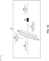
- Figs. 1A-1C are a diagrams of an overview of example implementations 100/100'/100" described herein.
- example implementation 100 includes a sensor system 110.
- Sensor system 110 may be a portion of an optical system, and may provide an electrical output corresponding to a sensor determination.
- Sensor system 110 includes an optical filter structure 120, which includes an optical filter 130, and an optical sensor 140.
- optical filter structure 120 may include an optical filter 130 that performs a passband filtering functionality.
- an optical filter 130 may be aligned to an array of sensor elements of optical sensor 140.
- implementations, described herein may be described in terms of an optical filter in a sensor system, implementations described herein may be used in another type of system, may be used external to a sensor system, or the like.
- an input optical signal is directed toward optical filter structure 120.
- the input optical signal may include but is not limited to visible spectrum (VIS) and NIR light (e.g., ambient light from the environment in which sensor system 110 is being utilized).
- the optical transmitter may direct another spectral range of light for another functionality, such as a testing functionality, a measurement functionality, a communications functionality, or the like.
- a first portion of the optical signal with a first spectral range is not passed through by optical filter 130 and optical filter structure 120.
- dielectric filter stacks which may include high-index material layers and low-index material layers, and silver/dielectric filter stacks of optical filter 130, may cause the first portion of light to be reflected in a first direction, to be absorbed, or the like.
- a second portion of the optical signal is passed through by optical filter 130 and optical filter structure 120.
- optical filter 130 may pass through the second portion of light with a second spectral range in a second direction toward optical sensor 140.
- optical sensor 140 may provide an output electrical signal for sensor system 110, such as for use in imaging, ambient light sensing, detecting the presence of an object, performing a measurement, facilitating communication, or the like.
- another arrangement of optical filter 130 and optical sensor 140 may be utilized. For example, rather than passing the second portion of the optical signal collinearly with the input optical signal, optical filter 130 may direct the second portion of the optical signal in another direction toward a differently located optical sensor 140.
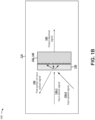
- a similar example implementation 100' includes a set of sensor elements of a sensor element array 140 is integrated into a substrate 120 of an optical filter structure.
- optical filter 130 is disposed onto substrate 120.
- Input optical signals 150-1 and 150-2 are received at a set of angles and a first portion of input optical signals 150-1 and 150-2 is reflected at another set of angles.
- a second portion of input optical signals 150-1 and 150-2 is passed through optical filter 130 to sensor element array 140, which provides an output electrical signal 180.
- another similar example implementation 100" includes a set of sensor elements of a sensor element array 140 separated from an optical filter structure 120, and optical filter 130 is disposed onto optical filter structure 130.
- optical filter structure 130 and sensor element array 140 may be separated by free space or the like.
- Input optical signals 150-1 and 150-2 are received at a set of angles at optical filter 130.
- a first portion 160 of the input optical signals 150-1 and 150-2 is reflected and a second portion 170 is passed by optical filter 130 and optical filter structure 120 to sensor element array 140, which provides an output electrical signal 180.
- FIGS. 1A-1C are provided merely as examples. Other examples are possible and may differ from what was described with regard to Figs. 1A-1C .
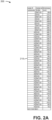
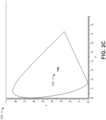
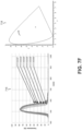
- Figs. 2A-2C are diagrams of characteristics relating to an optical filter. Figs. 2A-2C show an example of an all-dielectric filter.
- a filter 210 may include a substrate and a set of dielectric stacks.
- the substrate may include a silicon nitride (Si 3 N 4 and shown as Si3N4), a glass substrate, a polymer substrate, another transparent substrate, or the like.
- the substrate may be attached to the set of dielectric stacks using an epoxy (e.g., a transparent glue), an air gap (e.g., with an epoxy outside of an optical path), or the like.
- the set of dielectric stacks may be disposed directly onto a detector, detector array, sensor element array, or the like, which may form the substrate for the set of dielectric stacks.
- a sensor element array may include a top layer of silicon nitride to which the set of dielectric stacks may be attached.
- another type of substrate may be used, such as a silicon substrate.
- the substrate may be an entrance medium, an exit medium, or the like for the set of dielectric stacks.
- the set of dielectric stacks includes alternating layers of niobium titanium oxide (NbTiO 5 and shown as NbTiO5) and silicon dioxide (SiO 2 and shown as SiO2).
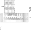
- filter 210 may include a first niobium titanium oxide layer with a thickness of 99.8 nanometers (nm) deposited onto the substrate and a first silicon dioxide layer with a thickness of 172.1 nm deposited onto the niobium titanium oxide layer.
- filter 210 may include a second niobium titanium oxide layer deposited with a thickness of 105.2 nm deposited onto the first silicon dioxide layer and a second silicon dioxide layer with a thickness of 180.5 nm deposited onto the second niobium titanium oxide layer.
- filter 210 is associated with a total thickness of approximately 5.36 micrometers ( ⁇ m), which may result in excessive deposition time and excessive cost relating to the increased deposition time.
- the total thickness may result in a threshold amount of compressive stress, which may result in a warping of a substrate with less than a threshold thickness and which may result in excessive difficulty and yield loss when portioning a substrate onto which multiple filters are deposited to form multiple, discrete filters.
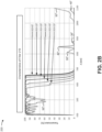
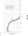
- filter 210 is associated with a cut-off wavelength (e.g., a wavelength at which a transmissivity of filter 210 reduces at a threshold rate) of approximately 660 nm at an angle of incidence (AOI) of 0 degrees.
- AOI angle of incidence
- filter 210 is associated with a threshold shift in the cut-off wavelength of approximately 5 nm, approximately 12 nm, approximately 25 nm, approximately 42 nm, and approximately 52 nm, respectively.
- filter 210 is associated with a transmissivities of approximately 4% at approximately 880 nm, approximately 31% at approximately at approximately 850 nm, and approximately 14% at approximately 805 nm, respectively.
- filter 210 is associated with a drop in transmissivity to below a threshold transmissivity (e.g., to a transmissivity of between approximately 58% and approximately 68%) between approximately 480 nm and approximately 505 nm at an AOI of 50 degrees, and filter 210 is associated with an increase in transmissivity to greater than a threshold transmissivity (e.g., to a transmissivity greater than approximately 1%) at a spectral range greater than approximately 1000 nm for the AOI of 50 degrees.
- a threshold transmissivity e.g., to a transmissivity of between approximately 58% and approximately 68%
- filter 210 is associated with an increase in transmissivity to greater than a threshold transmissivity (e.g., to a transmissivity greater than approximately 1%) at a spectral range greater than approximately 1000 nm for the AOI of 50 degrees.
- the threshold angle shifts and the threshold transmissivity drops and increases result in relatively poor filter performance.
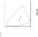
- a color plot for filter 210 is provided (e.g., an International Commission on Illumination (CIE) 1931 color plot).
- CIE International Commission on Illumination
- filter 210 is associated with a CIE color plot indicating a threshold color shift between approximately (0.33, 0.33) to approximately (0.30, 0.33) at a shift from a 0 degree AOI to a 50 degree AOI.
- the threshold color shift results in relatively poor filter performance.
- FIGS. 2A-2C are provided merely as examples. Other examples are possible and may differ from what was described with regard to Figs. 2A-2C .
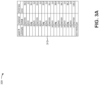
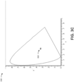
- Figs. 3A-3C are diagrams of characteristics relating to an optical filter.
- Figs. 3A-3C show an example of a low angle shift induced transmission optical filter (TTF) with dielectric/metal filter stacks.
- TTF transmission optical filter
- a filter 310 may include a substrate, a set of dielectric layers, and a set of metal layers.
- the substrate may include a silicon nitride substrate.
- the set of dielectric layers and the set of metal layers include alternating layers of niobium titanium oxide, zinc oxide (ZnO), and silver (Ag).
- a first layer of niobium titanium oxide with a thickness of 28.0 nm is deposited onto a silicon nitride substrate, a second layer of zinc oxide with a thickness of 2.0 nm is deposited onto the first layer, a third layer of silver with a thickness of 11.3 nm is deposited onto the second layer, a fourth layer of zinc oxide with a thickness of 2.0 nm is deposited onto the third layer, and a fifth layer of niobium titanium oxide with a thickness of 53.8 nm is deposited onto the fourth layer.
- the fifth layer of niobium titanium oxide may be multiple layers of niobium titanium oxide.
- a first portion of the fifth layer may be to sandwich the second layer through the fourth layer with the first layer, and a second portion of the fifth layer may be to sandwich a sixth layer through an eighth layer with a portion of a ninth layer.
- filter 310 is described with a particular set of layer thicknesses, other layer thicknesses are possible and may differ from what is shown in Fig. 3A .
- filter 310 is associated with a reduced angle shift relative to filter 210.
- filter 310 is associated with an angle shift of a cutoff wavelength of less than approximately 20 nm for a change in angle of incidence from 0 degrees to 10 degrees, 20 degrees, 30 degrees, 40 degrees, or 50 degrees compared with an angle shift of great than 20 nm for a change in angle of incidence from 0 degrees to 30 degrees, 40 degrees, or 50 degrees.
- filter 310 is associated with a reduced transmissivity relative to filter 210.
- filter 310 is associated with an average transmissivity of between approximately 62% and 65% for angles of incidence between 0 degrees and 50 degrees in a spectral range of the passband of between approximately 420 nm and approximately 620 nm.
- a transmissivity in an infrared (IR) blocking spectral range of approximately 750 nm to approximately 1100 nm is approximately 0.41% for an AOI of 0 degrees and approximately 0.37% for an AOI of 40 degrees.
- filter 310 is associated with a reduced color shift relative to filter 210 for a shift from a 0 degree angle of incidence to a 50 degree angle of incidence.
- filter 310 is associated with a color shift less than a threshold (e.g., less than 0.2, less than 0.1, less than 0.05, etc.).
- FIGS. 3A-3C are provided merely as examples. Other examples are possible and may differ from what was described with regard to Figs. 3A-3C .
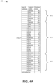
- Figs. 4A-4C are a diagram of characteristics relating to a mixed metal/dielectric optical filter.
- Figs. 4A-4C show an example of an optical filter with dielectric filter stacks of high-index layers and low-index layers and with a metal (e.g., silver) dielectric filter stack disposed between the dielectric filter stacks.
- a metal e.g., silver
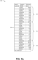
- a filter 410 may include a substrate, a set of dielectric layers, and a set of metal layers.
- a first portion of filter 410 (e.g., a first all-dielectric portion) includes all-dielectric layers of alternating high-index layers and low-index layers.
- the alternating high-index layers and low-index layers are, respectively, niobium titanium oxide layers and silicon dioxide layers.
- a first layer deposited onto the silicon nitride substrate is a niobium titanium oxide layer with a thickness of 95.5 nm (shown as layer 1)
- a second layer deposited onto the first layer is silicon dioxide with a thickness of 48.3 nm (shown as layer 2)
- another type of substrate may be used, such as a glass substrate or the like.
- another high-index material may be used, such as a material with a refractive index greater than approximately 2.0, greater than approximately 2.5, greater than approximately 3.0, greater than approximately 3.5, greater than approximately 3.6, greater than approximately 3.7, etc.
- another low-index material may be used, such as a material with a refractive index less than approximately 3.0, less than approximately 2.5, less than approximately 2.0, less than approximately 1.5, etc.
- one or more layers may utilize, as a dielectric material, an oxide material, such as silicon dioxide (SiO 2 ), niobium pentoxide (Nb 2 O 5 ), tantalum pentoxide (Ta 2 O 5 ), titanium dioxide (TiO 2 ), aluminum oxide (Al 2 O 3 ), zirconium oxide (ZrO 2 ), yttrium oxide (Y 2 O 3 ), hafnium dioxide (HfO 2 ), or the like; a nitride material, such as silicon nitride (Si3N4); a fluoride material, such as magnesium fluoride (MgF); a sulfide material, such as zinc sulfide (ZnS); a selenide material, such as zinc selenide (Zn
- a second portion of filter 410 includes mixed metal/dielectric layers.
- the second portion of filter 410 includes multiple layer groups of one or more niobium titanium oxide layers, one or more zinc oxide layers, and one or more silver layers.
- a first layer group includes a layer of niobium titanium oxide with a thickness of 139.1 nm (e.g., shown as layer 7, a first portion of which may be a part of the first portion of filter 410 and a second portion of which may be a part of the second portion of filter 410), a layer of zinc oxide with a thickness of 2.0 nm (shown as layer 8), a layer of silver with a thickness of 9.9 nm (shown as layer 9), a layer of zinc oxide with a thickness of 2.0 nm (shown as layer 10), and a layer of niobium titanium oxide with a thickness of 51.9 nm (shown as layer 11, a first portion of which may be a part of the first layer group, a second portion of which may be a part of a second layer group).
- a second layer group includes the second portion of layer 11 of niobium titanium oxide, layer 12 of zinc oxide, layer 13 of silver, layer 14 of zinc oxide, and a first portion of layer 15 of niobium titanium oxide (e.g., a second portion of which may be part of a third layer group).
- a first portion of layer 15 of niobium titanium oxide e.g., a second portion of which may be part of a third layer group.
- another metal material may be utilized.
- a third portion of filter 410 includes all-dielectric layers of alternating high-index layers and low-index layers.
- the alternating high-index layers and low-index layers are, respectively, niobium titanium oxide layers and silicon dioxide layers.
- a first layer is a portion of layer 23 of niobium titanium oxide
- a second layer is layer 24 of silicon dioxide
- a third layer is layer 25 of niobium titanium oxide
- a fourth layer is layer 26 of silicon dioxide, etc.
- filter 410 utilizes three different dielectric materials.
- filter 410 may utilize two different dielectric materials.
- filter 410 may be matched to an exit medium of air. In some implementations, filter 410 may be matched to another exit medium, such as a polymer material, a color dye, an RGB dye, an epoxy material, a glass material, or the like. In some implementations, filter 410 may be an RGB filter (e.g., a filter with a passband corresponding to a red spectral range of light, a green spectral range of light, or a blue spectral range of light), an NIR blocker, an LWP filter, an SWP filter, a photopic filter, an ambient light sensor filter, a tri-stimulus filter, or the like.
- filter 410 is described with a particular set of layer thicknesses, other layer thicknesses are possible and may differ from what is shown in Fig. 4A .
- filter 410 is associated with a reduced angle shift and color shift relative to filter 210 and an improved transmissivity relative to filter 310.
- filter 410 is associated with a transitivity of approximately 80% at approximately 420 nm and an angle of incidence of 0 degrees, and is associated with a transmissivity greater than 70% for a spectral range of between approximately 420 nm and 550 nm for angles of incidence of between 0 degrees and 50 degrees.
- filter 410 is associated with an angle shift of less than approximately 40 nm for the spectral range of between approximately 400 nm and approximately 1100 nm and angles of incidence between 0 degrees and 50 degrees.
- filter 410 is associated with a reduced color shift relative to filter 210 for a shift from a 0 degree angle of incidence to a 50 degree angle of incidence.
- filter 410 is associated with a color shift less than a threshold (e.g., less than 0.2, less than 0.1, less than 0.05, etc.).
- FIGS. 4A-4C are provided merely as examples. Other examples are possible and may differ from what was described with regard to Figs. 4A-4C .
- Figs. 5A-5C are a diagram of characteristics relating to another mixed metal/dielectric optical filter.
- Figs. 5A-5C show another example of an induced transmission optical filter with dielectric filter stacks of high-index layers and low-index layers and with metal (e.g., silver) dielectric filter stacks.
- a filter 510 may include a substrate, a set of dielectric layers, and a set of metal layers.
- a first portion of filter 510, of layers 1 to 10 includes all-dielectric layers of alternating high-index layers and low-index layers.
- the alternating high-index layers and low-index layers are, respectively, niobium titanium oxide layers and silicon dioxide layers.
- a second portion of filter 510, of layers 10 to 25 includes metal dielectric layers.
- the second portion of filter 510 includes multiple layer groups of one or more niobium titanium oxide layers, one or more zinc oxide layers, and one or more silver layers.
- a third portion of filter 510 includes all-dielectric layers of alternating high-index layers and low-index layers.
- the alternating high-index layers and low-index layers are, respectively, niobium titanium oxide layers and silicon dioxide layers.
- filter 510 is described with a particular set of layer thicknesses, other layer thicknesses are possible and may differ from what is shown in Fig. 5A .
- filter 510 is associated with a reduced angle shift and color shift relative to filter 210 and an improved transmissivity relative to filter 310.
- filter 510 is associated with a transitivity of approximately 80% at approximately 500 nm and at angles of incidence of 0 degrees to 50 degrees, and is associated with a transmissivity greater than approximately 70% for a spectral range of between approximately 460 nm and 590 nm at angles of incidence between 0 degrees and 50 degrees.
- filter 510 is associated with an angle shift of less than approximately 30 nm for the spectral range of between approximately 400 nm and approximately 1100 nm and angles of incidence between 0 degrees and 50 degrees.
- filter 510 is associated with a reduced color shift relative to filter 210 for a shift from a 0 degree angle of incidence to a 50 degree angle of incidence.
- filter 510 is associated with a color shift less than a threshold (e.g., less than 0.2, less than 0.1, less than 0.05, etc.).
- FIGS. 5A-5C are provided merely as examples. Other examples are possible and may differ from what was described with regard to Figs. 5A-5C .
- Figs. 6A and 6B are diagrams of characteristics relating to a set of optical filters. Figs. 6A and 6B show a comparison of characteristics of filters described herein.
- filter 410 and filter 510 are associated with a reduced angle shift of the cut-off wavelength relative to filter 210 at each angle of incidence from 0 degrees to 50 degrees.
- filter 410 is associated with an angle shift of a cut-off wavelength of approximately 18 nm.
- filter 510 is associated with an angle shift of a cut-off wavelength of approximately 20 nm.
- filter 210 is associated with a change in a cut-off wavelength of approximately 42 nm.
- a comparison of average transmissivity of a passband of a spectral range of approximately 420 nm to approximately 620 nm for filter 210, filter 310, filter 410, and filter 510 is provided.
- filter 410 and filter 510 are associated with an improved transmissivity relative to filter 310.
- At each angle of incidence from 0 degrees to 50 degrees.
- filter 410 and filter 510 are associated with an average transmissivity of approximately 72% and approximately 75%, respectively.
- filter 310 is associated with an average transmissivity of approximately 63%.
- FIGS. 6A and 6B are provided merely as examples. Other examples are possible and may differ from what was described with regard to Figs. 6A and 6B .
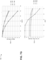
- Figs. 7A-7G are diagrams of characteristics relating to a set of optical filters. Figs. 7A-7G show a comparison of characteristics of green color types of filters described herein.
- Filter 702 may be a green color filter that includes alternating layers of silicon dioxide (SiO 2 ) and niobium titanium oxide (NbTiOs). Filter 702 may be associated with an entrance medium of silicon nitride (Si 3 N 4 ) and an exit medium of air. Filter 702 may be an all-dielectric type of filter, and may be similar to filter 210, shown in Fig. 2A .
- Filter 704 may be a green color filter that includes layers of niobium titanium oxide (NbTiOs), zinc oxide (ZnO), and silver (Ag), an entrance medium of silicon nitride (Si 3 N 4 ), and an exit medium of air. Filter 704 may be similar to filter 310, shown in Fig. 3A .
- Filter 706 may be a green color filter that includes layers of niobium titanium oxide (NbTiOs), silicon dioxide (SiO 2 ), zinc oxide (ZnO), and silver (Ag), an entrance medium of silicon nitride (Si 3 N 4 ), and an exit medium of air.
- Filter 706 may be similar to filter 410 shown in Fig. 4A .
- filter 706 may include a first portion, such as layers 1 through 13, that includes alternating dielectric layers; a second portion, such as layers 13 to 25, that includes alternating dielectric layers and metal layers; and a third portion, such as layers 25 to 37, that includes alternating dielectric layers.
- filter 702 is associated with an angle shift for a change in angle of incidence (AOI) from approximately 0 degrees to approximately 50 degrees of between approximately 50 nm and approximately 80 nm for a spectral range of between approximately 450 nm and approximately 575 nm.
- AOI angle of incidence
- filter 702 is associated with a drop in peak transmission in a passband from approximately 100% at an angle of incidence of approximately 0 degrees to approximately 90% at an angle of incidence of approximately 50 degrees.
- filter 702 is associated with a color shift in a CIE 1931 color plot from approximately [0.08, 0.47] to approximately [0.25, 0.69].
- filter 704 is associated with an angle shift for a change in angle of incidence (AOI) from approximately 0 degrees to approximately 50 degrees of between approximately 25 nm and approximately 40 nm for a spectral range of between approximately 450 nm and approximately 575 nm.
- AOI angle of incidence
- filter 704 is associated with a drop in peak transmission in a passband from approximately 72% at an angle of incidence of approximately 0 degrees to approximately 66% at an angle of incidence of approximately 50 degrees.
- filter 704 is associated with a color shift in a CIE 1931 color plot from approximately [0.17, 0.58] to approximately [0.26, 0.63].
- filter 706 is associated with an angle shift for a change in angle of incidence (AOI) from approximately 0 degrees to approximately 50 degrees of between approximately 25 nm and approximately 40 nm for a spectral range of between approximately 450 nm and approximately 575 nm.
- AOI angle of incidence
- filter 706 is associated with a drop in peak transmission in a passband from approximately 78% at an angle of incidence of approximately 0 degrees to approximately 70% at an angle of incidence of approximately 50 degrees.
- filter 706 is associated with a color shift in a CIE 1931 color plot from approximately [0.18, 0.62] to approximately [0.26, 0.65]. In this way, filter 706 is associated with a reduced angle shift and a reduced color shift relative to filter 702 and an improved transmissivity relative to filter 704.
- a comparison of change in center wavelength and a comparison in average transmission in a passband of approximately 510 nm to approximately 550 is provided, respectively, for filter 702, filter 704, and filter 706.
- filter 706 is associated with a reduced change in center wavelength relative to filter 702 for angles of incidence of approximately 10 degrees to approximately 50 degrees.
- filter 706 is associated with an improved average transmission, in the passband, relative to filter 704 for angles of incidence of approximately 0 degrees to approximately 50 degrees, and an improved average transmission relative to filter 706 for angles of incidence, in the passband, from approximately 40 degrees to approximately 50 degrees.
- FIGS. 7A-7G are provided merely as examples. Other examples are possible and may differ from what was described with regard to Figs. 7A-7G .
- a filter that includes a first portion of dielectric layers, a second portion of mixed dielectric and metal layers, and a third portion of dielectric layers provides filtering with a reduced angle shift and improved transmissivity relative to an all-dielectric filter or LAS ITF filter. Based on reducing an angle shift and improving a transmissivity, an accuracy of data obtained by a sensor element aligned to the filter is improved relative to an accuracy of data obtained by a sensor element aligned to another type of filter.
- satisfying a threshold may refer to a value being greater than the threshold, more than the threshold, higher than the threshold, greater than or equal to the threshold, less than the threshold, fewer than the threshold, lower than the threshold, less than or equal to the threshold, equal to the threshold, etc.
Landscapes
- Physics & Mathematics (AREA)
- General Physics & Mathematics (AREA)
- Optics & Photonics (AREA)
- Chemical & Material Sciences (AREA)
- Engineering & Computer Science (AREA)
- Power Engineering (AREA)
- Inorganic Chemistry (AREA)
- Microelectronics & Electronic Packaging (AREA)
- Electromagnetism (AREA)
- Condensed Matter Physics & Semiconductors (AREA)
- Computer Hardware Design (AREA)
- Ceramic Engineering (AREA)
- Chemical Kinetics & Catalysis (AREA)
- Metallurgy (AREA)
- Materials Engineering (AREA)
- Organic Chemistry (AREA)
- Mechanical Engineering (AREA)
- Optical Filters (AREA)
- Solid State Image Pick-Up Elements (AREA)
- Laminated Bodies (AREA)
- Surface Treatment Of Glass (AREA)
- Glass Compositions (AREA)
Applications Claiming Priority (2)
| Application Number | Priority Date | Filing Date | Title |
|---|---|---|---|
| US15/601,773 US10451783B2 (en) | 2017-05-22 | 2017-05-22 | Induced transmission filter having plural groups of alternating layers of dielectric material for filtering light with less than a threshold angle shift |
| EP18170860.3A EP3407103B1 (en) | 2017-05-22 | 2018-05-04 | Induced transmission filter |
Related Parent Applications (3)
| Application Number | Title | Priority Date | Filing Date |
|---|---|---|---|
| EP18170860.3A Division-Into EP3407103B1 (en) | 2017-05-22 | 2018-05-04 | Induced transmission filter |
| EP18170860.3A Division EP3407103B1 (en) | 2017-05-22 | 2018-05-04 | Induced transmission filter |
| EP18170860.3A Previously-Filed-Application EP3407103B1 (en) | 2017-05-22 | 2018-05-04 | Induced transmission filter |
Publications (2)
| Publication Number | Publication Date |
|---|---|
| EP4400876A2 true EP4400876A2 (en) | 2024-07-17 |
| EP4400876A3 EP4400876A3 (en) | 2024-09-25 |
Family
ID=62222385
Family Applications (2)
| Application Number | Title | Priority Date | Filing Date |
|---|---|---|---|
| EP18170860.3A Active EP3407103B1 (en) | 2017-05-22 | 2018-05-04 | Induced transmission filter |
| EP24177928.9A Pending EP4400876A3 (en) | 2017-05-22 | 2018-05-04 | Induced transmission filter |
Family Applications Before (1)
| Application Number | Title | Priority Date | Filing Date |
|---|---|---|---|
| EP18170860.3A Active EP3407103B1 (en) | 2017-05-22 | 2018-05-04 | Induced transmission filter |
Country Status (8)
| Country | Link |
|---|---|
| US (5) | US10451783B2 (ko) |
| EP (2) | EP3407103B1 (ko) |
| JP (2) | JP7150464B2 (ko) |
| KR (2) | KR102292755B1 (ko) |
| CN (2) | CN108933150B (ko) |
| CA (1) | CA3003014A1 (ko) |
| HK (2) | HK1256268A1 (ko) |
| TW (4) | TWI849875B (ko) |
Families Citing this family (15)
| Publication number | Priority date | Publication date | Assignee | Title |
|---|---|---|---|---|
| US10647611B2 (en) * | 2017-03-10 | 2020-05-12 | Guardian Glass, LLC | IG window unit having triple silver coating and dielectric coating on opposite sides of glass substrate |
| US10451783B2 (en) | 2017-05-22 | 2019-10-22 | Viavi Solutions Inc. | Induced transmission filter having plural groups of alternating layers of dielectric material for filtering light with less than a threshold angle shift |
| US11215741B2 (en) * | 2018-01-17 | 2022-01-04 | Viavi Solutions Inc. | Angle of incidence restriction for optical filters |
| US11009636B2 (en) * | 2018-03-13 | 2021-05-18 | Viavi Solutions Inc. | Sensor window to provide different opacity and transmissivity at different spectral ranges |
| US10948640B2 (en) | 2018-03-13 | 2021-03-16 | Viavi Solutions Inc. | Sensor window with a set of layers configured to a particular color and associated with a threshold opacity in a visible spectral range wherein the color is a color-matched to a surface adjacent to the sensor window |
| GB201902046D0 (en) | 2019-02-14 | 2019-04-03 | Teledyne E2V Uk Ltd | Biased idf photodetector |
| CN110082849A (zh) * | 2019-06-05 | 2019-08-02 | 信阳舜宇光学有限公司 | 近红外窄带滤光片及制作方法 |
| US11630062B2 (en) * | 2019-10-10 | 2023-04-18 | Visera Technologies Company Limited | Biosensor and method of forming the same |
| US11705472B2 (en) * | 2019-10-10 | 2023-07-18 | Visera Technologies Company Limited | Biosensor and method of distinguishing a light |
| US20210318476A1 (en) * | 2020-04-10 | 2021-10-14 | Viavi Solutions Inc. | Optical filter |
| US20210333454A1 (en) * | 2020-04-28 | 2021-10-28 | Viavi Solutions Inc. | Induced transmission filter with hydrogenated silicon and silver |
| JP7209273B2 (ja) * | 2020-05-29 | 2023-01-20 | パナソニックIpマネジメント株式会社 | フィルタアレイおよび光検出システム |
| JP2023535159A (ja) * | 2020-07-17 | 2023-08-16 | エヴァテック・アーゲー | 生体認証システム |
| US20230012033A1 (en) * | 2021-07-07 | 2023-01-12 | Viavi Solutions Inc. | Multi-bandpass optical interference filter |
| TWI840044B (zh) * | 2022-12-23 | 2024-04-21 | 澤米科技股份有限公司 | 窄帶通濾光元件 |
Family Cites Families (30)
| Publication number | Priority date | Publication date | Assignee | Title |
|---|---|---|---|---|
| CH564785A5 (ko) * | 1972-12-08 | 1975-07-31 | Balzers Patent Beteilig Ag | |
| EP0244394B1 (de) * | 1986-04-23 | 1992-06-17 | AVL Medical Instruments AG | Sensorelement zur Bestimmung von Stoffkonzentrationen |
| US4783696A (en) * | 1986-12-05 | 1988-11-08 | Hewlett-Packard Company | Color image input apparatus with various elements having matched apertures |
| US5337191A (en) | 1993-04-13 | 1994-08-09 | Photran Corporation | Broad band pass filter including metal layers and dielectric layers of alternating refractive index |
| ATE296787T1 (de) * | 1998-12-18 | 2005-06-15 | Glaverbel | Verglasungsscheibe |
| KR100424254B1 (ko) * | 1999-08-06 | 2004-03-22 | 삼성에스디아이 주식회사 | 플라즈마 표시 장치용 광학 필터 |
| US6919133B2 (en) * | 2002-03-01 | 2005-07-19 | Cardinal Cg Company | Thin film coating having transparent base layer |
| JP2004207383A (ja) * | 2002-12-24 | 2004-07-22 | Central Glass Co Ltd | 電磁遮蔽膜 |
| US7133197B2 (en) | 2004-02-23 | 2006-11-07 | Jds Uniphase Corporation | Metal-dielectric coating for image sensor lids |
| US7081302B2 (en) * | 2004-02-27 | 2006-07-25 | Centre Luxembourgeois De Recherches Pour Le Verre Et La Ceramique S.A. (C.R.V.C.) | Coated article with low-E coating including tin oxide interlayer |
| JP2005258050A (ja) | 2004-03-11 | 2005-09-22 | Nippon Sheet Glass Co Ltd | 反射鏡およびそれを用いた画像投影装置 |
| JPWO2006090798A1 (ja) | 2005-02-25 | 2008-07-24 | 旭硝子株式会社 | 電磁波遮蔽積層体およびこれを用いたディスプレイ装置 |
| US20060262389A1 (en) * | 2005-05-23 | 2006-11-23 | Christoph Zaczek | Reflective optical element for ultraviolet radiation, projection optical system and projection exposure system therewith, and method for forming the same |
| JP4765504B2 (ja) * | 2005-09-16 | 2011-09-07 | 東レ株式会社 | 光学フィルタ |
| US7508586B2 (en) * | 2006-04-14 | 2009-03-24 | Southwall Technologies, Inc. | Zinc-based film manipulation for an optical filter |
| US20080258043A1 (en) * | 2007-04-17 | 2008-10-23 | Koji Suzuki | Optical element and optical equipment |
| US7713633B2 (en) * | 2008-05-27 | 2010-05-11 | Guardian Industries Corp. | EMI filter for plasma display panel |
| JP2010032867A (ja) | 2008-07-30 | 2010-02-12 | Enplas Corp | Irカットフィルタ |
| EP2347895A4 (en) * | 2008-11-11 | 2013-02-20 | Asahi Glass Co Ltd | ELECTRICALLY CONDUCTIVE COATING AND PROTECTIVE PLATE FOR A PLASMA INDICATOR |
| US20110291113A1 (en) * | 2010-05-27 | 2011-12-01 | Philips Lumileds Lighting Company, Llc | Filter for a light emitting device |
| KR101553731B1 (ko) * | 2011-04-14 | 2015-09-16 | 충북대학교 산학협력단 | 레이저 검출 장치 및 방법 |
| US10197716B2 (en) | 2012-12-19 | 2019-02-05 | Viavi Solutions Inc. | Metal-dielectric optical filter, sensor device, and fabrication method |
| US9448346B2 (en) | 2012-12-19 | 2016-09-20 | Viavi Solutions Inc. | Sensor device including one or more metal-dielectric optical filters |
| TWI549811B (zh) * | 2013-07-23 | 2016-09-21 | 大立光電股份有限公司 | 紅外線濾光元件 |
| JP6509258B2 (ja) | 2014-06-18 | 2019-05-08 | ヴァイアヴィ・ソリューションズ・インコーポレイテッドViavi Solutions Inc. | 金属誘電体光学フィルター、センサーデバイス、および製造方法 |
| CN104401062B (zh) * | 2014-12-03 | 2017-01-04 | 张家港康得新光电材料有限公司 | 一种窗膜及其制备方法 |
| JP6222413B2 (ja) * | 2015-09-25 | 2017-11-01 | 旭硝子株式会社 | 光学フィルタおよび撮像装置 |
| PE20180980A1 (es) * | 2015-10-13 | 2018-06-19 | Vision Ease Lp | Filtro optico con transmitancia y reflectancia selectivas |
| US10386463B1 (en) * | 2016-12-29 | 2019-08-20 | X Development Llc | Retroreflector with wavelength-dependent response to convey pose information |
| US10451783B2 (en) | 2017-05-22 | 2019-10-22 | Viavi Solutions Inc. | Induced transmission filter having plural groups of alternating layers of dielectric material for filtering light with less than a threshold angle shift |
-
2017
- 2017-05-22 US US15/601,773 patent/US10451783B2/en active Active
-
2018
- 2018-04-27 CA CA3003014A patent/CA3003014A1/en active Pending
- 2018-04-27 JP JP2018087590A patent/JP7150464B2/ja active Active
- 2018-05-01 TW TW112116185A patent/TWI849875B/zh active
- 2018-05-01 TW TW107114783A patent/TWI770168B/zh active
- 2018-05-01 TW TW111123262A patent/TWI793034B/zh active
- 2018-05-01 TW TW111149526A patent/TWI804454B/zh active
- 2018-05-04 EP EP18170860.3A patent/EP3407103B1/en active Active
- 2018-05-04 EP EP24177928.9A patent/EP4400876A3/en active Pending
- 2018-05-21 KR KR1020180057693A patent/KR102292755B1/ko active IP Right Grant
- 2018-05-22 CN CN201810494057.XA patent/CN108933150B/zh active Active
- 2018-05-22 CN CN202110203454.9A patent/CN112768483A/zh active Pending
- 2018-11-29 HK HK18115328.1A patent/HK1256268A1/zh unknown
-
2019
- 2019-01-25 HK HK19101351.0A patent/HK1258878A1/zh unknown
- 2019-10-03 US US16/591,849 patent/US10866347B2/en active Active
-
2020
- 2020-11-25 US US17/247,046 patent/US11340391B2/en active Active
-
2021
- 2021-08-13 KR KR1020210107312A patent/KR102433179B1/ko active IP Right Grant
-
2022
- 2022-05-13 US US17/663,265 patent/US11828963B2/en active Active
- 2022-08-04 JP JP2022124696A patent/JP2022166089A/ja active Pending
-
2023
- 2023-10-27 US US18/495,942 patent/US20240053520A1/en active Pending
Also Published As
Similar Documents
| Publication | Publication Date | Title |
|---|---|---|
| US11340391B2 (en) | Induced transmission filter comprising plural layers associated with an angle shift for a change in angle of incidence | |
| CA2957193C (en) | Fabricating a sensor device | |
| US20230012033A1 (en) | Multi-bandpass optical interference filter | |
| CN110018542A (zh) | 光学滤波器 | |
| US11143803B2 (en) | Multispectral filter | |
| JP7145086B2 (ja) | 光学フィルタ用の入射角制限 | |
| EP4198469A1 (en) | Optical interference filter | |
| EP3893032A2 (en) | Optical filter |
Legal Events
| Date | Code | Title | Description |
|---|---|---|---|
| PUAI | Public reference made under article 153(3) epc to a published international application that has entered the european phase |
Free format text: ORIGINAL CODE: 0009012 |
|
| STAA | Information on the status of an ep patent application or granted ep patent |
Free format text: STATUS: THE APPLICATION HAS BEEN PUBLISHED |
|
| AC | Divisional application: reference to earlier application |
Ref document number: 3407103 Country of ref document: EP Kind code of ref document: P |
|
| AK | Designated contracting states |
Kind code of ref document: A2 Designated state(s): AL AT BE BG CH CY CZ DE DK EE ES FI FR GB GR HR HU IE IS IT LI LT LU LV MC MK MT NL NO PL PT RO RS SE SI SK SM TR |
|
| PUAL | Search report despatched |
Free format text: ORIGINAL CODE: 0009013 |
|
| AK | Designated contracting states |
Kind code of ref document: A3 Designated state(s): AL AT BE BG CH CY CZ DE DK EE ES FI FR GB GR HR HU IE IS IT LI LT LU LV MC MK MT NL NO PL PT RO RS SE SI SK SM TR |
|
| RIC1 | Information provided on ipc code assigned before grant |
Ipc: G02B 5/28 20060101AFI20240822BHEP |