EP4397791A1 - Coating structure comprising graphite composite and preparation method - Google Patents
Coating structure comprising graphite composite and preparation method Download PDFInfo
- Publication number
- EP4397791A1 EP4397791A1 EP23215205.8A EP23215205A EP4397791A1 EP 4397791 A1 EP4397791 A1 EP 4397791A1 EP 23215205 A EP23215205 A EP 23215205A EP 4397791 A1 EP4397791 A1 EP 4397791A1
- Authority
- EP
- European Patent Office
- Prior art keywords
- layer
- graphite
- alloy layer
- metal
- alloy
- Prior art date
- Legal status (The legal status is an assumption and is not a legal conclusion. Google has not performed a legal analysis and makes no representation as to the accuracy of the status listed.)
- Pending
Links
Images

Classifications
-
- C—CHEMISTRY; METALLURGY
- C25—ELECTROLYTIC OR ELECTROPHORETIC PROCESSES; APPARATUS THEREFOR
- C25D—PROCESSES FOR THE ELECTROLYTIC OR ELECTROPHORETIC PRODUCTION OF COATINGS; ELECTROFORMING; APPARATUS THEREFOR
- C25D15/00—Electrolytic or electrophoretic production of coatings containing embedded materials, e.g. particles, whiskers, wires
-
- C—CHEMISTRY; METALLURGY
- C25—ELECTROLYTIC OR ELECTROPHORETIC PROCESSES; APPARATUS THEREFOR
- C25D—PROCESSES FOR THE ELECTROLYTIC OR ELECTROPHORETIC PRODUCTION OF COATINGS; ELECTROFORMING; APPARATUS THEREFOR
- C25D3/00—Electroplating: Baths therefor
- C25D3/02—Electroplating: Baths therefor from solutions
- C25D3/56—Electroplating: Baths therefor from solutions of alloys
-
- C—CHEMISTRY; METALLURGY
- C25—ELECTROLYTIC OR ELECTROPHORETIC PROCESSES; APPARATUS THEREFOR
- C25D—PROCESSES FOR THE ELECTROLYTIC OR ELECTROPHORETIC PRODUCTION OF COATINGS; ELECTROFORMING; APPARATUS THEREFOR
- C25D3/00—Electroplating: Baths therefor
- C25D3/02—Electroplating: Baths therefor from solutions
- C25D3/56—Electroplating: Baths therefor from solutions of alloys
- C25D3/567—Electroplating: Baths therefor from solutions of alloys containing more than 50% by weight of platinum group metals
-
- C—CHEMISTRY; METALLURGY
- C25—ELECTROLYTIC OR ELECTROPHORETIC PROCESSES; APPARATUS THEREFOR
- C25D—PROCESSES FOR THE ELECTROLYTIC OR ELECTROPHORETIC PRODUCTION OF COATINGS; ELECTROFORMING; APPARATUS THEREFOR
- C25D3/00—Electroplating: Baths therefor
- C25D3/02—Electroplating: Baths therefor from solutions
- C25D3/56—Electroplating: Baths therefor from solutions of alloys
- C25D3/60—Electroplating: Baths therefor from solutions of alloys containing more than 50% by weight of tin
-
- C—CHEMISTRY; METALLURGY
- C25—ELECTROLYTIC OR ELECTROPHORETIC PROCESSES; APPARATUS THEREFOR
- C25D—PROCESSES FOR THE ELECTROLYTIC OR ELECTROPHORETIC PRODUCTION OF COATINGS; ELECTROFORMING; APPARATUS THEREFOR
- C25D5/00—Electroplating characterised by the process; Pretreatment or after-treatment of workpieces
- C25D5/10—Electroplating with more than one layer of the same or of different metals
-
- C—CHEMISTRY; METALLURGY
- C25—ELECTROLYTIC OR ELECTROPHORETIC PROCESSES; APPARATUS THEREFOR
- C25D—PROCESSES FOR THE ELECTROLYTIC OR ELECTROPHORETIC PRODUCTION OF COATINGS; ELECTROFORMING; APPARATUS THEREFOR
- C25D5/00—Electroplating characterised by the process; Pretreatment or after-treatment of workpieces
- C25D5/10—Electroplating with more than one layer of the same or of different metals
- C25D5/12—Electroplating with more than one layer of the same or of different metals at least one layer being of nickel or chromium
-
- C—CHEMISTRY; METALLURGY
- C25—ELECTROLYTIC OR ELECTROPHORETIC PROCESSES; APPARATUS THEREFOR
- C25D—PROCESSES FOR THE ELECTROLYTIC OR ELECTROPHORETIC PRODUCTION OF COATINGS; ELECTROFORMING; APPARATUS THEREFOR
- C25D5/00—Electroplating characterised by the process; Pretreatment or after-treatment of workpieces
- C25D5/10—Electroplating with more than one layer of the same or of different metals
- C25D5/12—Electroplating with more than one layer of the same or of different metals at least one layer being of nickel or chromium
- C25D5/14—Electroplating with more than one layer of the same or of different metals at least one layer being of nickel or chromium two or more layers being of nickel or chromium, e.g. duplex or triplex layers
-
- C—CHEMISTRY; METALLURGY
- C25—ELECTROLYTIC OR ELECTROPHORETIC PROCESSES; APPARATUS THEREFOR
- C25D—PROCESSES FOR THE ELECTROLYTIC OR ELECTROPHORETIC PRODUCTION OF COATINGS; ELECTROFORMING; APPARATUS THEREFOR
- C25D5/00—Electroplating characterised by the process; Pretreatment or after-treatment of workpieces
- C25D5/16—Electroplating with layers of varying thickness
-
- C—CHEMISTRY; METALLURGY
- C25—ELECTROLYTIC OR ELECTROPHORETIC PROCESSES; APPARATUS THEREFOR
- C25D—PROCESSES FOR THE ELECTROLYTIC OR ELECTROPHORETIC PRODUCTION OF COATINGS; ELECTROFORMING; APPARATUS THEREFOR
- C25D5/00—Electroplating characterised by the process; Pretreatment or after-treatment of workpieces
- C25D5/34—Pretreatment of metallic surfaces to be electroplated
-
- C—CHEMISTRY; METALLURGY
- C25—ELECTROLYTIC OR ELECTROPHORETIC PROCESSES; APPARATUS THEREFOR
- C25D—PROCESSES FOR THE ELECTROLYTIC OR ELECTROPHORETIC PRODUCTION OF COATINGS; ELECTROFORMING; APPARATUS THEREFOR
- C25D5/00—Electroplating characterised by the process; Pretreatment or after-treatment of workpieces
- C25D5/48—After-treatment of electroplated surfaces
-
- C—CHEMISTRY; METALLURGY
- C25—ELECTROLYTIC OR ELECTROPHORETIC PROCESSES; APPARATUS THEREFOR
- C25D—PROCESSES FOR THE ELECTROLYTIC OR ELECTROPHORETIC PRODUCTION OF COATINGS; ELECTROFORMING; APPARATUS THEREFOR
- C25D5/00—Electroplating characterised by the process; Pretreatment or after-treatment of workpieces
- C25D5/54—Electroplating of non-metallic surfaces
-
- C—CHEMISTRY; METALLURGY
- C25—ELECTROLYTIC OR ELECTROPHORETIC PROCESSES; APPARATUS THEREFOR
- C25D—PROCESSES FOR THE ELECTROLYTIC OR ELECTROPHORETIC PRODUCTION OF COATINGS; ELECTROFORMING; APPARATUS THEREFOR
- C25D5/00—Electroplating characterised by the process; Pretreatment or after-treatment of workpieces
- C25D5/54—Electroplating of non-metallic surfaces
- C25D5/56—Electroplating of non-metallic surfaces of plastics
-
- C—CHEMISTRY; METALLURGY
- C25—ELECTROLYTIC OR ELECTROPHORETIC PROCESSES; APPARATUS THEREFOR
- C25D—PROCESSES FOR THE ELECTROLYTIC OR ELECTROPHORETIC PRODUCTION OF COATINGS; ELECTROFORMING; APPARATUS THEREFOR
- C25D5/00—Electroplating characterised by the process; Pretreatment or after-treatment of workpieces
- C25D5/60—Electroplating characterised by the structure or texture of the layers
-
- C—CHEMISTRY; METALLURGY
- C25—ELECTROLYTIC OR ELECTROPHORETIC PROCESSES; APPARATUS THEREFOR
- C25D—PROCESSES FOR THE ELECTROLYTIC OR ELECTROPHORETIC PRODUCTION OF COATINGS; ELECTROFORMING; APPARATUS THEREFOR
- C25D7/00—Electroplating characterised by the article coated
-
- C—CHEMISTRY; METALLURGY
- C25—ELECTROLYTIC OR ELECTROPHORETIC PROCESSES; APPARATUS THEREFOR
- C25D—PROCESSES FOR THE ELECTROLYTIC OR ELECTROPHORETIC PRODUCTION OF COATINGS; ELECTROFORMING; APPARATUS THEREFOR
- C25D9/00—Electrolytic coating other than with metals
- C25D9/04—Electrolytic coating other than with metals with inorganic materials
Definitions
- the coating structure further includes a fifth metal layer and a sixth alloy layer.
- the fifth metal layer is plated on the outside of the fourth alloy layer, and does not include graphite.
- the sixth alloy layer is plated on the outside of the fifth metal layer, and includes an alloy synthesized from graphite and metal.
- the coating structure further includes a metal sealing layer plated on the secondary outer side of the coating structure.
- the second alloy layer and the fourth alloy layer each include: a single layer or multiple stacked layers of an alloy layer synthesized from at least graphite and silver, an alloy layer synthesized from at least graphite and gold, an alloy layer synthesized from at least graphite and tin, an alloy layer synthesized from at least graphite and nickel, an alloy layer synthesized from at least graphite and palladium, an alloy layer synthesized from at least graphite and antimony, and an alloy layer synthesized from at least graphite and bismuth.
- the method further comprises plating a metal sealing layer on the secondary outer side of the coating structure.
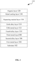
- FIG. 1 shows a schematic diagram of a coating structure according to an embodiment of the present invention.
- the coating structure 100 at least comprises a substrate 102, a first metal layer 104, a second alloy layer 106, a third metal layer 108, and a fourth alloy layer 110.
- the first metal layer 104 is plated on the outside of the substrate 102, and the first metal layer does not include graphite.
- the first metal layer 104 may be pure metal or alloy.
- the first metal layer 104 may include a single layer or multiple stacked layers of a silver layer, a gold layer, a tin layer, a platinum layer, a nickel layer, a palladium layer, a silver alloy layer (such as silver-tin alloy), a gold alloy layer (such as gold-cobalt alloy or goldnickel alloy), a tin alloy layer, a platinum alloy layer, a nickel alloy layer (such as nickelphosphorus alloy), and a palladium alloy layer (such as palladium-nickel alloy).
- the first metal layer 104 may be a silver layer, a silver layer and a gold layer in a stack, or a silver layer and a silver-tin alloy layer in a stack.
- a second alloy layer 106 is plated on the outside of the first metal layer 104, and the second alloy layer 106 includes an alloy synthesized from graphite and metal.
- the second alloy layer 106 includes a single layer or multiple stacked layers of an alloy layer synthesized from at least graphite and silver (such as silver graphite or silver-tin graphite), an alloy layer synthesized from at least graphite and gold (such as gold graphite or gold-cobalt graphite), an alloy layer synthesized from at least graphite and tin (such as tin graphite), an alloy layer synthesized from at least graphite and nickel (such as nickel graphite or palladium-nickel graphite), an alloy layer synthesized from at least graphite and palladium (such as silver-palladium graphite), an alloy layer synthesized from at least graphite and antimony, and an alloy layer synthesized from at least graphite and bismuth.
- the second alloy layer 106 may be a silver-tin graphite layer, or a silver graphite layer and a tin graphite layer in a stack.
- the first metal layer 104 can provide a structure similar to the second alloy layer 106 for plating and reducing face tension, so that the second alloy layer 106 can be closely combined with the first metal layer 104.
- the arrangement of the first metal layer 104 can solve the problem of weak adhesive when the graphite alloy is combined directly with the substrate 102.
- the fourth alloy layer 110 is plated on the outside of the third metal layer 108, and the fourth alloy layer 110 includes an alloy synthesized from graphite and metal.
- the arrangement of the fourth alloy layer 110 is similar to that of the second alloy layer 106.
- the fourth alloy layer 110 may include a single layer or multiple stacked layers of an alloy layer synthesized from at least graphite and silver, an alloy layer synthesized from at least graphite and gold, an alloy layer synthesized from at least graphite and tin, an alloy layer synthesized from at least graphite and nickel, an alloy layer synthesized from at least graphite and palladium, an alloy layer synthesized from at least graphite and antimony, and an alloy layer synthesized from at least graphite and bismuth.
- the coating structure 100 may include a fifth metal layer 112.
- the fifth metal layer 112 is plated on the outside of the fourth alloy layer 110, and the fifth metal layer 112 does not include graphite.
- the arrangement of the fifth metal layer 112 is similar to that of the first metal layer 104.
- the coating structure 100 may include a sixth alloy layer 114.
- the sixth alloy layer 114 is plated on the outside of the fifth metal layer 112, and the sixth alloy layer 114 includes an alloy synthesized from graphite and metal.
- the arrangement of the sixth alloy layer 114 is similar to that of the second alloy layer 106.
- the coating structure 100 further includes an organic layer 120.
- the organic layer 120 is covered on the outermost side of the coating structure 100, which may be sealing agent or lubricating oil, etc.
- Step S202 a first metal layer 104 is plated on the outside of the substrate 102, wherein the first metal layer 104 does not include graphite.
- the first metal layer 104 is obtained by flash plating.
- other metal plating techniques such as chemical plating and hot dipping can also be used to obtain the first metal layer 104.
- Step S204 colloid including graphite is mixed with electroplating solution including second metal ions.
- graphite particles are added to colloid including Sn 2+ and Pd 2+ and well stirred, to obtain the colloid including graphite.
- an acidic colloidal solution of stannous chloride and palladium chloride is firstly prepared, and then anionic dispersant such as sodium hexametaphosphate or sodium stannate is added to mix with the solution to obtain a homogeneous and stable colloid.
- anionic dispersant such as sodium hexametaphosphate or sodium stannate is added to mix with the solution to obtain a homogeneous and stable colloid.
- Sn 2+ is added to colloid palladium, wherein the concentrations of Sn 2+ and Pd 2+ are adjusted.
- Step S206 the mixed electroplating solution including the second metal ions is used to be electrodeposited on the outside of the first metal layer 104, to obtain a second alloy layer 106 synthesized from graphite and the second metal.
- the second metal ions namely Ag + and Sn 2+
- graphite are deposited together on the outside of the first metal layer 104, thereby obtaining the second alloy layer 106 of silver-tin graphite.
- Step S208 ultrasonic water cleaning is used to remove graphite particles on the surface of the second alloy layer 106.
- step S210 that a third metal layer 108 is plated on the outside of the second alloy layer 106, wherein the third metal layer 108 does not include graphite.
- the execution of this step can be referred to step S202.
- step S214 that the mixed electroplating solution including the fourth metal ions is used to be electrodeposited on the outside of the third metal layer 108, to obtain a fourth alloy layer 110 synthesized from graphite and the fourth metal.
- the execution of this step can be referred to step S206.
- step S216 that ultrasonic water cleaning is used to remove graphite particles on a surface of the fourth alloy layer 110.
- the execution of this step can be referred to step S208.
- step S218 that a metal sealing layer 118 is plated on the secondary outer side of the coating structure 100.
Landscapes
- Chemical & Material Sciences (AREA)
- Engineering & Computer Science (AREA)
- Chemical Kinetics & Catalysis (AREA)
- Electrochemistry (AREA)
- Materials Engineering (AREA)
- Metallurgy (AREA)
- Organic Chemistry (AREA)
- Inorganic Chemistry (AREA)
- Laminated Bodies (AREA)
- Electroplating Methods And Accessories (AREA)
- Other Surface Treatments For Metallic Materials (AREA)
- Paints Or Removers (AREA)
Abstract
The present invention provides a coating structure. The coating structure comprises a substrate, a first metal layer, a second alloy layer, a third metal layer, and a fourth alloy layer. The first metal layer is plated on the outside of the substrate, and does not include graphite. The second alloy layer is plated on the outside of the first metal layer, and includes an alloy synthesized from graphite and metal. The third metal layer is plated on the outside of the second alloy layer, and does not include graphite. The fourth alloy layer is plated on the outside of the third metal layer, and includes an alloy synthesized from graphite and metal. By arranging the metal layers without graphite and the alloy layers with graphite to be repeated in a stack, the coating structure can be arranged to any desired thickness, and seal graphite alloy within its structure, thereby preventing graphite particles from floating in the air. Furthermore, the present invention further provides a preparation method for a coating structure.
Description
- The present disclosure relates to electroplating field, more particularly to a coating structure comprising graphite alloy and a preparation method.
- Various metal coatings are widely used on components for electronics, healthcare, locomotives, aviation, and navigation. With the rapid development of the performance of components, people have more demanding requirements for electrical conductivity, thermal conductivity, wear resistance, corrosion resistance, and solderability performances, etc., of metal coating. It has been found that using graphite alloy to manufacture coating can increase its lubricity and wear resistance, resulting in a lower friction coefficient with improved electrical conductivity, thermal conductivity, and wear resistance properties.
- However, the non-polarity of graphite makes it non-hydrophilic, and during the preparation process of graphite alloy, it is easy for graphite to separate and precipitate. This results in an uneven distribution of graphite in the coating. Graphite is prone to be distributed in the superficial layer of the coating, and adhesion of the coating decreases as the content of graphite increases. The deposition quality and efficiency of the coating are not high. Moreover, as graphite partially precipitates during the preparation process, free graphite dust can be harmful to human health. People who inhale it for a long time may suffer allergic asthma and dust-related diseases. Current methods for preparing graphite alloy have other drawbacks, such as a narrow working window for plating solution, limited thickness of coating, and difficulty in industrial mass production.
- To solve the problem above, the present invention proposes a coating structure that seals the graphite alloy inside its structure, which can prevent the graphite particles in the coating from floating in the air.
- Based on that, a coating structure is provided according to an embodiment of the present invention. The coating structure comprises a substrate, a first metal layer, a second alloy layer, a third metal layer, and a fourth alloy layer. The first metal layer is plated on the outside of the substrate, and does not include graphite. The second alloy layer is plated on the outside of the first metal layer, and includes an alloy synthesized from graphite and metal. The third metal layer is plated on the outside of the second alloy layer, and does not include graphite. The fourth alloy layer is plated on the outside of the third metal layer, and includes an alloy synthesized from graphite and metal.
- In this embodiment, by arranging the metal layers without graphite and the alloy layers with graphite to be repeated in a stack, the coating structure can be arranged to any desired thickness, meeting the requirements of practical applications. In addition, the metal layer without graphite can also serve as a sealing layer, especially in the case that the coating structure wears, as it can prevent graphite particles within the coating from floating in the air, thereby avoiding hazards to human health.
- In an embodiment, the coating structure further includes a fifth metal layer and a sixth alloy layer. The fifth metal layer is plated on the outside of the fourth alloy layer, and does not include graphite. The sixth alloy layer is plated on the outside of the fifth metal layer, and includes an alloy synthesized from graphite and metal.
- In an embodiment, the coating structure further includes an organic layer covered on the outermost side of the coating structure.
- In an embodiment, the coating structure further includes a metal sealing layer plated on the secondary outer side of the coating structure.
- In an embodiment, the first metal layer and the third metal layer each include: a single layer or multiple stacked layers of a silver layer, a gold layer, a tin layer, a platinum layer, a nickel layer, a palladium layer, a silver alloy layer, a gold alloy layer, a tin alloy layer, a platinum alloy layer, a nickel alloy layer, and a palladium alloy layer. The second alloy layer and the fourth alloy layer each include: a single layer or multiple stacked layers of an alloy layer synthesized from at least graphite and silver, an alloy layer synthesized from at least graphite and gold, an alloy layer synthesized from at least graphite and tin, an alloy layer synthesized from at least graphite and nickel, an alloy layer synthesized from at least graphite and palladium, an alloy layer synthesized from at least graphite and antimony, and an alloy layer synthesized from at least graphite and bismuth.
- A preparation method for a coating structure is provided according to an embodiment of the present invention. The method comprises plating a first metal layer on the outside of a substrate, wherein the first metal layer does not include graphite; mixing colloid including graphite, with electroplating solution including second metal ions; making the mixed electroplating solution including the second metal ions, electrodeposited on the outside of the first metal layer, to obtain a second alloy layer synthesized from graphite and the second metal.
- In an embodiment, the colloid including graphite is obtained by adding graphite particles to colloid including Sn2+ and Pd2+, and stirring them well
- In an embodiment, the method further comprises using ultrasonic water cleaning to remove graphite particles on a surface of the second alloy layer.
- In an embodiment, the method further comprises plating a third metal layer on the outside of the second alloy layer, wherein the third metal layer does not include graphite; mixing colloid including graphite, with electroplating solution including fourth metal ions; and making the mixed electroplating solution including the fourth metal ions, electrodeposited on the outside of the third metal layer, to obtain a fourth alloy layer synthesized from graphite and the fourth metal.
- In an embodiment, the first metal layer includes a single layer or multiple stacked layers of a silver layer, a gold layer, a tin layer, a platinum layer, a nickel layer, a palladium layer, a silver alloy layer, a gold alloy layer, a tin alloy layer, a platinum alloy layer, a nickel alloy layer, and a palladium alloy layer. The second alloy layer includes a single layer or multiple stacked layers of an alloy layer synthesized from at least graphite and silver, an alloy layer synthesized from at least graphite and gold, an alloy layer synthesized from at least graphite and tin, an alloy layer synthesized from at least graphite and nickel, an alloy layer synthesized from at least graphite and palladium, an alloy layer synthesized from at least graphite and antimony, and an alloy layer synthesized from at least graphite and bismuth.
- In an embodiment, the method further comprises covering an organic layer on the outermost side of the coating structure.
- In an embodiment, the method further comprises plating a metal sealing layer on the secondary outer side of the coating structure.
- The other features and advantages of the present invention will be better understood in conjunction with the accompanying drawings and with reference to the following detailed description of preferred embodiments. In the drawings:
-
FIG. 1 is a schematic diagram of a coating structure according to an embodiment of the present invention. -
FIG. 2 is an exemplary flowchart of the method for preparing a coating structure according to an embodiment of the present invention. - The technical solution of the present disclosure is described in detail below through embodiments and in conjunction with the accompanying drawings. The same or similar reference numerals throughout the description indicate the same or similar components. The following description of the embodiments of the present disclosure with reference to the accompanying drawings is intended to explain the overall inventive concept of the present disclosure and should not be construed as a limitation to the present disclosure.
- The terms "includes", "comprises" and the like used in the present disclosure should be interpreted as open-ended terms, i.e., "includes/comprises but is not limited to", indicating that other elements may also be included. The term "based on" indicates "at least partly based on". The term "one embodiment" indicates "at least one embodiment". The term "another embodiment" indicates "at least one additional embodiment".
-
FIG. 1 shows a schematic diagram of a coating structure according to an embodiment of the present invention. Thecoating structure 100 at least comprises asubstrate 102, afirst metal layer 104, asecond alloy layer 106, a third metal layer 108, and afourth alloy layer 110. - The
substrate 102 may be metal or non-metal substrate material, such as copper, nickel, plastic, polymer material, etc., and thesubstrate 102 may also be a substrate coating, such as copper coating, nickel coating, etc. - The
first metal layer 104 is plated on the outside of thesubstrate 102, and the first metal layer does not include graphite. Thefirst metal layer 104 may be pure metal or alloy. Thefirst metal layer 104 may include a single layer or multiple stacked layers of a silver layer, a gold layer, a tin layer, a platinum layer, a nickel layer, a palladium layer, a silver alloy layer (such as silver-tin alloy), a gold alloy layer (such as gold-cobalt alloy or goldnickel alloy), a tin alloy layer, a platinum alloy layer, a nickel alloy layer (such as nickelphosphorus alloy), and a palladium alloy layer (such as palladium-nickel alloy). For example, thefirst metal layer 104 may be a silver layer, a silver layer and a gold layer in a stack, or a silver layer and a silver-tin alloy layer in a stack. - A
second alloy layer 106 is plated on the outside of thefirst metal layer 104, and thesecond alloy layer 106 includes an alloy synthesized from graphite and metal. Thesecond alloy layer 106 includes a single layer or multiple stacked layers of an alloy layer synthesized from at least graphite and silver (such as silver graphite or silver-tin graphite), an alloy layer synthesized from at least graphite and gold (such as gold graphite or gold-cobalt graphite), an alloy layer synthesized from at least graphite and tin (such as tin graphite), an alloy layer synthesized from at least graphite and nickel (such as nickel graphite or palladium-nickel graphite), an alloy layer synthesized from at least graphite and palladium (such as silver-palladium graphite), an alloy layer synthesized from at least graphite and antimony, and an alloy layer synthesized from at least graphite and bismuth. For example, thesecond alloy layer 106 may be a silver-tin graphite layer, or a silver graphite layer and a tin graphite layer in a stack. Thefirst metal layer 104 can provide a structure similar to thesecond alloy layer 106 for plating and reducing face tension, so that thesecond alloy layer 106 can be closely combined with thefirst metal layer 104. Compared to plating thesecond alloy layer 106 directly on thesubstrate 102, the arrangement of thefirst metal layer 104 can solve the problem of weak adhesive when the graphite alloy is combined directly with thesubstrate 102. - The third metal layer 108 is plated on the outside of the
second alloy layer 106, and the third metal layer 108 does not include graphite. The arrangement of the third metal layer 108 is similar to that of thefirst metal layer 104. In particular, the third metal layer 108 may include a single layer or multiple stacked layers of a silver layer, a gold layer, a tin layer, a platinum layer, a nickel layer, a palladium layer, a silver alloy layer, a gold alloy layer, a tin alloy layer, a platinum alloy layer, a nickel alloy layer, and a palladium alloy layer. - The
fourth alloy layer 110 is plated on the outside of the third metal layer 108, and thefourth alloy layer 110 includes an alloy synthesized from graphite and metal. The arrangement of thefourth alloy layer 110 is similar to that of thesecond alloy layer 106. In particular, thefourth alloy layer 110 may include a single layer or multiple stacked layers of an alloy layer synthesized from at least graphite and silver, an alloy layer synthesized from at least graphite and gold, an alloy layer synthesized from at least graphite and tin, an alloy layer synthesized from at least graphite and nickel, an alloy layer synthesized from at least graphite and palladium, an alloy layer synthesized from at least graphite and antimony, and an alloy layer synthesized from at least graphite and bismuth. - Optionally, the
coating structure 100 may include afifth metal layer 112. Thefifth metal layer 112 is plated on the outside of thefourth alloy layer 110, and thefifth metal layer 112 does not include graphite. The arrangement of thefifth metal layer 112 is similar to that of thefirst metal layer 104. - Optionally, the
coating structure 100 may include asixth alloy layer 114. Thesixth alloy layer 114 is plated on the outside of thefifth metal layer 112, and thesixth alloy layer 114 includes an alloy synthesized from graphite and metal. The arrangement of thesixth alloy layer 114 is similar to that of thesecond alloy layer 106. - Optionally, the
coating structure 100 further includes a repeating stackedlayer 116. The repeating stackedlayer 116 includes a pair or multiple pairs of a metal and an alloy layers in a stack. For example, the repeating stackedlayer 116 can include a pair of a metal and an alloy layers in a stack, wherein the arrangement of the metal layer is similar to that of thefirst metal layer 104, and the arrangement of the alloy layer is similar to that of thesecond alloy layer 106. - It should be noted that all the metal layers in the
coating structure 100, namely thefirst metal layer 104, the third metal layer 108, thefifth metal layer 112, and the metal layers in the repeating stackedlayer 116, may have the same or different structure and coating composition. Similarly, all the alloy layers in thecoating structure 100, namely thesecond alloy layer 106, thefourth alloy layer 110, thesixth alloy layer 114, and the alloy layers in the repeating stackedlayer 116, may have the same or different structure and coating composition. By arranging the metal layers without graphite and the alloy layers with graphite to be repeated in a stack, thecoating structure 100 can be arranged to any desired thickness, meeting the requirements of practical applications. In addition, the metal layer without graphite can also serve as a sealing layer, especially in the case that thecoating structure 100 wears, as it can prevent graphite particles within the coating from floating in the air, thereby avoiding hazards to human health. - Optionally, the
coating structure 100 further includes ametal sealing layer 118. Themetal sealing layer 118 is plated on the secondary outer side of thecoating structure 100, which may be a silver layer, a tin layer, or a silver-tin alloy layer, for sealing the coating structure. - Optionally, the
coating structure 100 further includes anorganic layer 120. Theorganic layer 120 is covered on the outermost side of thecoating structure 100, which may be sealing agent or lubricating oil, etc. -
FIG. 2 illustrates an exemplary preparation method of thecoating structure 100 according to an embodiment of the present invention. The preparation method 200 can be applied to production lines of high-speed continuous plating, barrel plating, and rack plating. If thecoating structure 100 is to be prepared on an odd part, then the odd part requires to hang on the rack or be put in the barren. If thecoating structure 100 is to be prepared on a continuous strip or a conveyor belt, then the roll of the strip or belt requires to be loosen and it enters into the plating line, wherein the plating line may be straight line or S-type line. - Step S202: a
first metal layer 104 is plated on the outside of thesubstrate 102, wherein thefirst metal layer 104 does not include graphite. In this embodiment, thefirst metal layer 104 is obtained by flash plating. In other embodiments, other metal plating techniques such as chemical plating and hot dipping can also be used to obtain thefirst metal layer 104. - Step S204: colloid including graphite is mixed with electroplating solution including second metal ions. In particular, graphite particles are added to colloid including Sn2+and Pd2+ and well stirred, to obtain the colloid including graphite. For example, an acidic colloidal solution of stannous chloride and palladium chloride is firstly prepared, and then anionic dispersant such as sodium hexametaphosphate or sodium stannate is added to mix with the solution to obtain a homogeneous and stable colloid. Alternatively, Sn2+ is added to colloid palladium, wherein the concentrations of Sn2+ and Pd2+ are adjusted. Then, micro- or nano-sized graphite is added to the colloid and stirred thoroughly to obtain the colloid including graphite. To obtain the
second alloy layer 106 of silver-tin graphite, this embodiment mixes the colloid including graphite with an electroplating solution including second metal ions (namely Ag+ and Sn2+). In other example, in order to obtain other types of graphite alloys, the colloid including graphite is mixed with an electroplating solution containing other second metal ions (such as gold ions, nickel ions, etc.) - Step S206: the mixed electroplating solution including the second metal ions is used to be electrodeposited on the outside of the
first metal layer 104, to obtain asecond alloy layer 106 synthesized from graphite and the second metal. During the process of electrodeposition, the second metal ions (namely Ag+ and Sn2+ ) and graphite are deposited together on the outside of thefirst metal layer 104, thereby obtaining thesecond alloy layer 106 of silver-tin graphite. - Step S208: ultrasonic water cleaning is used to remove graphite particles on the surface of the
second alloy layer 106. - Optionally, the embodiment continues to perform step S210 that a third metal layer 108 is plated on the outside of the
second alloy layer 106, wherein the third metal layer 108 does not include graphite. The execution of this step can be referred to step S202. - Optionally, the embodiment continues to perform step S212 that colloid including graphite is mixed with electroplating solution including fourth metal ions. The execution of this step can be referred to step S204.
- Optionally, the embodiment continues to perform step S214 that the mixed electroplating solution including the fourth metal ions is used to be electrodeposited on the outside of the third metal layer 108, to obtain a
fourth alloy layer 110 synthesized from graphite and the fourth metal. The execution of this step can be referred to step S206. - Optionally, the embodiment continues to perform step S216 that ultrasonic water cleaning is used to remove graphite particles on a surface of the
fourth alloy layer 110. The execution of this step can be referred to step S208. - Optionally, the embodiment performs steps S210- S216 repeatedly.
- Further, the embodiment performs step S218 that a
metal sealing layer 118 is plated on the secondary outer side of thecoating structure 100. - Further, the embodiment performs step S220 that an
organic layer 120 is covered on the outermost side of thecoating structure 100. - After completing the preparation method above, the odd part can be taken out of the rack or the barren, or the roll of the continuous strip or the conveyor belt can be collected. In the preparation method above, metal and graphite are deposited together by utilizing graphite colloid, thereby obtaining graphite alloy. This method can be used to prepare the
second alloy layer 106 including graphite alloy. Thesecond alloy layer 106 may include a single layer or multiple stacked layers of an alloy layer synthesized from at least graphite and silver, an alloy layer synthesized from at least graphite and gold, an alloy layer synthesized from at least graphite and tin, an alloy layer synthesized from at least graphite and nickel, an alloy layer synthesized from at least graphite and palladium, an alloy layer synthesized from at least graphite and antimony, and an alloy layer synthesized from at least graphite and bismuth. The advantages of this method for preparing graphite alloy include a wide working window for the plating solution, high deposition efficiency, stable quality of the coating, and feasibility on industrial mass production. Additionally, in the preparation method above, the step of cleaning graphite particles can prevent people from easily contacting with graphite particles when using the coating structure. - Although the present invention has been described herein with reference to specific examples, these specific examples are only intended to be exemplary and not to limit the present invention. It is obvious to those skilled in the art that the disclosed embodiments may be changed, added or deleted without departing from the spirit and scope of the invention.
Claims (12)
- A coating structure, comprising:a substrate;a first metal layer plated on the outside of the substrate, wherein the first metal layer does not include graphite;a second alloy layer plated on the outside of the first metal layer, wherein the second alloy layer includes an alloy synthesized from graphite and metal;a third metal layer plated on the outside of the second alloy layer, wherein the third metal layer does not include graphite; anda fourth alloy layer plated on the outside of the third metal layer, wherein the fourth alloy layer includes an alloy synthesized from graphite and metal.
- The coating structure according to claim 1, further comprising:a fifth metal layer plated on the outside of the fourth alloy layer, wherein the fifth metal layer does not include graphite; anda sixth alloy layer plated on the outside of the fifth metal layer, wherein the sixth alloy layer includes an alloy synthesized from graphite and metal.
- The coating structure according to either claim 1 or claim 2, further comprising:
an organic layer covered on the outermost side of the coating structure. - The coating structure according to either claim 1 or claim 2, further comprising:
a metal sealing layer plated on the secondary outer side of the coating structure. - The coating structure according to claim 1, wherein the first metal layer and the third metal layer each include: a single layer or multiple stacked layers of a silver layer, a gold layer, a tin layer, a platinum layer, a nickel layer, a palladium layer, a silver alloy layer, a gold alloy layer, a tin alloy layer, a platinum alloy layer, a nickel alloy layer, and a palladium alloy layer;
and wherein the second alloy layer and the fourth alloy layer each include: a single layer or multiple stacked layers of an alloy layer synthesized from at least graphite and silver, an alloy layer synthesized from at least graphite and gold, an alloy layer synthesized from at least graphite and tin, an alloy layer synthesized from at least graphite and nickel, an alloy layer synthesized from at least graphite and palladium, an alloy layer synthesized from at least graphite and antimony, and an alloy layer synthesized from at least graphite and bismuth. - A preparation method for a coating structure, the method comprising:plating a first metal layer on the outside of a substrate, wherein the first metal layer does not include graphite;mixing colloid including graphite, with electroplating solution including second metal ions; andmaking the mixed electroplating solution including the second metal ions, electrodeposited on the outside of the first metal layer, to obtain a second alloy layer synthesized from graphite and the second metal.
- The preparation method according to claim 6, wherein the colloid including graphite is obtained by:
adding graphite particles to colloid including Sn2+ and Pd2+ , and stirring them well. - The preparation method according to claim 6, the method further comprising:
using ultrasonic water cleaning to remove graphite particles on a surface of the second alloy layer. - The preparation method according to claim 8, the method further comprising:plating a third metal layer on the outside of the second alloy layer, wherein the third metal layer does not include graphite;mixing colloid including graphite, with electroplating solution including fourth metal ions; andmaking the mixed electroplating solution including the fourth metal ions, electrodeposited on the outside of the third metal layer, to obtain a fourth alloy layer synthesized from graphite and the fourth metal.
- The preparation method according to claim 6, wherein the first metal layer includes: a single layer or multiple stacked layers of a silver layer, a gold layer, a tin layer, a platinum layer, a nickel layer, a palladium layer, a silver alloy layer, a gold alloy layer, a tin alloy layer, a platinum alloy layer, a nickel alloy layer, and a palladium alloy layer;
and wherein the second alloy layer includes: a single layer or multiple stacked layers of an alloy layer synthesized from at least graphite and silver, an alloy layer synthesized from at least graphite and gold, an alloy layer synthesized from at least graphite and tin, an alloy layer synthesized from at least graphite and nickel, an alloy layer synthesized from at least graphite and palladium, an alloy layer synthesized from at least graphite and antimony, and an alloy layer synthesized from at least graphite and bismuth. - The preparation method according to claim 6, the method further comprising:
covering an organic layer on the outermost side of the coating structure. - The preparation method according to claim 6, the method further comprising:
plating a metal sealing layer on the secondary outer side of the coating structure.
Applications Claiming Priority (1)
| Application Number | Priority Date | Filing Date | Title |
|---|---|---|---|
| CN202211603745.8A CN118186541A (en) | 2022-12-13 | 2022-12-13 | Plating structure containing graphite alloy and preparation method |
Publications (1)
| Publication Number | Publication Date |
|---|---|
| EP4397791A1 true EP4397791A1 (en) | 2024-07-10 |
Family
ID=89164552
Family Applications (1)
| Application Number | Title | Priority Date | Filing Date |
|---|---|---|---|
| EP23215205.8A Pending EP4397791A1 (en) | 2022-12-13 | 2023-12-08 | Coating structure comprising graphite composite and preparation method |
Country Status (5)
| Country | Link |
|---|---|
| US (1) | US20240191387A1 (en) |
| EP (1) | EP4397791A1 (en) |
| JP (1) | JP2024084715A (en) |
| KR (1) | KR20240092606A (en) |
| CN (1) | CN118186541A (en) |
Citations (3)
| Publication number | Priority date | Publication date | Assignee | Title |
|---|---|---|---|---|
| JP2003183882A (en) * | 2001-12-11 | 2003-07-03 | Kobe Steel Ltd | Tinned electronic material |
| JP2012057212A (en) * | 2010-09-08 | 2012-03-22 | Furukawa Electric Co Ltd:The | Composite plated material, and electric component and electronic component using the same |
| CN110885995A (en) * | 2019-09-10 | 2020-03-17 | 江苏师范大学 | A kind of processing method of surface textured solid lubricating coating |
-
2022
- 2022-12-13 CN CN202211603745.8A patent/CN118186541A/en active Pending
-
2023
- 2023-12-08 EP EP23215205.8A patent/EP4397791A1/en active Pending
- 2023-12-11 JP JP2023208164A patent/JP2024084715A/en active Pending
- 2023-12-12 KR KR1020230179588A patent/KR20240092606A/en active Pending
- 2023-12-12 US US18/536,410 patent/US20240191387A1/en active Pending
Patent Citations (3)
| Publication number | Priority date | Publication date | Assignee | Title |
|---|---|---|---|---|
| JP2003183882A (en) * | 2001-12-11 | 2003-07-03 | Kobe Steel Ltd | Tinned electronic material |
| JP2012057212A (en) * | 2010-09-08 | 2012-03-22 | Furukawa Electric Co Ltd:The | Composite plated material, and electric component and electronic component using the same |
| CN110885995A (en) * | 2019-09-10 | 2020-03-17 | 江苏师范大学 | A kind of processing method of surface textured solid lubricating coating |
Also Published As
| Publication number | Publication date |
|---|---|
| US20240191387A1 (en) | 2024-06-13 |
| KR20240092606A (en) | 2024-06-24 |
| JP2024084715A (en) | 2024-06-25 |
| CN118186541A (en) | 2024-06-14 |
Similar Documents
| Publication | Publication Date | Title |
|---|---|---|
| JP6838839B2 (en) | A method for manufacturing a silver plating solution, a silver plating material, an electric / electronic component, and a silver plating material. | |
| CN104619883B (en) | Surface treatment plating material, manufacturing method thereof, and electronic component | |
| JP5355935B2 (en) | Metal materials for electrical and electronic parts | |
| JP2012122135A (en) | Plating assistant, plating liquid, and plating material | |
| CN108376850A (en) | Terminal coating material and terminal are equipped with the electric wire of terminal and the harness using the electric wire | |
| EP3382814A1 (en) | Tin-plated copper terminal material, terminal, and wire terminal part structure | |
| CN105358741A (en) | Method for producing plated laminate, and plated laminate | |
| JP2002339097A (en) | Metal products coated with tin or tin alloy doped on the near surface | |
| CN105940463B (en) | Electric contact material and its manufacture method | |
| CN101981235A (en) | Connecting component metal material and manufacturing method thereof | |
| JP2012057212A (en) | Composite plated material, and electric component and electronic component using the same | |
| EP3392382A1 (en) | Method for manufacturing tin-plated copper terminal material | |
| JP2009135097A (en) | Metal material for electrical and electronic equipment and method for producing metal material for electrical and electronic equipment | |
| CN1855637B (en) | Tin-plated article and manufacturing method thereof | |
| JP2012062564A (en) | Plating material and method for manufacturing the same | |
| JP2016130362A (en) | Silver plated material and manufacturing method of the same | |
| WO2012067202A1 (en) | Composite plating material and electrical/electronic component using same | |
| JP5019591B2 (en) | Plating material having lubricating particles, method for producing the same, and electric / electronic component using the same | |
| CN216514196U (en) | Nickel-free wear-resistant anti-corrosion composite coating and electronic interface | |
| EP4397791A1 (en) | Coating structure comprising graphite composite and preparation method | |
| JP2019073803A (en) | Connector terminal material, terminal, and electric wire terminal part structure | |
| JP2005344188A (en) | Manufacturing method of plating material, electric / electronic parts using the plating material | |
| JP7470321B2 (en) | Sn-graphene composite plating film metal terminal and its manufacturing method | |
| JP4907107B2 (en) | Tin plating material and method for producing the same | |
| JP7333010B2 (en) | Electrical contact material, terminal fitting, connector, wire harness, and method for manufacturing electrical contact material |
Legal Events
| Date | Code | Title | Description |
|---|---|---|---|
| PUAI | Public reference made under article 153(3) epc to a published international application that has entered the european phase |
Free format text: ORIGINAL CODE: 0009012 |
|
| STAA | Information on the status of an ep patent application or granted ep patent |
Free format text: STATUS: THE APPLICATION HAS BEEN PUBLISHED |
|
| AK | Designated contracting states |
Kind code of ref document: A1 Designated state(s): AL AT BE BG CH CY CZ DE DK EE ES FI FR GB GR HR HU IE IS IT LI LT LU LV MC ME MK MT NL NO PL PT RO RS SE SI SK SM TR |
|
| STAA | Information on the status of an ep patent application or granted ep patent |
Free format text: STATUS: REQUEST FOR EXAMINATION WAS MADE |
|
| 17P | Request for examination filed |
Effective date: 20250110 |