EP4394902A1 - Reflektierende elektrode für ein lichtemittierendes element - Google Patents
Reflektierende elektrode für ein lichtemittierendes element Download PDFInfo
- Publication number
- EP4394902A1 EP4394902A1 EP22861352.7A EP22861352A EP4394902A1 EP 4394902 A1 EP4394902 A1 EP 4394902A1 EP 22861352 A EP22861352 A EP 22861352A EP 4394902 A1 EP4394902 A1 EP 4394902A1
- Authority
- EP
- European Patent Office
- Prior art keywords
- layer
- emitting
- composition
- stacked body
- semiconductor layer
- Prior art date
- Legal status (The legal status is an assumption and is not a legal conclusion. Google has not performed a legal analysis and makes no representation as to the accuracy of the status listed.)
- Pending
Links
Images

Classifications
-
- H—ELECTRICITY
- H10—SEMICONDUCTOR DEVICES; ELECTRIC SOLID-STATE DEVICES NOT OTHERWISE PROVIDED FOR
- H10H—INORGANIC LIGHT-EMITTING SEMICONDUCTOR DEVICES HAVING POTENTIAL BARRIERS
- H10H20/00—Individual inorganic light-emitting semiconductor devices having potential barriers, e.g. light-emitting diodes [LED]
- H10H20/80—Constructional details
- H10H20/83—Electrodes
- H10H20/832—Electrodes characterised by their material
- H10H20/835—Reflective materials
-
- H—ELECTRICITY
- H10—SEMICONDUCTOR DEVICES; ELECTRIC SOLID-STATE DEVICES NOT OTHERWISE PROVIDED FOR
- H10H—INORGANIC LIGHT-EMITTING SEMICONDUCTOR DEVICES HAVING POTENTIAL BARRIERS
- H10H20/00—Individual inorganic light-emitting semiconductor devices having potential barriers, e.g. light-emitting diodes [LED]
- H10H20/01—Manufacture or treatment
- H10H20/011—Manufacture or treatment of bodies, e.g. forming semiconductor layers
- H10H20/013—Manufacture or treatment of bodies, e.g. forming semiconductor layers having light-emitting regions comprising only Group III-V materials
- H10H20/0133—Manufacture or treatment of bodies, e.g. forming semiconductor layers having light-emitting regions comprising only Group III-V materials with a substrate not being Group III-V materials
- H10H20/01335—Manufacture or treatment of bodies, e.g. forming semiconductor layers having light-emitting regions comprising only Group III-V materials with a substrate not being Group III-V materials the light-emitting regions comprising nitride materials
-
- H—ELECTRICITY
- H10—SEMICONDUCTOR DEVICES; ELECTRIC SOLID-STATE DEVICES NOT OTHERWISE PROVIDED FOR
- H10H—INORGANIC LIGHT-EMITTING SEMICONDUCTOR DEVICES HAVING POTENTIAL BARRIERS
- H10H20/00—Individual inorganic light-emitting semiconductor devices having potential barriers, e.g. light-emitting diodes [LED]
- H10H20/80—Constructional details
- H10H20/81—Bodies
- H10H20/811—Bodies having quantum effect structures or superlattices, e.g. tunnel junctions
-
- H—ELECTRICITY
- H10—SEMICONDUCTOR DEVICES; ELECTRIC SOLID-STATE DEVICES NOT OTHERWISE PROVIDED FOR
- H10H—INORGANIC LIGHT-EMITTING SEMICONDUCTOR DEVICES HAVING POTENTIAL BARRIERS
- H10H20/00—Individual inorganic light-emitting semiconductor devices having potential barriers, e.g. light-emitting diodes [LED]
- H10H20/80—Constructional details
- H10H20/81—Bodies
- H10H20/822—Materials of the light-emitting regions
- H10H20/824—Materials of the light-emitting regions comprising only Group III-V materials, e.g. GaP
- H10H20/825—Materials of the light-emitting regions comprising only Group III-V materials, e.g. GaP containing nitrogen, e.g. GaN
-
- H—ELECTRICITY
- H10—SEMICONDUCTOR DEVICES; ELECTRIC SOLID-STATE DEVICES NOT OTHERWISE PROVIDED FOR
- H10H—INORGANIC LIGHT-EMITTING SEMICONDUCTOR DEVICES HAVING POTENTIAL BARRIERS
- H10H20/00—Individual inorganic light-emitting semiconductor devices having potential barriers, e.g. light-emitting diodes [LED]
- H10H20/80—Constructional details
- H10H20/81—Bodies
- H10H20/816—Bodies having carrier transport control structures, e.g. highly-doped semiconductor layers or current-blocking structures
Definitions
- the present invention relates to a stacked body suitable for a reflective electrode for an emitting device. More specifically, the present invention relates to a stacked body capable of increasing light extraction efficiency of an emitting device having an emitting wavelength in a deep ultraviolet range.
- an ultraviolet emitting device In an ultraviolet emitting device (LED), light having a short wavelength can be generated by adjusting the composition of a semiconductor that form an emitting layer.
- a semiconductor that form an emitting layer For example, when an AlGaN semiconductor is used, an LED can emit in a wavelength range of 210 nm to 365 nm (a range from ultraviolet to deep ultraviolet) by adjusting the composition ratio of Al.
- the UV-LED In order to increase the efficiency of the UV-LED, it is required to efficiently extract the light generated in the emitting layer to the outside of the LED.
- a conductive film having a high light transmittance in a desired wavelength range for the electrode on the light extraction side it is conceivable to use an electrode that reflects light in a desired wavelength range with a high reflectance on the electrode on the opposite side of the light extraction side.
- Patent Document 1 discloses a nitride-semiconductor ultraviolet emitting device in which a composition of a AlGaN layer is modulated from a high Al composition to a low Al composition, whereby both carrier injection into an emitting layer and improvement in light extraction efficiency are achieved.
- a stacked body of a Pd thin film and a thick metal film such as Al or Ag is used as the reflective electrode.
- An object of the present invention is to provide a stacked body capable of increasing light extraction efficiency of an emitting device having an emitting wavelength in a deep ultraviolet range, a method of producing the stacked body, and an emitting device.
- a stacked body having a reflective electrode layer, an intermediate layer having a MgZnO composition, and a semiconductor layer having an AlGaN composition in this order can increase light extraction efficiency of an emitting device having an emitting wavelength in a deep ultraviolet range, and have completed the present invention.
- the following stacked body and so on can be provided.
- a stacked body capable of increasing light extraction efficiency of an emitting device having an emitting wavelength in a deep ultraviolet range, a method of producing the stacked body, and an emitting device.
- the reflective electrode layer a layer made of a metal capable of reflecting deep ultraviolet rays, a dielectric multilayer film, or the like can be used.
- the reflective electrode layer preferably has a layer made of a metal capable of reflecting deep ultraviolet rays.
- the metal capable of reflecting deep ultraviolet rays include metals such as Al, Pt, Ni, Au, Rh, Mo, W, Cr, and alloys of these metals. Among these, Al, Rh, Mo, W, or Cr is preferable, and Al is more preferable because of its excellent reflection of deep ultraviolet rays. Nd, Ni, or the like may be added to Al.
- the reflective electrode layer may be a single layer or a stacked body of two or more layers.
- the thickness of the intermediate layer is not particularly limited. When the thickness of the intermediate layer is 80 nm or less, 60 nm or less, or 50 nm or less, the absorption of deep ultraviolet rays by the intermediate layer is suppressed, and the extraction efficiency of deep ultraviolet rays from the emitting device can be further increased. When the thickness of the intermediate layer is 1 nm or more, 5 nm or more, or even 15 nm or more, the conductivity of the intermediate layer can be increased. In these viewpoints, the thickness of the intermediate layer is preferably 1 to 80 nm, 5 to 60 nm, or even 15 to 50 nm.
- the surface temperature of the semiconductor layer at the time of forming the intermediate layer is not particularly limited, and is, for example, 20°C or higher, 40°C or higher, 60°C or higher, 80°C or higher, 100°C or higher, 120°C or higher, 140°C or higher, 160°C or higher, 170°C or higher, or 180°C or higher.
- the upper limit is not particularly limited, and is, for example, preferably 600°C or lower, and more preferably 300°C or lower.
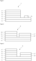
- the emitting device 1 has a stacked structure having a substrate 11, an n-type contact layer 12 (which may be referred to as an n-type nitride semiconductor layer or an electron-transporting layer), an emitting layer 13 (which may be referred to as an active layer), a p-type semiconductor layer 15, an intermediate layer 16, and a reflective electrode layer 17 in this order.
- An electrode layer 18 is formed on a part of the n-type contact layer on which the emitting layer 13 is not formed.
- a dielectric multilayer film using an insulator may be used as the reflective electrode layer to ensure high reflectance.
- the intermediate layer injects electrons and serves as a diffusion layer for electrons.
- Figure 2 is a diagram for explaining another example of the layer configuration of the emitting device according to this aspect.
- the emitting device 2 has a stacked structure (emitting portion) having a substrate 11, an n-type contact layer 12, an emitting layer 13, a p-type semiconductor layer 21, and an electrode layer 22 in this order. Further, the intermediate layer 16' and the reflective electrode layer 17' are provided in this order on a part of the n-type contact layer 12 on which the emitting layer 13 is not formed (electrode portion).
- a high reflectance may be ensured by using a dielectric multilayer film using an insulator as the reflective electrode layer.
- holes are injected from the electrode layer 22 and electrons are injected from the reflective electrode layer 17', respectively, and holes and electrons are recombined in the emitting layer 13 to emit light.
- Part of the light generated in the emitting layer 13 is multiple-reflected by the interface of each layer and the substrate, and enters the electrode portion.
- the light entering the electrode portion is reflected by the reflective electrode layer 17' and can be extracted from the substrate 11, so that the light extraction efficiency can be increased.
- Figure 3 is a diagram for explaining another example of the layer configuration of the emitting device according to this aspect.
- the emitting device 3 has a stacked structure (emitting portion) having a substrate 11, an n-type contact layer 12, an emitting layer 13, a p-type semiconductor layer 15, an intermediate layer 16, and a reflective electrode layer 17 in this order. Further, the intermediate layer 16' and the reflective electrode layer 17' are provided in this order on a part of the n-type contact layer 12 on which the emitting layer 13 is not formed (electrode portion).
- the stacked structure of the p-type semiconductor layer 15, the intermediate layer 16, and the reflective electrode layer 17 and the stacked structure of the n-type contact layer 12, the intermediate layer 16', and the reflective electrode layer 17' correspond to the stacked body according to the present invention described above.
- the emitting device of this aspect has two sets of stacked bodies.
- the emitting device 3 has a structure in which the emitting device 1 and the emitting device 2 are combined.
- holes are injected from the reflective electrode layer 17 and electrons are injected from the reflective electrode layer 17' and holes and electrons are recombined in the emitting layer 13 to emit light.
- the light generated in the emitting layer 13 the light generated in the direction of the reflective electrode layer 17 is reflected by the reflective electrode layer 17 and is extracted from the substrate 11.
- a part of the light generated in the emitting layer 13 is multiple-reflected by the interface of each layer and the substrate and enters the electrode portion, and in this aspect, the light entered the electrode portion is reflected by the reflective electrode layer 17' and is extracted from the substrate 11.
- Figure 4 is a diagram for explaining another example of the layer configuration of the emitting device according to this aspect.
- the emitting device 4 has the same configuration as the emitting device 1 except that the n-type semiconductor layer 25 is provided between the p-type semiconductor layer 15 and the intermediate layer 16.
- the n-type semiconductor layer 25, the intermediate layer 16, and the reflective electrode layer 17 correspond to the stacked body according to the present invention described above.
- a p-type semiconductor layer 15 is provided between the emitting layer 13 and the reflective electrode layer 17, and the p-type semiconductor layer 15 and the n-type semiconductor layer 25 of the stacked body form a tunnel junction structure. This increases the hole injection efficiency into the emitting layer.
- a tunnel junction structure can be formed in the same manner.
- the n-type semiconductor layer 47, the intermediate layer 48, and the reflective electrode layer 49 correspond to the stacked body according to the present invention.
- the n-type contact layer 43 is n-type doped.
- the dopant used for n-type doping is preferably Si when Al composition is 60% or more, and is preferably Ge when Al composition is 60% or less.
- the concentration of the dopant in the n-type contact layer 43 is 8 ⁇ 10 18 cm -3 to 4 ⁇ 10 19 cm -3 , for example.
- the thickness of the n-type contact layer 43 is not particularly limited, and is, for example, 500 nm or more, 700 nm or more, or 900 nm or more, and 4000 nm or less, 3000 nm or less, or 2000 nm or less.
- each of the well layers is, for example, 1 to 6 nm
- the thickness of each of the barrier layers is, for example, 3 to 15 nm.
- the electron-blocking layer 45 have an AlGaN composition.
- the AlGaN composition is not particularly limited, and may be, for example, Al c Ga 1-c N (c is 0.6 or more, 0.65 or more, or 0.7 or more, and is 0.95 or less, 0.9 or less, or 0.8 or less).
- the electron-blocking layer 45 is doped with Mg.
- Mg concentration is, for example, 1 ⁇ 10 18 cm -3 to 2 ⁇ 10 20 cm -3 .
- the thickness of the electron-blocking layer 45 is not particularly limited, and is, for example, 1 nm or more, 2 nm or more, or 5 nm or more, and 40 nm or less, 30 nm or less, or 25 nm or less.
- the p-type semiconductor layer 46 is a hole-transporting layer.
- the p-type semiconductor layer 46 has a first p-type semiconductor layer and a second p-type semiconductor layer in this order on the electron-blocking layer 4.
- the first p-type semiconductor layer has an AlGaN composition.
- the AlGaN composition needs to be changed in Al composition depending on the emitting wavelength in order to suppress light absorption. Incidentally, the higher the Al composition, the lower the carrier concentration and the more the hole injection will be inhibited, so that Al composition is preferable as low as possible.
- the AlGaN composition may be Al d Ga 1-d N (d is 0.3 to 0.8, may be 0.4 to 0.7, and is preferably 0.5 to 0.65).
- the first p-type semiconductor layer is p-type doped.
- Examples of the dopant used for p-type doping include Mg, Zn, Be, and the like.
- the concentration of the dopant in the first p-type semiconductor layer is, for example, 1 ⁇ 10 19 to 1 ⁇ 10 20 cm -3 .
- the second p-type semiconductor layer has an AlGaN composition.
- the AlGaN composition is preferably higher in the Al composition, as in the first p-type semiconductor layer.
- the Al composition is preferable as low as possible.
- the AlGaN composition may be Al e Ga 1-e N (e is 0.3 to 0.8 or 0.4 to 0.7, and is preferably 0.5 to 0.65).
- the thickness of the second p-type semiconductor layer is not particularly limited, and is, for example, 1 nm or more, 2 nm or more, or 5 nm or more, and 200 nm or less, 150 nm or less, or 100 nm or less.
- the first n-type semiconductor layer has an AlGaN composition.
- Al composition is preferably as high as possible from the viewpoint of light extraction.
- it is preferable that Al composition is as low as possible from the viewpoint of the carrier tunneling probabilities.
- the AlGaN composition may be Al f Ga 1-f N (f is 0.3 to 0.8 or 0.4 to 0.7, and is preferably 0.5 to 0.65).
- the thickness of the first n-type semiconductor layer is not particularly limited, and is, for example, 1 nm or more, 2 nm or more, or 5 nm or more, and 200 nm or less, 100 nm or less, or 50 nm or less.
- the second n-type semiconductor layer has an AlGaN composition.
- Al composition is preferably as high as possible from the viewpoint of light extraction.
- it is preferable that Al composition is as low as possible from the viewpoint of the carrier tunneling probabilities.
- the AlGaN composition may be Al g Ga 1-g N (g is 0.3 to 0.8 or 0.4 to 0.7, and is preferably 0.5 to 0.65).
- the method of forming the buffer layer 42, the n-type contact layer 43, the emitting layer 44, the electron-blocking layer 45, the p-type semiconductor layer 46, and the n-type semiconductor layer 47 is not particularly limited, and metalorganic vapor phase epitaxy (MOVPE) method and the like can be used.
- MOVPE metalorganic vapor phase epitaxy
- the reflective electrode layer 49 is an anode and is configured to reflect light from the intermediate layer 48 side to the intermediate layer 48 side.
- the light from the intermediate layer 48 side may be light including deep ultraviolet rays emitted in the emitting layer 44.
- the description of the reflective electrode layer 49 is the same as the description of the reflective electrode layer of the stacked body described above.
- the auxiliary electrode layer 51 is formed on the reflective electrode layer 49.
- the auxiliary electrode layer 51 may be made of a conductive material.
- the conductive material include a metal and the like.
- the metal include one metal or an alloy of two or more metals selected from the group consisting of V, Al, Ti, Pt, and Au.
- V vanadium
- Ti titanium
- Pt palladium
- Au gold
- the thickness of the auxiliary electrode layer 51 is not particularly limited, and is, for example, 0.5 to 10 nm, and is preferably 1 to 5 nm.
- the electrode layer 52 may be formed of a conductive material.
- the conductive material include a metal and the like.
- the metal include one metal or an alloy of two or more metals selected from the group consisting of V, Al, Ti, Pt, Au, In, and Sn.
- the thickness (total thickness) of the electrode layer 52 is not particularly limited, and is desirably, for example, 100 to 1000 nm, and preferably 100 to 500 nm.
- the n-type semiconductor layer and the p-type semiconductor layer are tunnel junctioned.
- the emitting device has an emitting wavelength in the deep ultraviolet range. Specifically, the emitting device has an emitting wavelength in the range of 200 to 350 nm, preferably in the range of 210 to 310 nm, more preferably in the range of 220 to 290 nm.
- An emitting device having a layer configuration similar to that of Figure 5 was produced by the following method.
- a buffer layer 42, an n-type contact layer 43, an emitting layer 44, an electron-blocking layer 45, a p-type semiconductor layer 46, and an n-type semiconductor layer 47 were deposited in this order on a c-plane (0001) of a sapphire substrate (thickness: 200 ⁇ m) as the substrate 41 by a metalorganic vapor phase epitaxy (MOVPE) method.
- MOVPE metalorganic vapor phase epitaxy
- an n-type contact layer 43 made of an AlGaN containing Si was formed on the buffer layer 42 by MOVPE method.
- the growth conditions for the n-type contact layer 43 are 980°C for the growth temperature and 50 to 150 mbar for the growth pressure.
Landscapes
- Led Devices (AREA)
Applications Claiming Priority (2)
| Application Number | Priority Date | Filing Date | Title |
|---|---|---|---|
| JP2021136988 | 2021-08-25 | ||
| PCT/JP2022/031704 WO2023027064A1 (ja) | 2021-08-25 | 2022-08-23 | 発光素子用の反射電極 |
Publications (2)
| Publication Number | Publication Date |
|---|---|
| EP4394902A1 true EP4394902A1 (de) | 2024-07-03 |
| EP4394902A4 EP4394902A4 (de) | 2025-10-01 |
Family
ID=85322821
Family Applications (1)
| Application Number | Title | Priority Date | Filing Date |
|---|---|---|---|
| EP22861352.7A Pending EP4394902A4 (de) | 2021-08-25 | 2022-08-23 | Reflektierende elektrode für ein lichtemittierendes element |
Country Status (6)
| Country | Link |
|---|---|
| US (1) | US20250241093A1 (de) |
| EP (1) | EP4394902A4 (de) |
| KR (1) | KR20240046512A (de) |
| CN (1) | CN117813695A (de) |
| TW (1) | TW202318685A (de) |
| WO (1) | WO2023027064A1 (de) |
Family Cites Families (8)
| Publication number | Priority date | Publication date | Assignee | Title |
|---|---|---|---|---|
| JP4431925B2 (ja) * | 2000-11-30 | 2010-03-17 | 信越半導体株式会社 | 発光素子の製造方法 |
| KR100896564B1 (ko) * | 2004-08-31 | 2009-05-07 | 삼성전기주식회사 | 반사전극 및 이를 구비하는 화합물 반도체 발광소자 |
| JP2011060917A (ja) * | 2009-09-08 | 2011-03-24 | Rohm Co Ltd | 半導体発光素子 |
| JP2013120829A (ja) | 2011-12-07 | 2013-06-17 | Sharp Corp | 窒化物半導体紫外発光素子 |
| JP6771065B2 (ja) * | 2014-01-20 | 2020-10-21 | ローム株式会社 | 発光素子および発光素子パッケージ |
| JP6727185B2 (ja) * | 2017-12-28 | 2020-07-22 | 日機装株式会社 | 窒化物半導体発光素子 |
| KR102573271B1 (ko) * | 2018-04-27 | 2023-08-31 | 삼성전자주식회사 | 반도체 발광소자 |
| US12439742B2 (en) * | 2018-09-26 | 2025-10-07 | Idemitsu Kosan Co., Ltd. | Light emitting device with electrode having specified molar ratio of magnesium to zinc |
-
2022
- 2022-08-23 CN CN202280056342.8A patent/CN117813695A/zh active Pending
- 2022-08-23 KR KR1020247005794A patent/KR20240046512A/ko active Pending
- 2022-08-23 US US18/685,114 patent/US20250241093A1/en active Pending
- 2022-08-23 EP EP22861352.7A patent/EP4394902A4/de active Pending
- 2022-08-23 WO PCT/JP2022/031704 patent/WO2023027064A1/ja not_active Ceased
- 2022-08-25 TW TW111132061A patent/TW202318685A/zh unknown
Also Published As
| Publication number | Publication date |
|---|---|
| TW202318685A (zh) | 2023-05-01 |
| KR20240046512A (ko) | 2024-04-09 |
| US20250241093A1 (en) | 2025-07-24 |
| WO2023027064A1 (ja) | 2023-03-02 |
| JPWO2023027064A1 (de) | 2023-03-02 |
| EP4394902A4 (de) | 2025-10-01 |
| CN117813695A (zh) | 2024-04-02 |
Similar Documents
| Publication | Publication Date | Title |
|---|---|---|
| CN110462851B (zh) | Iii族氮化物半导体发光元件及其制造方法 | |
| EP3331035B1 (de) | Lichtemittierendes gruppe-iii-nitrid-halbleiterbauelement und herstellungsverfahren dafür | |
| CN109980057B (zh) | 第iii族氮化物半导体发光元件和其制造方法 | |
| CN111164768B (zh) | 深紫外发光元件及其制造方法 | |
| US8487344B2 (en) | Optical device and method of fabricating the same | |
| US7910935B2 (en) | Group-III nitride-based light emitting device | |
| JP5244980B2 (ja) | 半導体発光素子 | |
| CN113169255B (zh) | Iii族氮化物半导体发光元件及其制造方法 | |
| US20010001079A1 (en) | Electrode structure and method for fabricating the same | |
| EP3879583B1 (de) | Lichtemittierende iii-nitrid-halbleitervorrichtung und verfahren zu deren herstellung | |
| US7002180B2 (en) | Bonding pad for gallium nitride-based light-emitting device | |
| KR20050051920A (ko) | 플립칩형 질화물계 발광소자 및 그 제조방법 | |
| TWI666790B (zh) | Iii族氮化物半導體發光元件的製造方法及iii族氮化物半導體發光元件 | |
| EP4394902A1 (de) | Reflektierende elektrode für ein lichtemittierendes element | |
| US20100062558A1 (en) | Method for producing transparent conductive layer comprising TIO2 and method for producing semiconductor light-emitting element utilizing said method for producing transparent conductive layer | |
| JP2020129697A (ja) | 深紫外発光素子用の反射電極の製造方法、深紫外発光素子の製造方法および深紫外発光素子 | |
| CN113330586A (zh) | 深紫外发光元件用反射电极的制造方法、深紫外发光元件的制造方法及深紫外发光元件 | |
| US7190076B2 (en) | Electrode for p-type Group III nitride compound semiconductor layer and method for producing the same | |
| JP7413599B1 (ja) | Iii-v族化合物半導体発光素子及びiii-v族化合物半導体発光素子の製造方法 | |
| JP7387048B1 (ja) | 半導体発光素子及び半導体発光素子の製造方法 | |
| WO2025100352A1 (ja) | 紫外発光素子 | |
| JP2001185757A (ja) | Iii族窒化物系化合物半導体発光素子 |
Legal Events
| Date | Code | Title | Description |
|---|---|---|---|
| STAA | Information on the status of an ep patent application or granted ep patent |
Free format text: STATUS: THE INTERNATIONAL PUBLICATION HAS BEEN MADE |
|
| PUAI | Public reference made under article 153(3) epc to a published international application that has entered the european phase |
Free format text: ORIGINAL CODE: 0009012 |
|
| STAA | Information on the status of an ep patent application or granted ep patent |
Free format text: STATUS: REQUEST FOR EXAMINATION WAS MADE |
|
| 17P | Request for examination filed |
Effective date: 20240219 |
|
| AK | Designated contracting states |
Kind code of ref document: A1 Designated state(s): AL AT BE BG CH CY CZ DE DK EE ES FI FR GB GR HR HU IE IS IT LI LT LU LV MC MK MT NL NO PL PT RO RS SE SI SK SM TR |
|
| DAV | Request for validation of the european patent (deleted) | ||
| DAX | Request for extension of the european patent (deleted) | ||
| REG | Reference to a national code |
Ref country code: DE Ref legal event code: R079 Free format text: PREVIOUS MAIN CLASS: H01L0033320000 Ipc: H10H0020825000 |
|
| A4 | Supplementary search report drawn up and despatched |
Effective date: 20250902 |
|
| RIC1 | Information provided on ipc code assigned before grant |
Ipc: H10H 20/825 20250101AFI20250827BHEP Ipc: H10H 20/832 20250101ALI20250827BHEP |