EP4394891A1 - Thin-film transistor array substrate and manufacturing method therefor - Google Patents
Thin-film transistor array substrate and manufacturing method therefor Download PDFInfo
- Publication number
- EP4394891A1 EP4394891A1 EP21794701.9A EP21794701A EP4394891A1 EP 4394891 A1 EP4394891 A1 EP 4394891A1 EP 21794701 A EP21794701 A EP 21794701A EP 4394891 A1 EP4394891 A1 EP 4394891A1
- Authority
- EP
- European Patent Office
- Prior art keywords
- layer
- substrate
- channel portion
- thin
- film transistor
- Prior art date
- Legal status (The legal status is an assumption and is not a legal conclusion. Google has not performed a legal analysis and makes no representation as to the accuracy of the status listed.)
- Pending
Links
Images


Classifications
-
- H—ELECTRICITY
- H10—SEMICONDUCTOR DEVICES; ELECTRIC SOLID-STATE DEVICES NOT OTHERWISE PROVIDED FOR
- H10D—INORGANIC ELECTRIC SEMICONDUCTOR DEVICES
- H10D30/00—Field-effect transistors [FET]
- H10D30/60—Insulated-gate field-effect transistors [IGFET]
- H10D30/67—Thin-film transistors [TFT]
- H10D30/674—Thin-film transistors [TFT] characterised by the active materials
- H10D30/6755—Oxide semiconductors, e.g. zinc oxide, copper aluminium oxide or cadmium stannate
-
- H—ELECTRICITY
- H10—SEMICONDUCTOR DEVICES; ELECTRIC SOLID-STATE DEVICES NOT OTHERWISE PROVIDED FOR
- H10D—INORGANIC ELECTRIC SEMICONDUCTOR DEVICES
- H10D30/00—Field-effect transistors [FET]
- H10D30/01—Manufacture or treatment
- H10D30/021—Manufacture or treatment of FETs having insulated gates [IGFET]
- H10D30/031—Manufacture or treatment of FETs having insulated gates [IGFET] of thin-film transistors [TFT]
-
- H—ELECTRICITY
- H10—SEMICONDUCTOR DEVICES; ELECTRIC SOLID-STATE DEVICES NOT OTHERWISE PROVIDED FOR
- H10D—INORGANIC ELECTRIC SEMICONDUCTOR DEVICES
- H10D30/00—Field-effect transistors [FET]
- H10D30/60—Insulated-gate field-effect transistors [IGFET]
- H10D30/67—Thin-film transistors [TFT]
- H10D30/6704—Thin-film transistors [TFT] having supplementary regions or layers in the thin films or in the insulated bulk substrates for controlling properties of the device
- H10D30/6713—Thin-film transistors [TFT] having supplementary regions or layers in the thin films or in the insulated bulk substrates for controlling properties of the device characterised by the properties of the source or drain regions, e.g. compositions or sectional shapes
-
- H—ELECTRICITY
- H10—SEMICONDUCTOR DEVICES; ELECTRIC SOLID-STATE DEVICES NOT OTHERWISE PROVIDED FOR
- H10D—INORGANIC ELECTRIC SEMICONDUCTOR DEVICES
- H10D30/00—Field-effect transistors [FET]
- H10D30/60—Insulated-gate field-effect transistors [IGFET]
- H10D30/67—Thin-film transistors [TFT]
- H10D30/6704—Thin-film transistors [TFT] having supplementary regions or layers in the thin films or in the insulated bulk substrates for controlling properties of the device
- H10D30/6713—Thin-film transistors [TFT] having supplementary regions or layers in the thin films or in the insulated bulk substrates for controlling properties of the device characterised by the properties of the source or drain regions, e.g. compositions or sectional shapes
- H10D30/6715—Thin-film transistors [TFT] having supplementary regions or layers in the thin films or in the insulated bulk substrates for controlling properties of the device characterised by the properties of the source or drain regions, e.g. compositions or sectional shapes characterised by the doping profiles, e.g. having lightly-doped source or drain extensions
-
- H—ELECTRICITY
- H10—SEMICONDUCTOR DEVICES; ELECTRIC SOLID-STATE DEVICES NOT OTHERWISE PROVIDED FOR
- H10D—INORGANIC ELECTRIC SEMICONDUCTOR DEVICES
- H10D30/00—Field-effect transistors [FET]
- H10D30/60—Insulated-gate field-effect transistors [IGFET]
- H10D30/67—Thin-film transistors [TFT]
- H10D30/6729—Thin-film transistors [TFT] characterised by the electrodes
- H10D30/673—Thin-film transistors [TFT] characterised by the electrodes characterised by the shapes, relative sizes or dispositions of the gate electrodes
-
- H—ELECTRICITY
- H10—SEMICONDUCTOR DEVICES; ELECTRIC SOLID-STATE DEVICES NOT OTHERWISE PROVIDED FOR
- H10D—INORGANIC ELECTRIC SEMICONDUCTOR DEVICES
- H10D30/00—Field-effect transistors [FET]
- H10D30/60—Insulated-gate field-effect transistors [IGFET]
- H10D30/67—Thin-film transistors [TFT]
- H10D30/6757—Thin-film transistors [TFT] characterised by the structure of the channel, e.g. transverse or longitudinal shape or doping profile
-
- H—ELECTRICITY
- H10—SEMICONDUCTOR DEVICES; ELECTRIC SOLID-STATE DEVICES NOT OTHERWISE PROVIDED FOR
- H10D—INORGANIC ELECTRIC SEMICONDUCTOR DEVICES
- H10D30/00—Field-effect transistors [FET]
- H10D30/60—Insulated-gate field-effect transistors [IGFET]
- H10D30/67—Thin-film transistors [TFT]
- H10D30/6758—Thin-film transistors [TFT] characterised by the insulating substrates
-
- H—ELECTRICITY
- H10—SEMICONDUCTOR DEVICES; ELECTRIC SOLID-STATE DEVICES NOT OTHERWISE PROVIDED FOR
- H10D—INORGANIC ELECTRIC SEMICONDUCTOR DEVICES
- H10D99/00—Subject matter not provided for in other groups of this subclass
Definitions
- the method further comprises: depositing a buffer layer on the substrate to cover the platform layer, and the buffer layer is formed by a photolithography process to form a convex portion located directly above the platform layer, wherein the channel portion is disposed on the convex portion and covers the entire convex portion.
- Step S70 depositing an interlayer dielectric layer to cover the oxide active layer, the gate insulating layer, and the gate electrode, and patterning the interlayer dielectric layer to form a plurality of via holes.
- an interlayer dielectric layer 16 is made of a material, such as silicon oxide or silicon nitride, of is configured with a multilayer structure film, and has a thickness between 1000 ⁇ and 8000 ⁇ .
- the interlayer dielectric layer 16 after being patterned exposes source/drain electrode contact regions in the oxide active layer 13 and forms a plurality of via holes 160.
Landscapes
- Thin Film Transistor (AREA)
Abstract
Description
- The present invention relates to a technical field of displays, and more particularly to a thin-film transistor array substrate and a method of manufacturing the same.
- With development of display technologies, flat panel displays have become mainstream displays at present. General flat panel displays include liquid crystal displays (LCDs) and active matrix organic light-emitting diodes (AMOLEDs).
- In the flat panel displays, thin-film transistor (TFT) array substrates are main driving elements and necessary structures for high-performance flat panel display devices. The TFT array substrates include a plurality of thin-film transistors arranged in an array. There are different types of thin-film transistors, such as bottom gate thin-film transistors or top gate thin-film transistors. The top gate thin-film transistors have lower parasitic capacitance and better ductility because there is no overlap between source/drain electrodes and gate electrodes, and can reduce delays in signal transmission. In technologies of metal oxide thin-film transistors with top gate structures, in order to reduce resistance occurred outside channels, self-aligned etching processes are often used. That is, gate patterns are formed at a same time when gate insulating layers are etched through one time of photolithography process, which is also used for non-channel portions in electrically conductive formation, so that it can effectively prevent high resistance regions on both sides of the channel from being caused by alignment deviation However, diffusion of conductive effects on both ends of the channel will lead to low-resistance regions at the both ends of the channel. That is, an effective channel length becomes shorter, which is not conducive to downsizing of TFT devices.
- An object of the present application is to provide a thin-film transistor array substrate and a method of manufacturing the same to overcome a technical problem that diffusion of electrically conductive effects on both ends of a channel of a conventional thin-film transistor device will lead to low-resistance regions at the both ends of the channel, resulting in a decrease in an effective channel length, which is not conducive to downsizing of thin-film transistor devices.
- To achieve the above-mentioned object, the present application provides a technical solution as follows:
- An embodiment of the present application provides a thin-film transistor array substrate, comprising a substrate; a platform layer disposed on the substrate; an oxide active layer disposed on the substrate and located above the platform layer and comprising a channel portion and conductor portions located on opposite sides of the channel portion, wherein a vertical level of a top surface of the channel portion is higher than a vertical level of a top surface of any one of the conductor portions; a gate insulating layer disposed on the oxide active layer; a gate electrode disposed on the gate insulating layer, wherein an orthographic projection of the gate electrode on the substrate covers orthographic projections of the platform layer and the channel portion on the substrate; and a source electrode and a drain electrode both electrically connected to the conductor portions.
- Further, the thin-film transistor array substrate further comprises a buffer layer disposed on the substrate and covers the platform layer, wherein the platform layer is made of an insulating material or a metal oxide.
- Further, the buffer layer comprises a convex portion, and the channel portion is disposed on the convex portion and covers the entire convex portion.
- Further, the channel portion comprises two slopes, and one end of each of the slopes is connected to a corresponding one of the conductor portions, wherein each of the slopes is inclined in a direction away from the channel portion and toward the corresponding conductor portion.
- Further, the platform layer comprises a first end surface and a second end surface inclined outward, respectively, and the orthographic projection of the channel portion on the substrate covers the orthographic projection of the platform layer on the substrate.
- Further, the gate insulating layer comprises two offset portions disposed opposite to each other, wherein each of the offset portions is defined between a side edge of the gate electrode and a side edge of the gate insulating layer adjacent to the side edge of the gate electrode such that orthographic projections of the two offset portions on the substrate cover orthographic projections of the first end surface and the second end surface of the platform layer and orthographic projections of the slopes of the channel portion on the substrate, respectively.
- Further, the thin-film transistor array substrate further comprises an interlayer dielectric layer covering the oxide active layer, the gate insulating layer, and the gate electrode, and comprising a plurality of via holes, wherein the source electrode and the drain electrode are arranged on the interlayer dielectric layer and are electrically connected to the conductor portions through the via holes.
- An embodiment of the present application further provides a method of manufacturing a thin-film transistor array substrate, comprising depositing a platform layer on a substrate, wherein the platform layer is made of an insulating material or a metal oxide; forming an oxide active layer on the substrate, and forming a channel portion and conductor regions located on two opposite sides of the channel portion by using a photolithography process; depositing a gate insulating layer on the oxide active layer; depositing a gate metal layer on the gate insulating layer; forming, by using a photolithography process to pattern the gate metal layer, a gate electrode, and etching self-alignedly the gate insulating layer to expose the conductor portions of the oxide active layer, wherein an orthographic projection of the gate electrode on the substrate covers orthographic projections of the platform layer and the channel portion on the substrate; performing a plasma treatment in a full-surface way to make the conductor regions of the oxide active layer conductive to form conductor portions, wherein a vertical level of a top surface of the channel portion is higher than a vertical level of a top surface of any one of the conductor portions; depositing an interlayer dielectric layer to cover the oxide active layer, the gate insulating layer, and the gate electrode, and patterning the interlayer dielectric layer to form a plurality of via holes; and depositing and patterning a source electrode/drain electrode metal layer into a source electrode and a drain electrode, wherein the source electrode and the drain electrode are electrically connected to the conductor portions of the oxide active layer through the via holes.
- Further, prior to the step of forming the oxide active layer on the substrate, the method further comprises: depositing a buffer layer on the substrate to cover the platform layer, and the buffer layer is formed by a photolithography process to form a convex portion located directly above the platform layer, wherein the channel portion is disposed on the convex portion and covers the entire convex portion.
- Further, the channel portion comprises two slopes, one end of each of the slopes is connected to a corresponding one of the conductor portions, and each of the slopes is inclined in a direction away from the channel portion and toward the corresponding conductor portion, wherein the gate insulating layer comprises two offset portions disposed opposite to each other, wherein each of the offset portions is formed between a side edge of the gate electrode and a side edge of the gate insulating layer adjacent to the side edge of the gate electrode such that orthographic projections of the two offset portions on the substrate cover orthographic projections of the first end surface and the second end surface of the platform layer and orthographic projections of the slopes of the channel portion on the substrate, respectively.
- An embodiment of the present application further provides a thin-film transistor array substrate, comprising a substrate; a platform layer disposed on the substrate, wherein the platform layer is made of an insulating material or a metal oxide; an oxide active layer disposed on the substrate and located above the platform layer, and comprising a channel portion and conductor portions located on opposite sides of the channel portion, wherein the channel portion comprises two slopes, one end of each of the slopes is connected to a corresponding one of the conductor portions, and the other end extends from the channel portion, wherein a vertical level of a top surface of the channel portion is higher than a vertical level of a top surface of any one of the conductor portions; a gate insulating layer disposed on the oxide active layer; a gate electrode disposed on the gate insulating layer, wherein an orthographic projection of the gate electrode on the substrate covers orthographic projections of the platform layer and the channel portion on the substrate; and a source electrode and a drain electrode both electrically connected to the conductor portions.
- The present application has advantageous effects as follows: embodiments of the present application provide a thin-film transistor array substrate and a method of manufacturing the same. A platform layer and adjustment of angles of a first end surface and a second end surface of the platform layer are used to allow for formation of gentle slope-shaped offset portions of upper film layer structures, such that orthographic projections of the offset portions on a substrate cover orthographic projections of slopes of a channel portion on the substrate, and fall on a first end surface and a second end surface of the platform layer, respectively. With the provision of the offset portions, a conductive diffusion path of the oxide active layer is extended such that lengths of low-resistance regions formed through diffusion from two ends of the channel portion to an inside of the channel portion are reduced after the self-aligned etching process, so as to effectively regulate or suppress shortening of an effective channel length, and ensure the effective channel length, thereby facilitating fulfillment of downsizing of thin-film transistor devices and effectively overcoming a technical problem that diffusion of electrically conductive effects on both ends of a channel of a conventional thin-film transistor device will lead to low-resistance regions at the both ends of the channel, resulting in a decrease in an effective channel length, which is not conducive to downsizing of thin-film transistor devices.
- To describe the technical solutions in the embodiments of the present invention, the following briefly introduces the accompanying drawings for describing the embodiments. Apparently, the accompanying drawings in the following description show merely some embodiments of the present invention, and a person skilled in the art may still derive other drawings from these accompanying drawings without creative efforts.
-
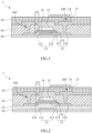
FIG. 1 is a schematic cross-sectional plan view of a thin-film transistor array substrate of an embodiment of the present application. -
FIG. 2 is a schematic cross-sectional view of a thin-film transistor array substrate of another embodiment of the present application. -
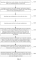
FIG. 3 is a flowchart of a method of manufacturing a thin-film transistor array substrate of an embodiment of the present application. -
FIGs. 4 to 11 are schematic views of film layer structures of a thin-film transistor fabricated in each step in the method of manufacturing the thin-film transistor array substrate according to the embodiment of the application. - The following embodiments are referring to the accompanying drawings for exemplifying specific implementable embodiments of the present invention. Directional terms described by the present invention, such as upper, lower, front, back, left, right, inner, outer, side, etc., are only directions by referring to the accompanying drawings, and thus the used directional terms are used to describe and understand the present invention, but the present invention is not limited thereto. In the drawings, units with similar structures are indicated by the same reference numerals. In the drawings, for clear understanding and ease of description, the thickness of some layers and regions are exaggerated. That is, the size and thickness of each component shown in the drawings are arbitrarily shown, but the application is not limited to them.
- An embodiment of the present application provides a thin-film transistor, which can be arranged in an array and fabricated into a thin-film transistor array substrate. The thin-film transistor array substrate is provided with a plurality of gate scan lines and a plurality of data lines. The gate scan lines and the data lines collectively define a plurality of pixel units, and each of the pixel units is provided with the thin-film transistor and a pixel electrode. The thin-film transistor array substrate may serve as a driving substrate of a liquid crystal display or an organic light-emitting diode display.
- Please refer to
FIG. 1 , which is a schematic cross-sectional plan view of a thin-filmtransistor array substrate 1 of an embodiment of the present application. As shown inFIG. 1 , the thin-filmtransistor array substrate 1 provided by the embodiment of the present application includes asubstrate 10, aplatform layer 11, an oxideactive layer 13, agate insulating layer 14, agate electrode 15, an interlayerdielectric layer 16, source anddrain electrodes 17, apassivation layer 18, and apixel electrode 19 arranged in sequence. A material of thesubstrate 10 can be glass or transparent plastic and other materials, preferably glass. Theplatform layer 11 is disposed on a surface of thesubstrate 10. Specifically, an insulating material is used to deposit a layer of platform film, which is being patterned through a photolithography process to form theplatform layer 11. Theplatform layer 11 includes a top surface, afirst end surface 111, and asecond end surface 112. It should be noted that thefirst end surface 111 and thesecond end surface 112 are disposed at two opposite ends of theplatform layer 11, respectively. Each of thefirst end surface 111 and thesecond end surface 112 tilts outward in a direction from the top surface of theplatform layer 11 toward thesubstrate 10. Preferably, thefirst end surface 111 and thesubstrate 10 form an angle between 40° and 80°, and thesecond end surface 112 forms an angle between 40° and 80° with respect to thesubstrate 10. In one embodiment, the angle between thefirst end surface 111 and thesubstrate 10 is the same as the angle between thesecond end surface 112 and thesubstrate 10. It should be noted that the above-mentioned angle range is set according to capability ranges of etching processes, and can facilitate oblique formation of upper film layers. - As shown in
FIG. 1 , the oxideactive layer 13 is disposed on thesubstrate 10. The oxideactive layer 13 can be a metal oxide semiconductor made of a material, such as indium gallium zinc oxide (IGZO), indium zinc tin oxide (IZTO) or indium gallium zinc tin oxide (IGZTO). The oxideactive layer 13 includes achannel portion 131 andconductor portions 132 located on opposite sides of thechannel portion 131, wherein thechannel portion 131 is located directly above theplatform layer 11. It should be noted that since theplatform layer 11 is disposed on the surface of thesubstrate 10, a height of thechannel portion 131 is thus raised, so that thechannel portion 131 and theconductor portion 132 are located at different horizontal positions, respectively. That is, a vertical level of a top surface of thechannel portion 131 is higher than a vertical level of a top surface of any one of theconductor portions 132. Specifically, thechannel portion 131 includes twoslopes 133, and one end of each of theslopes 133 is connected to a corresponding one of theconductor portions 132, the other end extends from thechannel portion 131. Each of theslopes 133 is inclined in a direction away from thechannel portion 131 and toward the correspondingconductor portion 132. - Continuing referring to
FIG. 1 , thegate insulating layer 14 is disposed on the oxideactive layer 13. Thegate electrode 15 is disposed on thegate insulating layer 14. It should be noted that thegate electrode 15 is formed by patterning a gate metal layer through a photolithography process, and thegate insulating layer 14 is being etched self-alignedly to exposeconductor regions 130 of the oxideactive layer 13. Then, a plasma treatment is performed in a way of full-surface to make theconductor regions 130 of the oxideactive layer 13 conductive, thereby formingconductor portions 132. Specifically, after thegate insulating layer 14 undergoes the photolithography process and self-aligned etching, two offsetportions 141 are formed. The two offsetportions 141 are disposed at two opposite ends of thegate insulating layer 14, and each of the offsetportions 141 is arranged in conformity with a corresponding one of theslopes 133 of thechannel portion 131 and covers thecorresponding slope 133. Specifically, each of the offsetportions 141 is defined between a side edge of thegate electrode 15 and a side edge of thegate insulating layer 14 adjacent to the side edge of thegate electrode 15. It should be noted that a length of theplatform layer 11 is less than a length of thechannel portion 131 and is substantially the same as a length of thegate electrode 15. That is, an orthographic projection of thegate electrode 15 on thesubstrate 10 covers orthographic projections of theplatform layer 11 and thechannel portion 131 on thesubstrate 10. In this embodiment, a length difference between theplatform layer 11 and thegate electrode 15 is less than two microns. It can be seen from the schematic cross-sectional view of the thin-filmtransistor array substrate 1 inFIG. 1 that thefirst end surface 111 and thesecond end surface 112 of theplatform layer 11 each extend beyond a length range of thegate electrode 15 in vertical cross-section. In other words, an orthographic projection of each offsetportion 141 on thesubstrate 10 covers an orthographic projection of thefirst end surface 111 or an orthographic projection of thesecond end surface 112 of theplatform layer 11 on thesubstrate 10. - As shown in
FIG. 1 , aninterlayer dielectric layer 16 is deposited on thesubstrate 10 to cover the oxideactive layer 13, thegate insulating layer 14, and thegate electrode 15. Theinterlayer dielectric layer 16 is patterned to form a plurality of viaholes 160. The source electrode and thedrain electrode 17 are disposed on theinterlayer dielectric layer 16 and are electrically connected to theconductor portions 132 of the oxideactive layer 13 through corresponding viaholes 160. In addition, apassivation layer 18 is further formed on theinterlayer dielectric layer 16 and is made of a material, such as nitride (silicon nitride, etc.) or oxide (silicon oxide, silicon dioxide), or is configured with a multilayer structure film. In another embodiment, a planarization layer (not shown) is further disposed on thepassivation layer 18. The planarization layer can provide further protection for underlying film layers and provide a better planarization effect. Apixel electrode 19 is disposed on thepassivation layer 18 or on the planarization layer. Thepixel electrode 19 is formed through a patterned metal layer and is electrically connected to the source electrode and thedrain electrode 17 through a throughhole 180. Based on the aforementioned components, the embodiment of the present application provides a top gate thin-filmtransistor array substrate 1, which can serve as a driving substrate for subsequent liquid crystal displays or organic light-emitting diode displays. - Please refer to
FIG. 2 , which is a schematic cross-sectional view of the thin-filmtransistor array substrate 1 in another embodiment of the present application. A difference between the embodiments shown inFIG. 2 and FIG. 1 is that the thin-filmtransistor array substrate 1 ofFIG. 2 is further provided with a buffer layer 12 (details will be described later). Other same components in the aforementioned embodiments will not be described in detail here. As shown inFIG. 2 , the thin-filmtransistor array substrate 1 provided by the embodiment of the application includes asubstrate 10, aplatform layer 11, abuffer layer 12, an oxideactive layer 13, agate insulating layer 14, agate electrode 15, aninterlayer dielectric layer 16, and source and drainelectrodes 17, apassivation layer 18, and apixel electrode 19. Specifically, an insulating material or a metal oxide material is used to deposit a layer of platform film, which is being patterned through a photolithography process to form theplatform layer 11 . - Continuing referring to
FIG. 2 , abuffer layer 12 is deposited on thesubstrate 10 to cover theplatform layer 11. Specifically, thebuffer layer 12 is made of a material, such as nitride (silicon nitride, etc.) or oxide (silicon oxide, silicon dioxide), or is configured with a multilayer structure film. Thebuffer layer 12 formed by deposition has aconvex portion 121 located corresponding to the underlying platform layer. It should be noted that in the embodiment shown inFIG. 1 , theplatform layer 11 is made of an insulating material, so thebuffer layer 12 may not be provided. But, in order to improve adhesion between the glass substrate and functional layers on a surface of the glass substrate, and to fulfill a function of preventing impurities inside the glass substrate from diffusing into each functional layer during a process, the thin-filmtransistor array substrate 1 of the embodiment of the present application is provided with thebuffer layer 12 disposed on another embodiment, in order to improve adhesion between the glass substrate and functional layers on a surface of the glass substrate, and to fulfill a function of preventing impurities inside the glass substrate from diffusing into each function layer during a process, the thin-filmtransistor array substrate 1 of the embodiment of the present application is provided with thebuffer layer 12 disposed on thesubstrate 10 on thesubstrate 10 - As shown in
FIG. 2 , an oxideactive layer 13 is deposited on thebuffer layer 12. The oxideactive layer 13 includes achannel portion 131 andconductor portions 132 located on opposite sides of thechannel portion 131. It should be noted that thechannel portion 131 and theconductor portions 132 are located at different horizontal positions, that is, a vertical level of a top surface of thechannel portion 131 is higher than a vertical level of a top surface of any one of theconductor portions 132. Specifically, thechannel portion 131 is disposed on theconvex portion 121 of thebuffer layer 12 and covers the entireconvex portion 121. It should be noted that thechannel portion 131 includes twoslopes 133, and one end of each of theslopes 133 is connected to a corresponding one of theconductor portions 132, the other end extends from thechannel portion 131. Each of theslopes 133 is inclined in a direction away from thechannel portion 131 and toward the correspondingconductor portion 132. As shown inFIG. 2 , thebuffer layer 12 is disposed between the oxideactive layer 13 and thesubstrate 10 and theplatform layer 11. - Continuing referring to
FIG. 2 , thegate insulating layer 14 is disposed on the oxideactive layer 13. Thegate electrode 15 is disposed on thegate insulating layer 14. Furthermore, after thegate insulating layer 14 undergoes the photolithography process and self-aligned etching, two offsetportions 141 are formed. The two offsetportions 141 are disposed at two opposite ends of thegate insulating layer 14, and each of the offsetportions 141 is arranged in conformity with a corresponding one of theslopes 133 of thechannel portion 131 and covers thecorresponding slope 133. Specifically, each of the offsetportions 141 is defined between a side edge of thegate electrode 15 and a side edge of thegate insulating layer 14 adjacent to the side edge of thegate electrode 15. It should be noted that a length of theplatform layer 11 is less than a length of thechannel portion 131 and is substantially the same as a length of thegate electrode 15. That is, an orthographic projection of thechannel portion 131 on thesubstrate 10 covers an orthographic projection of theplatform layer 11 on thesubstrate 10. In addition, an orthographic projection of thegate electrode 15 on thesubstrate 10 covers the orthographic projections of theplatform layer 11 and thechannel portion 131 on thesubstrate 10. In this embodiment, a length difference between theplatform layer 11 and thegate electrode 15 is less than two microns. It can be seen from the schematic cross-sectional view of the thin-filmtransistor array substrate 1 inFIG. 2 that afirst end surface 111 and asecond end surface 112 of theplatform layer 11 are inclined at between 40° and 80° to the horizontal, so that thefirst end surface 111 and thesecond end surface 112 each extend beyond a length range of thegate electrode 15 in vertical cross-section. In other words, an orthographic projection of each offsetportion 141 on thesubstrate 10 falls on thefirst end surface 111 or thesecond end surface 112 of theplatform layer 11. - As shown in
FIG. 2 , theinterlayer dielectric layer 16 is deposited on thebuffer layer 12 to cover the oxideactive layer 13, thegate insulating layer 14, and thegate electrode 15, and theinterlayer dielectric layer 16 is patterned to form a plurality of viaholes 160. The source electrode and thedrain electrode 17 are disposed on theinterlayer dielectric layer 16 and are electrically connected to theconductor portions 132 of the oxideactive layer 13 through corresponding viaholes 160. In addition, apassivation layer 18 is further formed on theinterlayer dielectric layer 16. In another embodiment, a planarization layer (not shown) is further provided on thepassivation layer 18. Apixel electrode 19 is formed on thepassivation layer 18 or on the planarization layer. Thepixel electrode 19 is electrically connected to the source electrode and thedrain electrode 17 through a throughhole 180. Based on the aforementioned components, the embodiment of the present application provides a top gate thin-filmtransistor array substrate 1. Therefore, the thin-filmtransistor array substrate 1 of the embodiment of the application can serve as a driving substrate for subsequent liquid crystal displays or organic light-emitting diode displays. - Accordingly, in the thin-film
transistor array substrate 1 of the embodiment of the present application, theplatform layer 11 and adjustment of angles of thefirst end surface 111 and thesecond end surface 112 of theplatform layer 11 are used to allow for formation of gentle slope-shaped offsetportions 141 of upper film layer structures, such that the orthographic projections of the offsetportions 141 on thesubstrate 10 cover the orthographic projections of theslopes 133 of thechannel portion 131 on thesubstrate 10, respectively, and fall on thefirst end surface 111 and thesecond end surface 112 of theplatform layer 11. With the provision of the offsetportions 141, a conductive diffusion path of the oxideactive layer 13 is extended such that lengths of low-resistance regions formed through diffusion from two ends of thechannel portion 131 to an inside of thechannel portion 131 are reduced after the self-aligned etching process, so as to effectively regulate or suppress shortening of an effective channel length, and ensure the effective channel length, thereby facilitating fulfillment of downsizing of TFT devices. - An embodiment of the present application further provides a method of manufacturing a thin-film transistor array substrate, that is, a method of manufacturing the thin-film
transistor array substrate 1 of the above-mentioned embodiments. - Please refer to
FIGs. 3 ,4 , and11 .FIG. 3 is a flowchart of the method of manufacturing the thin-film transistor array substrate of the embodiment of the present application.FIGs. 4 to 11 are schematic views of film layer structures of the thin-film transistor fabricated in each step in the method of manufacturing the thin-filmtransistor array substrate 1 according to the embodiment of the application. - As shown in
FIG. 3 , the method of manufacturing the thin-filmtransistor array substrate 1 of the embodiment of the present application includes steps S10 to S80 as follows:
Step S10: depositing a platform layer on the substrate. Specifically, as shown inFIG. 4 , theplatform layer 11 on thesubstrate 10 has a thickness between 100 angstroms (Å) and 10000 Å and includes afirst end surface 111 and asecond end surface 112 tilting outward, respectively. Theplatform layer 11 is made of an insulating material or a metal oxide. - It should be noted that if the
platform layer 11 is made of the insulating material, the thin-film transistor array substrate shown inFIG. 1 may not be provided with a buffer layer. - In another embodiment, in order to improve adhesion between the glass substrate and functional layers on a surface of the glass substrate, and to fulfill a function of preventing impurities inside the glass substrate from diffusing into each functional layer during a process. The thin-film
transistor array substrate 1 of the embodiment of the present application is provided with thebuffer layer 12 disposed on thesubstrate 10. Specifically, as shown inFIG. 5 , the manufacturing method further includes step S101: depositing a buffer layer on the substrate to cover the platform layer. Thebuffer layer 12 is made of a material, such as silicon oxide or silicon nitride, or is configured with a multilayer structure film, and has a thickness between 1000 Å and 5000 Å, wherein thebuffer layer 12 forms aconvex portion 121 located directly above theplatform layer 11 through a photolithography process. - Step S20: providing an oxide active layer on the substrate, and forming a channel portion and conductor regions located on two opposite sides of the channel portion by using a photolithography process. Specifically, as shown in
FIG. 6 , the oxideactive layer 13 is made of a material of metal oxide semiconductor, such as IGZO, IZTO, or IGZTO, and has a thickness between 50Å and 1000Å. Achannel portion 131 includes twoslopes 133. One end of each of theslopes 133 is connected to a corresponding one of theconductor regions 130, and each of theslopes 133 is inclined in a direction away from thechannel portion 131 and toward the correspondingconductor region 130. Specifically, thechannel portion 131 is disposed on theconvex portion 121 and covers the entireconvex portion 121. - Step S30: depositing a gate insulating layer on the oxide active layer. Specifically, as shown in
FIG. 7 , agate insulating layer 14 is made of a material, such as silicon oxide or silicon nitride, or is configured with a multilayer structure film, and has a thickness between 1000 Å and 3000 Å. - Step S40: depositing a gate metal layer on the gate insulating layer. Specifically, as shown in
FIG. 8 , agate metal layer 150 may be made of molybdenum (Mo), aluminum (Al), copper (Cu), titanium (Ti), manganese (Mn), etc., or an alloy thereof, and has a thickness between 2000Å and 10000Å. - Step S50: forming a gate electrode by using a photolithography process to pattern the gate metal layer, and etching self-alignedly the gate insulating layer to expose the conductor portions of the oxide active layer, wherein an orthographic projection of the gate electrode on the substrate covers orthographic projections of the platform layer and the channel portion on the substrate. Specifically, as shown in
FIG. 8 , aphotomask 110 is used to perform a photolithography process to pattern thegate metal layer 150 for formation of thegate electrode 15, and to etch self-alignedly thegate insulating layer 14 to expose theconductor regions 130 of the oxide active layer. As shown inFIG. 9 , after thegate insulating layer 14 undergoes the photolithography process and self-aligned etching, two offsetportions 141 are formed. The two offsetportions 141 cover theslopes 133 of the channel portion131, respectively. An orthographic projection of each offsetportion 141 on thesubstrate 10 falls on thefirst end surface 111 or thesecond end surface 112 of theplatform layer 11. In addition, the orthographic projections of the offsetportions 141 on thesubstrate 10 cover orthographic projections of thefirst end surface 111 and thesecond end surface 112 of theplatform layer 11 on thesubstrate 10, and orthographic projections of theslopes 133 of thechannel portion 133 on thesubstrate 10, respectively. - Step S60: performing a plasma treatment in a full-surface way to make the conductor regions of the oxide active layer conductive to form conductor portions, wherein a vertical level of a top surface of the channel portion is higher than a vertical level of a top surface of any one of the conductor portions. Specifically, as shown in
FIG. 9 , for the oxideactive layer 13 without a photoresist/thegate insulating layer 14/the metal protection above, a resistance is significantly reduced after treatment, and N+type conductor portions 132 are formed. Furthermore, a conductive diffusion path corresponding to the offsetportions 141 on thefirst end surface 111 and thesecond end surface 112 of theterrace layer 11 is extended. - Step S70: depositing an interlayer dielectric layer to cover the oxide active layer, the gate insulating layer, and the gate electrode, and patterning the interlayer dielectric layer to form a plurality of via holes. Specifically, as shown in
FIG. 10 , aninterlayer dielectric layer 16 is made of a material, such as silicon oxide or silicon nitride, of is configured with a multilayer structure film, and has a thickness between 1000 Å and 8000 Å. Theinterlayer dielectric layer 16 after being patterned exposes source/drain electrode contact regions in the oxideactive layer 13 and forms a plurality of viaholes 160. - Step S80: depositing and patterning a source/drain electrode metal layer into a source electrode and a drain electrode, wherein the source electrode and the drain electrode are electrically connected to the conductor portions of the oxide active layer through the via holes. Specifically, as shown in
FIG. 11 , a source/drain metal layer is deposited on theinterlayer dielectric layer 16, wherein the source/drain metal layer can be made of Mo, Al, Cu, Ti, Mn, etc., or its alloys, and has a thickness between 2000Å and 10000Å . Source anddrain electrodes 17 are formed by patterning the source/drain electrode metal layer and are electrically connected to theconductor portions 132 of the oxideactive layer 13 through the via holes 160. - In addition, as shown in
FIGs. 1 and 2 , apassivation layer 18 is further formed on theinterlayer dielectric layer 16 and is made of a material, such as silicon nitride or silicon oxide, or is configured with a multilayer structure film. Thepassivation layer 18 has a thickness between 1000 Å and 5000 Å and forms a throughhole 180 through a photolithography process. In another embodiment, a planarization layer (not shown) is further provided on thepassivation layer 18. Finally, a pixel electrode layer is fabricated under the above-mentioned basic film structure, and the pixel electrode layer is patterned to form apixel electrode 19, which is electrically connected to the source electrode and thedrain electrode 17 through the throughhole 180. Therefore, the thin-filmtransistor array substrate 1 of the embodiment of the application can serve as a driving substrate for subsequent liquid crystal displays or organic light-emitting diode displays. - Accordingly, in a thin-film transistor array substrate and a method of manufacturing the same of the embodiments of the present application, a platform layer and adjustment of angles of a first end surface and a second end surface of the platform layer are used to allow for formation of gentle slope-shaped offset portions of upper film layer structures, such that orthographic projections of the offset portions on a substrate cover orthographic projections of slopes of a channel portion on the substrate, and fall on a first end surface and a second end surface of the platform layer, respectively. With the provision of the offset portions, a conductive diffusion path of the oxide active layer is extended such that lengths of low-resistance regions formed through diffusion from two ends of the channel portion to an inside of the channel portion are reduced after the self-aligned etching process, so as to effectively regulate or suppress shortening of an effective channel length, and ensure the effective channel length, thereby facilitating fulfillment of downsizing of TFT devices and effectively overcoming a technical problem that diffusion of electrically conductive effects on both ends of a channel of a conventional thin-film transistor device will lead to low-resistance regions at the both ends of the channel, resulting in a decrease in an effective channel length, which is not conducive to downsizing of thin-film transistor devices.
- In the above-mentioned embodiments, the description of each embodiment has its own emphasis. For parts that are not described in detail in an embodiment, reference may be made to related descriptions of other embodiments.
- The above describes the embodiments of the present application in detail. The descriptions of the above embodiments are only used to help understand the technical solutions and kernel ideas of the present disclosure; those of ordinary skill in the art should understand that they can still modify the technical solutions described in the foregoing embodiments, whereas these modifications or substitutions do not deviate the essence of the corresponding technical solutions from the scope of the technical solutions of the embodiments of the present disclosure.
Claims (17)
- A thin-film transistor array substrate, comprising:a substrate;a platform layer disposed on the substrate;an oxide active layer disposed on the substrate and located above the platform layer and comprising a channel portion and conductor portions located on opposite sides of the channel portion, wherein a vertical level of a top surface of the channel portion is higher than a vertical level of a top surface of any one of the conductor portions;a gate insulating layer disposed on the oxide active layer;a gate electrode disposed on the gate insulating layer, wherein an orthographic projection of the gate electrode on the substrate covers orthographic projections of the platform layer and the channel portion on the substrate; anda source electrode and a drain electrode both electrically connected to the conductor portions.
- The thin-film transistor array substrate of claim 1, further comprising a buffer layer disposed on the substrate and covers the platform layer, wherein the platform layer is made of an insulating material or a metal oxide.
- The thin-film transistor array substrate of claim 2, wherein the buffer layer comprises a convex portion, and the channel portion is disposed on the convex portion and covers the entire convex portion.
- The thin-film transistor array substrate of claim 1, wherein the channel portion comprises two slopes, and one end of each of the slopes is connected to a corresponding one of the conductor portions, wherein each of the slopes is inclined in a direction away from the channel portion and toward the corresponding conductor portion.
- The thin-film transistor array substrate of claim 4, wherein the platform layer comprises a first end surface and a second end surface inclined outward, respectively, and the orthographic projection of the channel portion on the substrate covers the orthographic projection of the platform layer on the substrate.
- The thin-film transistor array substrate of claim 5, wherein the gate insulating layer comprises two offset portions disposed opposite to each other, wherein each of the offset portions is defined between a side edge of the gate electrode and a side edge of the gate insulating layer adjacent to the side edge of the gate electrode such that orthographic projections of the two offset portions on the substrate cover orthographic projections of the first end surface and the second end surface of the platform layer and orthographic projections of the slopes of the channel portion on the substrate, respectively.
- The thin-film transistor array substrate of claim 1, further comprising an interlayer dielectric layer covering the oxide active layer, the gate insulating layer, and the gate electrode, and comprising a plurality of via holes, wherein the source electrode and the drain electrode are arranged on the interlayer dielectric layer and are electrically connected to the conductor portions through the via holes.
- A method of manufacturing a thin-film transistor array substrate, comprising:depositing a platform layer on a substrate, wherein the platform layer is made of an insulating material or a metal oxide;forming an oxide active layer on the substrate, and forming a channel portion and conductor regions located on two opposite sides of the channel portion by using a photolithography process;depositing a gate insulating layer on the oxide active layer;depositing a gate metal layer on the gate insulating layer;forming, by using a photolithography process to pattern the gate metal layer, a gate electrode, and etching self-alignedly the gate insulating layer to expose the conductor portions of the oxide active layer, wherein an orthographic projection of the gate electrode on the substrate covers orthographic projections of the platform layer and the channel portion on the substrate;performing a plasma treatment in a full-surface way to make the conductor regions of the oxide active layer conductive to form conductor portions, wherein a vertical level of a top surface of the channel portion is higher than a vertical level of a top surface of any one of the conductor portions;depositing an interlayer dielectric layer to cover the oxide active layer, the gate insulating layer, and the gate electrode, and patterning the interlayer dielectric layer to form a plurality of via holes; anddepositing and patterning a source electrode/drain electrode metal layer into a source electrode and a drain electrode, wherein the source electrode and the drain electrode are electrically connected to the conductor portions of the oxide active layer through the via holes.
- The method of manufacturing the thin-film transistor array substrate of claim 8, wherein prior to the step of forming the oxide active layer on the substrate, the method further comprises: depositing a buffer layer on the substrate to cover the platform layer, and the buffer layer is formed by a photolithography process to form a convex portion located directly above the platform layer, wherein the channel portion is disposed on the convex portion and covers the entire convex portion.
- The method of manufacturing the thin-film transistor array substrate of claim 9, wherein the channel portion comprises two slopes, one end of each of the slopes is connected to a corresponding one of the conductor portions, and each of the slopes is inclined in a direction away from the channel portion and toward the corresponding conductor portion, wherein the gate insulating layer comprises two offset portions disposed opposite to each other, wherein each of the offset portions is formed between a side edge of the gate electrode and a side edge of the gate insulating layer adjacent to the side edge of the gate electrode such that orthographic projections of the two offset portions on the substrate cover orthographic projections of the first end surface and the second end surface of the platform layer and orthographic projections of the slopes of the channel portion on the substrate, respectively.
- A thin-film transistor array substrate, comprising:a substrate;a platform layer disposed on the substrate, wherein the platform layer is made of an insulating material or a metal oxide;an oxide active layer disposed on the substrate and located above the platform layer, and comprising a channel portion and conductor portions located on opposite sides of the channel portion, wherein the channel portion comprises two slopes, one end of each of the slopes is connected to a corresponding one of the conductor portions, and the other end extends from the channel portion, wherein a vertical level of a top surface of the channel portion is higher than a vertical level of a top surface of any one of the conductor portions;a gate insulating layer disposed on the oxide active layer;a gate electrode disposed on the gate insulating layer, wherein an orthographic projection of the gate electrode on the substrate covers orthographic projections of the platform layer and the channel portion on the substrate; anda source electrode and a drain electrode both electrically connected to the conductor portions.
- The thin-film transistor array substrate of claim 11, further comprising a buffer layer disposed on the substrate and covers the platform layer.
- The thin-film transistor array substrate of claim 12, wherein the buffer layer comprises a convex portion, and the channel portion is disposed on the convex portion and covers the entire convex portion.
- The thin-film transistor array substrate of claim 11, wherein each of the slopes is inclined in a direction away from the channel portion and toward the corresponding conductor portion.
- The thin-film transistor array substrate of claim 14, wherein the platform layer comprises a first end surface and a second end surface inclined outward, respectively, and the orthographic projection of the channel portion on the substrate covers the orthographic projection of the platform layer on the substrate.
- The thin-film transistor array substrate of claim 15, wherein the gate insulating layer comprises two offset portions disposed opposite to each other, wherein each of the offset portions is defined between a side edge of the gate electrode and a side edge of the gate insulating layer adjacent to the side edge of the gate electrode such that orthographic projections of the two offset portions on the substrate cover orthographic projections of the first end surface and the second end surface of the platform layer and orthographic projections of the slopes of the channel portion on the substrate, respectively.
- The thin-film transistor array substrate of claim 11, further comprising an interlayer dielectric layer covering the oxide active layer, the gate insulating layer, and the gate electrode, and comprising a plurality of via holes, wherein the source electrode and the drain electrode are arranged on the interlayer dielectric layer and are electrically connected to the conductor portions through the via holes.
Applications Claiming Priority (2)
| Application Number | Priority Date | Filing Date | Title |
|---|---|---|---|
| CN202110978870.6A CN113745344B (en) | 2021-08-25 | 2021-08-25 | Thin film transistor array substrate and manufacturing method thereof |
| PCT/CN2021/116346 WO2023024146A1 (en) | 2021-08-25 | 2021-09-03 | Thin-film transistor array substrate and manufacturing method therefor |
Publications (2)
| Publication Number | Publication Date |
|---|---|
| EP4394891A1 true EP4394891A1 (en) | 2024-07-03 |
| EP4394891A4 EP4394891A4 (en) | 2025-07-02 |
Family
ID=78732758
Family Applications (1)
| Application Number | Title | Priority Date | Filing Date |
|---|---|---|---|
| EP21794701.9A Pending EP4394891A4 (en) | 2021-08-25 | 2021-09-03 | Thin-film transistor array substrate and manufacturing method therefor |
Country Status (6)
| Country | Link |
|---|---|
| US (1) | US20240030349A1 (en) |
| EP (1) | EP4394891A4 (en) |
| JP (1) | JP7480167B2 (en) |
| KR (1) | KR102755653B1 (en) |
| CN (1) | CN113745344B (en) |
| WO (1) | WO2023024146A1 (en) |
Families Citing this family (1)
| Publication number | Priority date | Publication date | Assignee | Title |
|---|---|---|---|---|
| KR102792725B1 (en) * | 2022-06-09 | 2025-04-09 | 서울대학교산학협력단 | Thin-film transistor driving device and manufacturing method thereof |
Family Cites Families (26)
| Publication number | Priority date | Publication date | Assignee | Title |
|---|---|---|---|---|
| JP3286152B2 (en) | 1995-06-29 | 2002-05-27 | シャープ株式会社 | Thin film transistor circuit and image display device |
| JP2007220993A (en) * | 2006-02-17 | 2007-08-30 | Epson Imaging Devices Corp | Forming method of semiconductor film, and manufacturing method of display panel |
| JP5371144B2 (en) * | 2007-06-29 | 2013-12-18 | 株式会社半導体エネルギー研究所 | Semiconductor device, method for manufacturing semiconductor device, and electronic device |
| US9006803B2 (en) * | 2011-04-22 | 2015-04-14 | Semiconductor Energy Laboratory Co., Ltd. | Semiconductor device and method for manufacturing thereof |
| US10861978B2 (en) * | 2012-04-02 | 2020-12-08 | Samsung Display Co., Ltd. | Display device |
| KR20140025224A (en) * | 2012-08-22 | 2014-03-04 | 삼성디스플레이 주식회사 | Thin-film transistor substrate and method of manufacturing the same |
| KR101421288B1 (en) * | 2013-02-28 | 2014-07-18 | 엘지디스플레이 주식회사 | Thin Film Transistor Substrate Having Metal Oxide Semiconductor |
| DE102014019794B4 (en) * | 2013-05-20 | 2024-10-24 | Semiconductor Energy Laboratory Co., Ltd. | semiconductor device |
| US9117912B2 (en) * | 2013-12-17 | 2015-08-25 | Shenzhen China Star Optoelectronics Technology Co., Ltd. | IGZO transistor structure and manufacturing method for the same |
| US10192957B2 (en) * | 2014-12-16 | 2019-01-29 | Lg Display Co., Ltd. | Thin-film transistor array substrate |
| CN106129122B (en) * | 2016-08-31 | 2018-12-11 | 京东方科技集团股份有限公司 | Oxide thin film transistor and preparation method thereof, array substrate, display device |
| US20180358468A1 (en) * | 2017-06-08 | 2018-12-13 | Shenzhen China Star Optoelectronics Semiconductor Display Technology Co., Ltd. | Fabrication method of thin film transistor, array substrate, and liquid crystal display panel |
| CN107359126B (en) * | 2017-07-11 | 2020-03-10 | 京东方科技集团股份有限公司 | Thin film transistor and preparation method thereof, array substrate and display panel |
| US20190074383A1 (en) * | 2017-09-04 | 2019-03-07 | Shenzhen China Star Optoelectronics Semiconductor Display Technology Co., Ltd. | Thin film transistor structure and driving circuit of amoled |
| JP2019050323A (en) * | 2017-09-12 | 2019-03-28 | シャープ株式会社 | Active matrix substrate and demultiplexer circuit |
| CN108493195B (en) * | 2018-03-29 | 2020-05-29 | 深圳市华星光电半导体显示技术有限公司 | Manufacturing method of flexible TFT backboard and flexible TFT backboard |
| WO2019213858A1 (en) * | 2018-05-09 | 2019-11-14 | 深圳市柔宇科技有限公司 | Array substrate, manufacturing method thereof, and display device |
| WO2019213859A1 (en) * | 2018-05-09 | 2019-11-14 | 深圳市柔宇科技有限公司 | Thin film transistor, manufacturing method thereof, array substrate, and display device |
| JP6799123B2 (en) * | 2018-09-19 | 2020-12-09 | シャープ株式会社 | Active matrix substrate and its manufacturing method |
| CN109560141B (en) * | 2018-12-13 | 2020-09-25 | 合肥鑫晟光电科技有限公司 | Thin film transistor, light emitting device and method of manufacturing the same |
| KR102526352B1 (en) * | 2018-12-20 | 2023-04-28 | 엘지디스플레이 주식회사 | Thin film transistor and display panel using the same |
| US20210013238A1 (en) * | 2019-07-09 | 2021-01-14 | Sharp Kabushiki Kaisha | Active matrix substrate and method for manufacturing same |
| CN110993651A (en) * | 2019-11-22 | 2020-04-10 | 深圳市华星光电半导体显示技术有限公司 | Array substrate and preparation method thereof |
| CN114730713A (en) * | 2019-12-31 | 2022-07-08 | 广州新视界光电科技有限公司 | Preparation method of thin film transistor |
| CN111415948B (en) * | 2020-03-30 | 2022-11-08 | 厦门天马微电子有限公司 | Array substrate, display panel, display device and preparation method of array substrate |
| CN112271183A (en) * | 2020-09-29 | 2021-01-26 | 南京中电熊猫液晶显示科技有限公司 | An array substrate and its manufacturing method |
-
2021
- 2021-08-25 CN CN202110978870.6A patent/CN113745344B/en active Active
- 2021-09-03 EP EP21794701.9A patent/EP4394891A4/en active Pending
- 2021-09-03 JP JP2021555339A patent/JP7480167B2/en active Active
- 2021-09-03 KR KR1020217035233A patent/KR102755653B1/en active Active
- 2021-09-03 WO PCT/CN2021/116346 patent/WO2023024146A1/en not_active Ceased
- 2021-09-03 US US17/599,582 patent/US20240030349A1/en active Pending
Also Published As
| Publication number | Publication date |
|---|---|
| CN113745344B (en) | 2024-01-02 |
| EP4394891A4 (en) | 2025-07-02 |
| JP7480167B2 (en) | 2024-05-09 |
| JP2023542562A (en) | 2023-10-11 |
| US20240030349A1 (en) | 2024-01-25 |
| WO2023024146A1 (en) | 2023-03-02 |
| CN113745344A (en) | 2021-12-03 |
| KR20230031114A (en) | 2023-03-07 |
| KR102755653B1 (en) | 2025-01-21 |
Similar Documents
| Publication | Publication Date | Title |
|---|---|---|
| US12191321B2 (en) | Array substrate fabricating method | |
| US8158499B2 (en) | Wire structure, method for fabricating wire, thin film transistor substrate, and method for fabricating thin film transistor substrate | |
| US10840271B2 (en) | Ultra high density thin film transistor substrate having low line resistance structure and method for manufacturing the same | |
| US8912539B2 (en) | Array substrate and method of fabricating the same | |
| US12144207B2 (en) | OLED display panel and method of manufacturing same | |
| US9799678B2 (en) | Manufacturing method of thin film and metal line for display using the same, thin film transistor array panel, and method for manufacturing the same | |
| CN116207159A (en) | Thin film transistor, substrate and display panel | |
| CN115732539B (en) | Thin film transistor, substrate, preparation method of thin film transistor and substrate, and display device | |
| CN114975486A (en) | Array substrate, display panel and manufacturing method of array substrate | |
| KR20210131956A (en) | Thin film transistor array panel and manufacturing method thereof | |
| US12107094B2 (en) | Array substrate and display panel | |
| KR20150070491A (en) | Thin film transistor array panel and method of manufacturing the same | |
| WO2023272503A1 (en) | Thin film transistor, preparation method therefor, display substrate, and display apparatus | |
| US12313948B2 (en) | Active matrix substrate and liquid crystal display device | |
| US20120270392A1 (en) | Fabricating method of active device array substrate | |
| KR20100058975A (en) | Film transistor array panel and manufacturing method thereof | |
| US20240030349A1 (en) | Thin-film transistor array substrate and method of manufacturing same | |
| KR100848506B1 (en) | Manufacturing method of pixel stucture | |
| US12022686B2 (en) | Manufacturing method of OLED panel and OLED panel | |
| US11233072B2 (en) | Array substrate, display panel and manufacturing method of array substrate | |
| EA050011B1 (en) | THIN-FILM TRANSISTOR MATRIX SUBSTRATE AND ITS MANUFACTURING METHOD | |
| CN121666886A (en) | Array substrate, manufacturing method thereof and display panel | |
| WO2025111798A1 (en) | Thin film transistor, display substrate, and display apparatus |
Legal Events
| Date | Code | Title | Description |
|---|---|---|---|
| STAA | Information on the status of an ep patent application or granted ep patent |
Free format text: STATUS: UNKNOWN |
|
| STAA | Information on the status of an ep patent application or granted ep patent |
Free format text: STATUS: THE INTERNATIONAL PUBLICATION HAS BEEN MADE |
|
| PUAI | Public reference made under article 153(3) epc to a published international application that has entered the european phase |
Free format text: ORIGINAL CODE: 0009012 |
|
| STAA | Information on the status of an ep patent application or granted ep patent |
Free format text: STATUS: REQUEST FOR EXAMINATION WAS MADE |
|
| 17P | Request for examination filed |
Effective date: 20211105 |
|
| AK | Designated contracting states |
Kind code of ref document: A1 Designated state(s): AL AT BE BG CH CY CZ DE DK EE ES FI FR GB GR HR HU IE IS IT LI LT LU LV MC MK MT NL NO PL PT RO RS SE SI SK SM TR |
|
| DAV | Request for validation of the european patent (deleted) | ||
| DAX | Request for extension of the european patent (deleted) | ||
| REG | Reference to a national code |
Ref country code: DE Ref legal event code: R079 Free format text: PREVIOUS MAIN CLASS: H01L0029786000 Ipc: H10D0030670000 |
|
| A4 | Supplementary search report drawn up and despatched |
Effective date: 20250602 |
|
| RIC1 | Information provided on ipc code assigned before grant |
Ipc: H10D 99/00 20250101ALI20250526BHEP Ipc: H10D 30/67 20250101AFI20250526BHEP |
|
| GRAP | Despatch of communication of intention to grant a patent |
Free format text: ORIGINAL CODE: EPIDOSNIGR1 |
|
| STAA | Information on the status of an ep patent application or granted ep patent |
Free format text: STATUS: GRANT OF PATENT IS INTENDED |
|
| INTG | Intention to grant announced |
Effective date: 20260302 |