EP4392895B1 - Drahtpadentwurf eines anschlusspads in einem vorlam-körper einer chipkarte, vorlam-körper, chipkarte, verfahren zur herstellung eines drahtpadentwurfs und verfahren zur herstellung einer chipkarte - Google Patents
Drahtpadentwurf eines anschlusspads in einem vorlam-körper einer chipkarte, vorlam-körper, chipkarte, verfahren zur herstellung eines drahtpadentwurfs und verfahren zur herstellung einer chipkarte Download PDFInfo
- Publication number
- EP4392895B1 EP4392895B1 EP21836225.9A EP21836225A EP4392895B1 EP 4392895 B1 EP4392895 B1 EP 4392895B1 EP 21836225 A EP21836225 A EP 21836225A EP 4392895 B1 EP4392895 B1 EP 4392895B1
- Authority
- EP
- European Patent Office
- Prior art keywords
- connection pad
- wire
- wiring pattern
- prelam
- portions
- Prior art date
- Legal status (The legal status is an assumption and is not a legal conclusion. Google has not performed a legal analysis and makes no representation as to the accuracy of the status listed.)
- Active
Links
Images


Classifications
-
- G—PHYSICS
- G06—COMPUTING OR CALCULATING; COUNTING
- G06K—GRAPHICAL DATA READING; PRESENTATION OF DATA; RECORD CARRIERS; HANDLING RECORD CARRIERS
- G06K19/00—Record carriers for use with machines and with at least a part designed to carry digital markings
- G06K19/06—Record carriers for use with machines and with at least a part designed to carry digital markings characterised by the kind of the digital marking, e.g. shape, nature, code
- G06K19/067—Record carriers with conductive marks, printed circuits or semiconductor circuit elements, e.g. credit or identity cards also with resonating or responding marks without active components
- G06K19/07—Record carriers with conductive marks, printed circuits or semiconductor circuit elements, e.g. credit or identity cards also with resonating or responding marks without active components with integrated circuit chips
- G06K19/077—Constructional details, e.g. mounting of circuits in the carrier
- G06K19/0772—Physical layout of the record carrier
- G06K19/07722—Physical layout of the record carrier the record carrier being multilayered, e.g. laminated sheets
-
- G—PHYSICS
- G06—COMPUTING OR CALCULATING; COUNTING
- G06K—GRAPHICAL DATA READING; PRESENTATION OF DATA; RECORD CARRIERS; HANDLING RECORD CARRIERS
- G06K19/00—Record carriers for use with machines and with at least a part designed to carry digital markings
- G06K19/06—Record carriers for use with machines and with at least a part designed to carry digital markings characterised by the kind of the digital marking, e.g. shape, nature, code
- G06K19/067—Record carriers with conductive marks, printed circuits or semiconductor circuit elements, e.g. credit or identity cards also with resonating or responding marks without active components
- G06K19/07—Record carriers with conductive marks, printed circuits or semiconductor circuit elements, e.g. credit or identity cards also with resonating or responding marks without active components with integrated circuit chips
- G06K19/077—Constructional details, e.g. mounting of circuits in the carrier
- G06K19/07749—Constructional details, e.g. mounting of circuits in the carrier the record carrier being capable of non-contact communication, e.g. constructional details of the antenna of a non-contact smart card
- G06K19/0775—Constructional details, e.g. mounting of circuits in the carrier the record carrier being capable of non-contact communication, e.g. constructional details of the antenna of a non-contact smart card arrangements for connecting the integrated circuit to the antenna
- G06K19/07754—Constructional details, e.g. mounting of circuits in the carrier the record carrier being capable of non-contact communication, e.g. constructional details of the antenna of a non-contact smart card arrangements for connecting the integrated circuit to the antenna the connection being galvanic
Definitions
- a smart card is a plastic card having the size of a credit card, with electrical interconnections among one or more intemal chip modules and/or contacts to outside chip modules.
- a smart card may be equipped with a memory chip and/or a processor and/or an antenna module allowing wireless communication with the card, and an optional external contact for contacting the smart card via external contacting means.
- connection pads in form of wire pads may be achieved by connection pads in form of wire pads.
- a wire pad is provided in that a wire ending of a wire is routed in the card body in form of an areal wire pattern so as to form a connection pad covering enough area for allowing a reliable contacting of the wire pad to a respective terminal of a module to be contacted, accounting for tolerances in the size of the respective terminal to be contacted and possible placement errors in the placement of the module.
- connection pad design of a connection pad in a prelam body of a smart card which allows for an increased density of connection pads without deteriorating any contacting of the connection pads with respective module terminals. Furthermore, it is desirable to provide a prelam body in a smart card having connection pads with such a wire pad design, as well as to provide a method of forming a wire pad design and a method of forming a smart card with such a wire pad design.
- connection pad as defined in claim 1 is provided.
- prelam body is understood as representing a prelaminated body with one or more layers of an insulating material, such as PVC, PC or some other appropriate thermoplastic polymer.
- prelam body may denote an inlay formed of one layer which is inserted into a recess of a body as an inlay (provided in appropriate dimensions), such as an inlay inserted into a smart card.
- the expression “prelam body” may denote multiple layers, which are prelaminated together.
- a prelaminated body may be considered as representing an intermediate product obtained during fabrication of a smart card.
- an illustrative prelam body being formed of multiple layers may be obtained by fusing together different layers of a thermoplastic material into a single homogeneous sheet body, thereby forming a monolithic substrate body.
- a prelam body, the substrate body (or base substrate) may have at least one contact and/or interconnection embedded therein, optionally with one or more electronic modules integrated into the substrate body in electric connection with at least one contact and/or interconnection of the substrate body.
- connection pad wiring pattern is kept in electrical connection by the bridging wire portion in case that these wire portions of the connection pad wiring pattern are disconnected when integrating a module into the prelam body. That is, the bridging wire portion maintains an electrical connection among the wire portions connected via the bridging wire portion.
- the bridging wire portion extends outside the contacting pad plane so as to electrically connect all the wire portions of the connection pad wiring pattern in the contacting pad plane with each other such that upon partially removing the connection pad wiring pattern, the remaining wiring portions are in electrical connection with each other, thereby maintaining the function of the wire pad.
- the wire portions may partially extend in parallel such that a high density of wire portion at a compact design may be realized.
- a turning portion may be located between each two wire portions extending in parallel with each other, the bridging wire portion substantially extending across the parallel wire portions. Accordingly, an electrical connection among the parallel wire portions may be easily established by the bridging wire portion.
- the bridging wire portion may be arranged at a first side of the connection pad wiring pattern near turning portions such that upon removing turning portions at a second side opposite the first side, the wire portions remain in electrical connection.
- connection pad wiring pattern may be a spirally shaped routing pattern or a meander-like routing pattern or a pattem of plural circular shaped forms which partially overlap each other. Accordingly, different advantageous forms of a wiring pattern may be realized for best matching with terminals of a module to be contacted.
- a wiring density of the connection pad wiring pattern may be locally varying.
- a wiring density may be given by a number of wire portions in a given area segment of the prelam body.
- a locally varying wiring density may allow to locally increase a connectivity of the wire pad design with terminals of a module to be connected by the wire pad design.
- a ratio of wire diameter to wire pitch of the wire portions in the connection pad wiring pattern may be in a range from about 0.3 to about 0.95, thereby allowing to achieve an advantageous connectability.
- the connection pad wiring pattern may have at least one first portion in which the ratio is in the range from about 0.3 to about 0.8 and at least one second portion in which the ration is in the range greater than 0.8 and smaller than or equal to about 0.95, thereby easily realizing a connection pad wiring pattern with locally varying density.
- the plural wire portions may have a wire pitch of at least 300 ⁇ m, preferably of at least 200 ⁇ m, more preferably of at least 100 ⁇ m, and may have a diameter in a range from about 50 ⁇ m to about 300 ⁇ m, preferably in a range from about 50 ⁇ m to about 200 ⁇ m or from about 80 ⁇ m to about 300 ⁇ m, more preferably from about 80 ⁇ m to about 200 ⁇ m.
- the wire portions may be made of copper, a copper alloy or a copper tin alloy or aluminum or an aluminum alloy, preferably at least some of the plurality of wires may be at least partially covered by an insulating coating or may not be covered.
- a prelam body in accordance with illustrative embodiments of the second aspect, has a substrate with at least one connection pad embedded into the substrate, the at least one connection pad being formed in accordance with the wire pad design of the first aspect.
- connection pad wiring pattern is kept in electrical connection by the bridging wire portion in case that these wire portions of the connection pad wiring pattern are disconnected when forming an opening in the prelam body for integrating a module into the prelam body. That is, the bridging wire portion maintains an electrical connection among the wire portions connected via the bridging wire portion.
- the bridging wire portion extends outside the contacting pad plane so as to electrically connect all the wire portions of the connection pad wiring pattern in the contacting pad plane with each other such that upon partially removing the connection pad wiring pattern, the remaining wiring portions are in electrical connection with each other, thereby maintaining the function of the wire pad.
- the prelam body may further comprise of a first recess formed in the substrate below the connection pad wiring pattern, the first recess at least partially extending into the substrate along a thickness direction of the substrate. Accordingly, the bridging wire portion may be advantageously located below the connection pad wiring pattern in the substrate or the recess may be used for compensation of substrate material displaced when embedding the connection pad wiring pattern into the substrate.
- the bridging wire portion may be accommodated into the first recess, thereby allowing to arrange the bridging wire portion below the connection pad wiring pattern in the substrate. Accordingly, the bridging wire portion may be protected against accidental removal when exposing the connection pad wiring pattern in the prelam body.
- the prelam body may further comprise a second recess formed in the substrate below the connection pad wiring pattern, the connection pad wiring pattern straddling over at least a part of the second recess.
- the second recess may be formed in a layer into which the wire is embedded or the recess may be formed in a layer underlying a layer into which the wire is embedded. The second recess avoids local accumulation of substrate material in the pad area when embedding the connection pad wiring pattern in the substrate, thereby ensuring a uniform thickness in the prelam body at the connection pad wiring pattern.
- a smart card in a third aspect of the present disclosure, comprises the prelam body of the second aspect, and a module integrated into the prelam body.
- the module has at least one I/O terminal (this means an input/output terminal for supplying electric signals and/or electrical energy to the module and/or receiving electric signals from the module) for electrically connecting with the at least one connection pad.
- the module is accommodated into a cavity provided in the prelam body adjacent the at least one connection pad such that the at least one I/O terminal is brought into electrical contact with the at least one connection pad.
- connection pad wiring pattern is kept in electrical connection by the bridging wire portion, even when these wire portions of the connection pad wiring pattern are disconnected due to the integration of the module into the prelam body. That is, the bridging wire portion maintains an electrical connection among the wire portions connected via the bridging wire portion.
- the bridging wire portion extends outside the contacting pad plane so as to electrically connect all the wire portions of the connection pad wiring pattern in the contacting pad plane with each other such that upon partially removing the connection pad wiring pattern, the remaining wiring portions are in electrical connection with each other, thereby maintaining the function of the wire pad.
- the electrical contact between the at least one I/O terminal and the at least one connection pad is formed by at least one of a solder interconnection, an adhesive interconnection using an anisotropic conductive film (ACF) or anisotropic conductive paste (ACP), and an adhesive interconnection using an isotropic conductive film or paste (ICP) glue interconnection. Accordingly, a reliable electrical interconnection between the connection pad and the module is easily realized.
- the cavity may be formed at a side of the at least one connection pad, which side is facing away from a side of the connection pad where the bridging wire portion is formed. Accordingly, the risk for damaging the bridging wire connection upon integrating the module into the smart card is reduced.
- At least one turning portion may be removed. Accordingly, an increased space for a recess at the wire pad design may be provided and/or the wire pad design may be formed closer to a recess formed in the prelam body.
- a wiring density of the connection pad 20 of as given by a ratio of wire diameter to wire pitch in the connection pad wiring pattern 23, may be in a range from about 0.3 to 0.95.
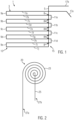
- connection pad 40 in a prelam body (not illustrated) of a smart card (not illustrated) is schematically shown in a top view.
- the wire pad design of Fig. 4 may be formed by routing a wire beginning at the wire end 47a to implement the spiral, triangular shape corresponding to the connection pad wiring pattern 43 shown in Fig. 4 , and further routing the wire underneath or above the wire portions of the connection pad wiring pattern 43 so as to straddle over the connection pad wiring pattern 43 or run below the connection pad wiring pattern 43 at the wire portions.
- the wire portions of the connection pad wiring pattern 53 and/or the bridging wire portion 55 may be made of copper, copper alloy or a copper tin alloy or aluminum or an aluminum alloy, preferably at least some of the plural wire portions of the connection pad wiring pattem 53 and/or the bridging wire portion 55 may be at least partially covered by an insulating coating or may be without any covering.
- a wiring density of the connection pad 50 of as given by a ratio of wire diameter to wire pitch in the connection pad wiring pattern 53 may be in a range from about 0.3 to 0.95.
- a wiring density of the connection pad 60 of as given by a ratio of wire diameter to wire pitch in the connection pad wiring pattern 63 may be in a range from about 0.3 to 0.95.
- connection pad 370 and a connection pad 380 are embedded into the substrate 300 for contacting terminals (not illustrated) of a module (not illustrated), which is to be integrated into the substrate 300.
- each of the connection pads 370 and 380 are realized similar to the connection pad 1 shown in Fig. 1 .
- each of the connection pads 370 and 380 in Fig. 10 is given by a meander like routing pattern.
- at least one of the connection pads 370 and 380 may be replaced by a connection pad according to the connection pads illustrated in Figs. 2 to 6 , instead.
- connection pad wiring pattern 383 this does not pose any limitation on the present disclosure and the person skilled in the art will appreciate that one or more according recesses may be formed at any other connection pad wiring pattern, e.g., at the connection pad wiring pattern 373, as well.
- connection pad wiring pattern may be formed below a connection pad wiring pattern such that wiring portions of the connection pad wiring pattern extend across the one or more additional recesses.
- a wire pad design of a connection pad 401 in a card body of a smart card in accordance with some other illustrative embodiments is schematically illustrated in a top view, whereas Fig. 12 indicates a cross sectional view along line b-b in Fig. 11 .
- Fig. 11 shows the connection pad 401 with a connection pad wiring pattern 403 and a bridging wire portion 405, wherein plural wire portions 407a and 407b of the connection pad wiring pattern 403 define a contacting pad plane.
- the bridging wire portion 405 is located outside the contacting pad plane.
- the bridging wire portion 405 is embedded into a substrate 402 of the prelam body.
- the bridging wire portion 405 may be embedded into a recess (not illustrated) in Fig. 12 prior to the formation of the connection pads wiring pattern 403.
- a recess (not illustrated) is formed in the substrate 402 and the bridging wire portion 405 is embedded into the recess, as shown in Fig. 12 .
- the connection pad wiring pattern 403 is formed on an upper surface of the substrate 402 in the connection pad plane such that the bridging wire portion 405 is located outside the connection pad plane.
- connection pad wiring pattern 403 as shown in Fig. 11 is not limited to a particular shape and the person skilled in the art will appreciate that any of the connection pad wiring patterns 1, 20, 30, 40, and 50 as described with regard to Fig. 1 to 6 above may be used in replacement of the explicitly shown connection pad wiring pattern 403 without departing from this disclosure.
- disclosure of each of the connection pad wiring patterns 1, 20, 30, 40, and 50 as described with regard to Fig. 1 to 6 applies at this point of the description as well, and is incorporated here by reference in its entirety.
- references herein to terms modified by language of approximation such as “about”, “approximately”, and “substantially”, are not to be limited to the precise value specified.
- the language of approximation may correspond to the precision of an instrument used to measure the value and, unless otherwise dependent on the precision of the instrument, may indicate +/- 10% of the stated value(s).
- references herein to terms such as “vertical”, “horizontal”, etc. are made by way of example, and not by way of limitation, to establish a frame of reference.
- the term “horizontal” as used herein is defined as a plane parallel to a conventional plane of a semiconductor substrate, regardless of its actual three-dimensional spatial orientation.
- the terms “vertical” and “normal” refer to a direction perpendicular to the horizontal, as just defined.
- the term “lateral” refers to a direction within the horizontal plane.
- a feature "connected” or “coupled” to or with another feature may be directly connected or coupled to or with the other feature or, instead, one or more intervening features may be present.
- a feature may be “directly connected” or “directly coupled” to or with another feature if intervening features are absent.
- a feature may be “indirectly connected” or “indirectly coupled” to or with another feature if at least one intervening feature is present.
- a feature “on” or “contacting” another feature may be directly on or in direct contact with the other feature or, instead, one or more intervening features may be present.
- a feature may be “directly on” or in “direct contact” with another feature if intervening features are absent.
- a feature may be “indirectly on” or in “indirect contact” with another feature if at least one intervening feature is present.
Landscapes
- Engineering & Computer Science (AREA)
- Microelectronics & Electronic Packaging (AREA)
- Computer Hardware Design (AREA)
- Physics & Mathematics (AREA)
- General Physics & Mathematics (AREA)
- Theoretical Computer Science (AREA)
- Manufacturing Of Printed Wiring (AREA)
- Wire Bonding (AREA)
Claims (15)
- Verbindungspad (1, 10, 20, 30, 40, 50, 60, 70, 80, 210, 220, 370, 380, 401) mit einem Drahtpad-Design für einen Prelam-Körper einer Smartcard (200), wobei das Drahtpad-Design umfasst:ein Verbindungspad-Verdrahtungsmuster (3, 23, 33, 43, 53, 63, 73, 83, 373, 383, 403), das durch mehrere Drahtabschnitte gebildet ist, die sich in einer Verbindungspad-Ebene erstrecken;gekennzeichnet durcheinen Brückendrahtabschnitt (5, 25, 35, 45, 55, 65, 75, 85, 375, 385, 405), der sich zumindest teilweise außerhalb der Verbindungspad-Ebene erstreckt,wobei der Brückendrahtabschnitt mindestens einige der mehreren Drahtabschnitte elektrisch (5, 25, 35, 45, 55, 65, 75, 85, 375, 385, 405) und mechanisch miteinander verbindet.
- Verbindungspad (1, 10, 30, 60, 70, 80, 210, 220, 370, 380, 401) nach Anspruch 1, wobei sich zumindest einige der Drahtabschnitte teilweise parallel erstrecken, wobei ein Abbiegungsabschnitt vorzugsweise zwischen jeweils zwei benachbarten, parallel zueinander verlaufenden Drahtabschnitten angeordnet ist und der Brückendrahtabschnitt (5, 65, 75, 85, 375, 385) vorzugsweise im Wesentlichen quer über die parallelen Drahtabschnitte verläuft.
- Verbindungspad (1, 10, 20, 50, 60, 70, 80, 210, 220, 370, 380) nach Anspruch 1 oder 2, wobei das Verbindungspad-Verdrahtungsmuster (3, 23, 53, 63, 73, 83, 373, 383) ein spiralförmiges Verlegungsmuster oder ein mäanderförmiges Verlegungsmuster oder ein Muster aus mehreren kreisförmigen Formen, die sich teilweise überlappen, und/oder wobei eine Verdrahtungsdichte des Verbindungspad-Verdrahtungsmusters (53, 63) lokal variiert.
- Verbindungspad (1, 10, 20, 30, 40, 50, 60, 70, 80, 210, 220, 370, 380, 401) nach einem der Ansprüche 1 bis 3, wobei ein Verhältnis von Drahtdurchmesser zu Drahtabstand im Verbindungspad-Verdrahtungsmuster (3, 23, 33, 43, 53, 63, 73, 83, 373, 383, 403) in einem Bereich von etwa 0,3 bis etwa 0, 95 liegt, wobei das Verbindungsflächen-Verdrahtungsmuster (3, 23, 33, 43, 53, 63, 73, 83, 373, 383, 403) vorzugsweise mindestens einen ersten Abschnitt aufweist, in dem das Verhältnis im Bereich von etwa 0,3 bis etwa 0, 8 liegt, und mindestens einen zweiten Abschnitt aufweist, in dem das Verhältnis größer als 0,8 und kleiner oder gleich etwa 0,95 ist.
- Verbindungspad (1, 10, 20, 30, 40, 50, 60, 70, 80, 210, 220, 370, 380, 401) nach einem der Ansprüche 1 bis 4, wobei die mehreren Drahtabschnitte einen Drahtabstand von mindestens 300 µm aufweisen und die mehreren Drahtabschnitte einen Durchmesser im einem Bereich von etwa 50 µm bis etwa 300 µm aufweisen, und/oder
wobei mindestens einer der Drahtabschnitte und der Brückendrahtabschnitt (5, 25, 35, 45, 55, 65, 75, 85, 375, 385, 405) aus Kupfer, einer Kupferlegierung oder einer Kupfer-Zinn-Legierung oder Aluminium oder einer Aluminiumlegierung besteht, wobei vorzugsweise mindestens einige der mehreren Drähte zumindest teilweise mit einer isolierenden Beschichtung bedeckt sein können oder ohne jegliche Beschichtung sein können. - Prelam-Körper mit einem Substrat mit mindestens einem in das Substrat (300) eingebetteten Anschlusspad (373, 383), wobei das mindestens eine Anschlusspad gemäß dem Anschlusspad eines der Ansprüche 1 bis 5 ausgebildet ist.
- Prelam-Körper nach Anspruch 6, der ferner eine erste Aussparung (350) umfasst, die in dem Substrat (300) unterhalb des Verbindungspad-Verdrahtungsmusters (383) ausgebildet ist, wobei sich die erste Aussparung (350) zumindest teilweise entlang einer Dickenrichtung des Substrats (300) in das Substrat (300) erstreckt.
- Prelam-Körper nach Anspruch 7, wobei der Brückendrahtabschnitt (385) in der ersten Aussparung (350) aufgenommen ist, wobei der Prelam-Körper vorzugsweise ferner eine zweite Aussparung (355) umfasst, die in dem Substrat (300) unterhalb des Verbindungspad-Verdrahtungsmusters (383) ausgebildet ist, und wobei das Verbindungspad-Verdrahtungsmuster (383) vorzugsweise über mindestens einen Teil der zweiten Aussparung (355) hinweg verläuft.
- Prelam-Körper nach einem der Ansprüche 6 bis 8 in Kombination mit dem Verbindungspad nach Anspruch 2, wobei mindestens ein Abbiegungsabschnitt entfernt ist.
- Prelam-Körper nach einem der Ansprüche 6 bis 9, wobei der Prelam-Körper in einer Draufsicht eine rechteckige Form mit einer Längsabmessung entlang einer Längsrichtung und einer Breitenabmessung aufweist, die kleiner ist als die Längsabmessung entlang einer Breitenrichtung senkrecht zur Längsrichtung in der Draufsicht, wobei Drahtabschnitte relativ zur Breitenabmessung in einem Winkel außerhalb eines Bereichs von etwa 45° bis etwa 90° ausgerichtet sind.
- Smartcard (200), die den Prälam-Körper nach einem der Ansprüche 6 bis 10 und ein in den Prälam-Körper integriertes Modul umfasst, wobei das Modul mindestens einen E/A-Anschluss zum elektrischen Verbinden mit dem mindestens einen Verbindungspad aufweist, wobei das Modul in einem Hohlraum untergebracht ist, der in dem Prälam-Körper benachbart zu dem mindestens einen Verbindungspad vorgesehen ist, so dass der mindestens eine E/A-Anschluss in elektrischen Kontakt mit dem mindestens einen Verbindungspad gebracht wird.
- Smartcard (200) nach Anspruch 11, wobei der elektrische Kontakt zwischen dem mindestens einen E/A-Anschluss und dem mindestens einen Anschlusspad durch mindestens eine der folgenden Verbindungen gebildet ist: eine Lötverbindung, eine Klebeverbindung unter Verwendung einer anisotrop leitfähigen Folie oder einer anisotrop leitfähigen Paste und eine Klebeverbindung unter Verwendung einer isotrop leitfähigen Folie oder einer isotrop leitfähigen Pastenverbindung, und/oder
wobei der Hohlraum an einer Seite des mindestens einen Verbindungspads (1, 10, 20, 30, 40, 50, 60, 70, 80, 210, 220, 370, 380, 401) ausgebildet ist, die von einer Seite des Verbindungspads, an der der Brückendrahtabschnitt (5, 25, 35, 45, 55, 65, 75, 85, 375, 385, 405) ausgebildet ist, abgewandt ist. - Verfahren zum Bilden einer Verbindungspad in einem Prelam-Körper einer Smartcard (200), umfassend:Bereitstellen eines Substrats des Prelam-Körpers;Bilden eines Verbindungspads (1, 10, 20, 30, 40, 50, 60, 70, 80, 210, 220, 370, 380, 401) mit einem Verbindungspad-Verdrahtungsmuster (3, 23, 33, 43, 53, 63, 73, 83 , 373, 383, 403) durch mehrere Drahtabschnitte auf einer Oberfläche des Substrats als Verbindungspad-Ebene; undBilden eines Brückendrahtabschnitts (5, 25, 35, 45, 55, 65, 75, 85, 375, 385, 405), der sich zumindest teilweise außerhalb der Verbindungspad-Ebene erstreckt, wobei der Brückendrahtabschnitt (5, 25, 35, 45, 55, 65, 75, 85, 375, 385, 405) so ausgebildet ist, dass er sich zumindest teilweise über das Verbindungspad-Verdrahtungsmuster (3, 23, 33, 43, 53, 63, 73, 83 , 373, 383, 403) erstreckt.
- Verfahren nach Anspruch 13, das ferner mindestens eines der folgenden Schritte umfasst:Ausbilden einer ersten Aussparung (350) in dem Substrat (300) vor dem Ausbilden des Verbindungspad-Verdrahtungsmusters (383) und des Brückendrahtabschnitts (385), und anschließendes Ausbilden des Brückendrahtabschnitts (385) durch Aufnehmen eines Drahtabschnitts (385) in die erste Aussparung (350), gefolgt vom Ausbilden des Verbindungspad-Verdrahtungsmusters (383) auf der Oberfläche des Substrats (300) außerhalb der ersten Aussparung (350); undBilden einer zweiten Aussparung (355) in dem Substrat (300), wobei die zweite Aussparung (355) zumindest teilweise unterhalb des Verbindungsflächen-Verdrahtungsmusters (383) angeordnet ist und sich die Drahtabschnitte über die zweite Aussparung (355) erstrecken.
- Verfahren zum Bilden einer Smartcard (200), umfassend:Bereitstellen eines Kartenkörpers, der aus einem Prelam-Körper mit mindestens einem darin eingebetteten Verbindungspad (1, 10, 20, 30, 40, 50, 60, 70, 80, 210, 220, 370, 380, 401) gebildet ist, wobei das mindestens eine Verbindungspad (1, 10, 20, 30, 40, 50, 60, 70, 80, 210, 220, 370, 380, 401) durch das Verbindungspad (1, 10, 20, 30, 40, 50, 60, 70, 80, 210, 220, 370, 380, 401) bereitgestellt wird, die gemäß einem der Ansprüche 13 und 14 ausgebildet ist;Bilden eines Hohlraums in dem Kartenkörper durch Fräsen des Hohlraums in den Kartenkörper, um die mindestens eine Verbindungspad (1, 10, 20, 30, 40, 50, 60, 70, 80, 210, 220, 370, 380, 401) freizulegen; undUnterbringen eines Moduls mit mindestens einem E/A-Anschluss in einem Hohlraum neben dem mindestens einen Verbindungspad (1, 10, 20, 30, 40, 50, 60, 70, 80, 210, 220, 370, 380, 401), so dass der mindestens eine E/A-Anschluss in elektrischen Kontakt mit dem mindestens einem Verbindungspad (1, 10, 20, 30, 40, 50, 60, 70, 80, 210, 220, 370, 380, 401) gebracht wird.
Applications Claiming Priority (1)
| Application Number | Priority Date | Filing Date | Title |
|---|---|---|---|
| PCT/IB2021/000828 WO2023026071A1 (en) | 2021-08-27 | 2021-08-27 | Wire pad design of a connection pad in a prelam body of a smart card, prelam body, smart card, method of forming a wire pad design, and method of forming a smart card |
Publications (2)
| Publication Number | Publication Date |
|---|---|
| EP4392895A1 EP4392895A1 (de) | 2024-07-03 |
| EP4392895B1 true EP4392895B1 (de) | 2025-07-02 |
Family
ID=79230726
Family Applications (1)
| Application Number | Title | Priority Date | Filing Date |
|---|---|---|---|
| EP21836225.9A Active EP4392895B1 (de) | 2021-08-27 | 2021-08-27 | Drahtpadentwurf eines anschlusspads in einem vorlam-körper einer chipkarte, vorlam-körper, chipkarte, verfahren zur herstellung eines drahtpadentwurfs und verfahren zur herstellung einer chipkarte |
Country Status (5)
| Country | Link |
|---|---|
| US (1) | US12406167B2 (de) |
| EP (1) | EP4392895B1 (de) |
| KR (1) | KR102842305B1 (de) |
| CN (1) | CN117730325A (de) |
| WO (1) | WO2023026071A1 (de) |
Families Citing this family (1)
| Publication number | Priority date | Publication date | Assignee | Title |
|---|---|---|---|---|
| WO2025133661A1 (en) | 2023-12-21 | 2025-06-26 | Linxens Holding | Pre-laminated structure for a smartcard with non-insulated wire connection |
Family Cites Families (7)
| Publication number | Priority date | Publication date | Assignee | Title |
|---|---|---|---|---|
| US7980477B2 (en) * | 2007-05-17 | 2011-07-19 | Féinics Amatech Teoranta | Dual interface inlays |
| US10733494B2 (en) * | 2014-08-10 | 2020-08-04 | Féinics Amatech Teoranta | Contactless metal card constructions |
| FR3015733B1 (fr) * | 2013-12-23 | 2017-08-25 | Oberthur Technologies | Dispositif electronique, tel qu'une carte, comportant des moyens de contact agences en lacets et procede de fabrication d'un tel dispositif |
| FR3026530B1 (fr) * | 2014-09-30 | 2017-12-22 | Oberthur Technologies | Document electronique a extremites d'antenne inclinees, support d'antenne pour un tel document electronique et procede de fabrication d'un tel document |
| EP3159832B1 (de) * | 2015-10-23 | 2020-08-05 | Nxp B.V. | Authentifizierungstoken |
| EP3716398B1 (de) * | 2017-05-03 | 2026-01-28 | Féinics Amatech Teoranta | Smartcards mit metallfurnier |
| JP6941149B2 (ja) * | 2018-12-06 | 2021-09-29 | エイヴェリー デニソン リテール インフォメーション サービシズ リミテッド ライアビリティ カンパニー | 温度感知rfidデバイスのシールド及び/又は強化 |
-
2021
- 2021-08-27 EP EP21836225.9A patent/EP4392895B1/de active Active
- 2021-08-27 KR KR1020247003507A patent/KR102842305B1/ko active Active
- 2021-08-27 WO PCT/IB2021/000828 patent/WO2023026071A1/en not_active Ceased
- 2021-08-27 US US18/580,019 patent/US12406167B2/en active Active
- 2021-08-27 CN CN202180101033.3A patent/CN117730325A/zh active Pending
Also Published As
| Publication number | Publication date |
|---|---|
| US12406167B2 (en) | 2025-09-02 |
| KR102842305B1 (ko) | 2025-08-04 |
| US20240338547A1 (en) | 2024-10-10 |
| CN117730325A (zh) | 2024-03-19 |
| KR20240019861A (ko) | 2024-02-14 |
| WO2023026071A1 (en) | 2023-03-02 |
| EP4392895A1 (de) | 2024-07-03 |
Similar Documents
| Publication | Publication Date | Title |
|---|---|---|
| US8689428B2 (en) | Method and system for manufacturing an electronic interface apparatus | |
| US7009293B2 (en) | Interconnect substrate, semiconductor device, methods of fabricating, inspecting, and mounting the semiconductor device, circuit board, and electronic instrument | |
| US7958622B1 (en) | Method for making smart cards | |
| US10740670B2 (en) | Methods of fabrication of chip cards and of chip card antenna supports | |
| EP3159831B1 (de) | Dual-interface ic-karte | |
| CN104995642A (zh) | 具有双通信接口的用于芯片卡的简化的电子模块 | |
| EP3813117A1 (de) | Lichtempfindliche anordnung und herstellungsverfahren dafür | |
| KR20210087944A (ko) | 칩 카드용 전자 모듈 | |
| US12361253B2 (en) | Data-bearing card and semi-finished product and wiring layout for same, and method for producing same | |
| US12424528B2 (en) | Module | |
| EP4392895B1 (de) | Drahtpadentwurf eines anschlusspads in einem vorlam-körper einer chipkarte, vorlam-körper, chipkarte, verfahren zur herstellung eines drahtpadentwurfs und verfahren zur herstellung einer chipkarte | |
| EP4490655B1 (de) | Herstellungsartikel in bezug auf ic-module und chipkarten | |
| US20100328189A1 (en) | Process for Electrically Interconnecting Two Components | |
| JP7746991B2 (ja) | カード型媒体 | |
| US10804226B2 (en) | Method for manufacturing chip cards and chip card obtained by said method | |
| US20190245285A1 (en) | Mounting structure, structural component, and method for manufacturing mounting structure | |
| CN117280352A (zh) | 卡形的数据载体以及用于此的半成品和接触排布及其制造方法 | |
| TWI828343B (zh) | 整合至智慧卡的印刷電路、具有印刷電路的智慧卡、及用於智慧卡製造過程的捲對捲式膠帶 | |
| JP4388168B2 (ja) | 樹脂成形基板 | |
| JP2025163729A (ja) | アンテナモジュール | |
| HK40124971A (zh) | 集成电路(ic)模块、多接口ic卡及其形成方法 | |
| HK40119002A (en) | Articles of manufacture relating to ic modules and smart cards | |
| HK40119002B (en) | Articles of manufacture relating to ic modules and smart cards | |
| WO2023085312A1 (ja) | Icモジュール、およびicモジュールの製造方法 | |
| HK40000317B (en) | Methods of fabrication of chip cards and of chip card antenna supports |
Legal Events
| Date | Code | Title | Description |
|---|---|---|---|
| STAA | Information on the status of an ep patent application or granted ep patent |
Free format text: STATUS: UNKNOWN |
|
| STAA | Information on the status of an ep patent application or granted ep patent |
Free format text: STATUS: THE INTERNATIONAL PUBLICATION HAS BEEN MADE |
|
| PUAI | Public reference made under article 153(3) epc to a published international application that has entered the european phase |
Free format text: ORIGINAL CODE: 0009012 |
|
| STAA | Information on the status of an ep patent application or granted ep patent |
Free format text: STATUS: REQUEST FOR EXAMINATION WAS MADE |
|
| 17P | Request for examination filed |
Effective date: 20240326 |
|
| AK | Designated contracting states |
Kind code of ref document: A1 Designated state(s): AL AT BE BG CH CY CZ DE DK EE ES FI FR GB GR HR HU IE IS IT LI LT LU LV MC MK MT NL NO PL PT RO RS SE SI SK SM TR |
|
| DAV | Request for validation of the european patent (deleted) | ||
| DAX | Request for extension of the european patent (deleted) | ||
| GRAP | Despatch of communication of intention to grant a patent |
Free format text: ORIGINAL CODE: EPIDOSNIGR1 |
|
| STAA | Information on the status of an ep patent application or granted ep patent |
Free format text: STATUS: GRANT OF PATENT IS INTENDED |
|
| INTG | Intention to grant announced |
Effective date: 20250415 |
|
| GRAS | Grant fee paid |
Free format text: ORIGINAL CODE: EPIDOSNIGR3 |
|
| P01 | Opt-out of the competence of the unified patent court (upc) registered |
Free format text: CASE NUMBER: APP_19503/2025 Effective date: 20250423 |
|
| GRAA | (expected) grant |
Free format text: ORIGINAL CODE: 0009210 |
|
| STAA | Information on the status of an ep patent application or granted ep patent |
Free format text: STATUS: THE PATENT HAS BEEN GRANTED |
|
| AK | Designated contracting states |
Kind code of ref document: B1 Designated state(s): AL AT BE BG CH CY CZ DE DK EE ES FI FR GB GR HR HU IE IS IT LI LT LU LV MC MK MT NL NO PL PT RO RS SE SI SK SM TR |
|
| REG | Reference to a national code |
Ref country code: GB Ref legal event code: FG4D |
|
| REG | Reference to a national code |
Ref country code: CH Ref legal event code: EP |
|
| REG | Reference to a national code |
Ref country code: DE Ref legal event code: R096 Ref document number: 602021033521 Country of ref document: DE |
|
| REG | Reference to a national code |
Ref country code: NL Ref legal event code: FP Ref country code: IE Ref legal event code: FG4D |
|
| PGFP | Annual fee paid to national office [announced via postgrant information from national office to epo] |
Ref country code: DE Payment date: 20250826 Year of fee payment: 5 |
|
| PGFP | Annual fee paid to national office [announced via postgrant information from national office to epo] |
Ref country code: NL Payment date: 20250828 Year of fee payment: 5 |
|
| PGFP | Annual fee paid to national office [announced via postgrant information from national office to epo] |
Ref country code: GB Payment date: 20250828 Year of fee payment: 5 |
|
| PGFP | Annual fee paid to national office [announced via postgrant information from national office to epo] |
Ref country code: AT Payment date: 20251020 Year of fee payment: 5 Ref country code: FR Payment date: 20250828 Year of fee payment: 5 |
|
| PG25 | Lapsed in a contracting state [announced via postgrant information from national office to epo] |
Ref country code: PT Free format text: LAPSE BECAUSE OF FAILURE TO SUBMIT A TRANSLATION OF THE DESCRIPTION OR TO PAY THE FEE WITHIN THE PRESCRIBED TIME-LIMIT Effective date: 20251103 |
|
| REG | Reference to a national code |
Ref country code: AT Ref legal event code: MK05 Ref document number: 1810066 Country of ref document: AT Kind code of ref document: T Effective date: 20250702 |
|
| PG25 | Lapsed in a contracting state [announced via postgrant information from national office to epo] |
Ref country code: IS Free format text: LAPSE BECAUSE OF FAILURE TO SUBMIT A TRANSLATION OF THE DESCRIPTION OR TO PAY THE FEE WITHIN THE PRESCRIBED TIME-LIMIT Effective date: 20251102 |
|
| PG25 | Lapsed in a contracting state [announced via postgrant information from national office to epo] |
Ref country code: NO Free format text: LAPSE BECAUSE OF FAILURE TO SUBMIT A TRANSLATION OF THE DESCRIPTION OR TO PAY THE FEE WITHIN THE PRESCRIBED TIME-LIMIT Effective date: 20251002 |
|
| REG | Reference to a national code |
Ref country code: LT Ref legal event code: MG9D |
|
| PG25 | Lapsed in a contracting state [announced via postgrant information from national office to epo] |
Ref country code: AT Free format text: LAPSE BECAUSE OF FAILURE TO SUBMIT A TRANSLATION OF THE DESCRIPTION OR TO PAY THE FEE WITHIN THE PRESCRIBED TIME-LIMIT Effective date: 20250702 |
|
| PG25 | Lapsed in a contracting state [announced via postgrant information from national office to epo] |
Ref country code: FI Free format text: LAPSE BECAUSE OF FAILURE TO SUBMIT A TRANSLATION OF THE DESCRIPTION OR TO PAY THE FEE WITHIN THE PRESCRIBED TIME-LIMIT Effective date: 20250702 |
|
| PG25 | Lapsed in a contracting state [announced via postgrant information from national office to epo] |
Ref country code: HR Free format text: LAPSE BECAUSE OF FAILURE TO SUBMIT A TRANSLATION OF THE DESCRIPTION OR TO PAY THE FEE WITHIN THE PRESCRIBED TIME-LIMIT Effective date: 20250702 |
|
| PG25 | Lapsed in a contracting state [announced via postgrant information from national office to epo] |
Ref country code: GR Free format text: LAPSE BECAUSE OF FAILURE TO SUBMIT A TRANSLATION OF THE DESCRIPTION OR TO PAY THE FEE WITHIN THE PRESCRIBED TIME-LIMIT Effective date: 20251003 |
|
| PG25 | Lapsed in a contracting state [announced via postgrant information from national office to epo] |
Ref country code: CZ Free format text: LAPSE BECAUSE OF FAILURE TO SUBMIT A TRANSLATION OF THE DESCRIPTION OR TO PAY THE FEE WITHIN THE PRESCRIBED TIME-LIMIT Effective date: 20250702 Ref country code: SE Free format text: LAPSE BECAUSE OF FAILURE TO SUBMIT A TRANSLATION OF THE DESCRIPTION OR TO PAY THE FEE WITHIN THE PRESCRIBED TIME-LIMIT Effective date: 20250702 |
|
| PG25 | Lapsed in a contracting state [announced via postgrant information from national office to epo] |
Ref country code: LV Free format text: LAPSE BECAUSE OF FAILURE TO SUBMIT A TRANSLATION OF THE DESCRIPTION OR TO PAY THE FEE WITHIN THE PRESCRIBED TIME-LIMIT Effective date: 20250702 |
|
| PG25 | Lapsed in a contracting state [announced via postgrant information from national office to epo] |
Ref country code: PL Free format text: LAPSE BECAUSE OF FAILURE TO SUBMIT A TRANSLATION OF THE DESCRIPTION OR TO PAY THE FEE WITHIN THE PRESCRIBED TIME-LIMIT Effective date: 20250702 Ref country code: BG Free format text: LAPSE BECAUSE OF FAILURE TO SUBMIT A TRANSLATION OF THE DESCRIPTION OR TO PAY THE FEE WITHIN THE PRESCRIBED TIME-LIMIT Effective date: 20250702 |
|
| PG25 | Lapsed in a contracting state [announced via postgrant information from national office to epo] |
Ref country code: RS Free format text: LAPSE BECAUSE OF FAILURE TO SUBMIT A TRANSLATION OF THE DESCRIPTION OR TO PAY THE FEE WITHIN THE PRESCRIBED TIME-LIMIT Effective date: 20251002 |
|
| PG25 | Lapsed in a contracting state [announced via postgrant information from national office to epo] |
Ref country code: ES Free format text: LAPSE BECAUSE OF FAILURE TO SUBMIT A TRANSLATION OF THE DESCRIPTION OR TO PAY THE FEE WITHIN THE PRESCRIBED TIME-LIMIT Effective date: 20250702 |
|
| PG25 | Lapsed in a contracting state [announced via postgrant information from national office to epo] |
Ref country code: RO Free format text: LAPSE BECAUSE OF FAILURE TO SUBMIT A TRANSLATION OF THE DESCRIPTION OR TO PAY THE FEE WITHIN THE PRESCRIBED TIME-LIMIT Effective date: 20250702 |
|
| REG | Reference to a national code |
Ref country code: CH Ref legal event code: H13 Free format text: ST27 STATUS EVENT CODE: U-0-0-H10-H13 (AS PROVIDED BY THE NATIONAL OFFICE) Effective date: 20260324 |
|
| PG25 | Lapsed in a contracting state [announced via postgrant information from national office to epo] |
Ref country code: SM Free format text: LAPSE BECAUSE OF FAILURE TO SUBMIT A TRANSLATION OF THE DESCRIPTION OR TO PAY THE FEE WITHIN THE PRESCRIBED TIME-LIMIT Effective date: 20250702 |
|
| PG25 | Lapsed in a contracting state [announced via postgrant information from national office to epo] |
Ref country code: DK Free format text: LAPSE BECAUSE OF FAILURE TO SUBMIT A TRANSLATION OF THE DESCRIPTION OR TO PAY THE FEE WITHIN THE PRESCRIBED TIME-LIMIT Effective date: 20250702 |
|
| PG25 | Lapsed in a contracting state [announced via postgrant information from national office to epo] |
Ref country code: LU Free format text: LAPSE BECAUSE OF NON-PAYMENT OF DUE FEES Effective date: 20250827 Ref country code: IT Free format text: LAPSE BECAUSE OF FAILURE TO SUBMIT A TRANSLATION OF THE DESCRIPTION OR TO PAY THE FEE WITHIN THE PRESCRIBED TIME-LIMIT Effective date: 20250702 |