EP4383291A2 - Elektronisches bauteil und leiterplatte mit darauf montiertem elektronischen bauteil - Google Patents
Elektronisches bauteil und leiterplatte mit darauf montiertem elektronischen bauteil Download PDFInfo
- Publication number
- EP4383291A2 EP4383291A2 EP23180285.1A EP23180285A EP4383291A2 EP 4383291 A2 EP4383291 A2 EP 4383291A2 EP 23180285 A EP23180285 A EP 23180285A EP 4383291 A2 EP4383291 A2 EP 4383291A2
- Authority
- EP
- European Patent Office
- Prior art keywords
- electronic component
- protrusion
- discharge electrode
- disposed
- width
- Prior art date
- Legal status (The legal status is an assumption and is not a legal conclusion. Google has not performed a legal analysis and makes no representation as to the accuracy of the status listed.)
- Pending
Links
Images




Classifications
-
- H—ELECTRICITY
- H01—ELECTRIC ELEMENTS
- H01G—CAPACITORS; CAPACITORS, RECTIFIERS, DETECTORS, SWITCHING DEVICES, LIGHT-SENSITIVE OR TEMPERATURE-SENSITIVE DEVICES OF THE ELECTROLYTIC TYPE
- H01G2/00—Details of capacitors not covered by a single one of groups H01G4/00-H01G11/00
- H01G2/14—Protection against electric or thermal overload
-
- H—ELECTRICITY
- H05—ELECTRIC TECHNIQUES NOT OTHERWISE PROVIDED FOR
- H05K—PRINTED CIRCUITS; CASINGS OR CONSTRUCTIONAL DETAILS OF ELECTRIC APPARATUS; MANUFACTURE OF ASSEMBLAGES OF ELECTRICAL COMPONENTS
- H05K1/00—Printed circuits
- H05K1/02—Details
- H05K1/0213—Electrical arrangements not otherwise provided for
- H05K1/0216—Reduction of cross-talk, noise or electromagnetic interference
-
- H—ELECTRICITY
- H01—ELECTRIC ELEMENTS
- H01G—CAPACITORS; CAPACITORS, RECTIFIERS, DETECTORS, SWITCHING DEVICES, LIGHT-SENSITIVE OR TEMPERATURE-SENSITIVE DEVICES OF THE ELECTROLYTIC TYPE
- H01G2/00—Details of capacitors not covered by a single one of groups H01G4/00-H01G11/00
- H01G2/02—Mountings
- H01G2/06—Mountings specially adapted for mounting on a printed-circuit support
-
- H—ELECTRICITY
- H01—ELECTRIC ELEMENTS
- H01G—CAPACITORS; CAPACITORS, RECTIFIERS, DETECTORS, SWITCHING DEVICES, LIGHT-SENSITIVE OR TEMPERATURE-SENSITIVE DEVICES OF THE ELECTROLYTIC TYPE
- H01G2/00—Details of capacitors not covered by a single one of groups H01G4/00-H01G11/00
- H01G2/02—Mountings
- H01G2/06—Mountings specially adapted for mounting on a printed-circuit support
- H01G2/065—Mountings specially adapted for mounting on a printed-circuit support for surface mounting, e.g. chip capacitors
-
- H—ELECTRICITY
- H01—ELECTRIC ELEMENTS
- H01G—CAPACITORS; CAPACITORS, RECTIFIERS, DETECTORS, SWITCHING DEVICES, LIGHT-SENSITIVE OR TEMPERATURE-SENSITIVE DEVICES OF THE ELECTROLYTIC TYPE
- H01G4/00—Fixed capacitors; Processes of their manufacture
- H01G4/002—Details
- H01G4/228—Terminals
- H01G4/232—Terminals electrically connecting two or more layers of a stacked or rolled capacitor
-
- H—ELECTRICITY
- H01—ELECTRIC ELEMENTS
- H01G—CAPACITORS; CAPACITORS, RECTIFIERS, DETECTORS, SWITCHING DEVICES, LIGHT-SENSITIVE OR TEMPERATURE-SENSITIVE DEVICES OF THE ELECTROLYTIC TYPE
- H01G4/00—Fixed capacitors; Processes of their manufacture
- H01G4/30—Stacked capacitors
-
- H—ELECTRICITY
- H05—ELECTRIC TECHNIQUES NOT OTHERWISE PROVIDED FOR
- H05K—PRINTED CIRCUITS; CASINGS OR CONSTRUCTIONAL DETAILS OF ELECTRIC APPARATUS; MANUFACTURE OF ASSEMBLAGES OF ELECTRICAL COMPONENTS
- H05K1/00—Printed circuits
- H05K1/02—Details
- H05K1/0213—Electrical arrangements not otherwise provided for
- H05K1/0254—High voltage adaptations; Electrical insulation details; Overvoltage or electrostatic discharge protection ; Arrangements for regulating voltages or for using plural voltages
- H05K1/0257—Overvoltage protection
- H05K1/0259—Electrostatic discharge [ESD] protection
-
- H—ELECTRICITY
- H05—ELECTRIC TECHNIQUES NOT OTHERWISE PROVIDED FOR
- H05K—PRINTED CIRCUITS; CASINGS OR CONSTRUCTIONAL DETAILS OF ELECTRIC APPARATUS; MANUFACTURE OF ASSEMBLAGES OF ELECTRICAL COMPONENTS
- H05K1/00—Printed circuits
- H05K1/18—Printed circuits structurally associated with non-printed electric components
- H05K1/181—Printed circuits structurally associated with non-printed electric components associated with surface mounted components
-
- H—ELECTRICITY
- H01—ELECTRIC ELEMENTS
- H01G—CAPACITORS; CAPACITORS, RECTIFIERS, DETECTORS, SWITCHING DEVICES, LIGHT-SENSITIVE OR TEMPERATURE-SENSITIVE DEVICES OF THE ELECTROLYTIC TYPE
- H01G4/00—Fixed capacitors; Processes of their manufacture
- H01G4/002—Details
- H01G4/228—Terminals
-
- H—ELECTRICITY
- H05—ELECTRIC TECHNIQUES NOT OTHERWISE PROVIDED FOR
- H05K—PRINTED CIRCUITS; CASINGS OR CONSTRUCTIONAL DETAILS OF ELECTRIC APPARATUS; MANUFACTURE OF ASSEMBLAGES OF ELECTRICAL COMPONENTS
- H05K1/00—Printed circuits
- H05K1/02—Details
- H05K1/0213—Electrical arrangements not otherwise provided for
- H05K1/0254—High voltage adaptations; Electrical insulation details; Overvoltage or electrostatic discharge protection ; Arrangements for regulating voltages or for using plural voltages
- H05K1/0257—Overvoltage protection
- H05K1/026—Spark gaps
-
- H—ELECTRICITY
- H05—ELECTRIC TECHNIQUES NOT OTHERWISE PROVIDED FOR
- H05K—PRINTED CIRCUITS; CASINGS OR CONSTRUCTIONAL DETAILS OF ELECTRIC APPARATUS; MANUFACTURE OF ASSEMBLAGES OF ELECTRICAL COMPONENTS
- H05K2201/00—Indexing scheme relating to printed circuits covered by H05K1/00
- H05K2201/10—Details of components or other objects attached to or integrated in a printed circuit board
- H05K2201/10007—Types of components
- H05K2201/10015—Non-printed capacitor
-
- H—ELECTRICITY
- H05—ELECTRIC TECHNIQUES NOT OTHERWISE PROVIDED FOR
- H05K—PRINTED CIRCUITS; CASINGS OR CONSTRUCTIONAL DETAILS OF ELECTRIC APPARATUS; MANUFACTURE OF ASSEMBLAGES OF ELECTRICAL COMPONENTS
- H05K2201/00—Indexing scheme relating to printed circuits covered by H05K1/00
- H05K2201/10—Details of components or other objects attached to or integrated in a printed circuit board
- H05K2201/10613—Details of electrical connections of non-printed components, e.g. special leads
- H05K2201/10621—Components characterised by their electrical contacts
- H05K2201/10636—Leadless chip, e.g. chip capacitor or resistor
Definitions
- the present disclosure relates to an electronic component and a board having the same mounted thereon.
- a multilayer ceramic capacitor (MLCC), a multilayer electronic component, is a chip-type condenser mounted on the printed circuit boards of various types of electronic products such as imaging devices, including a liquid crystal display (LCD) and a plasma display panel (PDP), computers, smartphones, and mobile phones, and serves to charge or discharge electricity therein or therefrom.
- imaging devices including a liquid crystal display (LCD) and a plasma display panel (PDP), computers, smartphones, and mobile phones, and serves to charge or discharge electricity therein or therefrom.
- LCD liquid crystal display
- PDP plasma display panel
- the multilayer ceramic capacitor may be used as a component of various electronic devices due to having a small size, ensuring high capacitance and being easily mounted.
- miniaturization and implementation of high output power in various electronic devices such as computers and mobile devices
- demand for miniaturization and implementation of high capacitance of multilayer ceramic capacitors has also been increasing.
- ESD electrostatic discharge
- An aspect of the present disclosure is to effectively control ESD of a multilayer electronic component by disposing an ESD discharge member on a mounting surface of the multilayer electronic component.
- Another aspect of the present disclosure is to improve space utilization of an electronic component mounted on a board by selectively disposing an ESD discharge member on one surface of a multilayer electronic component.
- Another aspect of the present disclosure is to effectively control ESD depending on an applied voltage, a capacitance of a multilayer electronic component, or the like by allowing a plurality of ESD discharge members to be disposed together with one multilayer electronic component.
- an electronic component may include an ESD discharge member including a substrate having first and second surfaces opposing each other and first and second conductors disposed on the first and second surfaces of the substrate, and a multilayer electronic component disposed on the second surface of the substrate.
- the multilayer electronic component may include a body and first and second external electrodes disposed outside the body and respectively connected to the first and second conductors.
- the first and second conductors may include first and second discharge electrode layers disposed on the second surface of the substrate to be spaced apart from each other and respectively connected to the first and second external electrodes.
- the first discharge electrode layer may have a first protrusion extending in a direction toward the second discharge electrode layer
- the second discharge electrode layer may have a second protrusion extending in a direction toward the first discharge electrode layer.
- An end of the first protrusion may have a shape having a width narrowing in the direction toward the second discharge electrode layer
- an end of the second protrusion may have a shape having a width narrowing in the direction toward the first discharge electrode layer.
- a board having an electronic component mounted thereon may include a printed circuit board including at least one pair of electrode pads thereon, an electronic component disposed on the printed circuit board, and a solder connecting the electrode pad and the electronic component to each other.
- the electronic component may include a multilayer electronic component including a body and first and second external electrodes disposed outside the body, and an ESD discharge member disposed between the multilayer electronic component and the printed circuit board.
- the ESD discharge member may include a substrate having first and second surfaces opposing each other and first and second conductors disposed on the first and second surfaces of the substrate.
- the first and second conductors may include first and second discharge electrode layers disposed on the second surface of the substrate to be spaced apart from each other and respectively connected to the first and second external electrodes.
- the first discharge electrode layer may have a first protrusion extending in a direction toward the second discharge electrode layer
- the second discharge electrode layer may have a second protrusion extending in a direction toward the first discharge electrode layer.
- An end of the first protrusion may have a shape having a width narrowing in the direction toward the second discharge electrode layer
- an end of the second protrusion may have a shape having a width narrowing in the direction toward the first discharge electrode layer.
- an electronic component may include an ESD discharge member including a substrate having first and second surfaces opposing each other and first and second conductors disposed on the first and second surfaces of the substrate; and a multilayer electronic component disposed on the second surface of the substrate.
- the multilayer electronic component may include a body and first and second external electrodes disposed outside the body and respectively connected to the first and second conductors.
- the first and second external electrodes may be spaced apart from each other in a length direction of the body.
- the first and second conductors may include first and second discharge electrode layers disposed on the second surface of the substrate to be spaced apart from each other in the length direction and respectively connected to the first and second external electrodes.
- a gap between the first and second discharge electrode layers in the length direction may be smaller at a center of the substrate than at a side edge of the substrate.
- an electronic component may include an ESD discharge member including a substrate having first and second surfaces opposing each other and first and second conductors disposed on the first and second surfaces of the substrate; and a multilayer electronic component disposed on the second surface of the substrate.
- the multilayer electronic component may include a body and first and second external electrodes disposed outside the body and respectively connected to the first and second conductors.
- the first and second conductors may include first and second discharge electrode layers disposed on the second surface of the substrate, having a gap therebetween, and respectively connected to the first and second external electrodes.
- the first discharge electrode layer may have a first protrusion extending in a direction toward the second discharge electrode layer
- the second discharge electrode layer may have a second protrusion extending in a direction toward the first discharge electrode layer.
- An end of the first protrusion and an end of the second protrusion each may have a tapered shape.
- an ESD discharge member may be disposed on a mounting surface of a multilayer electronic component, thereby effectively controlling ESD of the multilayer electronic component.
- an ESD discharge member may be selectively disposed on one surface of a multilayer electronic component, thereby improving space utilization of an electronic component mounted on a board.
- a plurality of ESD discharge members may be allowed to be disposed together with one multilayer electronic component, thereby effectively controlling ESD depending on an applied voltage, a capacitance of a multilayer electronic component, or the like.
- a first direction may be defined as a thickness (T) direction
- a second direction may be defined as a length (L) direction
- a third direction may be defined as a width (W) direction.
- the thickness (T) direction, the length (L) direction, and the width (W) direction do not refer to a thickness (T), a length (L), and a width (W).
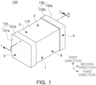
- FIG. 1 is a schematic perspective view of a multilayer electronic component according to an example embodiment of the present disclosure.
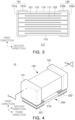
- FIG. 2 is a schematic exploded perspective view of a structure in which the internal electrode of FIG. 1 is stacked.
- FIG. 3 is a schematic cross-sectional view taken along line I-I' of FIG. 1 .
- FIG. 4 is a schematic perspective view of an electronic component according to an example embodiment of the present disclosure.
- FIG. 5 is a schematic perspective view of the ESD discharge member of FIG. 4 .
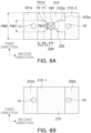
- FIG. 6A is a schematic plan view of a second surface of the ESD discharge member of FIG. 5 in a first direction
- FIG. 6B is a schematic bottom view of a first surface of the ESD discharge member of FIG. 5 in a first direction.
- FIGS. 7A to 7D are schematic plan views of second surfaces of various types of ESD discharge members in a first direction.
- FIG. 8A is a schematic plan view of a second surface of an ESD discharge member having a plurality of protrusions and a plurality of through-holes in a first direction
- FIG. 8B is a schematic bottom view of a first surface of an ESD discharge member having a plurality of protrusions and a plurality of through-holes in a first direction.
- FIG. 9 is a schematic cross-sectional view taken along line II'-II' of FIG. 4 .
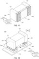
- FIG. 10 is a schematic perspective view of an electronic component according to an example embodiment of the present disclosure.
- FIG. 11 is a schematic perspective view of an electronic component according to an example embodiment of the present disclosure.
- a multilayer ceramic capacitor is described as an example of a multilayer electronic component among electronic components, the present disclosure may be applied to various electronic products using a dielectric composition, such as inductors, piezoelectric elements, varistors, thermistors, or the like.
- an electronic component 10 may include an ESD discharge member 200 including a substrate 210 having first and second surfaces 210-1 and 210-2 opposing each other and first and second conductors 221 and 222 disposed on the first and second surfaces 210-1 and 210-2 of the substrate 210, and a multilayer electronic component 100 disposed on the second surface 210-2 of the substrate 210.
- the multilayer electronic component 100 may include a body 110 and first and second external electrodes 131 and 132 disposed outside the body 110 and respectively connected to the first and second conductors 221 and 222.
- the first and second conductors 221 and 222 may include first and second discharge electrode layers 221a and 222a disposed on the second surface 210-2 of the substrate 210 to be spaced apart from each other and respectively connected to the first and second external electrodes 131 and 132.
- the first discharge electrode layer 221a may have a first protrusion 221a' extending in a direction toward the second discharge electrode layer 222a
- the second discharge electrode layer 222a may have a second protrusion 222a' extending in a direction toward the first discharge electrode layer 221a.
- An end of the first protrusion 221a' may have a shape having a width narrowing in the direction toward the second discharge electrode layer 222a, and an end of the second protrusion 222a' may have a shape having a width narrowing in the direction toward the first discharge electrode layer 221a.
- a dielectric layer 111 and internal electrodes 121 and 122 may be alternately stacked.
- the body 110 may include a capacitance formation portion Ac having capacitance formed by including the first internal electrode 121 and the second internal electrode 122 alternately disposed with the dielectric layer 111 interposed therebetween.
- a specific shape of the body 110 is not particularly limited. However, as illustrated, the body 110 may have a hexahedral shape or a shape similar thereto. During a sintering process, ceramic powder particles included in the body 110 may be shrunken, such that the body 110 may not have a perfectly straight hexahedral shape, but may have a substantially hexahedral shape.
- the body 110 may have first and second surfaces 1 and 2 opposing each other in a first direction, third and fourth surfaces 3 and 4 connected to the first and second surfaces 1 and 2 and opposing each other in a second direction, and fifth and sixth surfaces 5 and 6 connected to the first to fourth surfaces 1, 2, 3, and 4 and opposing each other in a third direction.
- a plurality of dielectric layers 111 included in the body 110 may be in a sintered state, and adjacent dielectric layers 111 may be integrated with each other such that boundaries therebetween are not readily apparent without using a scanning electron microscope (SEM).
- SEM scanning electron microscope
- a raw material included in the dielectric layer 111 is not limited as long as sufficient capacitance is obtainable therewith.
- a perovskite (ABO 3 )-based material may be used.
- a barium titanate-based material, a lead composite perovskite-based material, or a strontium titanate-based material may be used.
- the barium titanate-based material may include BaTiO 3 -based ceramic powder.
- Examples of the ceramic powder may include (Ba 1-x Ca x ) TiO 3 (0 ⁇ x ⁇ 1), Ba(Ti 1-y Ca y )O 3 (0 ⁇ y ⁇ 1), (Ba 1-x Ca x ) (Ti 1-y Zr y )O 3 (0 ⁇ x ⁇ 1, 0 ⁇ y ⁇ 1), or Ba(Ti 1-y Zr y )O 3 (0 ⁇ y ⁇ 1) obtained by partially dissolving Ca or Zr in BaTiO 3 .
- various ceramic additives, organic solvents, binders, and dispersants may be added to powder particles such as barium titanate (BaTiO 3 ), depending on the purpose of the present disclosure.
- a thickness of each of the internal electrodes 121 and 122 is not particularly limited.
- the thickness of each of the internal electrodes 121 and 122 may be 0.6 um or less, and more preferably 0.4 um or less.
- a thickness of the dielectric layer 111 may refer to a thickness of the dielectric layer 111 interposed between the first and second internal electrodes 121 and 122.
- the thickness of the dielectric layer 111 may refer to a size of the dielectric layer 111 in the first direction. In addition, the thickness of the dielectric layer 111 may refer to an average thickness of the dielectric layer 111, and may refer to an average size of the dielectric layer 111 in the first direction.
- the average size of the dielectric layer 111 in the first direction may be measured by scanning, with an SEM, cross-sections of the body 110 in the first and second directions at a magnification of 10,000. More specifically, the average size may be an average value of sizes of one dielectric layer 111 in the first direction, measured at thirty points equally spaced apart from each other in the second direction, in the scanned image. In addition, when such average value measurement is performed on ten dielectric layers 111, the average size of the dielectric layer 111 in the first direction may be further generalized.
- the internal electrodes 121 and 122 may be alternately stacked with the dielectric layer 111.
- the internal electrodes 121 and 122 may include a first internal electrode 121 and a second internal electrode 122, and the first and second internal electrodes 121 and 122 may be alternately disposed to oppose each other with the dielectric layer 111 included in the body 110 interposed therebetween, and may be exposed through the third and fourth surfaces 3 and 4 of the body 110, respectively.
- first internal electrode 121 may be spaced apart from the fourth surface 4, and may be exposed through the third surface 3, and the second internal electrode 122 may be spaced apart from the third surface 3, and may be exposed through the fourth surface 4.
- the first external electrode 131 may be disposed on the third surface 3 of the body 110 to be connected to the first internal electrode 121, and the second external electrode 132 may be disposed on the fourth surface 4 of the body 110 to be connected to the second internal electrode 122.
- first internal electrode 121 may not be connected to the second external electrode 132 and may be connected to the first external electrode 131
- the second internal electrode 122 may not be connected to the first external electrode 131 and may be connected to the second external electrode 132.
- the first and second internal electrodes 121 and 122 may be electrically isolated from each other by the dielectric layer 111 interposed therebetween.
- the body 110 may be formed by alternately stacking a ceramic green sheet on which the first internal electrode 121 is printed and a ceramic green sheet on which the second internal electrode 122 is printed, and then performing sintering thereon.
- a material included in the internal electrodes 121 and 122 is not particularly limited, and a material having excellent electrical conductivity may be used.
- the internal electrodes 121 and 122 may include at least one of nickel (Ni), copper (Cu), palladium (Pd), silver (Ag), gold (Au), platinum (Pt), tin (Sn), tungsten (W), titanium (Ti), and alloys thereof.
- the internal electrodes 121 and 122 may be formed by printing an internal electrode conductive paste including at least one of nickel (Ni), copper (Cu), palladium (Pd), silver (Ag), gold (Au), platinum (Pt), tin (Sn), tungsten (W), titanium (Ti), and alloys thereof, on a ceramic green sheet.
- a screen-printing method or a gravure-printing method may be used as a method for printing the internal electrode conductive paste, but the present disclosure is not limited thereto.
- each of the internal electrodes 121 and 122 is not particularly limited.
- the thickness of each of the internal electrodes 121 and 122 may be 0.6 um or less, and more preferably 0.4 um or less.
- the thickness of each of the internal electrodes 121 and 122 may refer to a size of each of the internal electrodes 121 and 122 in the first direction.
- the thickness of each of the internal electrodes 121 and 122 may refer to an average thickness of each of the internal electrodes 121 and 122, and may refer to an average size of each of the internal electrodes 121 and 122 in the first direction.
- the average size of each of the internal electrodes 121 and 122 in the first direction may be measured by scanning, with an SEM, an image of the cross-sections of the body 110 in the first and second directions at a magnification of 10,000. More specifically, the average size may be an average value of sizes of each of one internal electrode 121 or 122 in the first direction, measured at thirty points equally spaced apart from each other in the second direction, in the scanned image. The thirty points equally spaced apart from each other may be designated in the capacitance formation portion Ac. In addition, when an internal electrode on which such average value measurement is performed is extended to ten internal electrodes, the average size of each of the internal electrodes 121 and 122 in the first direction may be further generalized.
- the body 110 may include cover portions 112 and 113 disposed on both end surfaces of the capacitance formation portion Ac in the first direction.
- the body 110 may include an upper cover portion 112 disposed on an upper portion of the capacitance formation portion Ac in the first direction, and a lower cover portion 113 disposed on a lower portion of the capacitance formation portion Ac in the first direction.
- the upper cover portion 112 and the lower cover portion 113 may be formed by stacking a single dielectric layer 111 or two or more dielectric layers 111 in the first direction in upper and lower surfaces of the capacitance formation portion Ac, respectively, and may basically serve to prevent damage to the internal electrodes 121 and 122 caused by physical or chemical stress.
- the upper cover portion 112 and the lower cover portion 113 may not include the internal electrodes 121 and 122, and may include a material the same as that of the dielectric layer 111. That is, the upper cover portion 112 and the lower cover portion 113 may include a ceramic material, for example, a barium titanate (BaTiO 3 )-based ceramic material.
- a ceramic material for example, a barium titanate (BaTiO 3 )-based ceramic material.
- a thickness of each of the cover portions 112 and 113 is not particularly limited.
- each of the cover portions 112 and 113 may be 100 um or less, preferably 30 um or less, and more preferably 20 um or less in ultra-small products.
- each of the cover portions 112 and 113 may refer to a size of each of the cover portions 112 and 113 in the first direction.
- the thickness of each of the cover portions 112 and 113 may refer to an average thickness of each of the cover portions 112 and 113, and may refer to an average size of each of the cover portions 112 and 113 in the first direction.
- the average size of each of the cover portions 112 and 113 in the first direction may be measured by scanning, with an SEM, an image of the cross-sections of the body 110 in the first and second directions at a magnification of 10,000. More specifically, the average size may be an average value of thicknesses of one cover portion, measured at thirty points equally spaced apart from each other in the second direction, in the scanned image. The thirty points equally spaced apart from each other may be designated in the upper cover portion 112.
- a side margin portion may be disposed on both end surfaces of the body 110 in the third direction.
- the side margin portions may include a first side margin portion disposed on the fifth surface 5 of the body 110 and a second side margin portion disposed on the sixth surface 6 of the body 110. That is, the side margin portion may be disposed on the both end surfaces of the body 110 in the third direction.
- the side margin portion may refer to a region between both ends of the first and second internal electrodes 121 and 122 in the third direction and a boundary surface of the body 110, based on the cross-sections of the body 110 in the second and third direction.
- the side margin portion may basically serve to prevent damage to an internal electrode caused by physical or chemical stress.
- the side margin portion may form the internal electrodes 121 and 122 by applying a conductive paste onto a ceramic green sheet, except a portion in which the side margin portion is to be formed.
- the internal electrodes 121 and 122 may be stacked and cut to be exposed through the fifth and sixth surfaces 5 and 6 of the body 110, and then a single dielectric layer 111 or two or more dielectric layers 111 may be stacked on both end surfaces of the capacitance formation portion Ac in the third direction to form the margin portions 114 and 115.
- a width of each of the first and second side margin portions is not particularly limited.
- the width of each of the first and second side margin portions may be 100 um or less, preferably 30 um or less, and more preferably 20 um or less in ultra-small products.
- a width of the side margin portion may refer to a size of the side margin portion in the third direction.
- the width of the side margin portion may refer to an average width of the side margin portion, and may refer to an average size of the side margin portion in the third direction.
- the average size of the side margin portion in the third direction may be measured by scanning, with an SEM, an image of cross-sections of the body 110 in the first and third directions at a magnification of 10,000. More specifically, the average size may be an average value of sizes of one side margin portion in the third direction, measured at thirty points equally spaced apart from each other in the first direction, in the scanned image. The thirty points equally spaced apart from each other may be designated in the first side margin portion.
- a structure in which a ceramic electronic component 100 has two external electrodes 131 and 132 is described, but the number or shape of the external electrodes 131 and 132 may vary depending on the shape or other purposes of the internal electrodes 121 and 122.
- the external electrodes 131 and 132 may be disposed outside the body 110, and may include first and second external electrodes 131 and 132 respectively connected to first and second conductors 221 and 222 to be described below.
- the external electrodes 131 and 132 may be disposed on the body 110 to be connected to the internal electrodes 121 and 122.
- the external electrodes 131 and 132 may include the first and second external electrodes 131 and 132 disposed on the third and fourth surfaces 3 and 4 of the body 110 and connected to the first and second internal electrodes 121 and 122, respectively. That is, the first external electrode 131 may be disposed on the third surface 3 of the body 110 to be connected to the first internal electrode 121, and the second external electrode 132 may be disposed on the fourth surface 4 of the body 110 to be connected to the second internal electrode 122.
- the first and second external electrodes 131 and 132 may include first and second connection portions 131a and 132a respectively disposed on the third and fourth surfaces 3 and 4 of the body 110, and first and second band portions 131b and 132b extending from the first and second connection portions 131a and 132a to portions of the first, second, fifth and sixth surfaces 1, 2, 5 and 6 of the body 110.
- the first external electrode 131 may include the first connection portion 131a and the first band portion 131b.
- the first connection portion 131a may be disposed on the third surface 3 of the body 110 to be electrically connected to the first internal electrode 121 exposed through the third surface 3 of the body 110.
- the first band portion 131b may be a portion extending from the first connection portion 131a to the portions of the first, second, fifth and sixth surfaces 1, 2, 5 and 6 of the body 110 for improvement in adhesive strength or contact with a first conductor 221.
- the second external electrode 132 may include the second connection portion 132a and the second band portion 132b.
- the second connection portion 132a may be disposed on the fourth surface 4 of the body 110 to be electrically connected to the second internal electrode 122 exposed through the fourth surface 4 of the body 110.
- the second band portion 132b may be a portion extending from the second connection portion 132a to the first, second, fifth, and sixth surfaces 1, 2, 5, and 6 of the body 110 for improvement in adhesive strength or contact with a second conductor 222.
- the external electrodes 131 and 132 may be formed using any material as long as it has electrical conductivity, such as metal, and a specific material may be determined in consideration of electrical properties, structural stability, and the like. Furthermore, the external electrodes 131 and 132 may have a multilayer structure.
- the external electrodes 131 and 132 may include an electrode layer disposed on the body 110 and a plating layer disposed on the electrode layer.
- the electrode layer may be a sintered electrode including a conductive metal and glass, or a resin-based electrode including a conductive metal and resin.
- the electrode layer may have a form in which the sintered electrode and the resin-based electrode are sequentially formed on the body 110.
- the electrode layer may be formed by transferring a sheet including a conductive metal onto the body 110 or by transferring a sheet including a conductive metal onto the sintered electrode.
- the conductive metal used in the electrode layer is not particularly limited as long as it may be electrically connected to the internal electrodes 121 and 122 to form capacitance.
- the conductive metal may include at least one selected from the group consisting of nickel (Ni), copper (Cu), palladium (Pd), silver (Ag), gold (Au), platinum (Pt), tin (Sn), tungsten (W), titanium (Ti), and alloys thereof.
- the electrode layer may be formed by applying a conductive paste prepared by adding a glass frit to the conductive metal powder and then sintering the conductive paste.
- the plating layer may serve to improve mounting properties.
- a type of the plating layer is not particularly limited, and may be a single plating layer including at least one of nickel (Ni), tin (Sn), palladium (Pd), and alloys thereof, and may be formed as a plurality of plating layers.
- the plating layer may be a Ni plating layer or a Sn plating layer, may have a form in which a Ni plating layer and a Sn plating layer are sequentially formed on the electrode layer, and may have a form in which a Sn plating layer, a Ni plating layer, and a Sn plating layer are sequentially formed.
- the plating layer may include a plurality of Ni plating layers and/or a plurality of Sn plating layers.
- An electronic component 10 may include a multilayer electronic component 100 and an ESD discharge member 200.
- the ESD discharge member 200 may include a substrate 210 having first and second surfaces 210-1 and 210-2 opposing each other, and first and second conductors 221 and 222 disposed on the first and second surfaces 210-1 and 210-2 of the substrate 210.
- first and second surfaces 1 and 2 of the body 110 may be different from the first and second surfaces 210-1 and 210-2 of the substrate 210, and respective configurations will be described separately from each other.
- the ESD discharge member 200 may be disposed on one surface of the multilayer electronic component 100.
- the ESD discharge member 200 may be disposed on one surface among the first, second, fifth and sixth surfaces 1, 2, 5, and 6. That is, the ESD discharge member 200 may be disposed on one surface in contact with the first and second band portions 131b and 132b.
- the ESD discharge member 200 may have a length and width less than those of the multilayer electronic component 100. More specifically, the ESD discharge member 200 may be formed inside an outermost point of the electronic component 200 at which the first and second external electrodes 131 and 132 are formed to thereby overlap portions of the first and second band portions 131b and 132b.
- the ESD discharge member 200 may include a substrate 210 having first and second surfaces 210-1 and 210-2 opposing each other, first and second through-holes h1 and h2 passing through the substrate 210, and first and second conductors 221 and 222.
- the multilayer electronic component 100 may be disposed on the second surface 210-2 of the substrate 210, and the first and second external electrodes 131 and 132 may be connected to the first and second conductors 221 and 222, respectively.
- At least one of the first through-hole h1 and the second through-hole h2 may be provided.
- the first through-hole h1 may include a first-first through-hole h1-1 and a first-second through-hole h1-2, and the first-first through-hole h1-1 and the first-second through-hole h1-2 may be spaced apart from each other.
- the second through-portion h2 may include a second-first through-portion h2-1 and a second-second through-portion h2-2, and the second-first through-portion h2-1 and the second-second through-portion h2-2 may be spaced apart from each other.
- the substrate 210 may be formed of a high rigid material, for example, alumina, but the present disclosure is not particularly limited thereto.
- One surface of the multilayer electronic component 100 may be disposed to be in contact with the second surface 210-2 of the substrate.
- the first surface 210-1 of the substrate may be a mounting surface on which the electronic component 10 is in contact with a printed circuit board 600.
- the first and second conductors 221 and 222 may be spaced apart from each other to be symmetrical to each other in the second direction, and may be connected to the first and second external electrodes 131 and 132, respectively.
- the first and second conductors 221 and 222 may be connected to electrode pads 610 and 620 of the printed circuit board 600, respectively, thereby performing a function of connecting, to each other, the multilayer electronic component 100 and the printed circuit board 600.
- the first and second conductors 221 and 222 may be formed by printing a conductive paste on the substrate 210.
- the conductive paste may include at least one of nickel (Ni), copper (Cu), tin (Sn), or alloys thereof.
- the present disclosure is not limited thereto, and the first and second conductors 221 and 222 may be formed by dipping or using other methods such as plating, deposition, and the like.
- the first and second conductors 221 and 222 may be formed to have a constant thickness on at least one surface among the first and second surfaces 210-1 and 210-2 of the substrate.
- the first and second conductors 221 and 222 may be formed flat to have a thickness equal to as that of the surface, as necessary.
- each of the first and second conductors 221 and 222 may refer to a size in the first direction.
- the substrate 210 may have a predetermined step with respect to a region in which the first and second conductors 221 and 222 are to be formed.
- a thickness of the substrate 210 may refer to a thickness of the substrate 210 when the substrate 210 is disposed on a mounting surface of the multilayer electronic component 100, in other words, a size of the substrate 210 in the first direction when the substrate 210 is disposed between the multilayer electronic component 100 and the printed circuit board 600, but the present disclosure is not particularly limited thereto.
- the thickness of the substrate 210 may refer to a size of a space between the first and second surfaces 210-1 and 210-2 of the substrate 210 when the first and second surfaces 210-1 and 210-2 of the substrate 210 are disposed to be parallel to one surface of the body 110.
- the first and second conductors 221 and 222 may be disposed on the second surface 210-2 of the substrate 210 to be spaced apart from each other in the second direction to include first and second discharge electrode layers 221a and 222a respectively connected to the first and second external electrodes 131 and 132, and to include first and second lower-surface electrode layers 221b and 222b disposed on the first surface 210-1 of the substrate 210 to be spaced apart from each other in the second direction.
- a gap between the first and second lower-surface electrode layers 221b and 222b in the second direction may be constant along the third direction.
- first and second through-holes h1 and h2 may be formed in the substrate 210 to be symmetrical to each other in the second direction, and the first and second conductors 221 and 222 may include first and second via electrodes 221c and 222c, respectively covering internal surfaces of the first and second through-holes h1 and h2.
- the first conductor 221 may be disposed to be close to the third surface 3 of the body 110, and may include the first discharge electrode layer 221a, the first lower-surface electrode layer 221b, and the first via electrode 221c.
- the first through-hole h1 may be formed to pass through the first discharge electrode layer 221a, the substrate 210, and the first lower-surface electrode layer 221b.
- the first via electrode 221c covering an internal surface of the first through-hole h1, may connect the first discharge electrode layer 221a and the first lower-surface electrode layer 221b to each other.
- the first conductor 221, an integral body including the first via electrode 221c may include the first lower-surface electrode layer 221b, covering at least a portion of the first surface 210-1 of the substrate 210, and the first discharge electrode layer 221a, covering at least a portion of the second surface 210-2 of the substrate 210.
- the second conductor 222 may be disposed to be close to the fourth surface 4 of the body 110, and may include the second discharge electrode layer 222a, the first lower-surface electrode layer 222b, and the first via electrode 222c.
- the second through-hole h2 may be formed to pass through the second discharge electrode layer 222a, the substrate 210, and the second lower-surface electrode layer 222b.
- the second via electrode 222c covering an internal surface of the second through-hole h2, may connect the second discharge electrode layer 222a and the second lower-surface electrode layer 222b to each other.
- the second conductor 222 an integral body including the second via electrode 222c, may include the second lower-surface electrode layer 222b, covering at least a portion of the first surface 210-1 of the substrate 210, and the second discharge electrode layer 222a, covering at least a portion of the second surface 210-2 of the substrate 210.
- the first and second conductors 221 and 222 may be respectively formed on the first surface 210-1 and the second surface 210-2 of the substrate 210 to be asymmetrical to each other. That is, the first and second lower-surface electrode layers 221b and 222b disposed on the first surface 210-1 of the substrate 210 may be different from the first and second discharge electrode layers 221a and 222a disposed on the second surface 210-2 of the substrate 210.
- the first discharge electrode layer 221a may include a first protrusion 221a' extending in a direction toward the second discharge electrode layer 222a, and the second discharge electrode layer 222a may include a second protrusion 222a' extending in a direction toward the first discharge electrode layer 221a'.
- an end of the first protrusion 221a' may have a shape having a width narrowing in the direction toward the second discharge electrode layer 222a
- an end of the second protrusion 222a' may have a shape having a width narrowing in the direction toward the first discharge electrode layer 221a.
- a gap between the first and second discharge electrode layers 221a and 222a in the second direction may be smaller at a center of the substrate 210 than at a side edge of the substrate 210.
- each of the first and second discharge electrode layers 221a and 222a may be divided into an outer region adjacent to the side edge of the substrate and an inner region adjacent to the center of the substrate.
- the gap between the outer regions of the first and second discharge electrode layers 221a and 222a in the second direction may be constant along the third direction, and the gap between the inner regions of the first and second discharge electrode layers 221a and 222a in the second direction may decrease as the gap approaches the center of the substrate 210 (e.g., FIGS. 7A, 7B, 7D , etc.).
- the gap between the inner regions of the first and second discharge electrode layers 221a and 222a in the second direction may decrease in a linear manner (e.g., FIGS. 6A , 7A, 7B , etc.).
- the gap between the inner regions of the first and second discharge electrode layers 221a and 222a in the second direction may decrease in a nonlinear manner (e.g., FIG. 7D ).
- a step may be formed between the outer region and the inner region such that a maximum gap between the inner regions of the first and second discharge electrode layers 221a and 222a is smaller than the gap between the outer regions of the first and second discharge electrode layers 221a and 222a (e.g., FIGS. 7A and 7D ).
- a maximum gap between the inner regions of the first and second discharge electrode layers 221a and 222a may be equal to the gap between the outer regions of the first and second discharge electrode layers 221a and 222a (e.g., FIG. 7B ).
- an end of the inner region of each of the first and second discharge electrode layers 221a and 222a may have a shape having a sharp point (e.g., FIG. 7A ) .
- an end of the inner region of each of the first and second discharge electrode layers 221a and 222a may have a flat surface (e.g., FISS. 6A, 7B, 7D, etc.).
- both gaps in the outer and inner regions of the first and second discharge electrode layers 221a and 222a may continuously decrease in a linear manner (e.g., FIG. 7C ).
- first protrusion 221a' may include one or more first protrusions and the second protrusion may include one or more second protrusions ( FIG. 8A ).
- first protrusion 221a' may include a first-first protrusion 221a'-1 and a first-second protrusion 221a'-2
- second protrusion 222a' may include a second-first protrusion 222a'-1 and a second-second protrusion 222a'-2.
- first-first protrusion 221a'-1 and the second-first protrusion 222a'-1 may protrude toward each other to be spaced apart from each other with a predetermined first spacer portion 240-1.
- the first-second protrusion 221a'-2 and the second-second protrusion 222a'-2 may protrude toward each other to be spaced apart from each other with a predetermined second spacer portion 240-2.
- first spacer 240-1 and the second spacer 240-2 may have different sizes.
- first and second discharge electrode layers 221a and 222a may include first and second protrusions 221a' and 222a' formed to respectively extend from both ends thereof spaced apart from each other toward a central portion thereof, and a spacer portion 240 formed between the first and second protrusions 221a' and 222a'.
- the first and second protrusions 221a' and 222a' may have a first region P1 having a width decreasing toward each other.
- the first and second discharge electrode layers 221a and 222a may have a "T" shape, and narrow portions formed in the third direction may be formed to oppose each other.
- first and second conductors 221 and 222 may be formed to respectively extend from both ends opposing each other of the second surface 210-2 of the substrate 210 toward a central portion of the second surface 210-2 of the substrate 210. Portions of the first and second discharge electrode layers 221a and 222a disposed to oppose each other toward the central portion of the second surface 210-2 of the substrate 210 may be defined as the first and second protrusions 221a' and 222a'.
- the first and second protrusions 221a' and 222a' may be formed to have a width narrower than that of the substrate 210.
- the end of the first protrusion 221a' may have a shape having a width narrowing in the direction toward the second discharge electrode layer 222a
- the end of the second protrusion 222a' may have a shape having a width narrowing in the direction toward the first discharge electrode layer 221a.
- first and second protrusions 221a' and 222a' may have the first region P1, a region having a width decreasing toward each other.
- a direction of the width may be a direction, perpendicular to the first and second protrusions 221a' and 222a', more specifically, the third direction, but the present disclosure is not particularly limited thereto.
- the width direction when the ESD emitting member is disposed on the fifth or sixth surface 5 or 6 of the multilayer electronic component may refer to the first direction.
- a width of each of the first and second protrusions 221a' and 222a' may refer to a size in the third direction.
- the end of the first protrusion 221a' and the end of the second protrusion 222a' may have a tapered shape.
- the first region P1 may have a tapered shape.
- the tapered shape may mean that inclinations of both side surfaces thereof are symmetrical to each other with respect to a central line thereof.
- the tapered shape may mean that inclinations of both side surfaces are formed to be symmetrical to each other in the third direction with respect to the central line in the second direction.
- a maximum width of each of the first and second discharge electrode layers 221a and 222a is defined as PW0
- a width of one end among the ends of the first and second protrusions is defined as PW12
- a width of the other end among the ends of the first and second protrusions is defined as PW1, 0 ⁇ PW1 ⁇ PW12 ⁇ PW0 may be satisfied.
- a width of one end of the first region P1 may be defined as PW12, and a width of the other end of the first region P1 may be defined as PW1.
- first protrusion 221a' may be described as being the same as one end and the other end of the second protrusion 222a', but the present disclosure is not particularly limited thereto.
- a width of one end of the first protrusion 221a' and a width of one end of the second discharge electrode layer 222a' may be defined as PW12. However, it does not mean that the one end of the first protrusion 221a' and the one end of the second discharge electrode layer 222a' have the same width.
- a width of each of the first protrusion 221a' and the second discharge electrode layers 222a' may be defined as PW12, and descriptions below may also have the same meaning.
- One ends of the first regions P1 of the first and second protrusions 221a' and 222a' may refer to one ends at a short distance from first and second discharge electrode portions 221a and 222b, respectively.
- the other ends of the first regions P1 of the first and second protrusions 221a' and 222a' may refer to the other ends at a short distance from the first and second protrusions 221a' and 222a'.
- one end of the first region P1 of the first protrusion 221a' may refer to one end at a short distance from the first discharge electrode layer 221, and the other end of the first region P1 of the first protrusion 221a' may refer to the other end at a short distance from the other end of the second protrusion 222a'.
- one end of the first region P1 of the second protrusion 222a' may refer to one end at a short distance from the second discharge electrode layer 222, and the other end of the first region P1 of the second protrusion 222a' may refer to the other end at a short distance from the other end of the first protrusion 221a'.
- the one end and the other end may be parallel to each other. That is, one end and the other end of the first region P1 may be parallel to each other.
- a width PW2 of one end and a width PW1 of the other end of the first region P1 may be greater than 0 um, and may have a straight linear shape.
- the two straight lines may be parallel to each other.
- “being parallel to each other” may mean “being substantially parallel to each other,” not “being infinitely parallel to each other, " when two straight lines are extended.
- the width PW1 of the other end of the first region P1 may satisfy 0 ⁇ PW1.
- the width PW1 having a value of "0" may refer to a vertex, and may refer to a vertex or a sharp point ( FIG. 7A ).
- the sharp point may include a vertex forming an angle at a point at which two straight lines meet, and may include a cusp point (sharp point) at which no angular measurement is possible at a point at which two curved lines meet.
- a decrease in width in the first region P1 may include a linear decrease in width ( FIG. 7A ), and may include a width decreasing in a curved shape ( FIG. 7D ), but the present disclosure is not particularly limited thereto, and may refer to anything having a sharp shape.
- an electric field E applied to the multilayer electronic component 100 may be easily gathered into the second protrusions 221a' and 222a', such that electric field concentration (electric intensity) may easily occur, and the concentrated electric field E may be discharged through an ESD discharge portion 240, thereby preventing the multilayer electronic component 100 from being damaged or defects from being occurring in the multilayer electronic component 100, due to the application of high voltage.
- the width PW12 of the other end of the first region P1 may satisfy PW12 ⁇ PW0.
- the width PW12 of the other end of the first region P1 being equal to the maximum width PW0 of each of the first and second discharge electrode layers 221a and 222a may be closer a shape in which the first and second discharge electrode layers 221a and 222a are formed to extend and thereby decrease in width, rather than a shape in which the first and second protrusions 221a' and 222a' protrude from the first and second discharge electrode layers 221a and 222a, but the shape is not particularly limited thereto.
- the width PW12 of the other end of the first region P1 being less than the maximum width (PW0) of each of the first and second discharge electrode layers (PW12 ⁇ PW0) may be closer to a shape in which the first and second protrusions 221a' and 222a' protrude from the first and second discharge electrode layers 221a and 222a, but the shape is not particularly limited thereto.
- the first and second protrusions 221a' and 222a' may have a shape having a constant width.
- a region having a constant width may be defined as a second region P2.
- first and second protrusions 221a' and 222a' may include both the first region P1, a region having a decreasing width, and the second region P2, a region having a constant width.
- first protrusion 221a' may be formed to extend from the first discharge electrode layer 221a, and may have a shape having a width that is constant and then narrows in a direction toward the second discharge electrode layer 222
- second protrusion 222a' may be formed to extend from the second discharge electrode layer 222a, and may have a width that is constant and then narrows in a direction toward the first discharge electrode layer 221a.
- the second regions P2 of the first and second protrusions 221a' and 222a' may have shapes respectively extending from the first and second discharge electrode layers 221 and 222, and the first regions P1 of the first and second protrusions 221a' and 222a' may have shapes respectively extending from the second regions P2.
- a width of the second region P2 is defined as PW2, 0 ⁇ PW1 ⁇ PW12 ⁇ PW2 ⁇ PW0 may be satisfied.
- the second region P2 may be formed to be narrower than the maximum width of each of the first and second discharge electrode layers 221a and 222a, and may have a protruding shape.
- a width PW12 of one end of the first region P1 may be equal to or less than the width PW2 of the second region P2, and may have an extending shape.
- a length PL1 of the first region may be the same or different from a length PL2 of the second region.
- a sharp shape may be more easily formed.
- the length PL2 of the second region is longer than the length PL1 of the first region (PL1 ⁇ PL2), an electric field may be more stably concentrated without the electric field leaking in other directions.
- the present disclosure is not particularly limited thereto, and a structure capable of more easily concentrating the electric field may be sufficient.
- the first and second discharge electrode portions 221a and 222a may be spaced apart from each other.
- a region in which the first and second discharge electrode portions 221a and 222a are spaced apart from each other may be defined as the spacer portion 240.
- first and second protrusions 221a' and 222a' may include the spacer portion 240 formed therebetween.
- the spacer portion 240 may have a shape spaced apart from each other by a predetermined distance from a central portion of the substrate 210, and the predetermined distance may be 1 um or more and 100 um or less.
- a size of the spacer portion 240 may be 1 pm or more and 100 um or less.
- the size of the spacer portion 240 may refer to a size in the second direction.
- the spacer portion 240 may perform a role of ESD by passing.
- a distance (or 'gap' in Fig. 6A ) of the spacer portion 240 between the first and second protrusions 221a' and 222a' may serve to determine an ESD turn-on voltage.
- the turn-on voltage may refer to a voltage at which ESD operates and thereby high-voltage static electricity passes through a lead electrode.
- the concentrated electric field E may not be easily discharged through the ESD discharge portion 230.
- the distance of the spacer portion 240 is greater than 100 ⁇ m, the electric field E may not be easily concentrated, or ESD discharge portion 230 may have an excessively large size, such that a size of the electronic component 10 may increase.
- the distance of the spacer portion 240 is not limited thereto, and the distance may vary depending on the size of the electronic component 10 or the distance may be sufficient as long as it allows ESD discharge to be effectively implemented.
- the ESD discharge member 200 may further include an ESD discharge portion 230 disposed to simultaneously cover the end of the first protrusion 221a', the end of the second protrusion 222a', and the spacer portion 240.
- the ESD discharge portion 230 may be further included to simultaneously cover one end of the first protrusion 221a' , one end of the second protrusion 222a' , and the spacer portion 240.
- the ESD discharge portion 230 is disposed on the second surface 210-2 of the substrate and is formed to simultaneously cover one end of the first and second discharge electrode layers 221a and 222a and the spacer portion 240.
- the ESD discharge portion 230 may be formed by printing ESD paste on the substrate 210.
- the ESD paste may be formed by mixing a conductive material and an insulating material.
- the conductive material included in the ESD paste may include, for example, at least one of copper (Cu), silver (Ag), palladium (Pd), tin (Sn), nickel (Ni), gold (Au), and alloys thereof, but the present disclosure is not particularly limited thereto.
- the insulating material included in the ESD paste may include, for example, a resin such as epoxy or the like, but the present disclosure is not particularly limited thereto.
- At least one ESD discharge portion 230 may be provided.
- the ESD discharge portion 230 may include a first discharge portion 230-1 and a second discharge portion 230-2.
- the first discharge portion 230-1 may simultaneously cover the first-first protrusion 221a'-1, the second-first protrusion 222a'-2, and the first spacer portion 240-1.
- the second discharge portion 230-2 may simultaneously cover the first-second protrusion 221a'-2, the second-second protrusion 222a'-2, and the second spacer portion 240-2.
- the ESD discharge portion 230 may include a conductive polymer.
- the conductive polymer may have properties of a nonconductor when a signal voltage input from a signal interface through which a signal is transmitted from a connector to a system or IC, an IC block of a power terminal, or a communication line is on a rated voltage (circuit voltage) level, or may have properties of a conductor when an overvoltage such as ESD occurs instantaneously.
- the first and second conductors 221 and 222 may include first and second lower-surface electrode layers 221b and 222b disposed on the first surface 210-1 of the substrate to be spaced apart from each other.
- first and second lower-surface electrode layers 221b and 222b disposed on the first surface 210-1 of the substrate may have various shapes, for example, may respectively have rectangular shapes, and the first and second lower-surface electrode layers 221b and 222b may be spaced apart from each other in the second direction without forming a protrusion, but the present disclosure is not particularly limited thereto.
- first and second lower-surface electrode layers 221b and 222b may be disposed to respectively overlap the first and second discharge electrode layers 221a and 222a in the first direction.
- the first and second conductors 221 and 222 may not be formed on a side surface, perpendicular to the first and second surfaces 210-1 and 210-2 of the substrate.
- first and second conductors 221 and 222 may be respectively formed on the first and second surfaces 210-1 and 210-2 of the substrate, and internal surfaces of the first and second through-holes h1 and h2.
- first and second conductors 221 and 222 may not be respectively formed on both side surfaces of the substrate 210 in the second direction and both side surfaces of the substrate 210 in the third direction.
- the multilayer electronic component 100 may be an open circuit in DC power. However, when a crack occurs in the body 110 due to an external environment, the internal electrodes 121 and 122 may overlap each other or a current path may be generated, resulting in a defect caused by a short circuit. The defect caused by the short circuit may cause overcurrent to flow through undesigned lines, which may adversely affect other components.
- a margin on a side of an external electrode which is prone to cracks due to external force, was designed to increase such that a short circuit between both electrodes of an internal electrode does not occur even when a crack occurs.
- an area of the internal electrode implementing capacitance may be relatively reduced.
- the ESD discharge member 200 may be attached to one surface of the multilayer electronic component 100 to provide an ESD bypassing function such as an ESD suppressor, thereby implementing an ESD protection function without changing a design of internal electrodes of a multilayer electronic component.
- overvoltage of the ESD may be controlled by adjusting a distance of the spacer portion 240, a distance between the first and second discharge electrode layers 221a and 222a, or by forming the ESD discharge portion 230.
- high voltage introduced from the printed circuit board 600 to the multilayer electronic component 100 may flow through the first and second discharge electrode layers 221a and 222a, and then may flow out through the ESD discharge portion 230 formed on the spaced portion 240, thereby preventing the multilayer electronic component 100 from being damaged or defects from being occurring in the multilayer electronic component 100, due to the application of high voltage.
- the electronic component 10 may further include first and second conductive bonding layers 310 and 320 disposed between the first and second external electrodes 131 and 132 and the ESD discharge member 200, respectively.
- the multilayer electronic component 100 and the ESD discharge member 200 may be bonded through the first and second conductive bonding layers 310 and 320, and more specifically, the first and second external electrodes 131 and 132 and the first and second discharge electrode layers 221a and 222a may be connected by first and second conductive bonding layers 310 and 320, respectively.
- the first and second conductive bonding layers 310 and 320 may bond portions of the first and second discharge electrode layers 221a and 222a and portions of the first and second band portions 131b and 132b to each other.
- the first and second conductive bonding layers 310 and 320 may fill at least portions of the first and second through-holes h1 and h2, but the present disclosure is not particularly limited thereto, and the first and second conductive bonding layers 310 and 320 may be disposed only in portions in which the first and second through-holes h1 and h2 are not formed.
- the first and second conductive bonding layers 310 and 320 are not particularly limited, but may include, for example, a conductive metal or resin.
- the first and second external electrodes 131 and 132 and the first and second conductors 221 and 222 may be electrically connected to each other, while bonding strength between the multilayer electronic component 100 and the ESD discharge member 200 may be improved, thereby performing a function of increasing adhesive strength.
- the ESD discharge member may include at least one ESD discharge member.
- the at least one ESD discharge member may be in contact with the first and second band portions 131b and 132b, and may be disposed on one or more surfaces selected from the first, second, fifth, and sixth surfaces 1, 2, 5, and 6.
- the ESD discharge member 200 may be coupled to one surface on which the first surface 1 of the body 110 is disposed, that is, a mounting surface of the multilayer electronic component 100, to be in contact therewith.
- the ESD discharge member 200 when the electronic component 10 is mounted on the printed circuit board 600, the ESD discharge member 200 may be disposed between the multilayer electronic component 100 and the printed circuit board 600.
- solders 710 and 720, fixing the electronic component 10 to the printed circuit board 600 may be disposed between the first surface 210-1 of the substrate of the ESD discharge member 200 and the printed circuit board 600.
- a portion of the solders 710 and 720 applied to the first surface 210-1 of the substrate may be disposed to fill at least portions of internal spaces of the first and second through-holes h1 and h2 provided in the substrate 210.
- a bonding area between the solders 710 and 720 and the ESD discharge member 200 may be increased, thereby increasing adhesive strength between the printed circuit board 600 and the electronic component 10.
- the ESD discharge member 200 may be coupled to the other surface, not the mounting surface of the multilayer electronic component 100, to be in contact therewith.
- one ESD discharge member 500 may be disposed on the sixth surface 6 of the body 100 to be in contact with the first and second band portions 131b and 132b.
- first and second lower-surface electrode layers of the first and second conductors 521 and 522 disposed on a first surface of a substrate of the ESD discharge member 500 may be coupled toward the outside of the multilayer electronic component 100.
- the plurality of ESD discharge members may be coupled to the first and second band portions 131b and 132b, respectively, on two or more surfaces among surfaces on which the first, second, fifth, and sixth surfaces 1, 2, 5, and 6 of the body 110 are disposed.
- the number of the plurality of ESD discharge members coupled to one multilayer electronic component 100 is not particularly limited, and a position in which the plurality of ESD discharge members are disposed is also not particularly limited.
- the ESD discharge members 200 and 400 may be disposed on surfaces opposing each other of the multilayer electronic component 100, respectively.
- one ESD discharge member 200 may be disposed on the first surface 1, the mounting surface of the multilayer electronic component 100, and may correspond to a high-voltage ESD discharge member 200.
- Another ESD discharge member 400 may be disposed on the second surface 20 of the multilayer electronic component 100, and may correspond to a low-voltage ESD discharge member 400.
- a high-voltage ESD discharge member may be disposed on one surface of the multilayer electronic component 100, and a low voltage ESD discharge member may be disposed on the other surface, and thus may be applicable to the electronic component 10 having ESD voltage covering a wider range.
- the plurality of ESD discharge members may not need to be disposed on surfaces opposing each other of the multilayer electronic component 100, and the plurality of ESD discharge members may be freely disposed on two or more surfaces selected from among the first, second, fifth, and sixth surfaces of the body 110.
- an ESD discharge member may be freely disposed on one surface of the multilayer electronic component 100, thereby increasing space utilization of the electronic component 10 mounted on the printed circuit board 600.
- FIG. 12 is a schematic perspective view of a board having an electronic component mounted thereon according to an example embodiment in which the electronic component of FIG. 4 is disposed on a printed circuit board.
- FIG. 13 is a schematic cross-sectional view taken along line III'-III' of FIG. 12 .
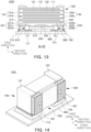
- FIG. 14 is a schematic perspective view of a board having an electronic component mounted thereon, the electronic component obtained by additionally disposing an ESD discharge member on the electronic component of FIG. 12 .
- a board 1000 having an electronic component mounted thereon may include a printed circuit board 600 including at least one pair of electrode pads 610 and 620 thereon, an electronic component 10 disposed on the printed circuit board 600, and solders 710 and 720 connecting the electrode pads 610 and 620 and the electronic component 10 to each other.
- the electronic component 10 include a multilayer electronic component 100 including a body 110 and first and second external electrodes 131 and 132 disposed outside the body 110, and an ESD discharge member 200 disposed between the multilayer electronic component 100 and the printed circuit board 600.
- the ESD discharge member 200 may include the ESD discharge member 200 including a substrate 210 having first and second surfaces 210-1 and 210-2 opposing each other and first and second conductors 221 and 222 disposed on the first and second surfaces 210-1 and 210-2 of the substrate 210, and the multilayer electronic component 100 disposed on the second surface 210-2 of the substrate 210.
- the multilayer electronic component 100 may include a body 110 and first and second external electrodes 131 and 132 disposed outside the body 110 and respectively connected to the first and second conductors 221 and 222.
- the first and second conductors 221 and 222 may include first and second discharge electrode layers 221a and 222a disposed on the second surface 210-2 of the substrate 210 to be spaced apart from each other and respectively connected to the first and second external electrodes 131 and 132.
- the first and second discharge electrode layers 221a and 222a may have first and second protrusions 221a' and 222a' respectively extending from both ends thereof spaced apart from each other toward a central portion thereof, and a spacer portion 240 formed between the first and second protrusions 221a' and 222a'.
- the first and second protrusions 221a' and 222a' may have a first region P1, a region having a width decreasing toward each other.
- the pair of electrode pads 610 and 620 may include first and second electrode pads 610 and 620 respectively connected to the first and second conductors 221 and 222 of the ESD discharge member 200 of the electronic component 10.
- the printed circuit board 600 and the ESD discharge member 200 may be connected to each other by the solders 710 and 720.
- the solders 710 and 720 may be disposed to cover various regions.
- the solders 710 and 720 may be disposed between the first and second electrode pads 610 and 620 and the first and second lower-surface electrode layers 221b and 222b, respectively.
- solders 710 and 720 may include a first solder 710 disposed between a first electrode pad 610 and a first lower-surface electrode layer 221b, and a second solder 720 disposed between a second electrode pad 620 and a second lower-surface electrode layer 222b.
- solders 710 and 720 may be disposed to fill at least portions of the internal space of the first and second through-holes h1 and h2.
- volumes and shapes of the solders 711 and 721 disposed in internal spaces of the first and second through-holes h1 and h2 may vary, and the solders 711 and 721 having different volumes and shapes may be formed to be irregular in shape.
- solders 711 and 721 may be disposed to fill at least portions of the internal spaces of the first and second through-holes h1 and h2, such that a contact area between the multilayer electronic component 100 and the solders 710 and 720, bonding the printed circuit board 600 including the first and second electrode pads 610 and 620 and the ESD discharge member 200 to each other, may be increased, thereby further improving adhesive strength of the electronic component 10.
- first and second through-holes h1 and h2 provided in the first and second lower-surface electrode layers 221b and 222b may be partially filled with solders 711 and 721 having conductivity, thereby improving electrical connectivity between the first and second conductors 221 and 222.
- solders 711 and 721 disposed in the internal spaces of the first and second through-holes h1 and h2 do not necessarily need to be included. In some example embodiments, only one or both of the solders 711 and 721 may be included, or none of the solders 711 and 721 may be included.
- the solders 710 and 720 may not be in contact with the multilayer electronic component 100. That is, the solders 710 and 720 may be formed to have a size less than equal to half of a size of each of the first and second through-holes h1 and h2 in the first direction, with respect to cross-sections of the ESD discharge member 200 in the first and second directions. In a region in which the solders 710 and 720 have a size greater than half of the size of each of the first and second through-holes h1 and h2 in the first direction, the solders 710 and 720 may no longer be formed. Accordingly, the solders 710 and 720 may not be in contact with the first and second external electrodes 131 and 132 of the multilayer electronic component 100 positioned above the ESD discharge member 200.
- the solders 710 and 720 may have relatively strong attractive force acting on the first and second lower-surface electrode layers 221b and 222b having a material similar to that of the solder 710 and 720. Conversely, the solders 710 and 720 may have relatively weak attractive force acting on the substrate 210 of the ESD discharge member 200 having a material different from that of the solders 710 and 720.
- solders 710 and 720 it is possible to suppress the solders 710 and 720 from being formed upwardly in the first direction with respect to cross-sections of the substrate 210 in the first and second directions, and to reduce a degree of vibrations being transferred to the printed circuit board 600 by the solders 710 and 720.
- the shapes of the solders 710 and 720 are not limited thereto.
- the solders 710 and 720 may be in contact with the multilayer electronic component 100, but may have a small contact area with the multilayer electronic component 100.
- the solders 710 and 720 may be formed in a region in which the solders 710 and 720 have a size greater than half of the size of each of the first and second through-holes h1 and h2 in the first direction, with respect to the cross-sections of the substrate 210 in the first and second directions.
- the solders 710 and 720 may reach the multilayer electronic component 100 through the ESD discharge member 200, such that a contact area between the solders 710 and 720 and the multilayer electronic component 100 may be narrow as compared to an electronic component not including the ESD discharge member 200 according to the related art.
- the electronic component 10 may include the ESD discharge member 200, such that an amount of solder fillet formed around the electronic component may be reduced.
- the number of vibrations transferred to the printed circuit board 600 may be reduced, thereby reducing acoustic noise.
- a board 1001 having an electronic component mounted thereon may include a plurality of ESD discharge members 200 and 500.
- ESD discharge members may be disposed on at least two surfaces of the multilayer electronic component 100, respectively.
- one ESD discharge member 200 may be disposed between the multilayer electronic component 100 and the printed circuit board 600, and another ESD discharge member 500 may be disposed on the sixth surface 6 of the body 110.
- an ESD discharge member may be disposed on at least one of the first, second, fifth, and sixth surfaces of the body 110.
- the solders 711 and 721 may be disposed to fill at least portions of internal spaces of the first and second through-holes h1 and h2 of the ESD discharge member 200. Volumes and shapes of the solders 710 and 720 disposed in the internal spaces of the first and second through-holes h1 and h2 may vary, and the solders 710 and 720 having different volumes and shapes may be formed to be irregular in shape.
Landscapes
- Engineering & Computer Science (AREA)
- Power Engineering (AREA)
- Microelectronics & Electronic Packaging (AREA)
- Manufacturing & Machinery (AREA)
- Physics & Mathematics (AREA)
- Electromagnetism (AREA)
- Fixed Capacitors And Capacitor Manufacturing Machines (AREA)
- Ceramic Capacitors (AREA)
- Thermistors And Varistors (AREA)
Applications Claiming Priority (1)
| Application Number | Priority Date | Filing Date | Title |
|---|---|---|---|
| KR1020220170253A KR20240085419A (ko) | 2022-12-08 | 2022-12-08 | 전자 부품 및 그 실장 기판 |
Publications (2)
| Publication Number | Publication Date |
|---|---|
| EP4383291A2 true EP4383291A2 (de) | 2024-06-12 |
| EP4383291A3 EP4383291A3 (de) | 2024-08-28 |
Family
ID=86904256
Family Applications (1)
| Application Number | Title | Priority Date | Filing Date |
|---|---|---|---|
| EP23180285.1A Pending EP4383291A3 (de) | 2022-12-08 | 2023-06-20 | Elektronisches bauteil und leiterplatte mit darauf montiertem elektronischen bauteil |
Country Status (5)
| Country | Link |
|---|---|
| US (1) | US20240196523A1 (de) |
| EP (1) | EP4383291A3 (de) |
| JP (1) | JP2024083221A (de) |
| KR (1) | KR20240085419A (de) |
| CN (1) | CN118175722A (de) |
Family Cites Families (5)
| Publication number | Priority date | Publication date | Assignee | Title |
|---|---|---|---|---|
| JP2000114005A (ja) * | 1998-10-06 | 2000-04-21 | Murata Mfg Co Ltd | セラミック電子部品 |
| JP5093345B2 (ja) * | 2008-05-08 | 2012-12-12 | 株式会社村田製作所 | Esd保護機能内蔵基板 |
| US8885324B2 (en) * | 2011-07-08 | 2014-11-11 | Kemet Electronics Corporation | Overvoltage protection component |
| KR101808794B1 (ko) * | 2015-05-07 | 2018-01-18 | 주식회사 모다이노칩 | 적층체 소자 |
| KR20220084658A (ko) * | 2020-12-14 | 2022-06-21 | 삼성전기주식회사 | 전자 부품 |
-
2022
- 2022-12-08 KR KR1020220170253A patent/KR20240085419A/ko active Pending
-
2023
- 2023-06-20 EP EP23180285.1A patent/EP4383291A3/de active Pending
- 2023-06-22 US US18/213,005 patent/US20240196523A1/en active Pending
- 2023-06-29 JP JP2023107326A patent/JP2024083221A/ja active Pending
- 2023-09-20 CN CN202311215695.0A patent/CN118175722A/zh active Pending
Also Published As
| Publication number | Publication date |
|---|---|
| KR20240085419A (ko) | 2024-06-17 |
| JP2024083221A (ja) | 2024-06-20 |
| US20240196523A1 (en) | 2024-06-13 |
| EP4383291A3 (de) | 2024-08-28 |
| CN118175722A (zh) | 2024-06-11 |
Similar Documents
| Publication | Publication Date | Title |
|---|---|---|
| KR101548774B1 (ko) | 적층 세라믹 커패시터 | |
| KR102586070B1 (ko) | 적층 세라믹 전자부품 | |
| KR20140038871A (ko) | 적층 세라믹 커패시터 및 그 실장 기판 | |
| US11094467B2 (en) | Multilayer ceramic capacitor and board having the same | |
| CN115116746B (zh) | 电容器组件 | |
| CN109903992B (zh) | 复合电子组件 | |
| CN104810150A (zh) | 多层陶瓷电容器和其上安装有多层陶瓷电容器的板 | |
| KR20150019732A (ko) | 적층 세라믹 커패시터 및 적층 세라믹 커패시터 실장 기판 | |
| US12020869B2 (en) | Multilayer electronic component having improved electrode structure for increased capacity per unit volume | |
| EP4383291A2 (de) | Elektronisches bauteil und leiterplatte mit darauf montiertem elektronischen bauteil | |
| KR20190121218A (ko) | 적층 세라믹 전자부품 | |
| CN111180207B (zh) | 多层陶瓷电子组件和多层陶瓷电子组件封装件 | |
| US12176153B2 (en) | Multilayer electronic component | |
| US12374497B2 (en) | Multilayer electronic component with improved reliability | |
| US12374496B2 (en) | Multilayer electronic component | |
| US12198860B2 (en) | Multilayer electronic component and method of manufacturing the same | |
| US11581147B2 (en) | Electronic component | |
| KR102145316B1 (ko) | 적층 세라믹 커패시터 및 그 실장 기판 | |
| JP2023143583A (ja) | 積層型キャパシタ及びその内蔵基板 | |
| KR102004779B1 (ko) | 적층 세라믹 전자부품 및 그 실장 기판 | |
| KR20220056402A (ko) | 전자 부품 및 그 실장 기판 | |
| US12112892B2 (en) | Multilayer electronic component | |
| US20250201480A1 (en) | Multilayer electronic component | |
| US20250166896A1 (en) | Multilayer electronic component and board having multilayer electronic component mounted thereon |
Legal Events
| Date | Code | Title | Description |
|---|---|---|---|
| PUAI | Public reference made under article 153(3) epc to a published international application that has entered the european phase |
Free format text: ORIGINAL CODE: 0009012 |
|
| STAA | Information on the status of an ep patent application or granted ep patent |
Free format text: STATUS: THE APPLICATION HAS BEEN PUBLISHED |
|
| AK | Designated contracting states |
Kind code of ref document: A2 Designated state(s): AL AT BE BG CH CY CZ DE DK EE ES FI FR GB GR HR HU IE IS IT LI LT LU LV MC ME MK MT NL NO PL PT RO RS SE SI SK SM TR |
|
| PUAL | Search report despatched |
Free format text: ORIGINAL CODE: 0009013 |
|
| AK | Designated contracting states |
Kind code of ref document: A3 Designated state(s): AL AT BE BG CH CY CZ DE DK EE ES FI FR GB GR HR HU IE IS IT LI LT LU LV MC ME MK MT NL NO PL PT RO RS SE SI SK SM TR |
|
| RIC1 | Information provided on ipc code assigned before grant |
Ipc: H01G 4/228 20060101ALN20240719BHEP Ipc: H05K 1/18 20060101ALI20240719BHEP Ipc: H05K 1/11 20060101ALI20240719BHEP Ipc: H05K 1/02 20060101ALI20240719BHEP Ipc: H01G 4/30 20060101ALI20240719BHEP Ipc: H01G 4/232 20060101ALI20240719BHEP Ipc: H01G 2/06 20060101ALI20240719BHEP Ipc: H01G 2/14 20060101AFI20240719BHEP |
|
| STAA | Information on the status of an ep patent application or granted ep patent |
Free format text: STATUS: REQUEST FOR EXAMINATION WAS MADE |
|
| 17P | Request for examination filed |
Effective date: 20250226 |