EP4380071A2 - Adressierung für integrierte schaltungen - Google Patents
Adressierung für integrierte schaltungen Download PDFInfo
- Publication number
- EP4380071A2 EP4380071A2 EP23209640.4A EP23209640A EP4380071A2 EP 4380071 A2 EP4380071 A2 EP 4380071A2 EP 23209640 A EP23209640 A EP 23209640A EP 4380071 A2 EP4380071 A2 EP 4380071A2
- Authority
- EP
- European Patent Office
- Prior art keywords
- integrated circuit
- beamformer integrated
- address
- beamformer
- set state
- Prior art date
- Legal status (The legal status is an assumption and is not a legal conclusion. Google has not performed a legal analysis and makes no representation as to the accuracy of the status listed.)
- Pending
Links
Images



Classifications
-
- H—ELECTRICITY
- H03—ELECTRONIC CIRCUITRY
- H03K—PULSE TECHNIQUE
- H03K19/00—Logic circuits, i.e. having at least two inputs acting on one output; Inverting circuits
- H03K19/0175—Coupling arrangements; Interface arrangements
- H03K19/0185—Coupling arrangements; Interface arrangements using field effect transistors only
- H03K19/018585—Coupling arrangements; Interface arrangements using field effect transistors only programmable
-
- H—ELECTRICITY
- H04—ELECTRIC COMMUNICATION TECHNIQUE
- H04B—TRANSMISSION
- H04B7/00—Radio transmission systems, i.e. using radiation field
- H04B7/02—Diversity systems; Multi-antenna system, i.e. transmission or reception using multiple antennas
- H04B7/04—Diversity systems; Multi-antenna system, i.e. transmission or reception using multiple antennas using two or more spaced independent antennas
- H04B7/06—Diversity systems; Multi-antenna system, i.e. transmission or reception using multiple antennas using two or more spaced independent antennas at the transmitting station
- H04B7/0613—Diversity systems; Multi-antenna system, i.e. transmission or reception using multiple antennas using two or more spaced independent antennas at the transmitting station using simultaneous transmission
- H04B7/0615—Diversity systems; Multi-antenna system, i.e. transmission or reception using multiple antennas using two or more spaced independent antennas at the transmitting station using simultaneous transmission of weighted versions of same signal
- H04B7/0617—Diversity systems; Multi-antenna system, i.e. transmission or reception using multiple antennas using two or more spaced independent antennas at the transmitting station using simultaneous transmission of weighted versions of same signal for beam forming
-
- H—ELECTRICITY
- H01—ELECTRIC ELEMENTS
- H01Q—ANTENNAS, i.e. RADIO AERIALS
- H01Q3/00—Arrangements for changing or varying the orientation or the shape of the directional pattern of the waves radiated from an antenna or antenna system
- H01Q3/26—Arrangements for changing or varying the orientation or the shape of the directional pattern of the waves radiated from an antenna or antenna system varying the relative phase or relative amplitude of energisation between two or more active radiating elements; varying the distribution of energy across a radiating aperture
- H01Q3/30—Arrangements for changing or varying the orientation or the shape of the directional pattern of the waves radiated from an antenna or antenna system varying the relative phase or relative amplitude of energisation between two or more active radiating elements; varying the distribution of energy across a radiating aperture varying the relative phase between the radiating elements of an array
- H01Q3/34—Arrangements for changing or varying the orientation or the shape of the directional pattern of the waves radiated from an antenna or antenna system varying the relative phase or relative amplitude of energisation between two or more active radiating elements; varying the distribution of energy across a radiating aperture varying the relative phase between the radiating elements of an array by electrical means
-
- H—ELECTRICITY
- H03—ELECTRONIC CIRCUITRY
- H03K—PULSE TECHNIQUE
- H03K19/00—Logic circuits, i.e. having at least two inputs acting on one output; Inverting circuits
- H03K19/02—Logic circuits, i.e. having at least two inputs acting on one output; Inverting circuits using specified components
- H03K19/08—Logic circuits, i.e. having at least two inputs acting on one output; Inverting circuits using specified components using semiconductor devices
- H03K19/094—Logic circuits, i.e. having at least two inputs acting on one output; Inverting circuits using specified components using semiconductor devices using field-effect transistors
- H03K19/09425—Multistate logic
-
- H—ELECTRICITY
- H03—ELECTRONIC CIRCUITRY
- H03K—PULSE TECHNIQUE
- H03K19/00—Logic circuits, i.e. having at least two inputs acting on one output; Inverting circuits
- H03K19/02—Logic circuits, i.e. having at least two inputs acting on one output; Inverting circuits using specified components
- H03K19/173—Logic circuits, i.e. having at least two inputs acting on one output; Inverting circuits using specified components using elementary logic circuits as components
- H03K19/1733—Controllable logic circuits
-
- H—ELECTRICITY
- H03—ELECTRONIC CIRCUITRY
- H03K—PULSE TECHNIQUE
- H03K19/00—Logic circuits, i.e. having at least two inputs acting on one output; Inverting circuits
- H03K19/02—Logic circuits, i.e. having at least two inputs acting on one output; Inverting circuits using specified components
- H03K19/173—Logic circuits, i.e. having at least two inputs acting on one output; Inverting circuits using specified components using elementary logic circuits as components
- H03K19/177—Logic circuits, i.e. having at least two inputs acting on one output; Inverting circuits using specified components using elementary logic circuits as components arranged in matrix form
- H03K19/17736—Structural details of routing resources
-
- H—ELECTRICITY
- H04—ELECTRIC COMMUNICATION TECHNIQUE
- H04B—TRANSMISSION
- H04B7/00—Radio transmission systems, i.e. using radiation field
- H04B7/02—Diversity systems; Multi-antenna system, i.e. transmission or reception using multiple antennas
- H04B7/04—Diversity systems; Multi-antenna system, i.e. transmission or reception using multiple antennas using two or more spaced independent antennas
- H04B7/08—Diversity systems; Multi-antenna system, i.e. transmission or reception using multiple antennas using two or more spaced independent antennas at the receiving station
- H04B7/0837—Diversity systems; Multi-antenna system, i.e. transmission or reception using multiple antennas using two or more spaced independent antennas at the receiving station using pre-detection combining
- H04B7/0842—Weighted combining
- H04B7/086—Weighted combining using weights depending on external parameters, e.g. direction of arrival [DOA], predetermined weights or beamforming
Definitions
- the following example embodiments relate to integrated circuits.
- Wireless communication networks and many other technologies, such as radar, may utilize active phased array antennas.
- active phased array antennas may be used in communication systems such as next-generation satellite communication (SATCOM) and mm-wave fifth generation (5G) and sixth generation (6G) communication systems.
- An active phased array antenna may include a plurality of antenna elements arranged on a carrier board, e.g., a printed circuit board (PCB), in 1- or 2-dimensional (2-D) configuration and may enable beamforming, beam steering, and other signal operations and manipulations.
- a carrier board e.g., a printed circuit board (PCB)
- 2-D 2-dimensional
- Each antenna element may be powered and/or controlled via an active element, e.g., a channel.
- a plurality of active elements may be combined to form a beamformer integrated circuit having a digital control interface.
- an apparatus comprising means for: determining that a signal is to be provided to a beamformer integrated circuit using a control interface associated with the beamformer integrated circuit, identifying, within, at least one memory, a unique address of the beamformer integrated circuit, wherein the beamformer integrated circuit is aware of own unique address based on a set state of an address pin of the beamformer integrated circuit, wherein the set state of the address pin is one of at least three available set states, the set state being provided as an input to three logical buffers electrically coupled to the beamformer integrated circuit, and outputs from the three logical buffers being combined using a logical encoder that generates the unique address, and providing the signal to the beamformer integrated circuit using the unique address.
- the means comprises at least one processor, and at least one memory, including a computer program code, wherein the at least one memory and the computer program code are configured, with the at least one processor, to cause the performance of the apparatus.
- an apparatus comprising at least one processor, and at least one memory including a computer program code, wherein the at least one memory and the computer program code are configured, with the at least one processor, to cause the apparatus to: determine that a signal is to be provided to a beamformer integrated circuit using a control interface associated with the beamformer integrated circuit, identify, within the at least one memory, a unique address of the beamformer integrated circuit, wherein the beamformer integrated circuit is aware of own unique address based on a set state of an address pin of the beamformer integrated circuit, wherein the set state of the address pin is one of at least three available set states, the set state being provided as an inputto three logical buffers electrically coupled to the beamformer integrated circuit, and outputs from the three logical buffers being combined using a logical encoder that generates the unique address, and provide the signal to the beamformer integrated circuit using the unique address.
- a method comprising: determining that a signal is to be provided to a beamformer integrated circuit using a control interface associated with the beamformer integrated circuit, identifying, within, at least one memory, a unique address of the beamformer integrated circuit, wherein the beamformer integrated circuit is aware of own unique address based on a set state of an address pin of the beamformer integrated circuit, wherein the set state of the address pin is one of at least three available set states, the set state being provided as an input to three logical buffers electrically coupled to the beamformer integrated circuit, and outputs from the three logical buffers being combined using a logical encoder that generates the unique address, and providing the signal to the beamformer integrated circuit using the unique address.
- the method is a computer-implemented method.
- a computer program comprising instructions for causing an apparatus to perform at least the following: determine that a signal is to be provided to a beamformer integrated circuit using a control interface associated with the beamformer integrated circuit, identify, within the at least one memory, a unique address of the beamformer integrated circuit, wherein the beamformer integrated circuit is aware of own unique address based on a set state of an address pin of the beamformer integrated circuit, wherein the set state of the address pin is one of at least three available set states, the set state being provided as an input to three logical buffers electrically coupled to the beamformer integrated circuit, and outputs from the three logical buffers being combined using a logical encoder that generates the unique address, and provide the signal to the beamformer integrated circuit using the unique address.
- a computer program comprising instructions stored thereon for performing at least the following: determining that a signal is to be provided to a beamformer integrated circuit using a control interface associated with the beamformer integrated circuit, identifying, within, at least one memory, a unique address of the beamformer integrated circuit, wherein the beamformer integrated circuit is aware of own unique address based on a set state of an address pin of the beamformer integrated circuit, wherein the set state of the address pin is one of at least three available set states, the set state being provided as an input to three logical buffers electrically coupled to the beamformer integrated circuit, and outputs from the three logical buffers being combined using a logical encoder that generates the unique address, and providing the signal to the beamformer integrated circuit using the unique address.
- a non-transitory computer readable medium comprising program instructions for causing an apparatus to perform at least the following: determine that a signal is to be provided to a beamformer integrated circuit using a control interface associated with the beamformer integrated circuit, identify, within the at least one memory, a unique address of the beamformer integrated circuit, wherein the beamformer integrated circuit is aware of own unique address based on a set state of an address pin of the beamformer integrated circuit, wherein the set state of the address pin is one of at least three available set states, the set state being provided as an input to three logical buffers electrically coupled to the beamformer integrated circuit, and outputs from the three logical buffers being combined using a logical encoder that generates the unique address, and provide the signal to the beamformer integrated circuit using the unique address.
- a non-transitory computer readable medium comprising program instructions stored thereon for performing at least the following: determining that a signal is to be provided to a beamformer integrated circuit using a control interface associated with the beamformer integrated circuit, identifying, within, at least one memory, a unique address of the beamformer integrated circuit, wherein the beamformer integrated circuit is aware of own unique address based on a set state of an address pin of the beamformer integrated circuit, wherein the set state of the address pin is one of at least three available set states, the set state being provided as an input to three logical buffers electrically coupled to the beamformer integrated circuit, and outputs from the three logical buffers being combined using a logical encoder that generates the unique address, and providing the signal to the beamformer integrated circuit using the unique address.
- a computer readable medium comprising program instructions stored thereon for performing at least the following: determining that a signal is to be provided to a beamformer integrated circuit using a control interface associated with the beamformer integrated circuit, identifying, within, at least one memory, a unique address of the beamformer integrated circuit, wherein the beamformer integrated circuit is aware of own unique address based on a set state of an address pin of the beamformer integrated circuit, wherein the set state of the address pin is one of at least three available set states, the set state being provided as an input to three logical buffers electrically coupled to the beamformer integrated circuit, and outputs from the three logical buffers being combined using a logical encoder that generates the unique address, and providing the signal to the beamformer integrated circuit using the unique address.
- a system for an active phased array antenna comprising, a plurality of antenna elements, at least one beamformer integrated circuit electrically coupled to at least one of the plurality of antenna elements and configured to control operation thereof, wherein the at least one beamformer integrated circuit includes at least one address pin being in one set state of at least three available set states, and a main controller electrically coupled to the at least one beamformer integrated circuit and configured to communicate to the at least one beamformer integrated circuit to control operation thereof, wherein the main controller communicates with the at least one beamformer integrated circuit using a unique address of the at least one beamformer integrated circuit, wherein the unique address is defined, at least partly, by the one set state of the at least one address pin of the at least one beamformer integrated circuit.
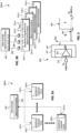
- FIGS. 1A and 1B illustrate example active phased array antennas 100-A and 100-B.
- Each of the active phased array antennas 100-A and 100-B includes a plurality of beamformer integrated circuits 102 and a plurality of antenna elements 104.
- a plurality of beamformer integrated circuits 102 of a given active phased array antenna 100 may be distributed along a first side 106 of a carrier board 108 and may be aligned uniformly with respect to corresponding positions of one or more antenna elements 104 positioned on a second side 110 of the carrier board 108, where the second side 110 is opposite the first side 106.
- a distance (also referred to as "spacing") between a given pair of antenna elements 104 disposed adjacent one another may be defined based on one or more operating parameters of the antenna elements, such as, for example, operating frequency and corresponding wavelength.
- the spacing requirements may apply to prevent or minimize occurrence of grating lobes and other undesirable distortions of the signals transmitted and/or received by the antenna elements 104.
- the first active phased array antenna 100-A may be configured to operate at a first frequency and the second active phased array antenna 100-B may be configured to operate at a second frequency, where the second frequency is greater than the first frequency.
- the first frequency may be 28 GHz and the second frequency may be 140 GHz.
- a first spacing S between antenna elements 104 of the first active phased array antenna 100-A configured to operate at the first (smaller) frequency is relatively large
- a second spacing s between the antenna elements 104 of the second active phased array antenna 100-B configured to operate at the second (larger) frequency is noticeably smaller than the first spacing S.
- FIG. 1C illustrates an example arrangement 100-C of the beamformer integrated circuit 102 with respect to a plurality of antenna elements 112, 114, 116, and 118.
- the beamformer integrated circuit 102 may be a radio frequency integrated circuit (RFIC) and may include a chip body 110 and a plurality of active channels 120 a, 120 b, 120 c , and 120 d , where each channel 120 a -120 d is electrically coupled to a different one of the antennas elements 112, 114, 116, and 118.
- RFIC radio frequency integrated circuit
- the beamformer integrated circuit 102 may include a digital control interface 122 via which the control signals arrive and leave the beamformer integrated circuit 102.
- the beamformer integrated circuit 102 may be configured to control operation of one or more antenna elements 112, 114, 116, and 118 using a corresponding one of the channels 120 a -120 d , based on the received signals or commands.
- the received signals or commands may be for example related to beamforming or beam steering operations that are to be performed. While a four-channel beamformer integrated circuit 102 is described in reference to FIGS. 1A-1C , the present disclosure is not limited thereto.
- a number of channels in a given beamformer integrated circuit 102 may be more or fewer than 4, such as, for example, 2, 12, 16, or any other number.
- a size of the beamformer integrated circuit 102 may decrease as the spacing between the antenna elements 112, 114, 116, and 118 in high-frequency phased arrays (e.g., active phased array antennas operating at frequencies greater than 100 GHz) becomes smaller. This phenomenon may be observed in corresponding sizes of the beamformer integrated circuits 102 of the active phased array antennas 100-A and 100-B described in reference to at least FIGS. 1A and 1B .
- an example active phased array antenna 200-A may include a main controller 202 communicatively coupled to a plurality of beamformer integrated circuits 102-1 to 102-n (such as beamformer integrated circuits 102 described in reference to FIGS. 1A-1C ) and configured to transmit and receive signals therefrom.
- the main controller which may also be understood as one or more processors, may be connected to the active phase array antenna, and thereby to the plurality of beamformer integrated circuits, instead of being included in it.
- the main processor When the main processor is communicatively coupled to, or connected to the plurality of beamformer integrated circuits, the main processor may be considered to have access to the plurality of beamformer integrated circuits and thus be able to control them for example by providing a signal, such as a control signal.
- the beamformer integrated circuits 102-1 to 102-n of the phased array 200-A may be digitally programmed, e.g., via an external controller, such as a modem or a computer, to recognize signals or commands from the main controller 202.
- a physical layout of the integrated circuits 102 on the carrier board 108 and/or pre-operational programming may include ensuring that each beamformer integrated circuit 102 is configured to be aware of (or to know) its own unique address, such that each beamformer integrated circuit 102 recognizes signals or commands directed by the main controller 202 to that particular beamformer integrated circuit 102.
- the main controller 202 includes a main controller digital control interface 204 that may be communicatively coupled to corresponding digital control interfaces 122-1 to 122-n of each of the beamformer integrated circuits 102-1 to 102-n.
- the beamformer integrated circuit 102 may be configured to use the digital control interface 122 to transmit signals to and receive signals from the main controller 202, where the transmitted and/or received signals may be related to controlling operation of the antenna elements 112, 114, 116, and 118 by the beamformer integrated circuit 102.
- FIG. 2B illustrates an example implementation 200-B of a communicative connection between the main controller 202 and a plurality of integrated circuits 102-1 to 102- n in accordance with the present disclosure.
- the digital control interface 204 of the main controller 202 and/or the digital control interface 112 of the beamformer integrated circuit 102 may be implemented as a serial peripheral interface (SPI).
- SPI serial peripheral interface
- the digital control interface 204 of the main controller 202 may interface with the digital control interface 112 of the beamformer integrated circuit 102 via a corresponding one of a "clock" pin 206, a "data write” pin 208, and a "data read” pin 210.
- the corresponding digital control interface 112 of each beamformer integrated circuit 102 may include one or more address pins 212-1 to 212- n .
- the one or more address pins 212-1 to 212- n of each beamformer integrated circuit 102 may be configured to be in a predefined electrical and/or electronic state, including, but not limited to, a state that is analog, digital, and/or logical in nature.
- the state of an address pin may correspond to an input voltage provided to the address pin.
- the predefined state of each address pin 212 may be set during manufacturing or printing of an active phased array antenna electrical circuit on the carrier board 108.
- the states of the one or more address pins 212-1 to 212- n of a given beamformer integrated circuit 102 may be indicative of a unique address associated with that beamformer integrated circuit 102.
- the unique address of the beamformer integrated circuit may be understood as an address that is used for identifying the beamformer integrated circuit from a plurality of other beamformer circuits that are comprised in the same system, for example, in the same active phased array antenna system.
- a given beamformer integrated circuit 102 uses, at least in some examples, the predefined state of its single address pin 212 (or the predefined states of a plurality of its address pins 212 considered collectively) to determine whether a signal being broadcasted by the main controller 202 is directed to that beamformer integrated circuit 102.
- the main controller 202 may be configured to include in a broadcasted data frame a unique address associated with a specific beamformer integrated circuit 102 that is the intended recipient of the broadcasted data frame.
- a number of address pins 212 necessary, for providing unique addresses, in each beamformer integrated circuit 102 of a given active phased array antenna may depend on a number of beamformer integrated circuits 102 that the main controller 202 controls.
- FIG. 3 illustrates an example two-level binary logic addressing approach 300 for the beamformer integrated circuit 102.
- the address pin 212 of the digital control interface 122 may be electrically coupled to a logic buffer 310.
- the address pin 212 may be set to be electrically pulled "low”, e.g., set to be electrically pulled to ground (GND), to correspond to a set state of the address pin 212 as being a low state 302.
- the address pin 212 of the digital control interface 122 may be set to be electrically pulled "high”, e.g., electrically pulled to a predefined voltage V DD , to correspond to a set state of the address pin 212 as being a high state 304.
- the buffer 310 may be configured to interpret the set pulled "low" state of the address pin 212 as corresponding to a logic zero (0) value and interpret the set pulled "high" state of that address pin 212 as corresponding to a logic one (1) value.
- the unique address of that beamformer integrated circuit 102 may be a digital value zero (0) and, where the set state of its single address pin 212 corresponds to a logic one (1) value, the unique address of that beamformer integrated circuit 102 may be a digital value one (1).
- the beamforming integrated circuit 102 including a first address pin 212-1 and a second address pin 212-2 may have a unique address "01", if the set state of the first address pin 212-1, e.g., according to the buffer 310, corresponds to a logic zero (0) value and the set state of the second address pin 212-2 corresponds to a logic one (1) value.
- the set state may be understood to correspond to an input voltage provided to an address pin.
- the different input voltages that may be provided to the address pin may be considered as set states that are available to the address pin. In case of logic zero and logic one for example, the address pin has thus two set states available for it.
- the beamforming integrated circuit 102 including a first address pin 212-1, a second address pin 212-2, and a third address pin 212-3 may have a unique address "110", if, e.g., according to the buffer 310, the set state of the first address pin 212-1 corresponds to a logic one (1) value, the set state of the second address pin 212-2 corresponds to a logic one (1) value, and the set state of the third address pin 212-3 correspond to a logic zero (0) value.
- the two-level binary logic approach provides using no fewer than six (6) address pins 212 on each beamformer integrated circuit 102 to generate 64 unique 6-bit addresses.
- the two-level binary logic approach 300 may require each beamformer integrated circuit 102 of a phased array having 1024 beamformer integrated circuits 102 to have at least 10 hard-wired address pins 212.
- a tighter spacing between the antenna elements and a demand for a smaller overall footprint of the active phased array antennas may cause less space to be available for pads of the beamformer integrated circuits 102.
- a number of beamformer integrated circuits 102 used in a given active phased array antenna may be increasing and, in some applications, may be in the thousands.
- An addressing methodology in accordance with the present disclosure that minimizes a number of address pins 212 necessary to communicate with a predefined number of beamformer integrated circuits using unique beamformer integrated circuit addresses may increase efficiency and dependability of large active phased array antennas. Thus, for one individual address pin, a larger address space than binary "0" and "1", may be available.
- a number of address pins required to address 256 beamformer integrated circuits 102 under the addressing methodology of the present disclosure may be four (4), or one-half the number of pins necessary to address the same number of beamformer integrated circuits 102 using a two-level binary addressing system.
- FIG. 4A illustrates an example addressing approach 400-A in accordance with the present disclosure.
- an electrical circuit 402 having one or more electric circuit components may be configured to detect a number M of set states of the address pins 212, where M is greater than two.
- the electrical circuit 402 may be configured to discern set states of the address pin 212 in addition to a high state and a low state detected using the two-level binary approach.
- the address pin 212 in this example has M set states that are available to it.
- the available voltage range between and including V GND , or 0 V, and V DD may be divided into M different levels, such as, for example, but not limited to, three (3) levels or four (4) levels.
- the electrical circuit 402 may be configured to discern corresponding set states of each of the address pin 212 as being one of either 3 or 4 possible set states.
- the electrical circuit 310 may be configured to detect a different set state of the address pin 212 when the input voltage V IN is between V GND and 0.5* V DD .
- the electrical circuit 310 may be configured to detect a different set state of the address pin 212 when the input voltage V IN is between 0.5* V DD and V DD .
- FIG. 4B illustrates an example implementation 400-B of the electrical circuit 402 configured to detect a number of M of unique set states, where M is greater than two.
- the electrical circuit 402 includes a plurality of logic buffers 404, 406, 408, such as non-Schmitt or Schmitt type buffers, electrically coupled to an address pin 212.
- each of logic buffers 404, 406, 408 may be configured to output a predefined logic state that may be same as or different from logic states of the other logic buffers 404, 406, 408.
- a voltage divider 410 coupled to the address pin 212 at the input to the buffers 404, 406, 408 may include a first resistor R 1 and a second resistor R 2 . As described in reference to FIGS. 5C and 6 , the voltage divider 410 may be configured to cause a voltage level of the address pin 212 to be a predefined voltage in response to the address pin 212 being left electrically open, i.e., being allowed to float. Thus, the logic buffers 404, 406, 408 receive the same input voltage as their inputs are connected to the same address pin 212.
- the buffers 404, 406, and 408 may generate output signals S0, S1 , and S2 , respectively.
- the output signals S0, S1 , and S2 may serve as input to an encoder logic unit 412 that, in turn, generates output signals A0 and A1.
- the output signals A0 and A1 then provide, at least partly, the unique address associated with the address pin 212.
- the encoder logic unit 412 may be configured to interpret logic values output by the buffers 404, 406, 408 as signals S0, S1 , and S2 and may generate output signals A0 and A1 responsive thereto.
- the additional address pin is coupled to logical buffers in the same manner as the address pin 212 is connected to the logic buffers 404, 406, 408.
- the logic buffers that receive their input from the additional address pin can also have a structure, which may be understood as hardware implementation, to those of the logic buffers 404, 406, 408. The same principle may apply also in case there are n additional address pins used for the unique address.
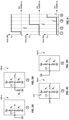
- FIGS. 5A, 5B, 5C, and 5D illustrate example circuits 500-A, 500-B, 500-C, and 500-D, each representative of a different one of a plurality of possible set states of the address pin 212 and a voltage level detected by the buffers 404, 406, and 408 during that set state.
- the first circuit 500-A illustrates a first set state of the address pin 212, e.g., the address pin 212 being set to be pulled low, e.g., to GND, such that the buffers 404, 406, and 408 detect a first input voltage level.
- the first input voltage level may be approximately 0 V.
- each of the buffers 404, 406, and 408 may be configured to output a logic state 0, as illustrated, for example, in FIG. 6 and Table 1.
- the second circuit 500-B illustrates a second set state of the address pin 212, e.g., the address pin 212 being set to be electrically coupled to a third resistor R 3 , such that the buffers 404, 406, and 408 detect a second input voltage level.
- the second input voltage level may be approximately 0.3* V DD .
- the first buffer 404 may be configured to output a logic state 1
- the second buffer 406 and the third buffer 408 may be configured to output a logic state 0 at outputs S0, S1, and S2 , respectively, as illustrated, for example, in FIG. 6 and Table 1.
- the third circuit 500-C illustrates a third set state of the address pin 212, e.g., the address pin 212 being set to be left open, such that the voltage divider 410 causes the buffers 404, 406, and 408 to detect a third input voltage level.
- the third input voltage level may be approximately 0.7* V DD .
- the first buffer 404 and the second buffer 406 may be configured to output a logic state 1 at outputs S0 and S1 , respectively, while the third buffer 408 may be configured to output a logic state 0 at output S2 , as illustrated, for example, in FIG. 6 and Table 1.
- the fourth circuit 500-D illustrates a fourth set state of the address pin 212, e.g., voltage V DD being applied to the address pin 212, such that the buffers 404, 406, and 408 detect a fourth input voltage level.
- the fourth input voltage level may be approximately V DD .
- each of the buffers 404, 406, and 408 may be configured to output a logic state 1 at outputs S0, S1, and S2 , respectively, as illustrated, for example, in FIG. 6 and Table 1.
- FIG. 7 illustrates an example circuit diagram 700 for implementing the addressing methodology in accordance with the present disclosure.
- the encoder logic unit 410 may be configured to detect the output signals S0, S1, S2 of the logic buffers 404, 406, 408, respectively, in thermometer code and may encode the detected thermometer code into two-bit binary code using encoder logic.
- the encoder 410 includes first and second logic AND gates 702-1, 702-2 and a logic XNOR gate 704.
- the logic AND gates 702-1, 702-2 and the logic XNOR gate 704 may be configured to generate the output logic states based on the output signals S0, S1 , and S2 of the buffers 404, 406, and 408.
- each of the logic AND gates 702-1, 702-2 may be configured to execute a logical conjunction operation, such that the logic AND gate outputs a high state (1) only if all inputs to that logic AND gate are high (1).
- the logic XNOR gate 704 may be configured to execute a logical connective operation, such that the logic XNOR gate 704 outputs a high state (1) if all inputs to the XNOR gate 704 are the same (i.e., all inputs are high (1) or all inputs are low (0)) and outputs a low state (0) if a state of at least one input to the XNOR gate 704 is different from that of the other inputs.
- a state of an output signal A1 of the encoder logic unit 410 may be based on a logic AND operation performed on the output signals S0 and S1 by the logic AND gate 702-1.
- a state of the output signal A0 of the encoder logic unit 410 may be based on a logic AND operation performed, by the logic AND gate 702-2, on the output signal S0 and a result of a logic XNOR operation performed on the output signals S2 and S1 by the logic XNOR gate 704.
- the example implementations described above may have several benefits.
- the hard-wired addressing approach of the present disclosure is platform-independent and may be implemented in any digital control interface configured to provide control signals to the integrated circuits.
- a single pin may be configured to address three beamformer integrated circuits without using any additional external components.
- the number of integrated circuits that may be addressed using a predefined number of hard-wired address pins may be doubled.
- M the number of addressable beamformer integrated circuits for x address pins
- M may also be greater than four with additional logic buffers configured to change states in response to detecting additional predefined threshold voltage levels.
- the examples introduced above may also have the benefit of allowing efficient design of very large active phased array antenna systems, such as active phased array antennas operating at frequencies >100 GHz, that include a large number of very small beamformer integrated circuits that have limited available pad space. Further, adding buffer circuits and encoder logic may be executed without occupying additional area in silicon. Moreover, the example embodiment described above may be compatible with control interfaces using two-level binary logic.
- circuitry refers to all of the following: (a) hardware-only circuit implementations, such as implementations in only analog and/or digital circuitry, and (b) combinations of circuits and software (and/or firmware), such as (as applicable): (i) a combination of processor(s) or (ii) portions of processor(s)/software including digital signal processor(s), software, and memory(ies) that work together to cause an apparatus to perform various functions, and (c) circuits, such as a microprocessor(s) or a portion of a microprocessor(s), that require software or firmware for operation, even if the software or firmware is not physically present.
- This definition of 'circuitry' applies to all uses of this term in this application.
- the term 'circuitry' would also cover an implementation of merely a processor (or multiple processors) or a portion of a processor and its (or their) accompanying software and/or firmware.
- the term 'circuitry' would also cover, for example and if applicable to the particular element, a baseband integrated circuit or applications processor integrated circuit for a mobile phone or a similar integrated circuit in a server, a cellular network device, or another network device.
- the above-described embodiments of the circuitry may also be considered as embodiments that provide means for carrying out the embodiments of the methods or processes described in this document.
- the techniques and methods described herein may be implemented by various means. For example, these techniques may be implemented in hardware (one or more devices), firmware (one or more devices), software (one or more modules), or combinations thereof.
- the apparatus(es) of embodiments may be implemented within one or more application-specific integrated circuits (ASICs), digital signal processors (DSPs), digital signal processing devices (DSPDs), programmable logic devices (PLDs), field programmable gate arrays (FPGAs), graphics processing units (GPUs), processors, controllers, microcontrollers, microprocessors, other electronic units designed to perform the functions described herein, or a combination thereof.
- ASICs application-specific integrated circuits
- DSPs digital signal processors
- DSPDs digital signal processing devices
- PLDs programmable logic devices
- FPGAs field programmable gate arrays
- GPUs graphics processing units
- processors controllers, microcontrollers, microprocessors, other electronic units designed to perform the functions described herein, or a combination thereof.
- the software codes may be stored in a memory unit and executed by processors.
- the memory unit may be implemented within the processor or externally to the processor. In the latter case, it can be communicatively coupled to the processor via any suitable means.
- the components of the systems described herein may be rearranged and/or complemented by additional components in order to facilitate the achievements of the various aspects, etc., described with regard thereto, and they are not limited to the precise configurations set forth in the given figures, as will be appreciated by one skilled in the art.
- Embodiments described herein may be implemented in a communication system, such as in at least one of the following: Global System for Mobile Communications (GSM) or any other second generation cellular communication system, Universal Mobile Telecommunication System (UMTS, 3G) based on basic wideband-code division multiple access (W-CDMA), high-speed packet access (HSPA), Long Term Evolution (LTE), LTE-Advanced, a system based on IEEE 802.11 specifications, a system based on IEEE 802.15 specifications, and/or a fifth generation (5G), as well as 5G-Advanced (i.e. 3GPP NR Rel-18 and beyond), mobile or cellular communication system.
- GSM Global System for Mobile Communications
- UMTS Universal Mobile Telecommunication System
- 3G Universal Mobile Telecommunication System
- W-CDMA basic wideband-code division multiple access
- HSPA high-speed packet access
- LTE Long Term Evolution
- LTE-Advanced Long Term Evolution
- 5G fifth generation
- the embodiments described herein may be implemented in
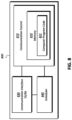
- the apparatus 800 of FIG. 8 illustrates an example embodiment of an apparatus that may be an access node or be comprised in an access node and which may be used to provide a signal to a beamformer integrated circuit for performing beamforming or beam steering.
- the beamformer integrated circuit may also be comprised in the access node and may be addressed according to any of the examples described above.
- the apparatus may be, for example, a circuitry or a chipset applicable to an access node to realize the described embodiments.
- the apparatus 800 may be an electronic device comprising one or more electronic circuitries.
- the apparatus 800 may comprise a communication control circuitry 800 such as at least one processor, and at least one memory 820 including a computer program code (software) 822 wherein the at least one memory and the computer program code (software) 822 are configured, with the at least one processor, to cause the apparatus 800 to carry out any one of the example embodiments of the access node described above.
- a communication control circuitry 800 such as at least one processor, and at least one memory 820 including a computer program code (software) 822 wherein the at least one memory and the computer program code (software) 822 are configured, with the at least one processor, to cause the apparatus 800 to carry out any one of the example embodiments of the access node described above.
- the memory 820 may be implemented using any suitable data storage technology, such as semiconductor-based memory devices, flash memory, magnetic memory devices and systems, optical memory devices and systems, fixed memory and removable memory.
- the memory may comprise a configuration database for storing configuration data.
- the configuration database may store current neighbour cell list, and, in some example embodiments, structures of the frames used in the detected neighbour cells.
- the memory 820 may store unique addresses of a plurality of beamformer integrated circuits.
- the apparatus 800 may further comprise a communication interface 830 comprising hardware and/or software for realizing communication connectivity according to one or more communication protocols.
- the communication interface 830 may provide the apparatus with radio communication capabilities to communicate in the cellular communication system.
- the communication interface may, for example, provide a radio interface to terminal devices.
- the apparatus 800 may further comprise another interface towards a core network such as the network coordinator apparatus and/or to the access nodes of the cellular communication system.
- the apparatus 800 may further comprise a scheduler 840 that is configured to allocate resources.
Landscapes
- Engineering & Computer Science (AREA)
- Computer Hardware Design (AREA)
- Physics & Mathematics (AREA)
- Mathematical Physics (AREA)
- Computer Networks & Wireless Communication (AREA)
- Computing Systems (AREA)
- General Engineering & Computer Science (AREA)
- Signal Processing (AREA)
- Power Engineering (AREA)
- Semiconductor Integrated Circuits (AREA)
- Read Only Memory (AREA)
Applications Claiming Priority (1)
| Application Number | Priority Date | Filing Date | Title |
|---|---|---|---|
| FI20226058 | 2022-11-29 |
Publications (2)
| Publication Number | Publication Date |
|---|---|
| EP4380071A2 true EP4380071A2 (de) | 2024-06-05 |
| EP4380071A3 EP4380071A3 (de) | 2024-07-31 |
Family
ID=88833521
Family Applications (1)
| Application Number | Title | Priority Date | Filing Date |
|---|---|---|---|
| EP23209640.4A Pending EP4380071A3 (de) | 2022-11-29 | 2023-11-14 | Adressierung für integrierte schaltungen |
Country Status (3)
| Country | Link |
|---|---|
| US (1) | US20240178841A1 (de) |
| EP (1) | EP4380071A3 (de) |
| CN (1) | CN118118009A (de) |
Families Citing this family (1)
| Publication number | Priority date | Publication date | Assignee | Title |
|---|---|---|---|---|
| US20250275231A1 (en) * | 2024-02-23 | 2025-08-28 | Renesas Electronics America Inc. | Series addressing scheme for smart power stages of high current applications |
Family Cites Families (5)
| Publication number | Priority date | Publication date | Assignee | Title |
|---|---|---|---|---|
| US7827330B2 (en) * | 2007-07-27 | 2010-11-02 | Microchip Technology Incorporated | Configuring multi-bit slave addressing on a serial bus using a single external connection |
| US8643168B1 (en) * | 2012-10-16 | 2014-02-04 | Lattice Semiconductor Corporation | Integrated circuit package with input capacitance compensation |
| US10686258B2 (en) * | 2017-09-18 | 2020-06-16 | Integrated Device Technology, Inc. | Hard-wired address for phased array antenna panels |
| US10804616B2 (en) * | 2018-03-27 | 2020-10-13 | Viasat, Inc. | Circuit architecture for distributed multiplexed control and element signals for phased array antenna |
| US12119533B2 (en) * | 2021-12-15 | 2024-10-15 | Npx B.V. | Beamformer integrated circuits with multiple-stage hybrid splitter/combiner circuits |
-
2023
- 2023-11-13 US US18/507,524 patent/US20240178841A1/en active Pending
- 2023-11-14 EP EP23209640.4A patent/EP4380071A3/de active Pending
- 2023-11-27 CN CN202311589952.7A patent/CN118118009A/zh active Pending
Also Published As
| Publication number | Publication date |
|---|---|
| CN118118009A (zh) | 2024-05-31 |
| EP4380071A3 (de) | 2024-07-31 |
| US20240178841A1 (en) | 2024-05-30 |
Similar Documents
| Publication | Publication Date | Title |
|---|---|---|
| EP4380071A2 (de) | Adressierung für integrierte schaltungen | |
| US20190327669A1 (en) | Paging method and device | |
| CN115136665A (zh) | 传送集成接入和回传信息的方法及系统 | |
| US20130235755A1 (en) | Method and apparatus for performing measurements in a multi carrier environment | |
| CN110192349B (zh) | 用于基于向量的ldpc基础矩阵的使用和生成的方法和装置 | |
| CN115428505B (zh) | 激活和去激活周期性参考信号 | |
| CN109644071B (zh) | 用于urllc中的通信的方法和装置 | |
| ES2880381T3 (es) | Equilibrio de carga en redes celulares | |
| IL266225B2 (en) | Beam measurement method and apparatus | |
| ES3062426T3 (en) | Resource configuration method and device | |
| KR20210040531A (ko) | 와이어를 이용한 반도체 장치 및 스택형 반도체 패키지 | |
| EP4106243A1 (de) | Informationsübertragungsverfahren, -vorrichtung und -einrichtung | |
| CN114788328A (zh) | 一种传输控制信息的方法 | |
| CN112291821A (zh) | 信息配置方法、装置、相关设备及存储介质 | |
| EP3624526B1 (de) | Ressourcenanzeigeverfahren und -vorrichtung sowie computerspeichermedium | |
| US20200344575A1 (en) | Indication method for system broadcast information, network device, and terminal device | |
| CN117272916B (zh) | 一种版图自动生成方法、装置、设备和可读存储介质 | |
| US20240340148A1 (en) | Beam indication method and apparatus, terminal and base station | |
| CN116486855A (zh) | 改进的掩模rom装置 | |
| CN116980989A (zh) | 信息上报方法、装置、终端、基站及存储介质 | |
| EP3520554B1 (de) | Funkressourcenverwaltungsanforderungen für verbesserte maschinenartige kommunikation auf basis der überwachung eines physikalischen downlink-steuerkanals einer maschinenartigen kommunikation | |
| CN113498206B (zh) | 信息传输方法及装置 | |
| US20130222019A1 (en) | Semiconductor integrated circuit, semiconductor device, and method of designing semiconductor integrated circuit | |
| JP7382441B2 (ja) | スイッチング回路、直流電力出力装置、無線電力伝送システム、太陽光発電システム、出力制御方法及びプログラム | |
| CN110972146B (zh) | 无线网络的配置方法及网络设备 |
Legal Events
| Date | Code | Title | Description |
|---|---|---|---|
| PUAI | Public reference made under article 153(3) epc to a published international application that has entered the european phase |
Free format text: ORIGINAL CODE: 0009012 |
|
| STAA | Information on the status of an ep patent application or granted ep patent |
Free format text: STATUS: THE APPLICATION HAS BEEN PUBLISHED |
|
| AK | Designated contracting states |
Kind code of ref document: A2 Designated state(s): AL AT BE BG CH CY CZ DE DK EE ES FI FR GB GR HR HU IE IS IT LI LT LU LV MC ME MK MT NL NO PL PT RO RS SE SI SK SM TR |
|
| PUAL | Search report despatched |
Free format text: ORIGINAL CODE: 0009013 |
|
| AK | Designated contracting states |
Kind code of ref document: A3 Designated state(s): AL AT BE BG CH CY CZ DE DK EE ES FI FR GB GR HR HU IE IS IT LI LT LU LV MC ME MK MT NL NO PL PT RO RS SE SI SK SM TR |
|
| RIC1 | Information provided on ipc code assigned before grant |
Ipc: H04W 16/28 20090101ALI20240625BHEP Ipc: H01Q 3/34 20060101ALI20240625BHEP Ipc: H04B 7/06 20060101AFI20240625BHEP |
|
| STAA | Information on the status of an ep patent application or granted ep patent |
Free format text: STATUS: REQUEST FOR EXAMINATION WAS MADE |
|
| 17P | Request for examination filed |
Effective date: 20250131 |